A Novel Method for Embedding Semiconductor Dies within Textile Yarn to Create Electronic Textiles


Advanced Textiles Research Group, Nottingham Trent University, Nottingham NG1 4FQ, UK
*
Authors to whom correspondence should be addressed.
Fibers 2019, 7(2), 12; https://0-doi-org.brum.beds.ac.uk/10.3390/fib7020012
Submission received: 21 December 2018
/
Revised: 18 January 2019
/
Accepted: 21 January 2019
/
Published: 26 January 2019
(This article belongs to the Special Issue Electronically Active Textiles)
Abstract
:Electronic yarns (E-yarns) contain electronics fully incorporated into the yarn’s structure prior to textile or garment production. They consist of a conductive core made from a flexible, multi-strand copper wire onto which semiconductor dies or MEMS (microelectromechanical systems) are soldered. The device and solder joints are then encapsulated within a resin micro-pod, which is subsequently surrounded by a textile sheath, which also covers the copper wires. The encapsulation of semiconductor dies or MEMS devices within the resin polymer micro-pod is a critical component of the fabrication process, as the micro-pod protects the dies from mechanical and chemical stresses, and hermetically seals the device, which makes the E-yarn washable. The process of manufacturing E-yarns requires automation to increase production speeds and to ensure consistency of the micro-pod structure. The design and development of a semi-automated encapsulation unit used to fabricate the micro-pods is presented here. The micro-pods were made from a ultra-violet (UV) curable polymer resin. This work details the choice of machinery and methods to create a semi-automated encapsulation system in which incoming dies were detected then covered in resin micro-pods. The system detected incoming 0402 metric package dies with an accuracy of 87 to 98%.
1. Introduction
Clothing consists of textile fibers, which are either woven or knitted to produce fabric for both protective and aesthetic purposes. Interactive textiles add a third dimension to traditional textiles [1], with the inclusion of interactivity often achieved using electronics [2]. Interest in the integration of electronics into textiles has increased significantly in recent years, leading to a number of innovative textiles with integrated lighting [3], computing [4], and sensing capabilities [5] for a variety of applications. Electronic textiles can also be used to generate and store electricity [6]. A recent review of the history of electronic textiles is available elsewhere [7], which gives details of a wide variety of electronic textile products that have been designed and developed.
Electronics can be integrated into textiles in one of three ways that can be described as generations of electronic textiles. In the first generation of electronic textiles, electronic components were mounted directly onto the surface of garments. The electronics did not form a part of the structure of the textiles. Examples include sports bras with heart-rate monitors that are attached to the garment with snap fasteners [8]. Thin layers with electronic functionality can be printed directly onto the surface of flexible substrates that include textiles [9]. Deposition processes can also be used to add electronic functionality to the surface of textiles, for example, in the production of flexible photovoltaics [10]. The second generation involved integrating electronics into the structure of garments through knitting, weaving, and embroidery to add electronic functionality. Most focused on the use of conductive fibers to create electrodes or conductive pathways, such as pressure sensor fabrics [11], fabric transducers [12], and a Wearable Motherboard™ [13].
The third generation of electronic textiles could be described as yarns into which sensors and other electronic components were incorporated. E-textile development projects in which electronic functionality has been incorporated at a yarn level include:
- A recent innovation by MIT in which LEDs (light-emitting diodes) and photodiodes were incorporated into a fiber as part of an extrusion process [14]. The polymer extrusion process is likely to result in a yarn with poor tensile strength [15] due to the inability to draw the filaments soon after extrusion without damaging the copper wire interconnects. This will influence the processability of the yarns using standard textile fabrication processes, such as knitting. The MIT concept is also limited to two-terminal devices, which will restrict the range of devices and the scope of functionality that can be incorporated into these yarns;
- The European Union funded PASTA project in which E-Thread® was developed. This saw a die connected to two conducting interconnects, and the die and interconnects covered in a fibrous cover [16]. These dies were not protected by encapsulation, and the E-Thread® could not be subjected to washing processes.The E-Thread® could only be constructed using two-terminal devices, limiting the range of devices, and therefore functions, that can be incorporated. E-thread containing RFID (radio frequency identification) devices are produced by Primo1D [17];
- the Wearable Computing Lab at ETH Zurich have integrated polymer strips, populated with surface mounted devices (SMD) and conductive tracks, during the weaving process [18]. The polymer strips were used as ‘yarns’, but their insertion restricts the shear behavior of the final textile fabric; and the use of a standard bare die (not encapsulated) limits the degree of bending that the strips can withstand. The electronics were exposed on the surface of the textile and rapidly failed after washing.
The maintenance of ‘fiber-based’ characteristics within an electronic textile is desirable [19]. Electronic yarn, (E-yarn) [20] was a further progression from the second generation of E-textiles that fulfilled this aim. Previously, conductive components and electronics replaced much or all of the textile fibers within textile structures, altering the properties of the completed textile. The difference between this third generation product and previous generations of electronic textiles was that the electronics were included within textile yarns that retained their textile properties, unlike, say, fiber optics included within electronic textiles. Electronics were contained within small micro-pods within E-yarn, leaving more than 90% of the volume of the E-yarn as textile fibers. The textile properties of E-yarn meant that it could be processed in knitting and weaving machines. The advantage of creating a textile-based E-yarn was that yarn properties could be retained to a greater extent than when using other materials. In particular:
- The mechanical properties of the textile yarn were not adversely affected by the inclusion of electronics.
- Moisture wicking and moisture retention occurred as in a normal textile yarn.
- The E-yarn could be colored using textile dyeing methodology.
This allowed for electronics to be integrated in a highly discrete way, with electronic yarns being undetectable to the end user. Several types of E-yarn have been incorporated into a variety of textiles, as reported elsewhere in the literature.
E-yarn Structure and Manufacturing Process
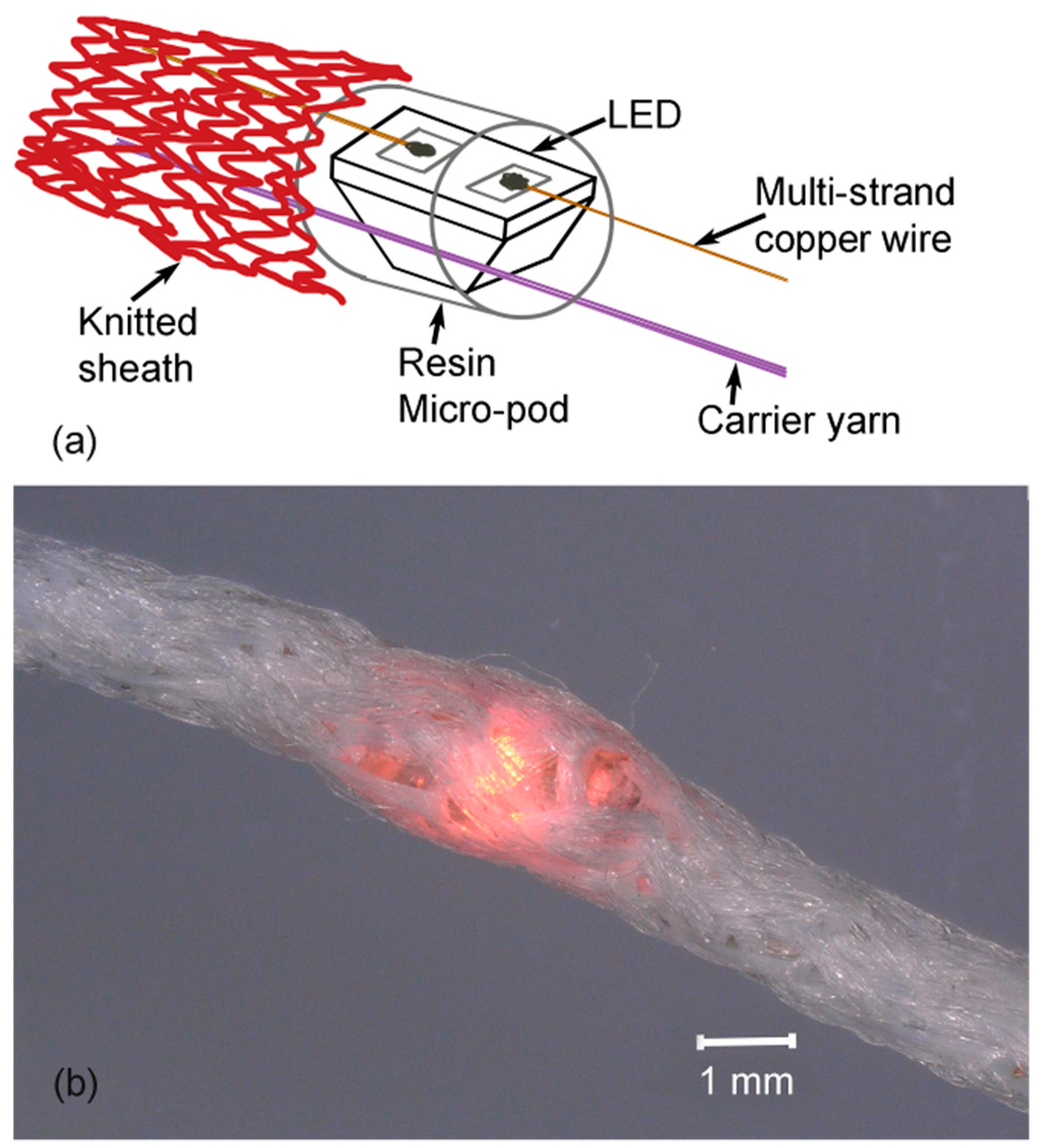
Figure 1a shows a schematic of the E-yarn structure, with a photo of an E-yarn containing an LED in Figure 1b.
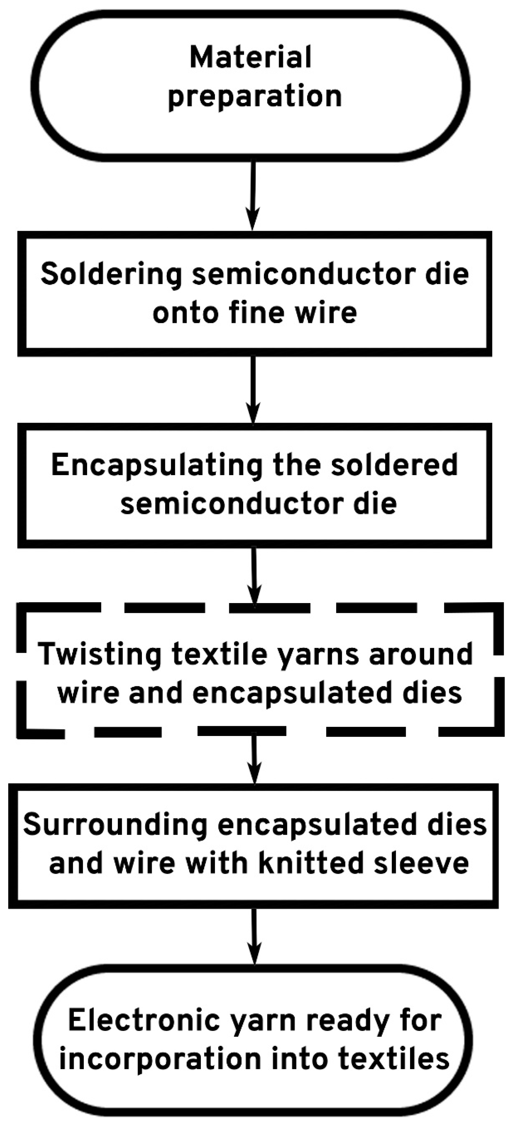
The production of E-yarn consisted of four main steps [21]: Firstly, a package die was soldered onto a fine copper wire. Encapsulation of the die and solder joints followed. The final two stages involved the addition of textile yarns twisted around the copper wire and attached micro-pods, before insertion of the construction into a soft, fibrous sleeve using a small-diameter circular warp knitting machine (RIUS; Barcelona, Spain). This gave the resulting E-yarn a textile feel, so that it could then be used in knitting and weaving machinery for garment production. The flow chart in Figure 2 shows the main steps in the process. The twisting of textile yarns around the core was not required for all E-yarn constructions, so it is shown within a box surrounded by dashed lines in Figure 2.
This work concentrates on the production of E-yarns. The E-yarns included within some of the prototypes in the literature were fabricated using a laborious hand-crafting process; this is both time consuming and may induce issues of repeatability into the production process. By automating the production process, a larger quantity of yarns can be produced, which will be required for industrial adoption. This has been ongoing work over many years, and as a result, an overview of the automation process is available elsewhere in the literature [21], as well as details of some prototypes produced with early versions of the automated process [22].
This paper will specifically concentrate on the automation of the encapsulation process. Here, encapsulation refers to the process of applying a fluid sealing compound into a small and pre-defined area around a die to produce a micro-pod. This encapsulated the die and the solder joints that attached it to copper wire. The sealing compound protected the electrical component from environmental effects, such as humidity and dust, and meant that the resulting E-yarn could be washed. Other benefits included improved electrical insulation, reliability, and protection against damage. The encapsulation was required to cover dies and solder joints only, leaving the wire interconnections between dies free to flex within the E-yarn. The resulting E-yarn consisted of more than 95% fibers, as the encapsulation volume was minimal.
The micro-pod was also used to create a bond between the copper wire and a carrier yarn that carried the mechanical stress in the E-yarn. The carrier yarn was placed alongside the copper wire, so that it became included within the micro-pod during the encapsulation process. The purpose of the encapsulation was to enhance the robustness and reliability of the E-yarn in the final product.
The aim of the work was to automate the stage in the E-yarn production process in which the package dies soldered to copper wire were covered in resin micro-pods. The resulting process allowed for repeated, automated production of micro-pods, increasing the E-yarn production speed from the previous manual process and paving the way for continuous, reliable, and repetitive production of E-yarn. This paper outlines key design considerations.
Ultimately, an automated process was created to form micro-pods around package dies that had been previously soldered to copper wire. The dies were encapsulated within a cylindrical mold, then removed using this automated process. A carrier yarn included within the encapsulation was shown to increase the tensile strength of the construction, enabling removal of the micro-pod from the mold. FTIR (Fourier Transform Infrared) analysis was used to assess optimal curing times for the resin micro-pods.
2. Design Considerations and Methodology
A methodology was developed to automate the encapsulation of semiconductor dies soldered onto multi-strand copper wire. This required an approach in which materials and machinery were selected, in conjunction with decisions about optimal processes to form the encapsulation micro-pods, and the order of operations. The challenge was to demonstrate that E-yarn production could be automated, so that the manufacturing process could ultimately be scaled up and commercialized. The selection of machinery and methods was based on the availability within the time and budgetary constraints of this project.
The core materials of E-yarn were copper wire and semiconductor dies. A 7-strand copper wire with a 50 µm strand diameter (Knight Wire, Potters Bar, UK) was chosen due to its flexibility compared with a single-strand wire of the same diameter. Semiconductor package dies of size 0402 were used. The examples shown in this work are a Kingbright KPHHS-1005SURCK Red LED, 630 nm 1005 (0402), Rectangle Lens package (RS Components, Corby, UK), and a thermistor (Murata 10 kΩ 100 Mw 0402 SMD NTC thermistor; part number NCP15XH103F03RC; Murata, Kyoto, Japan). This wire and these semi-conductor devices were based on those previously chosen in another work [21].
2.1. Resin Selection
The selection of the encapsulation material involved consideration of:
- Ability to dispense small amounts of encapsulant around the package dies;
- A method of curing that could be carried out without damage to the package dies;
- The speed of the curing process;
- Fabrication of a micro-pod that could withstand washing;
- Creation of a micro-pod that could transmit light from a package LED;
- Flexibility, for compatibility with surrounding textile materials.
The choice of the curing method for the encapsulation material was considered first. Encapsulating dies using a heat-curing method was undesirable due to the negative effect of the heating process on the die itself, and the time taken for many heat-curable resins to cure fully. Heat curing could also have led to mechanical failure of electronic components due to temperature-induced elastic or plastic deformation [23]. For these reasons, a photo-initiated curing method was preferred. Additional advantages included a low operational cost, easy maintenance, and the small footprint of space required for machinery. Moreover, an ultra-violet (UV)-curable coating reduced solvent emission, since most of the formulation was composed of oligomers and reactive diluents [24].
- A resin, such as an oligomer or prepolymer, which is an unsaturated double bond or cyclic structure capable of ring opening;
- Reactive diluents (monomers with varying degrees of unsaturation), which have two functions: one is to reduce the viscosity of the systems, while the other function of the diluents is render crosslinking;
- A photo initiator, which absorbs UV radiation and generates reactive species that can initiate the polymerization.
Commercially-available UV-curable resins can be categorized by the polymerization mechanisms through which curing takes place. One uses radical polymerisation of monomers, such as acrylates or unsaturated polyesters. The other main method uses cationic polymerisation of multifunctional groups, such as epoxides and vinyl ethers [26]. An acrylated urethane was chosen for this research: Dymax 9001-E-V3.5 (Dymax, Torrington, UK). This is transparent to visible light, making it suitable for encapsulation of LEDs. Moreover, this resin is flexible, so it is suitable for textile applications. The resin is also used in bonding applications in the electronics industry, meaning that it has been fully tested on a range of electronic devices [27].
2.2. Curing the Resin
The chosen Dymax 9001 resin was designed to be cured with light at wavelengths from 320–450 nm [27]. Curing was carried out in the center of this range, with a 385 nm UV (BlueWave® QX4® LED Multi-Head Spot-Curing System; Intertronics, Kidlington, UK). The time required to cure the resin fully was assessed initially by checking that liquid resin became solid after the curing process. An investigation of the optimal curing time was carried out using Fourier Transform Infrared Spectroscopy (FTIR). For these experiments, 3 µL of resin (typical for a 1 mm diameter cylindrical encapsulation) was dispensed onto a plate of PTFE (polytetrafluoroethylene). Samples were cured for 10 s, 20 s, 30 s, and 50 s by exposure to the 385 nm UV light source. The samples were then kept in black bags to avoid any curing by visible light, before their transmission spectra were analyzed in an FTIR spectrometer (Perkin Elmer Spectrum Two; Llantrisant, UK).
2.3. Encapsulation Mold Design
Resin micro-pods can be formed by applying a small amount of resin around a die or by placing the die (soldered to copper wire) within a mold, then injecting resin into the mold. The latter method was chosen to ensure uniformity of the micro-pod size. The design of this encapsulation mold was a crucial part of the process, with careful consideration paid to the shape, size, and orientation. A cylindrical micro-pod shape was chosen for encapsulating the soldered semiconductor, as this shape had minimal edges. This shape was also easier to pass through the small-diameter warp-knitting machine that was used in a later stage of production of E-yarn, when the micro-pods were surrounded by a knitted sleeve. Cylindrical micro-pods were also more likely to be comfortable to the end users as the circular cross-section of the encapsulation was compatible with the cross-section of traditional textile yarn. The diameter of the encapsulation had to be minimized to keep the overall diameter of the yarn as thin as possible, thus suitable for embedding within ordinary garments: A thicker encapsulation would lead to a thicker final yarn. Conversely, the diameter of the mold had to allow the resin to flow in a way that would fully cover and protect the electronic component.
2.3.1. Mold Material
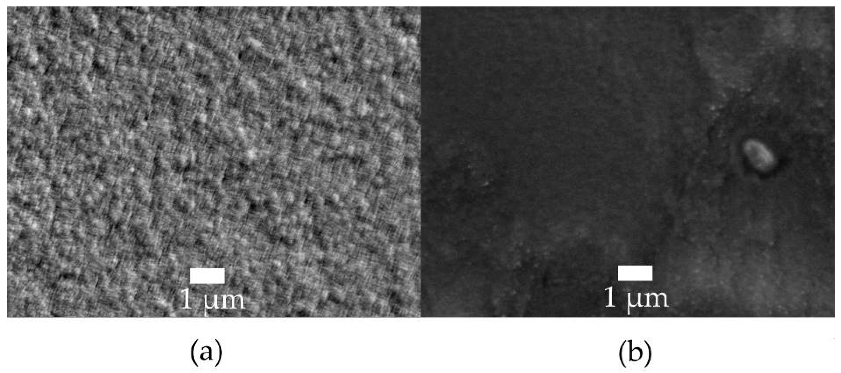
The selected cylindrical micro-pod shape could be formed within a tubular mold. A mold material was required that minimized adhesion of the cured resin to the mold wall to minimize the force required to release the micro-pod from the mold. The wetting properties of the inner mold surfaces were important for the resin dispensing process. The mold walls were also required to be UV-transparent to permit curing of the resin. Two potential mold materials were examined that fulfilled these criteria, and were available in tube form (which was the preferred shape for the mold; discussed in 2.3.2, below): Silicone (2mm Silicone Tube, part number a16090800ux0404; Sourcingmap, Mountain View, CL, USA) and PTFE (RS PRO Long Coil Tubing Without Connector, Fluoropolymer 22 bar, −40 → +150 °C; RS Pro, Corby, Northants, UK). The internal surface structures of both materials were assessed using a scanning electron microscope (Scanning Electron Microscope, JEOL JSM-840A, SEMTech Solutions, Billerica, MA, USA)
2.3.2. Mounting of the Mold
The flexible tube that was chosen for the mold required mounting within a stable structure through which UV light could penetrate. The tube was placed within the body of a polypropylene syringe (Metcal PP Adhesive Dispenser Syringe; Techcon Systems, Garden Grove, CL, USA), with the back of the syringe removed to facilitate later mounting within an automated encapsulation system. The tube was held in place within the syringe using Transil 40-1 silicone elastomer (Mouldlife, Suffolk, UK). Transil 40-1 is a two-component silicone elastomer that crosslinks at room temperature by a poly-addition reaction to form a transparent, elastic material. The transparency was an advantage, minimizing UV blocking during the curing process, which was critical for this application. Transil 40-1 A and Transil 40-1 B were mixed by weight in a fixed ratio of 1:10 of parts A and B, respectively. The mixture was then degassed for 10 min and poured slowly into the outer part of a plastic syringe, with the flexible tube held inside the syringe. Figure 5 shows the silicone mold around the flexible tube in which encapsulation was carried out. The whole syringe, with the silicone and the flexible tube inside it, were mounted vertically within a bracket. Vertical mounting ensured that the resin flowed evenly over the die, rather than falling to one side. An image of the mold mounted to the encapsulation system is shown later in this work (Section 3).
2.4. Resin Dispensing
There was a need to inject a small, pre-determined volume of resin into the mold to surround each package die held within it. A preeflow® eco-PEN Precision Volumetric Dosing Pump (Intertronics, Kidlington, Oxfordshire, UK) was used to apply resin and create a micro-pod around the electronic components. This system used volumetric, positive-displacement dosing, which gave both accuracy and repeatability. This dosing system could dispense small quantities, with a minimum volume of 0.001 mL, with flow speeds of 0.12–1.48 mL/min.
2.5. Carrier Yarn
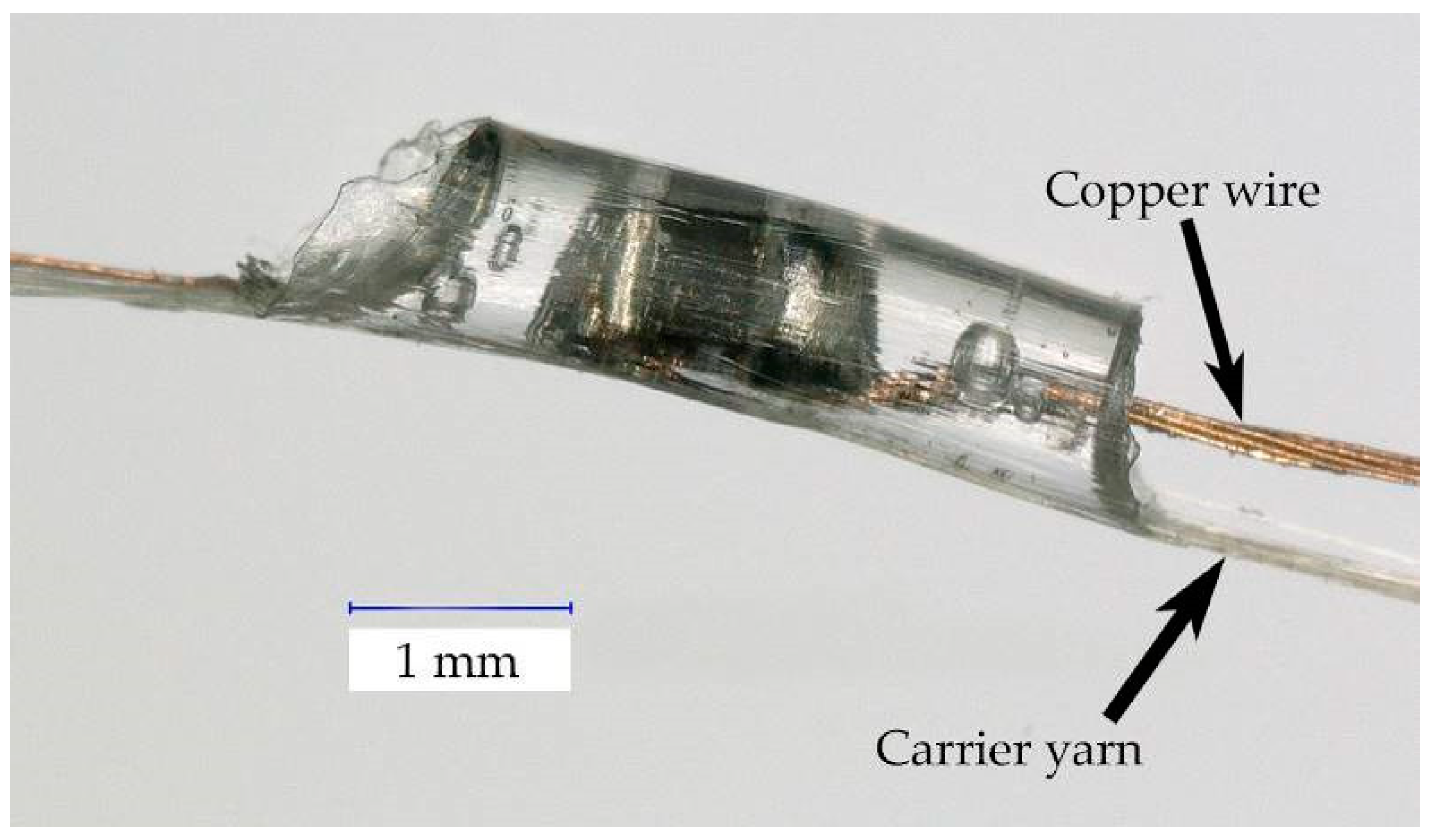
To enhance the mechanical properties of the completed E-yarn, the soldered semiconductor die was encapsulated along with a carrier yarn. The role of the carrier yarn was to support the soldered joint, protecting it and the copper wire from mechanical stresses during demolding and during subsequent E-yarn formation processes. 100 Dernier Vectran™ (Kururay, Tokyo, Japan) was chosen for its high tensile strength [21] combined with its flexibility. Figure 3 shows a soldered semiconductor die (a thermistor) and Vectran™ carrier yarn running alongside the copper wire; both included within a resin micro-pod that forms the encapsulation.
2.6. Tensile Force Required to Remove the Micro-pod from the Mold
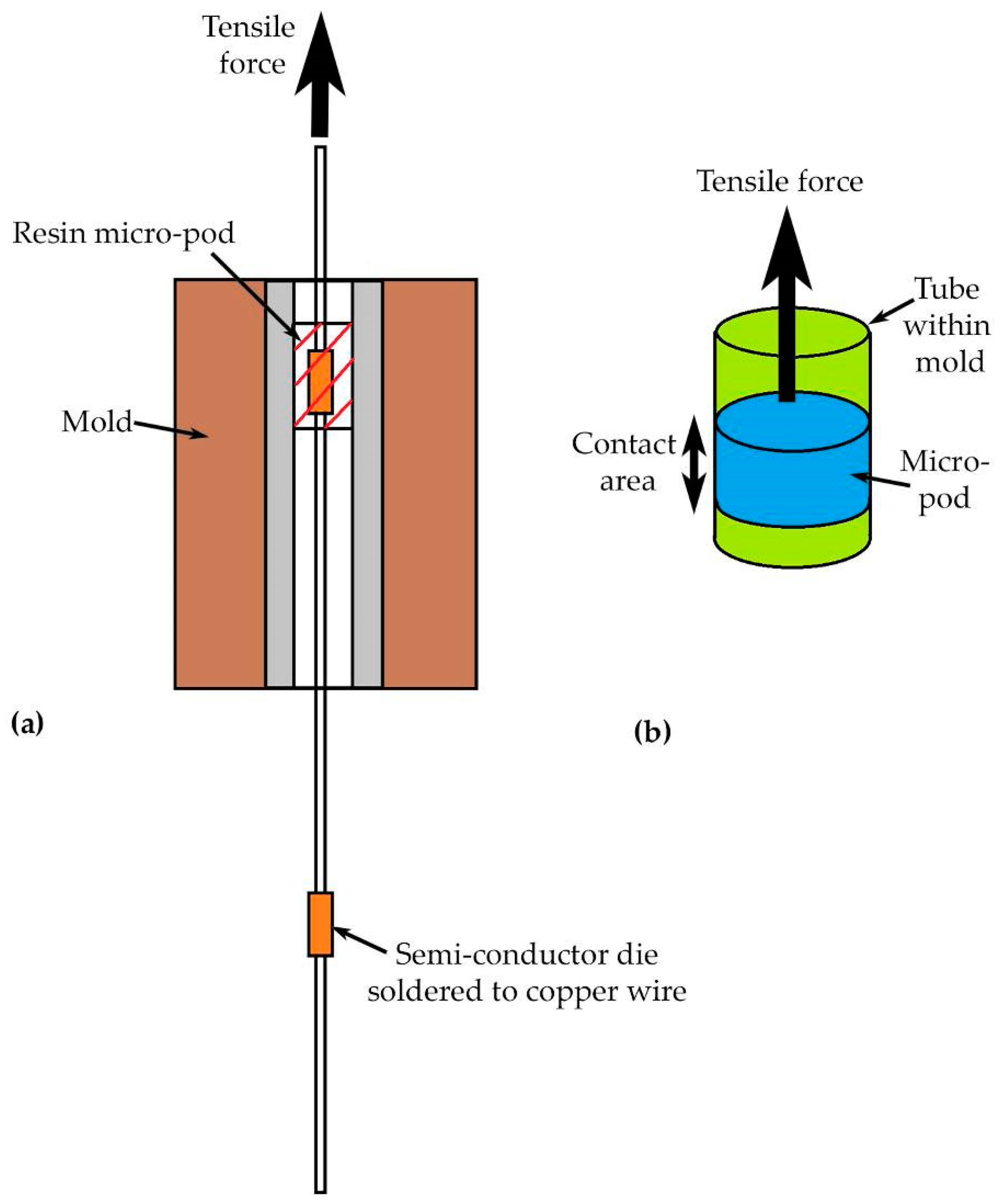
Pulling on the carrier yarn provided a method of removing encapsulated dies from the mold in which the micro-pod was formed. Experiments were carried out to find the tensile forces required to remove cured micro-pods from the mold. The results were compared with the tensile forces required to break the carrier yarn. This established the limitations of the molding system; indicating at which micro-pod length friction forces would prevent removal from the mold using the carrier yarn to provide the demolding force. To find the tensile force required to demold the micro-pod, the mold was mounted in a zwickiLine tensile tester (Z2.5; Zwick/Roell, Ulm, Germany). Micro-pods were pulled from a mold as shown in Figure 4a. Measurements were taken of the tensile force required to remove encapsulated dies from the mold. This force was expected to increase in proportion to the amount of contact surface between the cured resin and the mold tube walls. Figure 4b shows this contact area.
2.7. Automating the Production Process
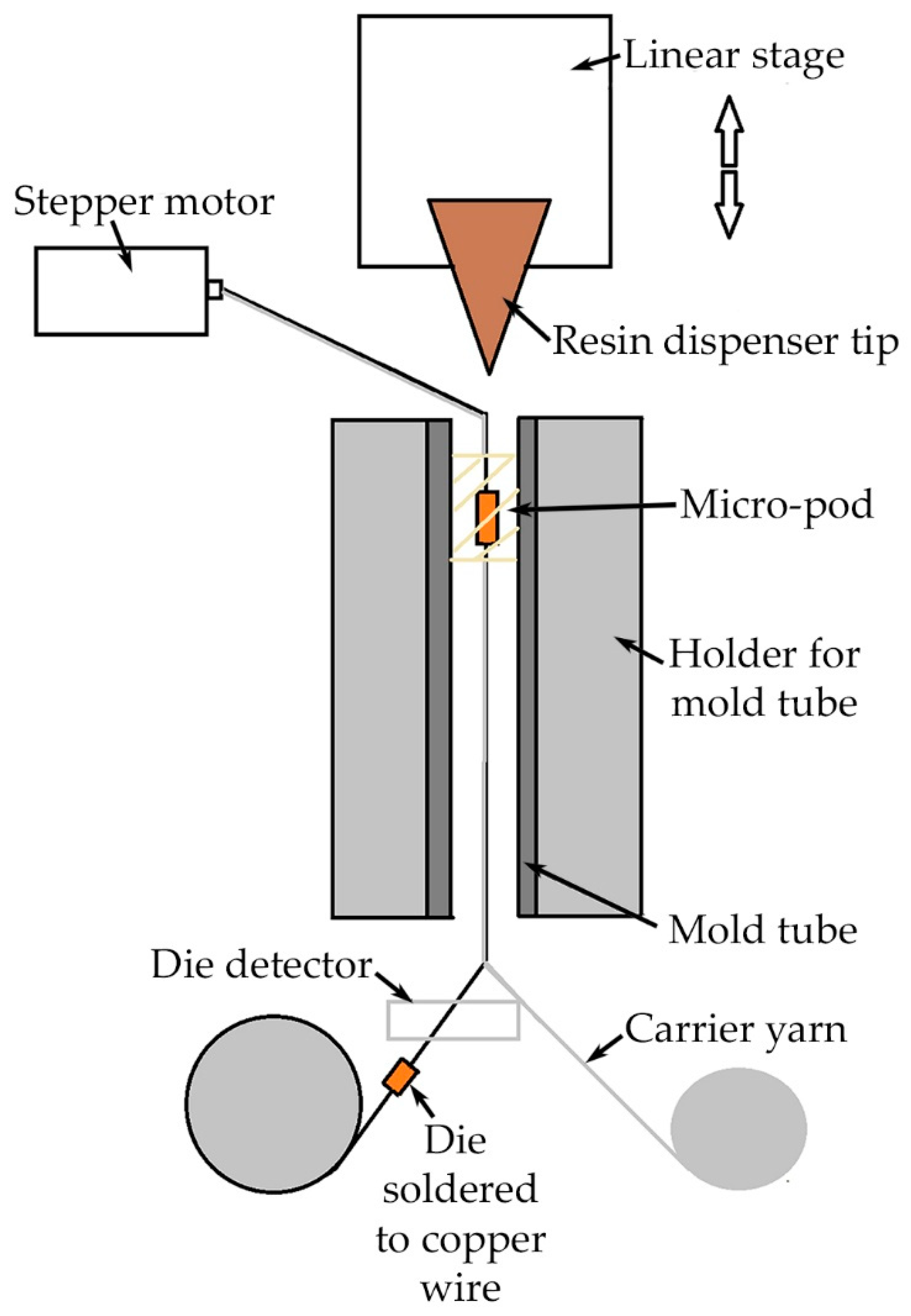
To show the feasibility of automating the encapsulation process, which is critical for commercial production, the encapsulation system was partially automated. A prototype automated encapsulation unit was designed in which the electronic components to be encapsulated were moved into a mold, a pre-determined quantity of resin was dispensed, the resin was UV-cured, and the micro-pod was removed from the mold (completing the encapsulation process). The design illustrated in this paper is based on experimental work in which several designs were investigated. The focus is placed on the design that gave the most consistent results. A schematic of the automated process is shown in Figure 5.
To allow for automation, the location of the soldered die needed to be determined to ensure that resin would only be dispensed once the die was in the correct location. A transmissive fiber sensor unit, FU-58, was used with an amplifier, FS-N11MN (both from Keyence; Milton Keyence, UK). This fiber optic sensor detected changes in light intensity. When the light intensity dropped due to a die arriving between the two parts of the fiber optic sensor, the voltage dropped, so a signal was sent to the encapsulation unit. The signal was interpreted using a LabView program (Version 14; National Instruments, Newbury, UK). The sensor detected the soldered die inside the transparent mold tube, at the point at which encapsulation took place. The minimum detectable object was 0.005 mm2, which was adequate for all package die sizes of interest at this time.
Computer controlled elements were used to automate the encapsulation process. The resin dispenser unit was mounted onto a motorized linear translation stage with an integrated controller (LTS 15; Thorlabs, Ely, UK). This enabled the resin dispenser to be moved vertically to a specific encapsulation point. The linear translation stage provided 150 mm of linear travel with a maximum vertical velocity of 3 mms−1. The force applied by the stepper motor ensured that the linear translation stage remained fixed when no power was supplied, so that a brake did not need to be employed to keep the stage in position. This would not have been the case if a DC (direct current) servo motor was used. The linear translation stage featured an integrated electronic controller that could be controlled using a PC or manually. The stage was calibrated by the manufacturer, giving a typical error of ±4.0 µm when moving over ±20.0 µm travel.
A second set of motors was used to move the copper wire (with attached, soldered electronic components). A stepper motor (ISM 7411E; National Instruments Corporation (U.K.) Ltd., Newbury, UK) was chosen to drive the soldered component to a specific point where the encapsulation process could take place. This stepper drive motor had micro-step emulation and an integrated encoder, and was chosen as it could give a feedback signal to the driving software and therefore increase the accuracy of the movement. An Ethernet communication port controlled the motor via LabVIEW.
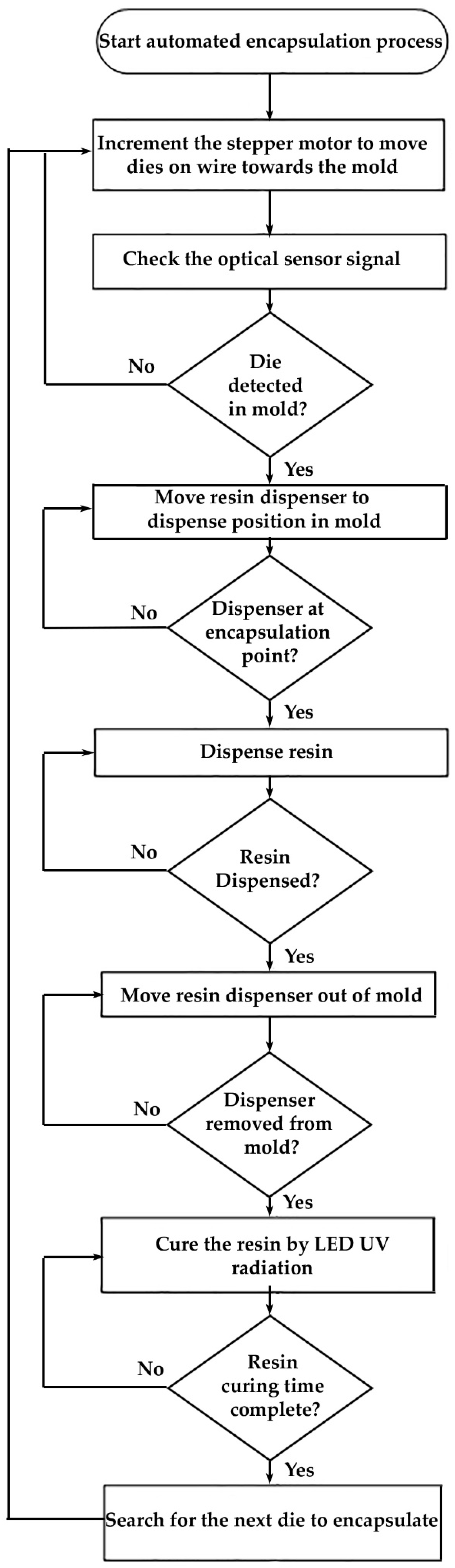
Process Control
The automated encapsulation process was controlled and monitored by a LabView program, which controlled the sequence task as illustrated in the flow chart in Figure 6. The process consisted of the following steps: Following detection of the die, once the electronic component arrived at the encapsulation point in the mold, the stepper motor stopped and the linear stage moved the dispenser until the dispenser tip reached the encapsulation point where the soldered die was located. Resin was then dispensed. The linear stage was used to move the dispenser up again to avoid curing the resin within the dispenser’s tip. The LED UV light source was used to cure the dispensed resin in the mold. The process was then repeated to encapsulate the next die.
2.8. Tensile Testing
The solder joints created in the first stage of production were expected to be the weakest point in the ensemble. The encapsulation process was expected to substantially increase the soldered joint strength against mechanical stresses. Tensile tests were carried out to establish the changes in tensile strength of the construction at each stage of production. The zwickiLine tensile tester was used, working to standard ASTM E8 [28], which related to ‘Standard Test Methods for Tension Testing of Metallic Materials’. The test speed was reduced to 50 mm min−1 to enable testing of the solder joints included within the E-yarn. Five samples were measured from each stage of the E-yarn production process:
- Bare semiconductor dies soldered to copper wire;
- Encapsulated dies, with carrier yarn included within the encapsulation;
- Completed E-yarn, with a textile outer covering around an encapsulated die.
The tensile forces required to break each sample were compared.
3. Results
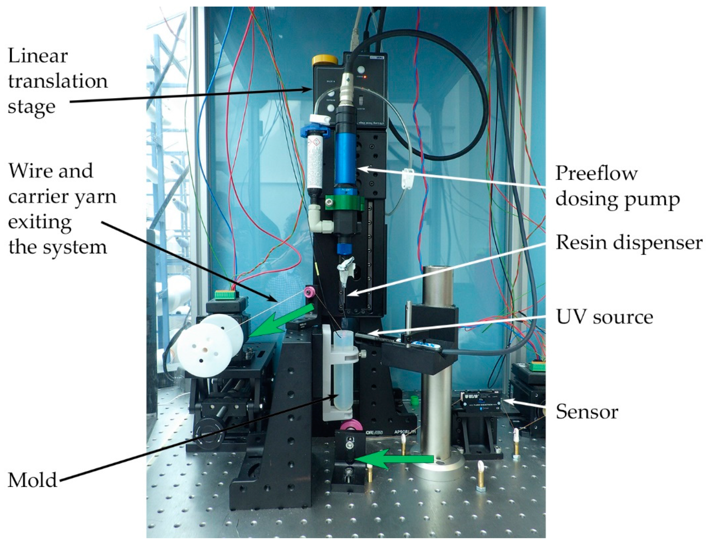
A method was developed to encapsulate package dies on flexible wire, with the process automated using the machinery shown in Figure 7. This shows copper wire and carrier yarn being fed through a sensor and into the bottom of the mold, in which the encapsulation is carried out. The system for injecting resin is directly above the mold, and the UV light guide points to the mold. It was found that a dispensed micro-dot of resin could flow into the tube that formed the mold, rather than being retained where the dispenser injected it. The requirement for resin to flow into the tube, but not fall straight through, also placed a maximum limitation on the diameter of the mold, which was required to hold the liquid resin inside until curing was complete. The chosen electronic components, such as package LEDs and thermistors, were small enough (1.0 × 0.5 × 0.5 mm) to be encapsulated within a 1.27 mm internal-diameter mold.
The method of detecting the presence of a package die to initiate the encapsulation process was achieved with an accuracy of 98% for thermistors and 87% for LEDs. The sensitivity and accuracy of the process depended on the color, reflectivity, size, and shape of the component. The transparent lenses of the LEDs made detection by changes in light intensity more difficult. The angle at which the die arrived at the sensor also affected the detection ability. The front or back of the die facing the sensor was likely to lead to detection, whilst the side of a die was less likely to be detected.
3.1. Fourier Transform Infra-Red (FTIR) Analysis of UV Curing Times
Fourier transform infra-red (FTIR) analysis was performed on sample micro-pods that had been cured for 10 s, 20 s, 30 s, and 50 s by exposure to the 385 nm UV light source. Figure 8 shows transmission spectra for the samples cured for 10 s and 50 s. The curves for the samples cured for 20 s and 30 s were very similar to that for the sample cured for 10 s, so are omitted from Figure 8 for clarity. The peaks of all the analyzed samples are similar to spectra found in the literature for acrylated urethane resins [29]. The spectra in Figure 8 are all similar, implying that full curing of the resin had occurred in all cases. It was therefore acceptable to use a 10 s curing time for a sample of this size, and possibly shorter exposure times may also be appropriate. It was interesting to note that for 50 s of curing (the green line on the graph), there was some reduction in the trough at 1722 cm−1. This indicated over-curing as the literature states that the number of double bonds (C=C) at 1635 cm−1 and 810 cm−1 decrease when over-curing occurs [29]. Over-curing of the resin can affect the structural and optical properties of the resin. Over-curing is to be avoided, as this may change the mechanical properties and optical characteristics of the resin, for example, by causing yellowing. Minimizing the UV curing time for encapsulation had two advantages: Increased speed of encapsulation and prevention of UV degradation of the micro-pods.
3.2. Force Required to Extract Micro-pods from the Mold
Two mold materials were explored in this work (silicone and PTFE), with the internal surfaces of both materials assessed using a scanning electron microscope. Figure 9 shows the internal surfaces of the tubing made from (a) PTFE and (b) silicone. There are clear structural differences between the two surfaces, with the surface of the PTFE tube appearing much rougher than that of silicone at 10,000 times magnification. It was undesirable for the resin to stick within the mold, as this would increase the tension required to remove the micro-pod after curing, increasing the likelihood of a breakage occurring. Both mold materials were tested for ease of removal of a micro-pod from a mold. It was found that the carrier yarn stuck to the wall of the silicone tube during molding, rather than staying within the encapsulant. It was possible that the rougher surface of the PTFE could provide less points of contact area for the cured resin micro-pod to contact, especially if the resin shrank on curing. PTFE was therefore chosen as the mold material, despite its rougher appearance.
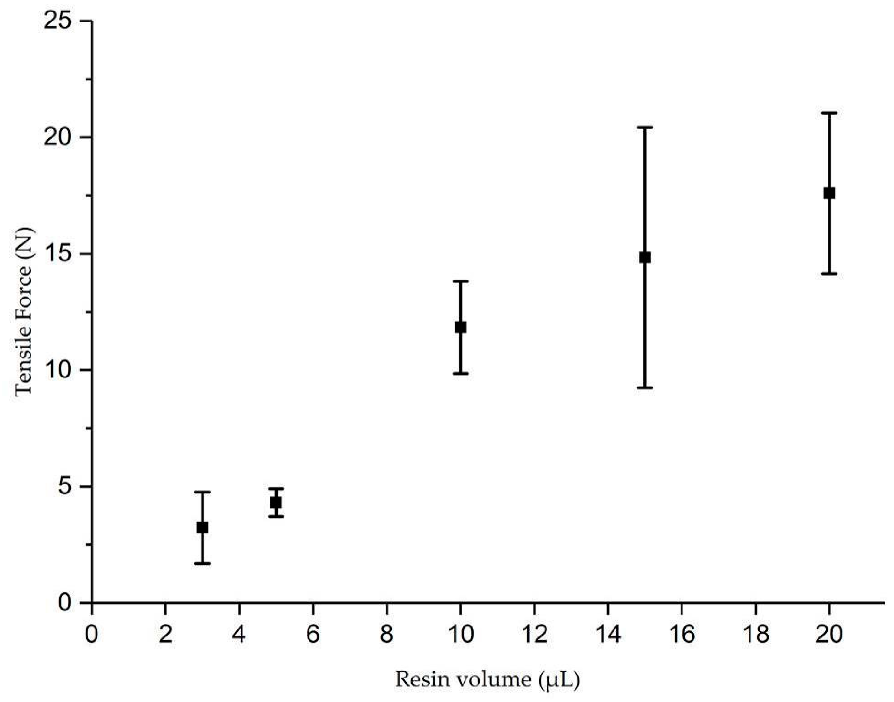
The force required to pull micro-pods from the PTFE mold was subsequently assessed using tensile testing. Figure 10 shows the force required to extract micro-pods from the mold after curing the resin inside a 1.27 mm PTFE tube. The increasing values of tensile force in Figure 10 shows that increasing volumes of resin, which led to increased micro-pod lengths (from 3.9 to 15.8 mm), and therefore contact area, required an increased force to be applied to remove the cured resin from the PTFE tube. The tensile force should not exceed the breaking force of the carrier yarn, which was known to be between 26.2 and 27.6 N [21]. The graph in Figure 10 shows that all micro-pods under investigation could be removed from the mold tube by exerting forces below these values, but further increases in the volume of resin or the diameter of the tube could lead to the force required to remove the micro-pod from the mold exceeding the carrier yarn strength. The results also indicated that the main force required to remove the micro-pod from the tube was a static force: The force required to initiate motion [30]. Little kinetic force [30] was required to maintain motion after this.
3.3. Tensile Testing of E-yarn Components
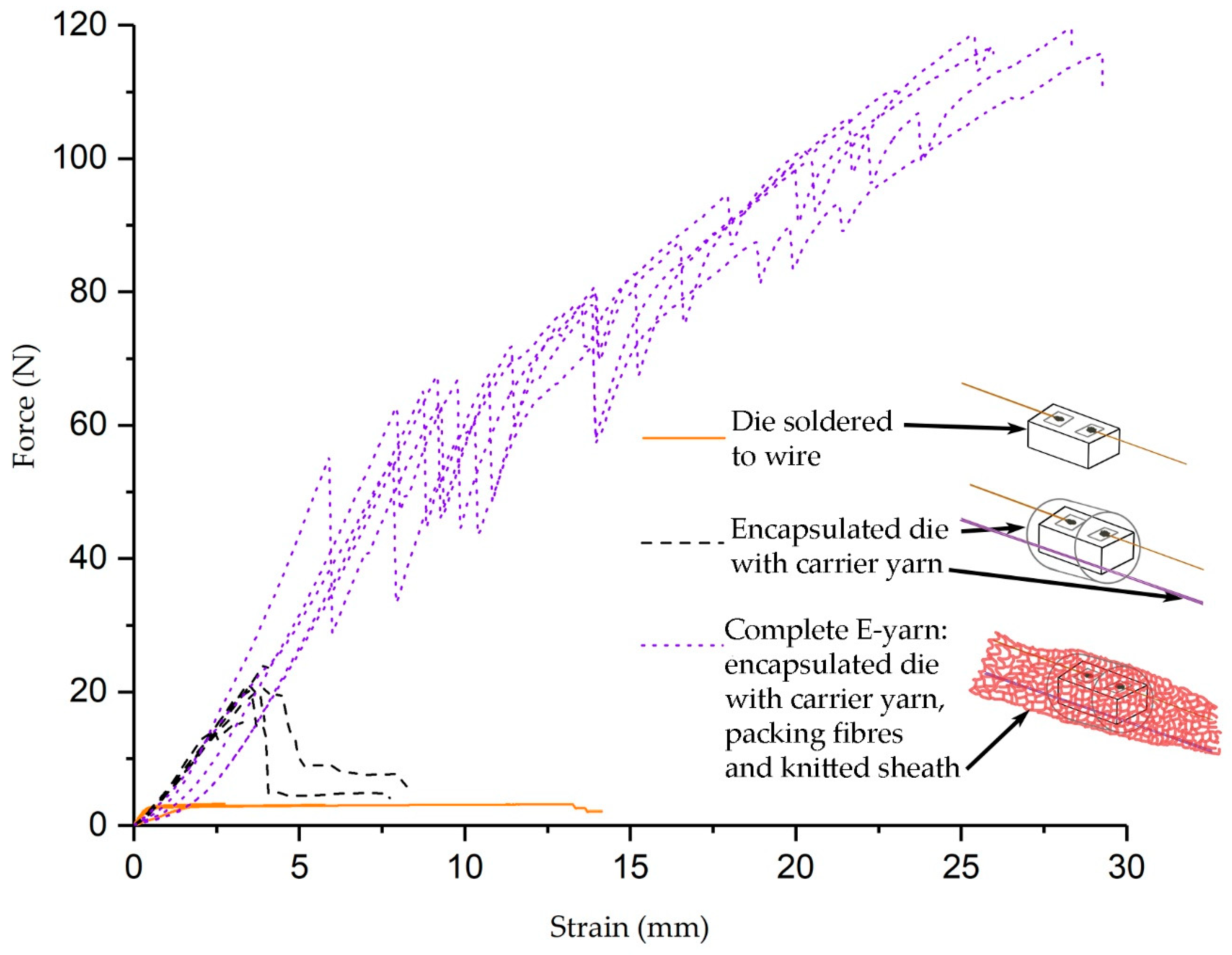
As a final validation of the influence of the encapsulation process, the tensile properties of the encapsulated yarn were compared with those of soldered, un-encapsulated components. Tensile tests were performed on five samples of un-encapsulated dies; five encapsulated dies; as well as five completed E-yarns containing encapsulated dies with carrier yarn, within knitted sleeves. The results are shown in Figure 11. The solid lines at the base of the graph show that un-encapsulated dies soldered onto wire had a low tensile strength with maxima between 2.72 and 3.21 N. Two of the five specimens broke after elongation of the copper wire rather than by fracture of the solder joints between the die and the wire. This is shown by the solid lines that extend along the x-axis of the graph, as the ductile copper extended before breaking. Encapsulating the dies within micro-pods increased the tensile strength to 15.01 to 23.94 N, as shown by the dashed lines on the graph. Encapsulation of the soldered joints, as well as carrier yarns included within the micro-pods, increased the tensile strength of these specimens. The completed E-yarn had a much greater tensile strength, as indicated by the dotted lines on the graph, showing initial breaking forces from 54.93–67.46 N. The use of both the carrier yarn and an outer, knitted sleeve greatly increased the breaking strength of the construction. The E-yarn sleeve was manufactured from eight individual polyester yarns plus packing yarns. The jagged pattern of breakage is likely due to fiber-fiber friction between the packing yarns within the construction. The knitting process brought these yarns together, creating a structure with greater tensile strength than that of the individual textile yarns that made up the construction. The single strands of copper and Vectran™ at the core of the E-yarn had a lower tensile strength. (Vectran™ yarn has been shown previously to have a tensile strength of 23–28 N [21].) The function of the micro-pod was not to provide additional tensile strength, but to protect the die and solder joints against impact and moisture ingress, so the outer sleeve was important in increasing the overall tensile strength.
4. Discussion
Ultimately, an encapsulation unit was designed and constructed, suitable for automated encapsulation of semiconductor dies that had been soldered to wire. This enabled fast, repeated encapsulation of dies soldered to copper wire. The design of the mold in which the micro-pod was formed was key to this process. The design was optimized for 0402 metric package dies measuring 0.5 × 0.5 × 1.0 mm, for which a 1.27 mm internal diameter tube was used as a mold. Since the diameter of the tube was fixed, the volume of resin dispensed, in addition to the size of the component, determined the finished length of the encapsulation. One method of incorporating complex electronic circuits into a yarn is to use flexible Kapton strips as a substrate (as recently reported in the literature [31,32]). This would require micro-pods with lengths from 10 mm up to at least 50 mm. The removal of longer micro-pods from the mold requires tensile forces that exceed the strength of the carrier yarn, so further development of the methodology is required. Further work is also required to investigate the effects of altered mold sizes for smaller and larger dies. The use of a thinner tube to encapsulate dies smaller than the 0402 metric package size used in this work may affect the flow of resin. Larger dies, requiring greater tube diameters, may require alterations to the design to prevent resin from flowing out of the tube before curing.
The prototype automated encapsulation unit described in this work offered a substantial improvement over the manual process previously used to fabricate E-yarns, substantially increasing the speed of the process. This technology is suitable for encapsulation of small electronic dies, such as 0402 metric package dies. This will help lead the way towards larger volume production of E-yarn, which is a critical step towards future commercialization and a greater uptake of the technology.
The E-yarns produced using the encapsulation process were designed to be incorporated into fabric using knitting and weaving machinery. The feasibility of this was demonstrated by inserting E-yarns containing thermistors into knitted textile thermographs [33], and by weaving, using E-yarns containing photodiodes in the weft of woven structures [34]. An important function of the micro-pods formed using the encapsulation unit was to protect the package dies from moisture ingress. Wash trials involving machine washing and tumble drying were carried out on five LED-yarns [35], and on photodiode yarns [34]. Both tests demonstrated that micro-pods formed during the encapsulation process can protect the enclosed package dies from moisture ingress that would lead to failure. Failures were observed at the interface between the copper wire and the micro-pod [34].
5. Conclusions
The manufacture of E-yarn requires the creation of resin micro-pods. These surround package dies that have been soldered to copper wire, protecting the die and solder joints against abrasion and moisture ingress. A prototype, automated encapsulation unit was developed. This included a mold with an inner PTFE tube, in which micro-pods were formed and underwent UV-curing. The materials and construction of the mold were chosen to enable formation, curing, and removal of the resin micro-pod. A Vectran™ carrier yarn with a high tensile strength was placed alongside the copper wire, with a portion of the yarn included within the micro-pod. This added tensile strength to the construction, including when pulling the micro-pod out of the mold. Experiments showed that the force required to pull the micro-pod from the mold was proportional to the volume of resin used to make the micro-pod, with 15 N required to pull a 15 µL micro-pod from a 1.27 mm-diameter mold. FTIR analysis was used to assess whether the resin within the micro-pod was completely cured. This showed that a 10 s cure time was adequate for a cylindrical micro-pod made in a 1.27 mm-diameter mold. Automation of the encapsulation process enabled repeated encapsulation of dies previously soldered to copper wire. Incoming dies were detected 87% to 98% of the time. This process improved the ability to produce the amounts of E-yarn required for further creation of prototype electronic textiles.
Author Contributions
T.D. and T.H.-R. supervised the program of study and provided specialist technical knowledge essential for the completion of this work. M.-N.N. and D.A.H. designed the study, conducted the experiments and performed the data analysis. M.-N.N., T.H.-R. and D.A.H. wrote the paper. All authors discussed the results and contributed to producing the final manuscript.
Funding
This research was funded by the Engineering and Physical Sciences Research Council (EPSRC) grant EP/M015149/1 Novel manufacturing methods for functional electronic textiles.
Acknowledgments
The authors would like to thank our colleagues from the Advanced Textiles Research Group (ATRG) at Nottingham Trent University, who provided insight and expertise that greatly assisted the research, especially Ioannis Anastasopoulos, Carlos Oliveira and Richard Arm. M.-N.N. thanks CARA for their support, sponsorship and financial support. The authors would also like to thank Kathryn Kroon for her assistance in acquiring the SEM images shown in Figure 9.
Conflicts of Interest
The authors declare no conflict of interest. The funders had no role in the design of the study; in the collection, analyses, or interpretation of data; in the writing of the manuscript, or in the decision to publish the results.
References
- Park, S.; Jayaraman, S. Smart Textiles: Wearable electronic Systems. MRS Bull. 2003, 28, 585–591. [Google Scholar] [CrossRef]
- Stoppa, M.; Chiolerio, A.; Stoppa, M.; Chiolerio, A. Wearable Electronics and Smart Textiles: A Critical Review. Sensors 2014, 14, 11957–11992. [Google Scholar] [CrossRef] [PubMed] [Green Version]
- Fernández-Caramés, T.; Fraga-Lamas, P.; Fernández-Caramés, T.M.; Fraga-Lamas, P. Towards The Internet-of-Smart-Clothing: A Review on IoT Wearables and Garments for Creating Intelligent Connected E-Textiles. Electronics 2018, 7, 405. [Google Scholar] [CrossRef]
- Fairs, M. Bono’s Laser Stage Suit by Moritz Waldemeyer. Available online: https://www.dezeen.com/2010/02/28/bonos-laser-stage-suit-by-moritz-waldemeyer/ (accessed on 20 December 2018).
- Castano, L.M.; Flatau, A.B. Smart fabric sensors and e-textile technologies: A review. Smart Mater. Struct. 2014, 23, 053001. [Google Scholar] [CrossRef]
- Weng, W.; Chen, P.; He, S.; Sun, X.; Peng, H. Smart Electronic Textiles. Angew. Chem. Int. Ed. 2016, 55, 6140–6169. [Google Scholar] [CrossRef] [PubMed]
- Hughes-Riley, T.; Dias, T.; Cork, C. A Historical Review of the Development of Electronic Textiles. Fibers 2018, 6, 34. [Google Scholar] [CrossRef]
- Mi Pulse Smart Bras for Smart Fitness. Available online: https://www.mi-pulse.com/ (accessed on 17 January 2019).
- The Liten Institute Printed Components. Available online: http://liten.cea.fr/cea-tech/liten/en/Pages/techno Nanotech Components/PrintedComponents.aspx (accessed on 17 January 2019).
- Lind, A.H.N.; Mather, R.R.; Wilson, J.I.B. Input energy analysis of flexible solar cells on textile. IET Renew. Power Gener. 2015, 9, 514–519. [Google Scholar] [CrossRef]
- Takamatsu, S.; Kobayashi, T.; Shibayama, N.; Miyake, K.; Itoh, T. Fabric pressure sensor array fabricated with die-coating and weaving techniques. Sens. Actuators A Phys. 2012, 184, 57–63. [Google Scholar] [CrossRef]
- Wijesiriwardana, R.; Mitcham, K.; Dias, T. Fibre-Meshed Transducers Based Real Time Wearable Physiological Information Monitoring System. In Proceedings of the Eighth International Symposium on Wearable Computers, Arlington, VA, USA, 31 October–3 November 2004; pp. 40–47. [Google Scholar]
- Gopalsamy, C.; Park, S.; Rajamanickam, R.; Jayaraman, S. The Wearable Motherboard?: The first generation of adaptive and responsive textile structures (ARTS) for medical applications. Virtual Real. 1999, 4, 152–168. [Google Scholar] [CrossRef]
- Rein, M.; Favrod, V.D.; Hou, C.; Khudiyev, T.; Stolyarov, A.; Cox, J.; Chung, C.-C.; Chhav, C.; Ellis, M.; Joannopoulos, J.; et al. Diode fibres for fabric-based optical communications. Nature 2018, 560, 214–218. [Google Scholar] [CrossRef]
- Bigham, K.J. Drawn Fiber Polymers: Chemical and Mechanical Features; Zeus Ind. Prod. Ltd.: Orangeburg, SC, USA, 2018. [Google Scholar]
- European Commission. Integrating Platform for Advanced Smart Textile Applications. Available online: https://cordis.europa.eu/project/rcn/95473/factsheet/en (accessed on 16 January 2019).
- Primo1D: The Technology. Available online: http://www.primo1d.com/e-thread/the-technology (accessed on 16 January 2019).
- Zysset, C.; Kinkeldei, T.; Münzenrieder, N.; Petti, L.; Salvatore, G.; Tröster, G. Combining electronics on flexible plastic strips with textiles. Text. Res. J. 2013, 83, 1130–1142. [Google Scholar] [CrossRef]
- Zeng, W.; Shu, L.; Li, Q.; Chen, S.; Wang, F.; Tao, X.-M. Fiber-Based Wearable Electronics: A Review of Materials, Fabrication, Devices, and Applications. Adv. Mater. 2014, 26, 5310–5336. [Google Scholar] [CrossRef] [PubMed]
- Dias, T. Electronically Functional Yarns. Patent WO2016/038342 A1, 17 March 2016. [Google Scholar]
- Hardy, D.A.; Anastasopoulos, I.; Nashed, M.-N.; Oliveira, C.; Hughes-Riley, T.; Komolafe, A.; Tudor, J.; Torah, R.; Beeby, S.; Dias, T. An Automated Process for Inclusion of Package Dies and Circuitry within a Textile Yarn. In Proceedings of the 2018 Symposium on Design, Test, Integration & Packaging of MEMS and MOEMS (DTIP), Roma, Italy, 22–25 May 2018. [Google Scholar]
- Dias, T.; Hughes-Riley, T. Electronically Functional Yarns Transform Wearable Device Industry. R&D Mag. 2017, 59, 19–21. [Google Scholar]
- Minges, M.L. Electronic Materials Handbook: Packaging; CRC Press: Boca Raton, FL, USA, 1989; Volume 1, ISBN 9780871702852. [Google Scholar]
- Srivastava, A.; Agarwal, D.; Mistry, S.; Singh, J. UV curable polyurethane acrylate coatings for metal surfaces. Pigment Resin Technol. 2008, 37, 217–223. [Google Scholar] [CrossRef]
- Decker, C. Contributed papers UV-radiation curing chemistry. Pigment Resin Technol. 2001, 30, 278–286. [Google Scholar] [CrossRef]
- Boyd, R.H.; Phillips, P.J. The Science of Polymer Molecules: An Introduction Concerning the Synthesis, Structure, and Properties of the Individual Molecules that Constitute Polymeric Materials; Cambridge University Press: Cambridge, UK, 1996; ISBN 0521565081. [Google Scholar]
- Dymax Corporation ELECTRONIC ASSEMBLY MATERIALS: 9001-E-V3.5 Product Data Sheet: Multi-Cure® 9001-E-V3.5 Resilient, Clear Encapsulant. Available online: https://www.dymax.com/images/pdf/pds/9001-e-v35.pdf (accessed on 15 November 2018).
- ASTM ASTM E8/E8M-16A Standard Test Methods for Tension Testing of Metallic Materials. 2016. Available online: https://www.astm.org/Standards/E8.htm (accessed on 25 September 2018).
- Kunwong, D.; Sumanochitraporn, N.; Kaewpirom, S. Curing behavior of a UV-curable coating based on urethane acrylate oligomer: The influence of reactive monomers. Songklanakarin J. Sci. Technol. 2011, 33, 201–207. [Google Scholar]
- Israelachvili, J.N.; Chen, Y.-L.; Yoshizawa, H. Relationship between adhesion and friction forces. J. Adhes. Sci. Technol. 1994, 8, 1231–1249. [Google Scholar] [CrossRef]
- Li, M.; Tudor, J.; Liu, J.; Komolafe, A.; Torah, R.; Beeby, S. The thickness and material optimization of flexible electronic packaging for functional electronic textile. In Proceedings of the 2018 Symposium on Design, Test, Integration & Packaging of MEMS and MOEMS (DTIP), Roma, Italy, 22–25 May 2018; pp. 1–6. [Google Scholar]
- Li, M.; Tudor, J.; Torah, R.; Beeby, S. Stress Analysis and Optimization of a Flip Chip on Flex Electronic Packaging Method for Functional Electronic Textiles. IEEE Trans. Compon. Packag. Manuf. Technol. 2018, 8, 186–194. [Google Scholar] [CrossRef]
- Lugoda, P.; Hughes-Riley, T.; Morris, R.; Dias, T. A Wearable Textile Thermograph. Sensors 2018, 18, 2369. [Google Scholar] [CrossRef]
- Satharasinghe, A.; Hughes-Riley, T.; Dias, T. Photodiodes embedded within electronic textiles. Sci. Rep. 2018, 8, 16205. [Google Scholar] [CrossRef]
- Hardy, D.; Moneta, A.; Sakalyte, V.; Connolly, L.; Shahidi, A.; Hughes-Riley, T. Engineering a Costume for Performance Using Illuminated LED-Yarns. Fibers 2018, 6, 35. [Google Scholar] [CrossRef]
Figure 1.
(a) A schematic showing the E-yarn (electronic yarn) structure, with an LED (light-emitting diode) protected by a micro pod and surrounded by a knitted sheath. (b) A completed E-yarn containing an LED (illuminated) shown at 30x magnification.
Figure 1.
(a) A schematic showing the E-yarn (electronic yarn) structure, with an LED (light-emitting diode) protected by a micro pod and surrounded by a knitted sheath. (b) A completed E-yarn containing an LED (illuminated) shown at 30x magnification.

Figure 2.
The main processes in the production of E-yarn. The dashed lines represent an optional stage: Twisting of textile yarns around the wire and encapsulated dies.
Figure 2.
The main processes in the production of E-yarn. The dashed lines represent an optional stage: Twisting of textile yarns around the wire and encapsulated dies.

Figure 3.
A carrier yarn included within the encapsulation of a semiconductor soldered onto copper wire, at 50× magnification.
Figure 3.
A carrier yarn included within the encapsulation of a semiconductor soldered onto copper wire, at 50× magnification.

Figure 4.
(a) A schematic showing an encapsulated die being pulled from the mold. (b) Diagram showing the area over which friction forces will act when pulling a die from the mold.
Figure 4.
(a) A schematic showing an encapsulated die being pulled from the mold. (b) Diagram showing the area over which friction forces will act when pulling a die from the mold.

Figure 5.
Schematic illustration of the automated encapsulation unit, showing die detection before entering the silicone mold; and a completed micro-pod surrounding an encapsulated die about to exit from the mold.
Figure 5.
Schematic illustration of the automated encapsulation unit, showing die detection before entering the silicone mold; and a completed micro-pod surrounding an encapsulated die about to exit from the mold.

Figure 6.
Flowchart illustrating the sequence of logic steps followed by the LabView program to enable the automated encapsulation of components.
Figure 6.
Flowchart illustrating the sequence of logic steps followed by the LabView program to enable the automated encapsulation of components.

Figure 7.
A photograph of the encapsulation system. The main components are labelled, and the large, green arrows show the direction of travel through the system of the copper wire with attached sensors.
Figure 7.
A photograph of the encapsulation system. The main components are labelled, and the large, green arrows show the direction of travel through the system of the copper wire with attached sensors.

Figure 8.
FTIR results from resin samples cured for 10 and 50 s.

Figure 9.
SEM images of the inner surface of the encapsulation mold materials at 10,000 times magnification: (a) PTFE (polytetrafluoroethylene) tube. (b) Silicone tube.
Figure 9.
SEM images of the inner surface of the encapsulation mold materials at 10,000 times magnification: (a) PTFE (polytetrafluoroethylene) tube. (b) Silicone tube.

Figure 10.
Tensile forces required to pull a micro-pod from a mold as a function of the quantity of resin used to encapsulate a semiconductor in a 1.27 mm-diameter PTFE tube.
Figure 10.
Tensile forces required to pull a micro-pod from a mold as a function of the quantity of resin used to encapsulate a semiconductor in a 1.27 mm-diameter PTFE tube.

Figure 11.
Tensile test results for samples of soldered dies; encapsulated dies with carrier yarn; and E-yarn with a knitted sheath surrounding encapsulated dies with carrier yarn and packing fibers.
Figure 11.
Tensile test results for samples of soldered dies; encapsulated dies with carrier yarn; and E-yarn with a knitted sheath surrounding encapsulated dies with carrier yarn and packing fibers.

© 2019 by the authors. Licensee MDPI, Basel, Switzerland. This article is an open access article distributed under the terms and conditions of the Creative Commons Attribution (CC BY) license (http://creativecommons.org/licenses/by/4.0/).
Share and Cite
MDPI and ACS Style
Nashed, M.-N.; Hardy, D.A.; Hughes-Riley, T.; Dias, T. A Novel Method for Embedding Semiconductor Dies within Textile Yarn to Create Electronic Textiles. Fibers 2019, 7, 12. https://0-doi-org.brum.beds.ac.uk/10.3390/fib7020012
AMA Style
Nashed M-N, Hardy DA, Hughes-Riley T, Dias T. A Novel Method for Embedding Semiconductor Dies within Textile Yarn to Create Electronic Textiles. Fibers. 2019; 7(2):12. https://0-doi-org.brum.beds.ac.uk/10.3390/fib7020012
Chicago/Turabian StyleNashed, Mohamad-Nour, Dorothy Anne Hardy, Theodore Hughes-Riley, and Tilak Dias. 2019. "A Novel Method for Embedding Semiconductor Dies within Textile Yarn to Create Electronic Textiles" Fibers 7, no. 2: 12. https://0-doi-org.brum.beds.ac.uk/10.3390/fib7020012
Note that from the first issue of 2016, this journal uses article numbers instead of page numbers. See further details here.