Energy-Efficient Architecture for CNNs Inference on Heterogeneous FPGA


1
Department of Informatics, Modeling, Electronics and System Engineering, University of Calabria, 87036 Rende, Italy
2
Department of Mechanical, Energy and Management Engineering, University of Calabria, 87036 Rende, Italy
*
Author to whom correspondence should be addressed.
J. Low Power Electron. Appl. 2020, 10(1), 1; https://0-doi-org.brum.beds.ac.uk/10.3390/jlpea10010001
Submission received: 6 December 2019
/
Revised: 20 December 2019
/
Accepted: 21 December 2019
/
Published: 24 December 2019
(This article belongs to the Special Issue Low-Power FPGA Designs for Next-Generation Artificial Intelligence Applications)
Abstract
:Due to the huge requirements in terms of both computational and memory capabilities, implementing energy-efficient and high-performance Convolutional Neural Networks (CNNs) by exploiting embedded systems still represents a major challenge for hardware designers. This paper presents the complete design of a heterogeneous embedded system realized by using a Field-Programmable Gate Array Systems-on-Chip (SoC) and suitable to accelerate the inference of Convolutional Neural Networks in power-constrained environments, such as those related to IoT applications. The proposed architecture is validated through its exploitation in large-scale CNNs on low-cost devices. The prototype realized on a Zynq XC7Z045 device achieves a power efficiency up to 135 Gops/W. When the VGG-16 model is inferred, a frame rate up to 11.8 fps is reached.
1. Introduction
Nowadays, Convolutional Neural Networks (CNNs) are exceptionally popular for being able to exceed human accuracy in plenty of applications, ranging from recognition tasks [1] such as face detection [2], object classification [1], text understanding [3] and speech recognition [4], to autonomous driving electric cars [5] and Internet of Things (IoT) devices [6]. In such a scenario, researchers have recently focused their attention on the design of hardware accelerators for deep CNNs able to operate in real time with limited power consumption and costs. However, state-of-the-art deep CNNs [7,8,9,10] perform hundreds of millions of operations on a considerable amount of data, thus leading to several computation and memory issues that leave the design of hardware accelerators still a challenge.
With the aim of saving energy consumption and resources occupancy without significantly penalizing the overall quality, several studies [1,11,12,13,14] have proposed the quantization of both network parameters and feature maps for many state-of-the-art CNN models. The benefits of such a strategy are impressive. Just as an example, let us examine what the consequence is of reducing data precision on basic arithmetic building blocks. An 8-bit fixed-point adder dissipates 33% (3.4%) of the energy consumed by a 32-bit fixed-point (floating-point) adder, requiring 3.8 × (116×) less area. The advantages offered by the reduced precision are even more evident in the case of multiplications. In fact, an 8-bit fixed-point multiplier consumes only 6.45% (5.4%) of the energy dissipated by a 32-bit fixed-point (floating-point) multiplier, spanning 12.4 × (27.5×) less area [15,16].
Exploring quantization and approximation strategies makes it possible to design efficient accelerators suitable for both Application-Specific Integrated Circuits (ASIC) [17] and Field-Programmable Gate Array (FPGA) [18] hardware platforms. Although the efficiency of FPGA platforms in the implementation of artificial neural networks has already been proven [19,20], modern heterogeneous FPGA Systems-on-Chips (SoCs) are often preferred when dealing with deep convolutional neural networks, since they offer a good balance in terms of performance, cost and power efficiency. Indeed, both Xilinx [21,22] and Intel [23,24] SoC-FPGAs merge the flexibility of software routines running on a general-purpose processor with the advantages of special-purpose parallel hardware architectures. The former can be developed by exploiting optimized software libraries, as well as the support of an operating system, to manage communication with possible system peripherals. The latter are typically needed to implement time- and/or energy-critical operations, which represent an overhead for the application. This allows energy efficiencies higher than traditional GPUs to be achieved [25]. In the literature, several FPGA-based designs have been presented to accelerate the inference of 16- [26,27,28,29] and 8-bit [30,31] fixed-point quantized CNNs. However, while some of them [28,29,30,31] were optimized to achieve high performanc by directly increasing the level of parallelism with which feature maps are processed, others [26,27] were mainly oriented towards low-power applications.
This paper presents a power-efficient heterogeneous embedded system purposely designed for real-time inference of large-scale CNNs. The proposed architecture is structured to be implemented within virtually any FPGA-based SoCs, enabling competitive speed and energy performances to also be achieved when targeting low-end devices. As a case study, two prototypes were realized based on the SoCs of the Xilinx Zynq-7000 family. They mainly differ from each other with respect to the adopted computational parallelism level. The cheapest design uses 220 DSPs and performs 95.5 Gops/s at the 150 MHz running frequency. Conversely, the high-performance implementation achieves an effective power efficiency of 135 Gops/W at the 167 MHz running frequency by using 880 DSPs. It shows a more favorable speed-power trade-off than several recent competitors. Both implementations were validated in accelerating the large-scale VGG-16 [7] CNN. In this case, the novel embedded systems exhibited end-to-end frame rates of 2.65 and 11.8 fps, which significantly outperform state-of-the-art implementations based on the same embedded platforms and well suit pervasive low-cost IoT applications.
2. Background and Motivations
One of the most representative examples of the application of deep CNNs is the task of image classification, which allows the extraction of features from images and their classification into a certain group of categories. Generally speaking, a deep CNN consists of a certain number of cascaded convolutional layers (CONVs), each structured as shown schematically in Figure 1a. The generic CONV layer receives a set of M 2D arrays of input data, named input feature maps (ifmaps), and produces a set of N 2D output feature maps (ofmaps). It is worth noting that, to furnish the generic ofmap, each ifmap is filtered using a distinct 2D convolution kernel, and the M results obtained in this way are combined by means of a pixel-wise addition. The N intermediate ofmaps are further processed by applying a non-linear function, such as the rectified linear unit (ReLU) [32], which sets negative values to zero, while keeping positive values unchanged. Afterwards, normalization or quantization and sub-sampling are optionally performed. The resulting N ofmaps are then inputted to the subsequent CONV, which will produce its own set of ofmaps. The Mc ofmaps produced by the last convolutional layer are finally processed by the classifier, and typically implemented by the so-called fully connected (FC) layers. As schematized in Figure 1b, the generic FC layer also applies filters on the ifmaps, but, in this case, the filters and the ifmaps have the same size. For each ifmap a matrix product (MP) is computed; the resulting Mc matrix products are added and then processed by the ReLU module to furnish one element of the 1 × 1 × Nc ofmap.
Each deep CNN model exploits differently cascaded CONV and FC layers to achieve even greater accuracy [7,8,9,10]. However, as discussed in [33], in state-of-the-art deep CNNs, CONVs consume most of the computational time, thus becoming one of the most critical tasks responsible for limiting reachable speed performances. For this reason, the design of hardware parallel convolutional engines suitable for the inference of deep CNNs in high-performance low-power applications has recently received a great deal of attention [26,27,28,29,30,31,34]. The most exploited design techniques aim to boost the achievable performances by increasing the level of parallelism with which data is processed [28,29,30,31,34]. Indeed, as is visible in Figure 1a, most of the computations involved in a convolutional layer are independent from each other, offering the possibility of parallelizing the operations within the kernel and across both ifmaps and ofmaps. Although such an approach leads to a significant increase in speed, it also introduces a detrimental effect on the area occupancy and the power consumption that, in some cases, leads the hardware design effort to be in vain [30,34]. Conversely, hardware accelerators oriented towards minimizing energy dissipation typically exhibit low performances [26,27].
The exploitation of fixed-point representation and quantization techniques to improve throughput and power performances of hardware CNN accelerators has been widely discussed [11,12,13,14]. Previous works have variously exploited the 16- [26,27,28,29,34] and 8-bit [16,30,31,35,36,37] reduced precisions on both feature map values and parameters to realize efficient FPGA-based designs. The energy-efficient CNN accelerator proposed in [27] adopts a 16-bit representation to enable on-chip storage of parameters and partial results and to reduce power consumption associated with data transfers to/from the external memory. In such a case, a dynamic power less than 500 mW is dissipated at the 150 MHz clock frequency, but the frame rate is limited to just 0.61 fps when running the VGG-16 model [7]. This drawback mainly comes from the strategy adopted to employ DSP slice resources. Indeed, in [27], each DSP slice was used to perform just one multiplication, leading to the internal accumulator being unused and performing the sum of products by a further adder tree structure. Conversely, in [28], 16-bit quantized precision was exploited to save DSPs and to map one product within the 18 × 18-bit embedded multiplier (EM) available within the Stratix [23] and Arria [24] FPGA SoC devices. Despite this optimization, the accelerator presented in [28] required a massive increase in parallelism levels, and also introduced unrolling and tiling operations to achieve a frame rate of 23.1 fps using over 1500 EMs and 2200 on-chip block RAM.
The NullHop accelerator presented in [29] aimed to reduce on-chip memory requirements and to speed up the inference of large-scale CNNs by means of an efficient compression technique. The latter exploits the sparsity of neuron activations in a CNN to produce compressed ifmaps that can be represented with the 16-bit fixed-point format. Therefore, the complete embedded system proposed in [29] benefits from such a quantization for reducing the power consumption related to the data transfers. However, the coding/decoding scheme required on each ifmap limits the overall performances. As an example, when applied to the VGG-16 model [7], only 0.66 frames per second are processed.
Even lower bit-precision can be exploited to further improve speed and/or power performances. In [30,31], 8-bit fixed-point representation was used to reduce, respectively, the area occupancy and the amount of on-chip memory required to store the network parameters and intermediate feature maps produced by the various CONV layers. While the approach described in [30] allows the reduction of the power consumption to just a few Watts, that presented in [31] exhibits a frame rate of 12.2 fps when running the VGG-16 [7]. However, both of these designs are standalone, and they do not take into account the interactions with auxiliary modules always required in embedded systems based on heterogeneous SoCs.
Appropriately reducing the data precision to 8 bits also allows the high-performance DSP blocks to be exploited to realize fast double [16,35,36,37] MAC architectures. Unfortunately, the latter require auxiliary operations to correct the output of each DSP block used to perform multiplications, thus causing detrimental effects on speed performances, resources requirements and power consumption. Furthermore, the architecture proposed in [36] uses a memory access policy that does not allow exploitation of high-performance continuous data streaming for input and output data transfers. Thus, this kind of accelerator cannot be easily integrated within real-time heterogeneous embedded systems.
In [34], a complete embedded system targeting FPGA-based heterogeneous SoC was presented to accelerate both CONV and FC layers through a custom hardware accelerator, implemented within the fabric and the CPU, respectively. This partitioning strategy enabled a frame rate of 5.5 fps to be achieved, along with a power dissipation of about 10 W for the VGG-16 inference. However, in order to feed the convolution engine with a large set of inputs at each clock cycle, on-chip buffers are required. Moreover, to fully exploit the data width of the bus available for communication with the external memory, the authors in [34] doubled the number of DSP slices used, thus furnishing two outputs at once. However, the resulting processing unit appears to be very inefficient. In fact, it performs 169 Gops per second at the 140 MHz running frequency, with the average number of operations per DSP slice equal to just 1.4.
In this paper, we present an efficient embedded system dedicated to the inference of large-scale CNN models and suitable for integration within modern heterogeneous SoCs. In contrast to previous works, the design proposed here focuses on both micro- and system-level aspects to achieve high performance and low power consumption. The designed system architecture is structured to support the efficient Single-Instruction-Multiple-Data (SIMD) paradigm for computing both CONV and FC layers. With this aim, we realized an on-purpose designed buffer architecture able to feed the CONV computing unit properly. Furthermore, specialized software routines exploiting NEON multimedia engine have been developed to accelerate the FC layers elaboration. This approach allows fully exploiting the processing capabilities of such heterogeneous FPGA SoC, significantly improving the overall performance over state-of-the-art CNN accelerators implemented on similar embedded platforms. The design proposed here is highly flexible and portable, and very promising when moving to the next generation of multi-processor SoC (MPSoC) devices, making available more powerful hardware-configurable and software-programmable units.
3. The Proposed SIMD CNN Accelerator
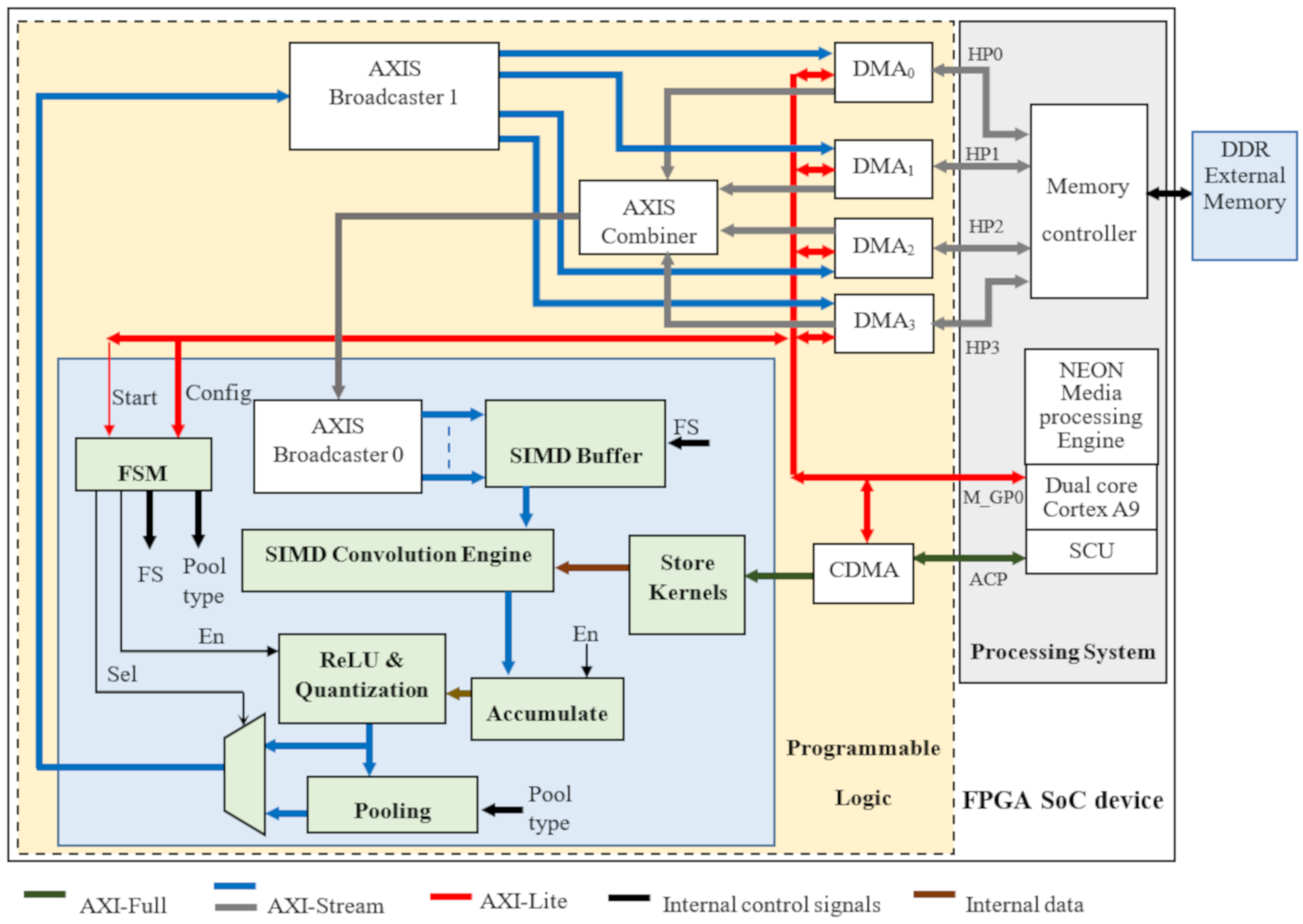
The top-level architecture of the proposed accelerator is depicted in Figure 2. It consists of two main parts: the programmable logic (PL) that accommodates the custom modules performing all the operations involved in a CONV layer, and the processing system used to run software control routines and to execute the FC layers. The SIMD paradigm is exploited to process TM ifmaps in parallel and to produce TN ofmaps contemporaneously. Thus, the generic K × K CONV layer, receiving M ifmaps and producing N ofmaps, is completed within ns = (M/TM) × (N/TN) computational steps performed as follows. The SIMD buffer receives input data through an AXI-stream (AXIS) [38] and, after a latency depending on the number of columns W in the ifmaps, it prepares TM K × K convolution windows for the subsequent SIMD Convolution Engine (CE). The latter is designed to perform double MAC operations by enabling a further intra-feature map parallelism based on a new efficient processing strategy. In the meantime, the module Store Kernels reads the K × K × TM × TN kernel coefficients from the external memory through AXI-Full transactions [38] and delivers them to the SIMD CE, which performs the TM × TN planned convolutions in parallel. The Accumulate module then accumulates the obtained results by exploiting a local memory buffer and finally outputs the intermediate ofmaps. The finite state machine (FSM) orchestrates the activities of all modules, considering the current layer information provided by the PS through an AXI-Lite interface [38], and the intermediate steps already performed. For this purpose, the bidirectional CTRL bus is used. As soon as all the intermediate ofmaps are accumulated, the ReLU & Quantization module is activated; the quantized ofmaps are optionally sub-sampled by the Pooling module and then outputted. Input data and kernel coefficients are 8-bit unsigned and signed fixed-point numbers, respectively. To efficiently exploit the SIMD paradigm, two couples of 8-bit values belonging to two different ifmaps (i.e., ifpt and ifpt+1 with t = 0, 2,..., M − 2) are accommodated within one 32-bit word, ensuring that two adjacent elements of ifpt are interleaved with two adjacent elements of ifpt+1. Data packed in this way are stored in the external memory in the raster order. It is worth pointing out that the proposed architecture is designed to output ofmaps already packed as described above. Therefore, no specific data re-adjustment is required between consecutive convolutional layers. A slightly different strategy is used to store the K × K convolution kernels, which are indeed packed within 64-bit words, ensuring that the coefficients having homologous positions within eight distinct kernels are packed in the same word and transferred from the external memory at the same time.
3.1. Architecture of the SIMD Buffer
The proposed hardware accelerator is made to be able to process in SIMD fashion two adjacent values of each of the TM ifmaps received as input, and to furnish two adjacent values of distinct TN ofmaps. To this end, a window consisting of K × (K + 1) values must be patched over each ifmap to accommodate two adjacent convolution windows. This requires an unconventional buffer stage design. The SIMD reconfigurable buffer depicted in Figure 3 uses TM instances of the internal buffer IBuff, each consisting of K − 1 FIFOs and registers, with being the radius of the convolution window. Each IBuff internally splits the incoming 16-bit data into two pieces of 8-bit data that feed two different pipes: the former consisting of the nr + 1 registers R1, …, Rnr+1, and the other composed of the nr + 2 registers Rnr+2, …, R2nr+2 and Raux. Such an additional register is required to correctly pair incoming values when nr is odd. To better explain why this is necessary, let us consider the example of Figure 4a, which shows the case in which the generic IBuff receives a 4 × 8 ifmap and arranges 3 × 3 convolution windows. It is important to note that, due to the zero padding, the first incoming pair of adjacent values A1 and B1 does not appear in the correct relative position for parallel operation in the two highlighted convolution windows. In fact, A1 in the brown window corresponds to the padding zero value in the blue one, whereas B1 in the brown window corresponds to A2 in the blue one. To guarantee that the incoming data will be multiplied by the correct kernel coefficients, they must be properly recoupled before reaching the FIFO1. This is done through five registers, R1, R2, R3, R4 and Raux, as shown in the timing diagram illustrated in Figure 4b. It is easy to verify that, when nr is even, incoming data are already correctly paired. In this case, the register Raux has no effect. The data-path then goes on through the subsequent FIFOs and registers that furnish data depending on nr, as summarized in Figure 4c, where the symbol ’&’ is used to indicate concatenations of two 8-bit registers.
The module Recognize Borders, shown in Figure 3, establishes whether the central values within the current convolution windows belong to the borders of the ifmaps and, if necessary, as required by the zero padding, it masks appropriate values of the current convolution windows with zeros before being streamed out. It is worth noting that the proposed reconfigurable SIMD buffer also adapts itself to the different ifmaps sizes as they occur when moving from one CONV layer to another. To do this, FIFOs are realized by means of dual-port RAM blocks that are accessed in read and write modes at the addresses RAddr and WAddr, respectively. Both of these addresses are furnished by the module Address Generator, taking into account that the required effective FIFOs depth varies depending on the current CONV layer, based on the FS parameter provided by the external FSM and set as half the ifmap width W. Finally, the output stream to be dispatched to the SIMD CE is generated, taking into account the latency introduced by the buffer and the stride required by the current CONV layer.
3.2. Design of the SIMD CE
The SIMD CE represents the computational core of the system. It is designed to perform parallel MACs on the convolution windows formed by the buffer. In modern FPGAs, such elaborations can be synthesized on high-performance DSP slices, on reconfigurable logic elements, or by using both resources. However, concatenating DSP slices through dedicated fast interconnections allows the highest speed–power efficiency to be achieved. As an example, we observed that the fastest 9-input MAC unit realized by means of reconfigurable resources was 140% slower and consumed 50% more energy than the DSP-based counterpart.
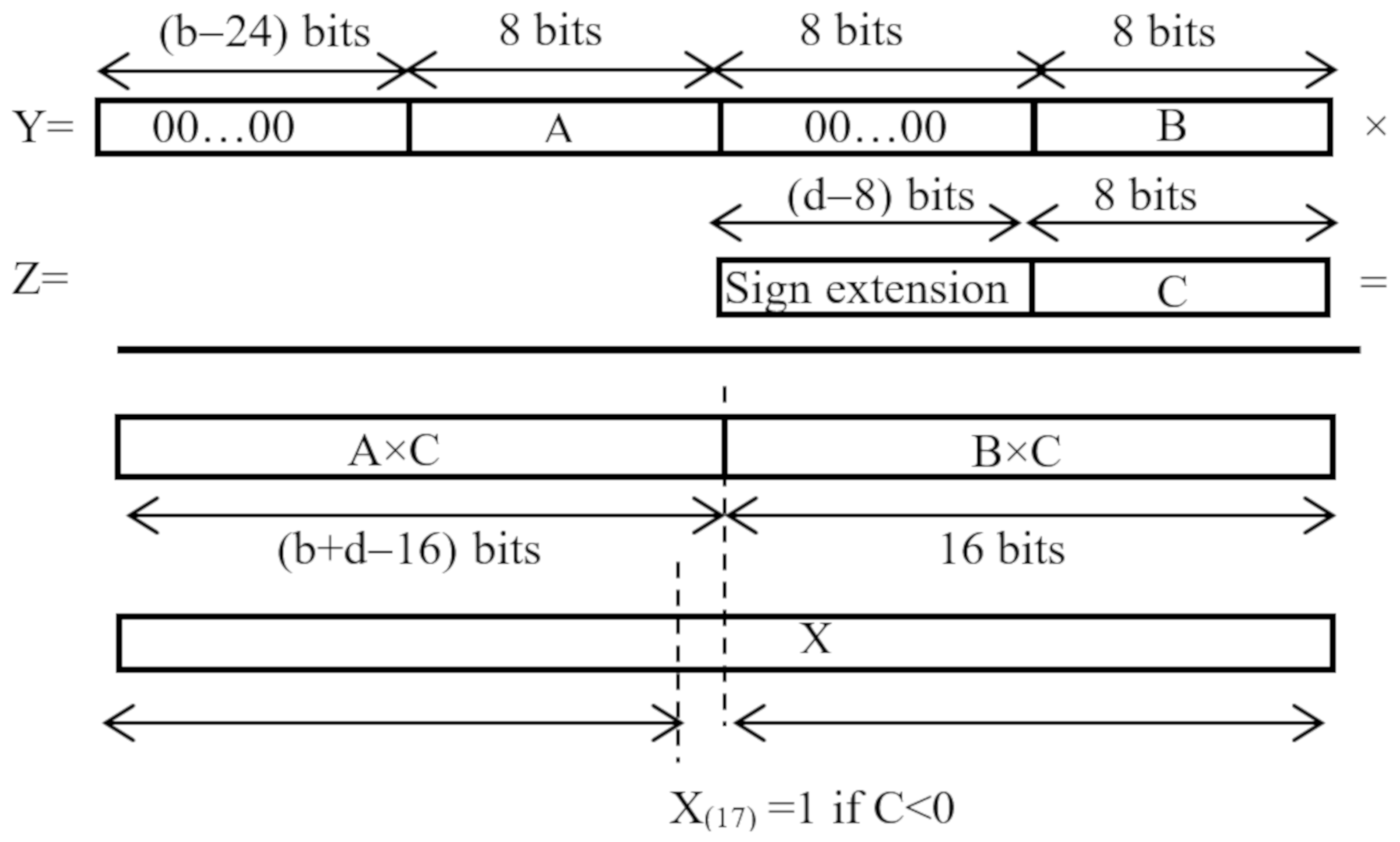
The proposed architecture can be realized using any kind of DSP slice, providing at least one b × d multiplier and one u-bit accumulator (with b ≥ 25, d ≥ 8 and u > 33). However, making the DSPs able to perform parallel MACs operating in SIMD fashion is not a trivial task. Let’s indicate with A = ifpt(h,w) and B = ifpt(h,w + 1) two adjacent packed unsigned elements uploaded from the generic ifmap. With C being the generic signed kernel coefficient, for the above-mentioned purpose, two independent products A × C and B × C have to be computed in parallel. As schematized in Figure 5, the inputs A and B are re-arranged within the b-bit input Y of a DSP interposing eight zero bits to each other and zeroing the remaining MSBs of Y to guarantee that the operand A is always treated as an unsigned value. Conversely, the d-bit operand Z is used to input the sign extended 8-bit coefficient C. When the latter is negative, the DSP applies the 2 s complement notation to the overall result instead of the two separate products, thus necessitating an increment by one of the product A × C to compensate the introduced error. Due to the different data arrangement used, the designs of double MAC (DMAC) engines presented in [16,36,37] address this issue through logic resources external to the DSPs that perform multiplications. This approach negatively affects the computational time, since it breaks the chain of DSPs cascaded along dedicated fast routing resources. In the SIMD CE proposed here, as shown in Figure 5, the products A × C and B × C are accommodated within the (b + d)-bit output of the multiplier occupying the (b + d − 16) MSBs and the 16 LSBs, respectively. Due to this, the correction is done by adding one auxiliary u-bit operand X by using the accumulator internal to the same DSP slice that performs the multiplication. To increment by one the product A × C while leaving B × C unchanged, when C is negative, X must be set to 216, thus asserting only its 17-th bit. Conversely, when C is positive, X must be set to zero. In this way, the cascaded DSPs used to perform the DMACs can complete their operations without encountering breaks along their dedicated fast chain.
The design of the proposed SIMD CE is depicted in Figure 6. It consists of TN Processing Elements (PEs) that compute distinct TN ofmaps in parallel by processing K × K × TM pairs of 8-bit data transferred by the SIMD buffer and the kernel coefficients provided by the module Store Kernels. The module SEPARATE routes the data streamed by the SIMD Buffer to the PEs, whereas the module Generate Out Stream arranges the results as ruled by the AXI4-Stream protocol. As can be seen in Figure 6, the generic PE consists of NDMAC DMACs, each responsible for processing b-bit data through as many DSP slices configured to perform SIMD operations. Each DSP receives one packed b-bit operand and one kernel coefficient C as inputs and computes two parallel 16-bit products A × C and B × C. To perform the subsequent accumulations correctly, each SIMD result is re-arranged over u bits by the module INSERT GUARD BITS. The latter sign extends the 16-bit product B × C to bits, and left-shifts the 16-bit product A × C by positions. In this way, guard-bits are introduced between the two independent products, thus allowing up to accumulations to be performed in SIMD fashion. The u-bit data obtained in this way are then dispatched to the subsequent DSPs configured as accumulators. Further cascaded DSP slices then accumulate the results produced in parallel by the DMACs involved in the generic PE. If u < 64, the two adjacent -bit packed values outputted by the generic PE are separately sign extended to 32 bits; re-arranged within one 64-bit word; and streamed out with the results coming from the other PEs.
Then, as can be seen in Figure 2, either the Accumulate or the ReLU & Quantization module performs further operations. The FSM manages the accumulation of partial results furnished by the SIMD CE at the generic computational step and their storage within on-chip Dual Port RAMs. As the last step, ofmaps are delivered to the ReLU & Quantization module. The latter processes TN ifmaps in parallel, as established by the chosen rectified activation function. The quantized results are finally streamed out towards either the external memory or the Pooling module, which can perform the downsampling by applying either the Max Pooling, or the Average Pooling, or the Stochastic spatial sampling. Such a choice can be dynamically modified via software. The Pooling module produces the first valid result after FS + 1 clock cycles and then furnishes a new output every clock cycle until two consecutive rows of the received ifmap are processed. During the subsequent FS cycles, the circuit just waits for the next downsampling window. Then, a new output value is produced at each clock cycle until two further rows have been processed, and so on.
3.3. Implementation of the Fully Connectd Layers
Most CNN models require a certain number of fully connected layers to produce classifiers. In the proposed system, the FC layers are executed by means of purpose-designed software routines run by the PS. The pseudo code reported in Figure 7 was written exploiting the NEON multimedia engine [39], which supports SIMD and vector floating-point instruction sets. This capability is available within Zynq-7000 [21], Zynq-UltraScale+ [22], Stratix 10 [23] and Arria 10 [24] devices. SIMD and vector instructions, as well as data types, supported by the NEON library, allow eight different computations to be performed in parallel. As an example, it can be seen that type int32 × 4_t is used to define a 128-bit packed word (e.g., vecsum), in which four 32-bit signed integer numbers can be accommodated to be processed in SIMD fashion. The generic FC layer computes the Nc-element array simdsum. To calculate its j-th 32-bit element, the proper kernels coefficients are transferred from the external memory to the 64-bit variable Coeff through the appropriate reading instruction. The uploaded data is re-arranged as eight distinct 8-bit signed coefficients through the instruction vreinterpret_s8_s64. Analogously, the ifmaps values are prepared in the variable Ifmap8 × 8. The instruction vmull_s8 is then used to multiply corresponding elements in the packed words Coeff8 × 8 and Ifmap8 × 8 within only a single clock cycle, thus assigning the eight 16-bit results to the corresponding elements of the variable prod_q. To complete the FC layer, the above operations must be repeated nPC times, as many as the 64-bit packets containing the kernels coefficients that must be read from the external memory. Each resulting prod_q must then be accumulated to the previous ones. Obviously, more than 16 bits are required to correctly represent the accumulations results. However, at most, eight 16-bit data can be packed within the largest supported 128-bit word-length. Therefore, in order to perform the subsequent accumulations correctly, the instructions vget_high_s16 and vget_low_s16 are preliminarily executed to split prod_q into two different variables sum16 × 4 and sum2_16 × 4, each consisting of four 16-bit signed data. The instruction vaddw_s16 is then executed to perform two separate accumulations each providing four 32-bit signed results packed within the variables vecsum and vecsum2. The eight 32-bit results obtained in this way are summed together, providing the result simdsum[j]. The latter is then linearly rectified and quantized to 8 bits. Finally, the packed variable simdsum8 is ready to be stored in the PS on-chip memory. The next FC layer is then carried out, executing the same instructions, except that for reading ifmaps from the external memory, which is required only when the first FC layer is performed. Conversely, for any FC layer following the first one, the results of the previous layer contained in the variable simdsum8 must be used as the input values. For the i-th element of the array simdsum8 outputted by the last FC layer, the classification likelihood is computed by applying the softmax equation given in (1), where nf is the number of fractional bits used in the fixed-point representation. It is important to underline that, in order to do this, as is visible in Figure 7, the NEON floating-point instructions vaddq_f32 and vmulq_n_f32 are exploited.
4. Implementation of the Proposed CNN Accelerator on Heterogeneous FPGAs
The proposed design is platform independent. However, without loss of generality, in this section, a specific implementation of the accelerator for uniform kernel size CNN models is detailed referring to Zynq-7000 devices. Figure 8 illustrates the block diagram of the complete heterogeneous embedded system. The SoC device is formed by the PS, depicted on the right of the illustration, and the PL on its left. PS-PL communication interfaces are also shown. The PS uses the Master General Port M_GP0 to configure all the modules realized in the PL. The latter directly accesses the DDR memory controller available within the PS by means of the four 64-bit bidirectional High Performance (HP) ports. Furthermore, the Accelerator Coherency Port (ACP) makes the PL able to perform 64-bit coherent accesses to the DDR memory space by means of a Snoop Control Unit (SCU). The four HP ports manage the ifmap/ofmap data flow from/to the external DDR memory by means of four DMAs, while the ACP is used to transfer kernels coefficients to a Central-DMA (CDMA). Specifically, the system runs as follows:
- the software running on the PS uses the port M_GP0 to configure the DMAs and the CDMA IP cores through the AXI4-Lite protocol. Each module receives an appropriate task to transfer a certain amount of data from/to a specific area within the external DDR memory. The port M_GP0 is also used to configure the custom accelerator, by setting the stride, the number and the size of ifmaps and ofmaps for each layer of the accelerated CNN, as well as the type of pooling to be applied, and finally to start its operations;
- the AXI-Streams coming out from the four DMAs are synchronized by the AXIS-Combiner within a single data stream; contemporaneously, the CDMA transfers the kernels coefficients related to the current convolutional layer from the DDR to the Store Kernels module;
- the combined stream is purposely split by the AXIS-Broadcaster0 into TM separate streams to sustain the parallelism level on buffered ifmaps delivered to the custom accelerator;
- the output stream produced by the custom accelerator is then separated into four 32-bit streams by the AXIS-Broadcaster1 and moved to the external DDR by DMAs, thus properly preparing the ifmaps for the next convolutional layer;
- the software routine run by the PS finally performs the FC and softmax layers.
Two implementations were characterized. They differ with respect to the adopted parallelism level and the used FPGA SoC device. The prototype based on the cheaper XC7Z020 device, characterized for K = 3, sustains a parallelism level TM = 8 and TN = 2. In this case, the total memory bandwidth requirement is 2.9 GB/s, which is well below the 4.16GB/s supported by the DDR memory controller [40]. The second implementation exploits the wider XC7Z045 device. Its higher resource count allows the parallelism level to be increased to TN = 8. In this case, the 5.2GB/s maximum memory bandwidth dictates the maximum clock frequency to 167 MHz.
Table 1 summarizes the behaviors achieved by the implementations presented here and by several state-of-the-art competitors when executing the VGG-16 model. It is divided into two portions: in the former, architectures realized on low-cost devices are collected; whereas the latter summarizes the behaviors of prototypes implemented on mid-range devices. All the competitors are characterized in terms of resources requirements, number of operations performed per second (Gops), Density Efficiency (DE), times required to execute CONVs, FC and Softmax layers, and Power Efficiency (PEff). For the sake of fair comparison, it is worth underlining that the architectures presented in [27,30,31] are proposed as standalone accelerators. Thus, they do not take into account either the hardware resources required for the integration within a complete embedded system, or the time needed for transferring data from/to an external memory and the latency needed for properly buffering input data.
In both sets of competitors, the proposed architecture shows the most favorable performance-power trade-off, reaching the highest PEff. Moreover, it is important to note that our system architecture is structured to manage continuous streams for both input and output feature maps. This is made possible by smartly exploiting the available bandwidth to support the selected parallelism level. On the contrary, the designs in [29,34] do not allow continuous streaming operations, thus achieving significantly lower speed performances. In particular, in [29], the streamed compressed input feature maps incoming from the external memory lead to interleaved transfers of sparsity map and non-zero values. Similarly, multiple clock cycles are required to process a single convolutional window, thus slowing also the ofmap stream. The embedded system design presented in [34] makes use of a single DMA for input and output feature map transfers, which dispatches proper data to/from the convolution engine using a custom logarithmic interconnect block coupled to a set of on-chip BRAMs. To improve the number of parallel MAC operations, in [34], the amount of consumed DSPs is proportionally increased. In contrast, our strategy, which exploits the SIMD paradigm, as shown in Section 3.2, allows a significantly higher DE to be achieved.
The accelerator presented in [28] reaches the lowest execution time among competitors. This is due to the massive parallelism in computing ofmaps obtained by implementing loop unrolling and tiling strategies. However, the consequent high number of external memory transactions requires specific memory buffers to serialize data transfers. Block convolutions were also exploited in [31] to design a CNN architecture that completely avoids memory accesses for writing/reading intermediate data. However, it is characterized as a stand-alone module. The architecture proposed here is placed in the middle among the above two solutions.
The standalone accelerator characterized in [27] trades speed-performance for reduced resource utilization, and it exploits data re-use and a special set of instructions for parameter configuration. Despite of the efforts to minimize power consumption, the architecture presented in [27] is ×19.4 slower than our proposal, and its power efficiency is about ×1.7 lower. Compilation tools for automated CNN design generation are the main contribution provided in [26,30]. While such flexibility is greatly desired, the efficiency of the resulting architectures is quite low, especially when moving from a low- to a mid-range platform. As an example, the XC7Z020 design proposed in [30] achieves a frame rate similar to ours, but it dissipates ~28% more power. The XC7Z045 implementation improves its GOPs by 38.4%, but achieves a PEff ~41% lower than the XC7Z020 one. Conversely, the approach demonstrated here always ensures higher PEff when moving from a low- to a mid-range platform.
As detailed above, in the proposed accelerator, FC and Softmax layers are performed by the PS. The 666 MHz ARM Cortex A9 processor, provided with the NEON multimedia engine, performs these operations within an overall time of ~48 ms. It has been proven that the SIMD approach detailed in Section 3.3 requires a computational time ~47% lower with respect to the conventional non-SIMD implementation. From Table 1, it can be observed that, among the compared designs, only the implementations presented in [28,29,34] include fully connected layers. However, while in [28] the hardware convolution engine is re-used to perform also fully connected layers, [29,34] make use of the ARM processor available within the Zynq-7000 chips, and [34] also exploits the NEON vectors engine to benefit from SIMD acceleration. Due to the data representation used in [34] (i.e., 16-bit fixed-point), the computation of the three fully connected layers required in the VGG-16 model takes about 72 ms, which is 34% slower compared to our software implementation.
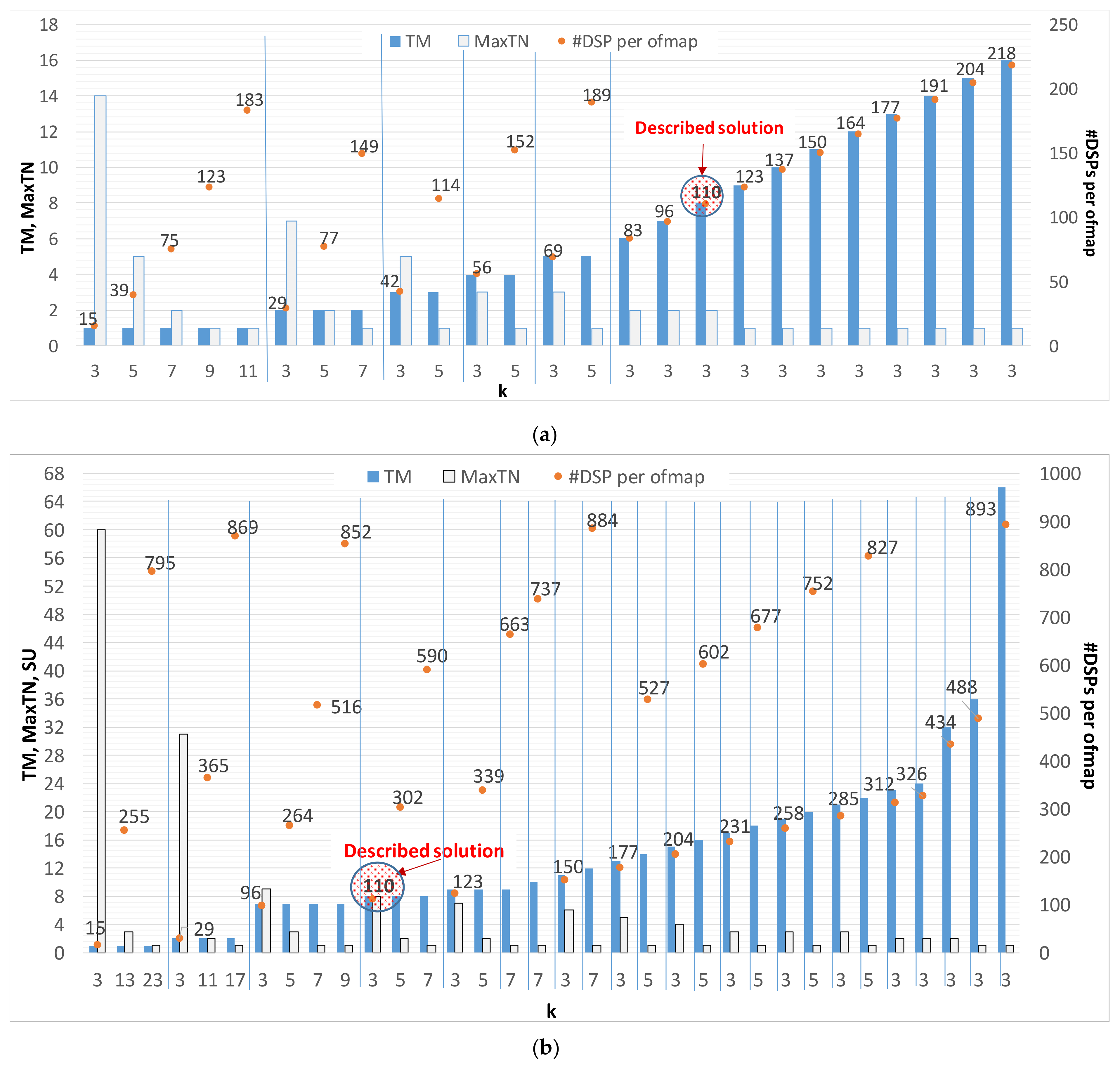
As a further characterization of the proposed architecture, a design space exploration is presented to analyze resources requirements versus the computational parallelism (i.e., TM and TN) and the convolution kernel size (K). Figure 9a,b plot the results related to the XC7Z020 and XC7Z045 device, respectively. In order to become familiarized with information contained in the diagrams, let’s examine the leftmost portion of Figure 9a. There, several kernel sizes (K = 3, 5, 7, 9, 11) are considered, with TM = 1. Obviously, the wider the convolution kernel, the higher the number of DSPs used by a single PE. This means that the maximum number of ofmaps computed in parallel (MaxTN) by the CE is limited by the amount of available resources. Referring to the cases in which TM = 1, the number of DSPs used by each PE ranges from 15 to 183 for K varying from 3 to 11, respectively, while up to 14 ofmaps can be processed in parallel. Of course, the larger XC7Z045 device allows convolution kernels wider than 11 to be also used in the PE. Figure 9 clearly shows that generally a theoretical speed-up (SU = TM × TN) with respect to the case in which TM = TN = 1 can be obtained with various configurations. As an example, SU = 16 can be achieved for different values of TM and TN (e.g., TM = 8 and TN = 2, TM = 16 and TN = 1, and so on). Each of the implementable solutions offers its own benefit, depending on the actually exploitable parallelism, which is bounded by the limited capability of DMAs and HP ports. Indeed, when AXI transactions wider than 64-bit are required, they are performed over more than one clock cycle. In such cases, the actual speed-up is consequently reduced with respect to the above-mentioned theoretical level.
Referring to Figure 9b, all configurations with either TM or TN above 16 are influenced by such an effect. As an example, the configuration (TM = 17, TN = 3, K = 3) shows an actual speed-up of 24 over the theoretical SU = TM × TN = 51. Due to this limitation, several possible configurations that can be accommodated in the XC7Z045 device do not actually benefit from the increased parallelism. However, they can be efficiently exploited in high performance UltrascaleTM devices. In such cases, frame rates up to 55 fps can be achieved for the inference of VGG-16.
Finally, to demonstrate that the proposed embedded design can also be adapted to accelerate CNN models characterized by non-uniform kernel sizes across layers, we implemented the VGG-S model [8], since it uses cascaded layers with 7 × 7, 5 × 5 and 3 × 3 convolutional kernels. In such cases, the number of convolution windows prepared by the buffer is a function of the current CONV layer and its kernel size. This leads to an effective ifmaps parallelism level that scales as the kernel size K increases. The proposed accelerator processes the input stream as above detailed. Due to the reduced number of convolution windows, some of the DSPs available within the DMAC blocks are not used as MAC operators. Indeed, they are exploited to perform auxiliary accumulations, thus reducing the overall latency. The PS, dispatching the required information to the FSM, manages the runtime reconfiguration of the above modules. Through the performed tests, we observed that the XC7Z020 and XC7Z045 implementations complete all the convolutional layers within just ~44.6 ms and ~10 ms respectively.
5. Conclusions
In this paper, an efficient heterogeneous SoC design was proposed to accelerate the inference of reduced precision CNNs. The novel architecture exploits an effective hardware/software partitioning, in which the computational-intensive CONV layers are performed by a specialized hardware architecture, whereas the memory-intensive FC layers are executed by a software routine running on the processor. Both the hardware and software computations support the efficient SIMD paradigm for processing multiple data in parallel. In the custom hardware design, the number of executed MACs is doubled by mapping two independent products A × C and B × C within a single DSP slice, thus allowing the parallel computation of adjacent convolutional windows. The software design was developed to enable the NEON multimedia engine for high-performance vector-based elaborations. Two implementations of the proposed embedded system were characterized for large-scale CNNs on the Xilinx Zynq-7000 SoC family. Such prototypes exceed the capabilities of state-of-the-art implementations realized on the same embedded platforms, reaching a power efficiency significantly higher than competitive prior works and, therefore, becoming good candidates for the realization of power-constrained high-performance intelligent systems. The proposed strategy allows the accelerator to be easily configured for various kernels sizes and parallelism levels. As an example, when it is used for accelerating the large-scale VGG-16 model, our design reaches a computational time as low as ~376 ms and ~84 ms on the XC7Z020 and XC7Z045 devices, respectively. Of course, simplified CNN models, such as the VGG-S, allow further higher-speed performances. In such cases, the proposed architecture exhibits a frame rate of up to 100 fps.
Author Contributions
Conceptualization, F.S., S.P., F.F. and P.C.; formal analysis, F.S., S.P., F.F. and P.C.; investigation, F.S., S.P., F.F. and P.C.; validation, F.S., S.P., F.F. and P.C.; writing—review and editing, F.S., S.P., F.F. and P.C. All authors have read and agreed to the published version of the manuscript.
Funding
This research received no external funding.
Conflicts of Interest
The authors declare no conflict of interest.
References
- Sze, V.; Chen, H.; Yang, T.J.; Emer, J. Efficient Processing of Deep Neural Networks: A Tutorial and Survey. Proc. IEEE 2017, 105, 2295–2329. [Google Scholar] [CrossRef] [Green Version]
- Ranjan, R.; Patel, V.M.; Chellappa, R. HyperFace: A Deep Multi-task Learning Framework for Face Detection, Landmark Localization, Pose Estimation, and Gender Recognition. IEEE Trans. Pattern Anal. Mach. Learn. 2019, 41, 121–135. [Google Scholar] [CrossRef] [PubMed] [Green Version]
- Jaderberg, M.; Simonyan, K.; Vedaldi, A.; Zisserman, A. Reading Text in the Wild with Convolutional Neural Networks. Int. J. Comput. Vis. 2016, 116, 1–20. [Google Scholar] [CrossRef] [Green Version]
- Zhang, Y.; Chan, W.; Jaitly, N. Very deep convolutional networks for end-to-end speech recognition. In Proceedings of the 2017 IEEE International Conference on Acoustics, Speech and Signal Processing (ICASSP), New Orleans, LA, USA, 5–9 March 2017. [Google Scholar]
- Wang, X.; Zhang, W.; Wu, X.; Xiao, L.; Qian, Y.; Fang, Z. Real-time vehicle type classification with deep convolutional neural networks. J. Real Time Image Process. 2019, 16, 5–14. [Google Scholar] [CrossRef]
- Du, L.; Du, Y.; Li, Y.; Su, J.; Kuan, Y.; Liu, C.; Chang, M.F. A Reconfigurable Streaming Deep Convolutional Neural Network Accelerator for Internet of Things. IEEE Trans. Circ. Syst. 2018, 65, 198–208. [Google Scholar] [CrossRef] [Green Version]
- Simonyan, K.; Zisserman, A. Very Deep Convolutional Networks for Large-Scale Image Recognition. 2014. Available online: https://arxiv.org/abs/1409.1556 (accessed on 14 November 2019).
- Chatfield, K.; Simonyan, K.; Vedaldi, A.; Zisserman, A. Return of the Devil in the Details: Delving Deep into Convolutional Nets. Available online: https://arxiv.org/pdf/1405.3531.pdf (accessed on 14 November 2019).
- He, K.; Zhang, X.; Ren, S.; Sun, J. Deep Residual Learning for Image Recognition. In Proceedings of the IEEE Conference on Computer Vision and Pattern Recognition (CVPR), Las Vegas, NV, USA, 27–30 June 2016; pp. 770–779. [Google Scholar]
- Szegedy, C.; Liu, W.; Jia, Y.; Sermanet, P.; Reed, S.; Anguelov, D.; Erhan, D.; Vanhoucke, V.; Rabinovich, A. Going Deeper with Convolutions. In Proceedings of the IEEE Conference on Computer Vision and Pattern Recognition (CVPR), Boston, MA, USA, 7–12 June 2015; pp. 1–9. [Google Scholar]
- Judd, P.; Albericio, J.; Hetherington, T.; Aamodt, T.; Jerger, N.E.; Urtasun, R.; Moshovos, A. Proteus: Exploiting precision variability in deep neural networks. Parallel Comput. 2018, 73, 40–51. [Google Scholar] [CrossRef]
- Gysel, P.; Motamedi, M.; Ghiasi, S. Hardware-Oriented Approximation of Convolutional Neural Networks. 2016. Available online: https://arxiv.org/abs/1604.03168 (accessed on 14 November 2019).
- Wu, S.; Li, G.; Chen, F.; Shi, L. Training and Inference with Integers in Deep Neural Networks. 2018. Available online: https://arxiv.org/abs/1802.04680 (accessed on 14 November 2019).
- Rodriguez, A.; Segal, E.; Meiri, E.; Fomenko, E.; Kim, Y.J.; Shen, H.; Ziv, B. Lower Numerical Precision Deep Learning Inference and Training. Available online: https://software.intel.com/en-us/articles/lower-numerical-precision-deep-learning-inference-and-training (accessed on 14 November 2019).
- Horowitz, M. Computing’s energy problem (and what we can do about it). In Proceedings of the 2014 IEEE International Solid-State Circuits Conference, San Francisco, CA, USA, 9–13 February 2014; pp. 10–14. [Google Scholar]
- Lian, X.; Liu, Z.; Song, Z.; Dai, J.; Zhou, W.; Ji, X. High-Performance FPGA-Based CNN Accelerator with Block-Floating-Point Arithmetic. IEEE Trans. VLSI Syst. 2019, 27, 1874–1885. [Google Scholar] [CrossRef]
- Chen, Q.; Fu, X.; Song, W.; Cheng, K.; Lu, Z.; Zhang, C.; Li, L. An Efficient Streaming Accelerator for Low Bit-Width Convolutional Neural Networks. Electronics 2019, 8, 371. [Google Scholar] [CrossRef] [Green Version]
- Zhang, M.; Li, L.; Wang, H.; Liu, Y.; Qin, H.; Zhao, W. Optimized Compression for Implementing Convolutional Neural Networks on FPGA. Electronics 2019, 8, 295. [Google Scholar] [CrossRef] [Green Version]
- Tlelo-Cuautle, E.; Rangel-Magdaleno, J.; Gerardo de la Fraga, L. Engineering Applications of FPGAs; Springer Book: Basel, Switzerland, 2016. [Google Scholar]
- Pano-Azucena, A.D.; Tlelo-Cuautle, E.; Tan, S.X.D.; Ovilla-Martinez, B.; Gerardo de la Fraga, L. FPGA-Based Implementation of a Multilayer Perceptron Suitable for Chaotic Time Series Prediction. Technologies 2018, 6, 90. [Google Scholar] [CrossRef] [Green Version]
- Zynq-7000 SoC Technical Reference Manual, UG585 (v1.12.2). 1 July 2018. Available online: www.xilinx.com (accessed on 14 November 2019).
- Zynq Ultrascale+ Device Technical Reference Manual, UG1085 (v. 1.8). 3 August 2018. Available online: www.xilinx.com (accessed on 14 November 2019).
- Stratix 10 GX/SX Device Overview. Available online: www.intel.com (accessed on 14 November 2019).
- Arria 5/10 SoC FPGAs. Available online: www.intel.com (accessed on 14 November 2019).
- HajiRassouliha, A.; Taberner, A.J.; Nash, M.P.; Nielsen, P.M.F. Suitability of recent hardware accelerators (DSPs, FPGAs, and GPUs) for computer vision and image processing algorithms. Signal Process. Image Commun. 2018, 68, 101–119. [Google Scholar] [CrossRef]
- Venieris, S.I.; Bouganis, C.S. fpgaConvNet: Mapping Regular and Irregular Convolutional Neural Networks on FPGAs. IEEE Trans. Neural Netw. Learn. Syst. 2018, 30, 326–342. [Google Scholar] [CrossRef] [PubMed] [Green Version]
- Chen, X.; Yu, Z. A Flexible and Energy-Efficient Convolutional Neural Network Acceleration with Dedicated ISA and Accelerator. IEEE Trans. VLSI Syst. 2018, 26, 1408–1412. [Google Scholar] [CrossRef]
- Ma, Y.; Cao, Y.; Vrudhula, S.; Seo, J. Optimizing the Convolution Operation to Accelerate Deep Neural Networks on FPGA. IEEE Trans. VLSI Syst. 2018, 26, 1354–1367. [Google Scholar] [CrossRef]
- Aimar, A.; Mostafa, H.; Calabrese, E.; Rios-Navarro, A.; Tapiador-Moralese, R.; Lungu, I.A.; Milde, M.B.; Corradi, F.; Linares-Barranco, A.; Liu, S.C.; et al. NullHop: A Flexible Convolutional Neural Network Accelerator Based on Sparse Representations of Feature Maps. IEEE Trans. Neural Netw. Learn. Syst. 2018, 30, 644–656. [Google Scholar] [CrossRef] [PubMed] [Green Version]
- Guo, K.; Sui, L.; Qiu, J.; Yu, J.; Wang, J.; Yao, S.; Han, S.; Wang, Y.; Yang, H. Angel-Eye: A Complete Design Flow for Mapping CNN onto Embedded FPGA. IEEE Trans. CAD Integr. Circuits Syst. 2018, 37, 35–47. [Google Scholar] [CrossRef]
- Li, G.; Li, F.; Zhao, T.; Cheng, J. Block Convolution: Towards Memory-Efficient Inference of Large-Scale CNNs on FPGA. In Proceedings of the 2018 Design, Automation & Test in Europe Conference & Exhibition, Dresden, Germany, 19–23 March 2018; pp. 1163–1166. [Google Scholar]
- Jin, X.; Xu, C.; Feng, J.; Wei, Y.; Xiong, J.; Yan, S. Deep learning with S-shaped rectified linear activation units. In Proceedings of the Thirtieth AAAI Conference on Artificial Intelligence, Phoenix, AZ, USA, 12–17 February 2016. [Google Scholar]
- Cong, J.; Xiao, B. Minimizing computation in convolutional neural networks. In Proceedings of the 24th International Conference on Artificial Neural Networks, Hamburg, Germany, 15–19 September 2014; pp. 281–290. [Google Scholar]
- Meloni, P.; Capotondi, A.; Deriu, G.; Brian, M.; Conti, F.; Rossi, D.; Raffo, L.; Benini, L. NEURAghe: Exploiting CPU-FPGA Synergies for Efficient and Flexible CNN Inference Acceleration on Zynq SoCs. ACM Trans. Reconfig. Technol. Syst. 2018, 11, 18. [Google Scholar] [CrossRef] [Green Version]
- Spagnolo, F.; Perri, S.; Frustaci, F.; Corsonello, P. Designing Fast Convolution Engines for Deep Learning Applications. In Proceedings of the 25th IEEE International Conference on Electronics, Circuits and Systems, Bordeaux, France, 9–12 December 2018. [Google Scholar]
- Kouris, A.; Venieris, S.I.; Bouganis, C.S. Cascade^CNN: Pushing the Performance Limits of Quantisation in Convolutional Neural Networks. In Proceedings of the 28th International Conference on Field Programmable Logic and Applications, Dublin, Ireland, 27–31 August 2018. [Google Scholar]
- Lee, S.; Kim, D.; Nguyen, D.; Lee, J. Double MAC on a DSP: Boosting the Performance of Convolutional Neural Networks on FPGAs. IEEE Trans. CAD Integr. Circuits Syst. 2018, 38, 888–897. [Google Scholar] [CrossRef]
- AMBA AXI4, AXI4-Lite, and AXI4-Stream Protocol Assertion User Guide. Available online: www.infocenter.arm.com (accessed on 14 November 2019).
- Cortex-A9 NEON Media Processing Engine Technical Reference Manual, rev. r3p0. Available online: www.infocenter.arm.com (accessed on 14 November 2019).
- Xilinx Zynq-7000 External Memory Interfaces. Available online: https://www.xilinx.com/products/technology/memory.html#externalMemory (accessed on 14 November 2019).
Figure 1.
Computations performed by: (a) a convolutional layer; (b) a fully connected layer.

Figure 2.
Top-level architecture of the proposed accelerator for CNNs.

Figure 3.
Architecture of the reconfigurable SIMD Buffer.

Figure 4.
Dispatching two adjacent windows by the proposed buffer architecture: (a) example on a 4 × 8 input; (b) the strategy used to recouple input data; (c) data provided by the registers depending on nr.
Figure 4.
Dispatching two adjacent windows by the proposed buffer architecture: (a) example on a 4 × 8 input; (b) the strategy used to recouple input data; (c) data provided by the registers depending on nr.

Figure 5.
SIMD multiplication with a common operand C and no guard-bit.

Figure 6.
Architecture of the proposed SIMD CE.

Figure 7.
The pseudo-code used to accelerate FC and softmax layers.

Figure 8.
The proposed embedded system on Zynq-7000 devices.

Figure 9.
Analysis of the computational capabilities achievable within: (a) the XC7Z020 device; (b) the XC7Z045 device.
Figure 9.
Analysis of the computational capabilities achievable within: (a) the XC7Z020 device; (b) the XC7Z045 device.


Table 1.
Comparison results.
| Design (Device) | Freq. [MHz] | Gops | DSPs | Other Resources | DE (Gops/ DSPs) | CONVs Time [ms] | FCs+ Softmax Time [ms] | PEff (Gops/W) | |||
|---|---|---|---|---|---|---|---|---|---|---|---|
| LUTs | FFs | BRAMs [Mb] | |||||||||
| New | ES 1 (XC7Z020 [18]) | 150 | 95.5 | 220 (100%) | 13,455 (25.3%) | 19,129 (18%) | 3.44 (70%) | 0.434 | 376.3 | 48 | 38.5 |
| [30] | SA 2 (XC7Z020 [18]) | 150 | 84.3 | 190 (86.3%) | 29,867 (56%) | 35,489 (33%) | 3 (61%) | 0.443 | 364 | NP 4 | 24.1 |
| [26] | ES (XC7Z020 [18]) | 125 | 48.53 | 220 (100%) | NA 3 | NA | NA | 0.22 | 633 | NP | 27.7 |
| New | ES (XC7Z045 [18]) | 167 | 425.32 | 880 (97.8%) | 30,161 (13.8%) | 47,832 (10.9%) | 12.9 (67.5%) | 0.48 | 84.5 | 48 | 135 |
| [27] | SA (XC7Z045 [18]) | 150 | 36.8 | 197 (21.8%) | 18,578 (8.5%) | 8049 (1.84%) | 0.773 (4%) | 0.186 | 1639.3 | NP | 79.7 |
| [30] | SA (XC7Z045 [18]) | 214 | 137 | 780 (86.6%) | 182,616 (84%) | 127,653 (29%) | 17.08 (87%) | 0.175 | 224.6 | NP | 14.2 |
| [26] | ES (XC7Z045 [18]) | 125 | 155.81 | 855 (95%) | NA | NA | NA | 0.182 | 249.5 | NP | 38.8 |
| [31] | SA (XC7Z045 [18]) | 150 | 374.98 | 900 (100%) | 113,672 (52%) | 240,640 (55%) | 19.16 (100%) | 0.416 | 82.03 | NP | NA |
| [34] | ES (XC7Z045 [18]) | 140 | 169 | 864 (96%) | 88,154 (35.1%) | 61,250 (14.1%) | 11.25 (58.7%) | 0.195 | 181.8 | 72.6 | 16.9 |
| [29] | ES (XC7Z100 [18]) | 60 | 17.2 | 128 (6.3%) | 229,000 (83%) | 107,000 (19%) | 13.6 (51.1%) | 0.134 | 2269 * | *included | 27.4 |
| [28] | ES (GX1150 [21]) | 200 | 715.9 | 1518 (100%) | 141,312 (32%) | NA | 43.6 (82%) | 0.47 | 43.2 * | *included | NA |
1 Embedded system; 2 Standalone accelerator; 3 Not available; 4 Not performed.
© 2019 by the authors. Licensee MDPI, Basel, Switzerland. This article is an open access article distributed under the terms and conditions of the Creative Commons Attribution (CC BY) license (http://creativecommons.org/licenses/by/4.0/).
Share and Cite
MDPI and ACS Style
Spagnolo, F.; Perri, S.; Frustaci, F.; Corsonello, P. Energy-Efficient Architecture for CNNs Inference on Heterogeneous FPGA. J. Low Power Electron. Appl. 2020, 10, 1. https://0-doi-org.brum.beds.ac.uk/10.3390/jlpea10010001
AMA Style
Spagnolo F, Perri S, Frustaci F, Corsonello P. Energy-Efficient Architecture for CNNs Inference on Heterogeneous FPGA. Journal of Low Power Electronics and Applications. 2020; 10(1):1. https://0-doi-org.brum.beds.ac.uk/10.3390/jlpea10010001
Chicago/Turabian StyleSpagnolo, Fanny, Stefania Perri, Fabio Frustaci, and Pasquale Corsonello. 2020. "Energy-Efficient Architecture for CNNs Inference on Heterogeneous FPGA" Journal of Low Power Electronics and Applications 10, no. 1: 1. https://0-doi-org.brum.beds.ac.uk/10.3390/jlpea10010001
Note that from the first issue of 2016, this journal uses article numbers instead of page numbers. See further details here.