High-Efficiency Switched-Capacitor DC-DC Converter with Three Decades of Load Current Range Using Adaptively-Biased PFM


Abstract
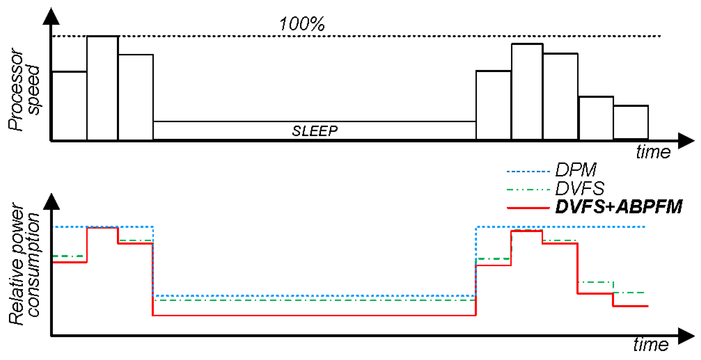
:1. Introduction
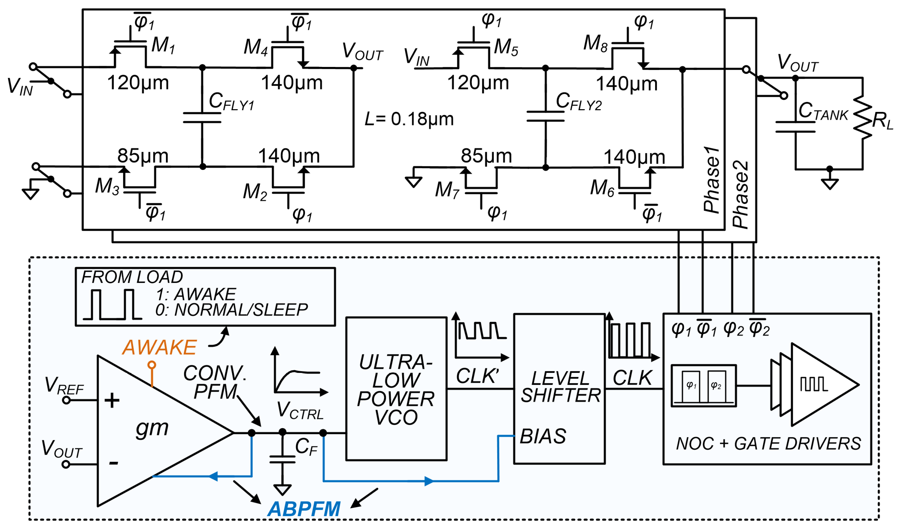
2. SC DC-DC Converter Design and Controller
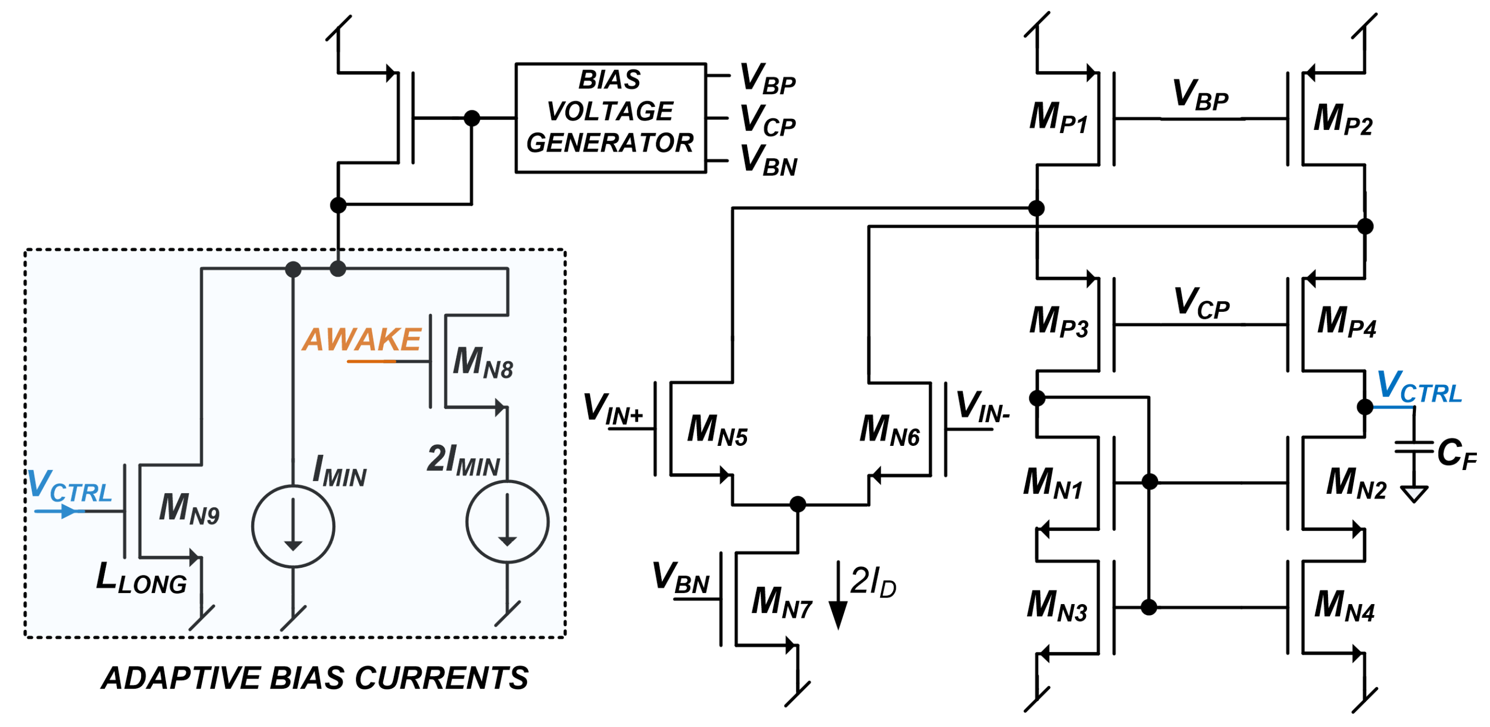
2.1. Adaptively-Biased Folded-Cascode Amplifier
2.2. Ultra-Low Power VCO and Level Shifter
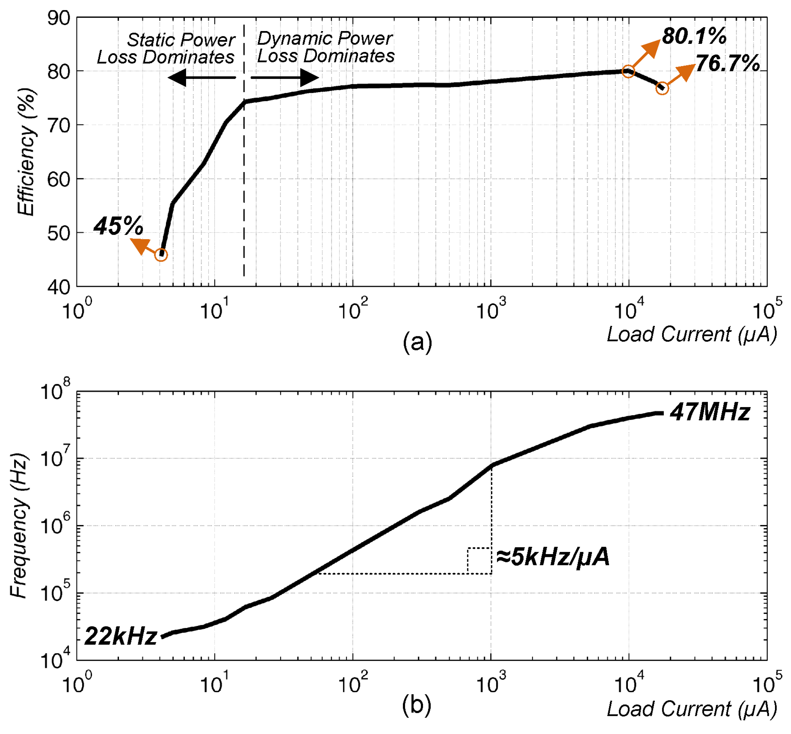
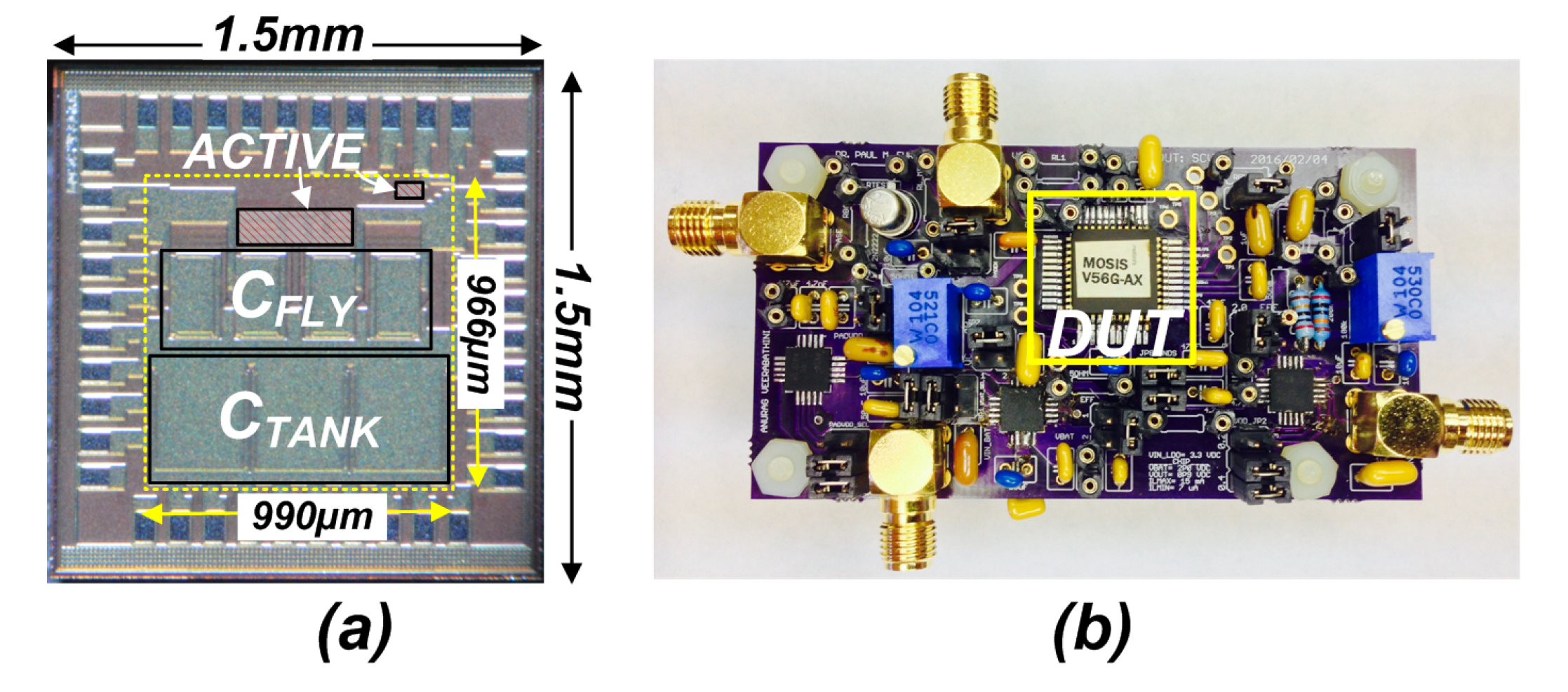
3. Implementation and Measurement Results
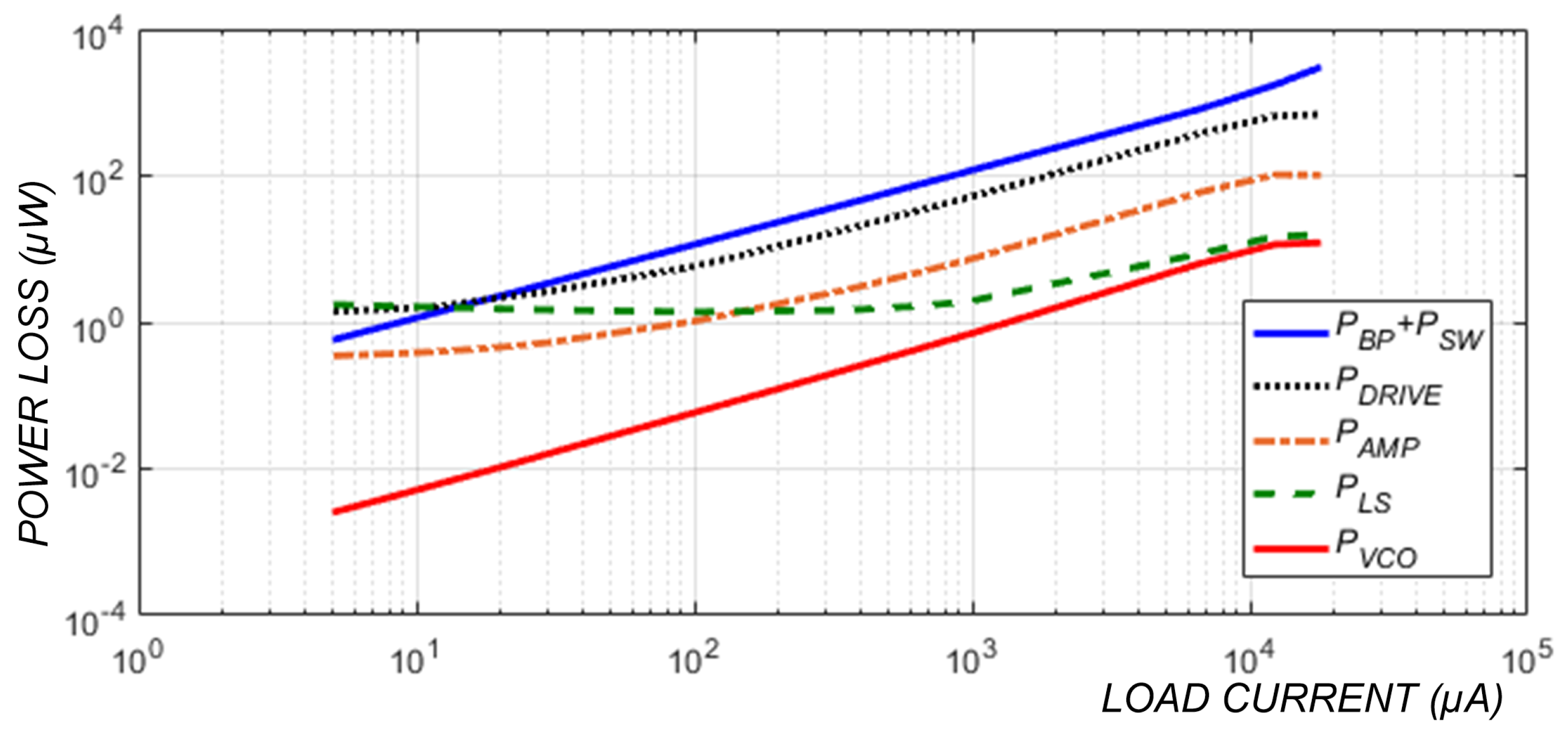
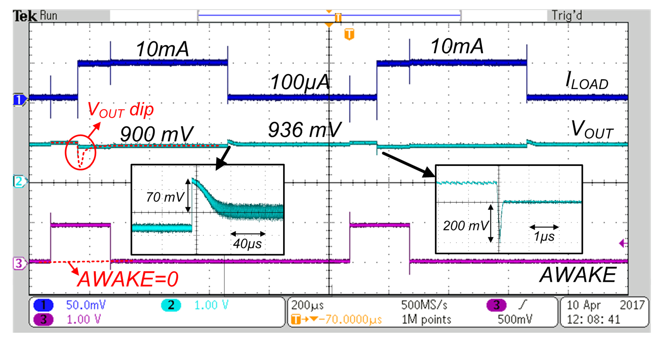
3.1. Hardware Measurements
3.2. Comparison
4. Conclusions
Author Contributions
Funding
Acknowledgments
Conflicts of Interest
References
- Wang, A.; Lin, T.; Ouyang, S.; Huang, W.; Wang, J.; Chang, S.; Chen, S.; Hu, C.; Tai, J.C.; Tan, K.; et al. 10.3 Heterogeneous Multi-processing quad-core CPU and dual-GPU Design for optimal performance, power, and thermal tradeoffs in a 28 nm mobile application processor. In Proceedings of the 2014 IEEE International Solid-State Circuits Conference Digest of Technical Papers (ISSCC), San Francisco, CA, USA, 9–13 February 2014; pp. 180–181. [Google Scholar] [CrossRef]
- Jiang, J.; Lu, Y.; Ki, W.H.; Seng-Pan, U.; Martins, R.P. A dual-symmetrical-output switched-capacitor converter with dynamic power cells and minimized cross regulation for application processors in 28 nm CMOS. In Proceedings of the 2017 IEEE International Solid-State Circuits Conference (ISSCC), San Francisco, CA, USA, 5–9 February 2017; pp. 344–345. [Google Scholar] [CrossRef]
- Jevtić, R.; Le, H.P.; Blagojević, M.; Bailey, S.; Asanović, K.; Alon, E.; Nikolić, B. Per-Core DVFS With Switched-Capacitor Converters for Energy Efficiency in Manycore Processors. IEEE Trans. Very Large Scale Integr. (VLSI) Syst. 2015, 23, 723–730. [Google Scholar] [CrossRef]
- Kilani, D.; Alhawari, M.; Mohammad, B.; Saleh, H.; Ismail, M. An Efficient Switched-Capacitor DC-DC Buck Converter for Self-Powered Wearable Electronics. IEEE Trans. Circuits Syst. I Reg. Pap. 2016, 63, 1557–1566. [Google Scholar] [CrossRef]
- Furth, P.M.; Veerabathini, A.; Saifullah, Z.M.; Rivera, D.T.; Elkanishy, A.; Badawy, A.A.; Michael, C.P. Supervisory Circuits for Low-Frequency Monitoring of a Communication SoC. In Proceedings of the 2019 IEEE 62nd International Midwest Symposium on Circuits and Systems (MWSCAS), Dallas, TX, USA, 4–7 August 2019; pp. 17–20. [Google Scholar] [CrossRef]
- Krihely, N.; Ben-Yaakov, S.; Fish, A. Efficiency Optimization of a Step-Down Switched Capacitor Converter for Subthreshold. IEEE Trans. Very Large Scale Integr. (VLSI) Syst. 2013, 21, 2353–2357. [Google Scholar] [CrossRef]
- Andersen, T.M.; Krismer, F.; Kolar, J.W.; Toifl, T.; Menolfi, C.; Kull, L.; Morf, T.; Kossel, M.; Brändli, M.; Buchmann, P.; et al. A 4.6W/mm2 power density 86% efficiency on-chip switched capacitor DC-DC converter in 32 nm SOI CMOS. In Proceedings of the IEEE Applied Power Electronics Conference and Exposition (APEC), Long Beach, CA, USA, 17–21 March 2013; pp. 692–699. [Google Scholar] [CrossRef]
- Butzen, N.; Steyaert, M.S.J. Scalable Parasitic Charge Redistribution: Design of High-Efficiency Fully Integrated Switched-Capacitor DC-DC Converters. IEEE J. Solid-State Circuits 2016, 51, 2843–2853. [Google Scholar] [CrossRef]
- Ma, D.; Bondade, R. Reconfigurable Switched-Capacitor Power Converters— Principles and Designs for Self-Powered Microsystems; Springer: Berlin/Heidelberg, Germany, 2013. [Google Scholar]
- Veerabathini, A.; Furth, P.M. A Low Output Voltage Ripple Fully-Integrated Switched-Capacitor DC-DC Converter. In Proceedings of the 2019 IEEE 62nd International Midwest Symposium on Circuits and Systems (MWSCAS), Dallas, TX, USA, 4–7 August 2019; pp. 937–940. [Google Scholar] [CrossRef]
- Patounakis, G.; Li, Y.W.; Shepard, K.L. A fully integrated on-chip DC-DC conversion and power management system. IEEE J. Solid-State Circuits 2004, 39, 443–451. [Google Scholar] [CrossRef]
- Baker, R. CMOS: Circuit Design, Layout, and Simulation, 2nd ed.; Wiley: Hoboken, NJ, USA, 2011; pp. 796–808. [Google Scholar]
- Mattingly, D. Designing Stable Compensation Networks for Single Phase Voltage Mode Buck Regulators. Available online: https://e2echina.ti.com/cfs-file/__key/telligent-evolution-components-attachments/00-24-01-00-00-03-73-41/Compensation-Network.pdf (accessed on 19 April 2019).
- Wen, L.; Cheng, X.; Tian, S.; Wen, H.; Zeng, X. Subthreshold Level Shifter With Self-Controlled Current Limiter by Detecting Output Error. IEEE Trans. Circuits Syst. II Exp. Briefs 2016, 63, 346–350. [Google Scholar] [CrossRef]
- Lanuzza, M.; Crupi, F.; Rao, S.; Rose, R.D.; Strangio, S.; Iannaccone, G. An Ultralow-Voltage Energy-Efficient Level Shifter. IEEE Trans. Circuits Syst. II Exp. Briefs 2017, 64, 61–65. [Google Scholar] [CrossRef]
- Abdelmoaty, A.; Al-Shyoukh, M.; Fayed, A. A high-voltage level shifter with sub-nano-second propagation delay for switching power converters. In Proceedings of the 2016 IEEE Applied Power Electronics Conference and Exposition (APEC), Long Beach, CA, USA, 20–24 March 2016; pp. 2437–2440. [Google Scholar] [CrossRef]
- Veerabathini, A.; Eshappa, N.B.; Furth, P.M. Low-power pulse width modulation (PWM) for high-frequency DC–DC converters. Electron. Lett. 2018, 54, 585–587. [Google Scholar] [CrossRef]
- Andersen, T.M.; Krismer, F.; Kolar, J.W.; Toifl, T.; Menolfi, C.; Kull, L.; Morf, T.; Kossel, M.; Brändli, M.; Francese, P.A. Modeling and Pareto Optimization of On-Chip Switched Capacitor Converters. IEEE Trans. Power Electron. 2017, 32, 363–377. [Google Scholar] [CrossRef]
- Le, H.P.; Sanders, S.R.; Alon, E. Design Techniques for Fully Integrated Switched-Capacitor DC-DC Converters. IEEE J. Solid-State Circuits 2011, 46, 2120–2131. [Google Scholar] [CrossRef]
- Evzelman, M.; Ben-Yaakov, S. Average-Current-Based Conduction Losses Model of Switched Capacitor Converters. IEEE Trans. Power Electron. 2013, 28, 3341–3352. [Google Scholar] [CrossRef]
- Lutz, D.; Renz, P.; Wicht, B. A 10 mW fully integrated 2-to-13V input buck-boost SC converter with 81.5% peak efficiency. In Proceedings of the 2016 IEEE International Solid-State Circuits Conference (ISSCC), San Francisco, CA, USA, 31 January–4 February 2016; pp. 224–225. [Google Scholar] [CrossRef]
- Hua, Z.; Lee, H. Adaptive-on-time control technique for output ripple reduction and light-load efficiency enhancement in low-power switched-capacitor DC-DC regulators. In Proceedings of the 2015 IEEE Applied Power Electronics Conference and Exposition (APEC), Charlotte, NC, USA, 15–19 March 2015; pp. 1930–1933. [Google Scholar] [CrossRef]


| Parameter | [8] | [18] | [21] | [22] | This Work |
|---|---|---|---|---|---|
| Process | 40 nm | 32 nm SOI | 0.35 m | 0.35 m | 0.18 m |
| metal-oxide-metal | deep trench | MIM | Off-chip | MIM | |
| NO | Off-chip | - | Off-chip | dual MIM | |
| Conversion Ratio | 1/2 | 1/2 | 5/13 -5/2 | 2/1, 3/1 | 1/2 |
| Control Scheme | Hysteretic | PFM | PFM | Adaptive-on-time | ABPFM |
| (V) | 1.85–2.07 | 1.8 | 2–13 | 1.1–1.8 | 2.0 |
| (V) | 0.9 | 0.836 | 5 | 2, 3 | 0.9 |
| (A) | 4.25 m | 19.1 m † | 4 m | 12 m | 17.8 m |
| (A) | 167 † | 5.2 m † | 500 † | 500 | 12 |
| (%) | 94.6 | 86 | 81.5 | 89.5 | 80 |
| (%) | 60 † | 80 | 60 † | 75 | 70 |
| (F) | 10 n | 690 p | - | 4.7 | 515 p |
| (F) | 0 | 33 n | 3.64 n * | 1 | 1.2 n |
| Area (mm) | 2.4 | 0.00344 | 6.8 | 6.9 | 0.96 |
| (W/mm) | 1.6 m | 4.6 | 3.0 m | 5.2 m | 16.8 m |
| 1.06 | 0.47 | 0.63 | 1.13 | 2.37 |
© 2020 by the authors. Licensee MDPI, Basel, Switzerland. This article is an open access article distributed under the terms and conditions of the Creative Commons Attribution (CC BY) license (http://creativecommons.org/licenses/by/4.0/).
Share and Cite
Veerabathini, A.; Furth, P.M. High-Efficiency Switched-Capacitor DC-DC Converter with Three Decades of Load Current Range Using Adaptively-Biased PFM. J. Low Power Electron. Appl. 2020, 10, 5. https://0-doi-org.brum.beds.ac.uk/10.3390/jlpea10010005
Veerabathini A, Furth PM. High-Efficiency Switched-Capacitor DC-DC Converter with Three Decades of Load Current Range Using Adaptively-Biased PFM. Journal of Low Power Electronics and Applications. 2020; 10(1):5. https://0-doi-org.brum.beds.ac.uk/10.3390/jlpea10010005
Chicago/Turabian StyleVeerabathini, Anurag, and Paul M. Furth. 2020. "High-Efficiency Switched-Capacitor DC-DC Converter with Three Decades of Load Current Range Using Adaptively-Biased PFM" Journal of Low Power Electronics and Applications 10, no. 1: 5. https://0-doi-org.brum.beds.ac.uk/10.3390/jlpea10010005