Article

Electronic Tuning Square-Wave Generators with Improved Linearity Using Operational Transresistance Amplifier

by
Pittala Chandra Shaker
1 and
Avireni Srinivasulu
2,*
1
Department of Electronics and Communication Engineering, MLR Institute of Technology, Hyderabad 500043, India
2
Department of Electronics and Communication Engineering, JECRC University, Jaipur 303905, India
*
Author to whom correspondence should be addressed.
J. Low Power Electron. Appl. 2020, 10(2), 12; https://0-doi-org.brum.beds.ac.uk/10.3390/jlpea10020012
Submission received: 25 March 2020 / Revised: 10 April 2020 / Accepted: 12 April 2020 / Published: 14 April 2020

Abstract

:
Two new electronic tuning current-mode square-wave generators are introduced in the ensuing paper. In the first proposed square-wave generator circuit, one Operational Trans-resistance Amplifier (OTRA) and two passive components are involved, along with two NMOS depletion mode transistors. This circuit generates a square-wave with almost equal and fixed duty cycles. The second proposed circuit is able to control both on-duty and off-duty cycles independently with the help of two passive components, two NMOS depletion mode transistors, and two diodes connected to the circuit. The frequency of the proposed circuits can be adjusted with the passive components connected to the circuit. Moreover, electronic tuning can also be achieved with the proposed circuits. The measured results that are included in the paper show the linear variation of a time period as compared with existing OTRA based square waveform generator. The performance of the proposed circuits is examined while using SPICE models. These circuits are built on a laboratory breadboard using commercially available Current Feedback Operational Amplifier (AD844 AN) and passive components are connected externally and tested for square waveform generation. The obtained results demonstrate good agreement with the theoretical values.

1. Introduction

The square-wave generator is widely operated in many electronic fields, such as digital, instrumentation, and communication systems. Conventionally, Operational Amplifier (Op-Amp) is used to generate square waveform along with some passive components. These voltage-mode (Op-Amp) circuits pose some drawbacks, such as complex internal circuitry, lower slew rate, constant gain bandwidth product, and more passive components are, however, required to generate the waveforms [1].
Recently, an alternative approach, called current-mode technology, has attracted considerable attention for analog circuit designers, due to its advantage over voltage-mode devices, like high performance, high linearity, wide dynamic range, low power consumption, simple circuitry, and versatility over voltage-mode devices [2]. Several waveform generators have been proposed using current-mode devices; these waveform generator circuits offer several advantages over voltage-mode waveform generators. The circuits that are given in [3,4,5,6,7,8,9,10,11,12,13,14] are designed with Voltage Differencing Buffered/Inverted Amplifier (VDIBA), Multiple Output Current Through Transconductance Amplifiers (MO-CTTA), Controlled Gain Current and Differential Voltage Amplifier (CG-CDVA), Differential Voltage Current Conveyors (DVCC), and Operational Transconductance Amplifier (OTA). These square-wave generators require external voltage or current biasing to produce the square waveform. Current Feedback Operational Amplifier (CFOA) based waveform generator was introduced in [15]. However, this waveform generator requires more passive components and two active components. A single CFOA based waveform generator was proposed in [16]. The configuration of the circuit is simple with a few passive components. However, the oscillation frequencies are limited to few kHz. Second generation Current Conveyor (CCII+) based waveform generators were proposed in the literature [17,18,19,20,21]. These waveform generators provide some advantages, like higher slew rate and wider bandwidth. However, some of these waveform generators require more than one active device and more passive components. Square-wave generators with single CCII+ were proposed in [20]. These waveform generators have the advantage of less power consumption. However, the oscillation frequencies of these circuits are limited to only few kHz. The square-wave generator using three operational transconductance amplifier (OTA) and three passive components was proposed in [22]. The advantage of this waveform generator would be that it can control the amplitude and frequency independently by changing the resistance or changing the biasing current. However, this waveform generator consumes more power and the use of three OTAs requires more chip area. Table 1 shows the comparison of active devices.
Recently, an active current-mode device, called an operational transresistance amplifier (OTRA), has come to limelight with the introduction of several high performances CMOS OTRA realizations. Several waveform generators using an operational transresistance amplifier (OTRA) were reported earlier in the literature [23,24,25,26,27,28,29,30,31,32,33,34,35,36,37,38,39,40,41,42]. Square-waveform generator using single OTRA and a few passive components was proposed in [28]. Figure 1 shows this proposed circuit. The architecture of the circuit is simpler than the voltage-mode waveform generators. This circuit generates oscillations up to a few MHz. However, this circuit exhibits non-linear variation of time period with respect to the resistance R2.
In this paper, two new square-wave generators based on single OTRA are presented. The proposed circuits are able to overcome the non-linear variation of the time period with respect to the passive components. The remaining sections of the paper are designed, as follows. In Section 2, the function of the OTRA is introduced first and then the operation of the proposed configurations is described along with the non-idealities. Section 3 presents simulated and experimental results. Finally, the conclusion is drawn in Section 4.

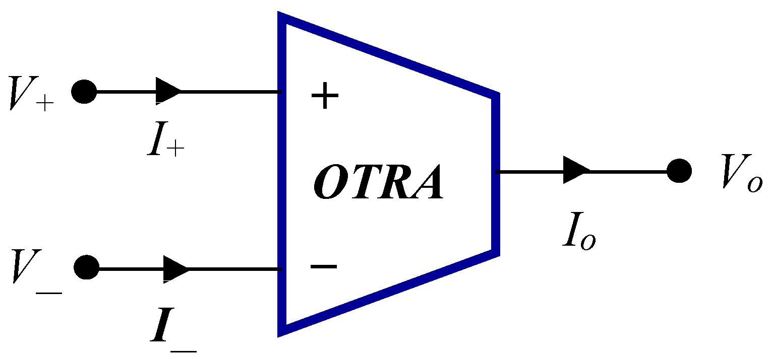
2. Circuit Description and Operation

The OTRA is a three terminal current-mode analog device with two low-impedance input terminals and one low-impedance output terminal [27,28]. The input terminals of the OTRA are virtually grounded, this leads to the circuits that are insensitive to the parasitic capacitances. Figure 2 shows the circuit symbol of the OTRA. The input and output terminal relations of an OTRA can be characterized by the following matrix. For ideal operation, the transresistance gain Rm approaches infinity, forcing the input currents to be equal.
[ V + V V o ] = [ 0 0 0 0 0 0 R m R m 0 ] [ I + I I o ]
V+ = V = 0 and Vo = Rm(I+I)

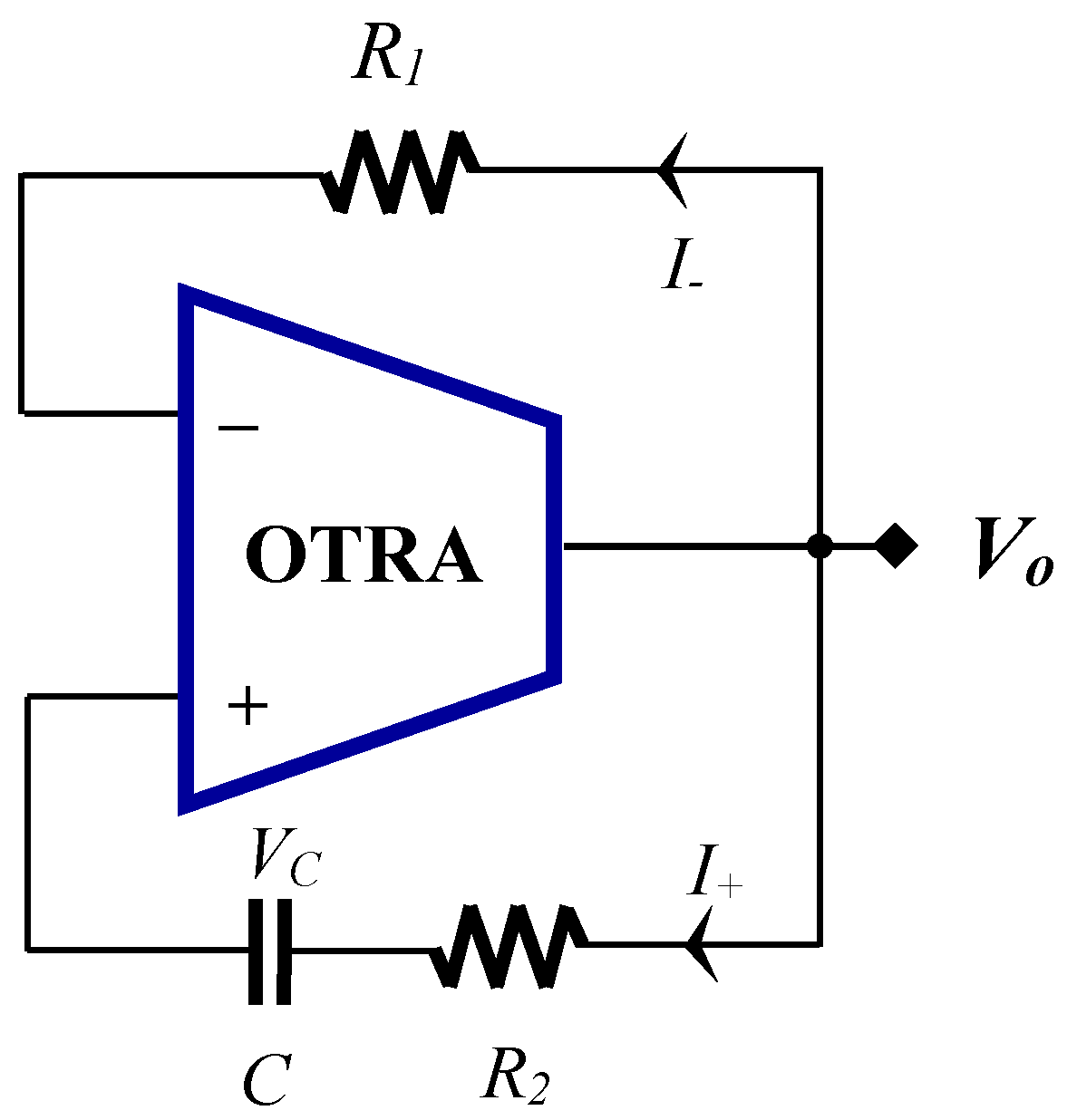
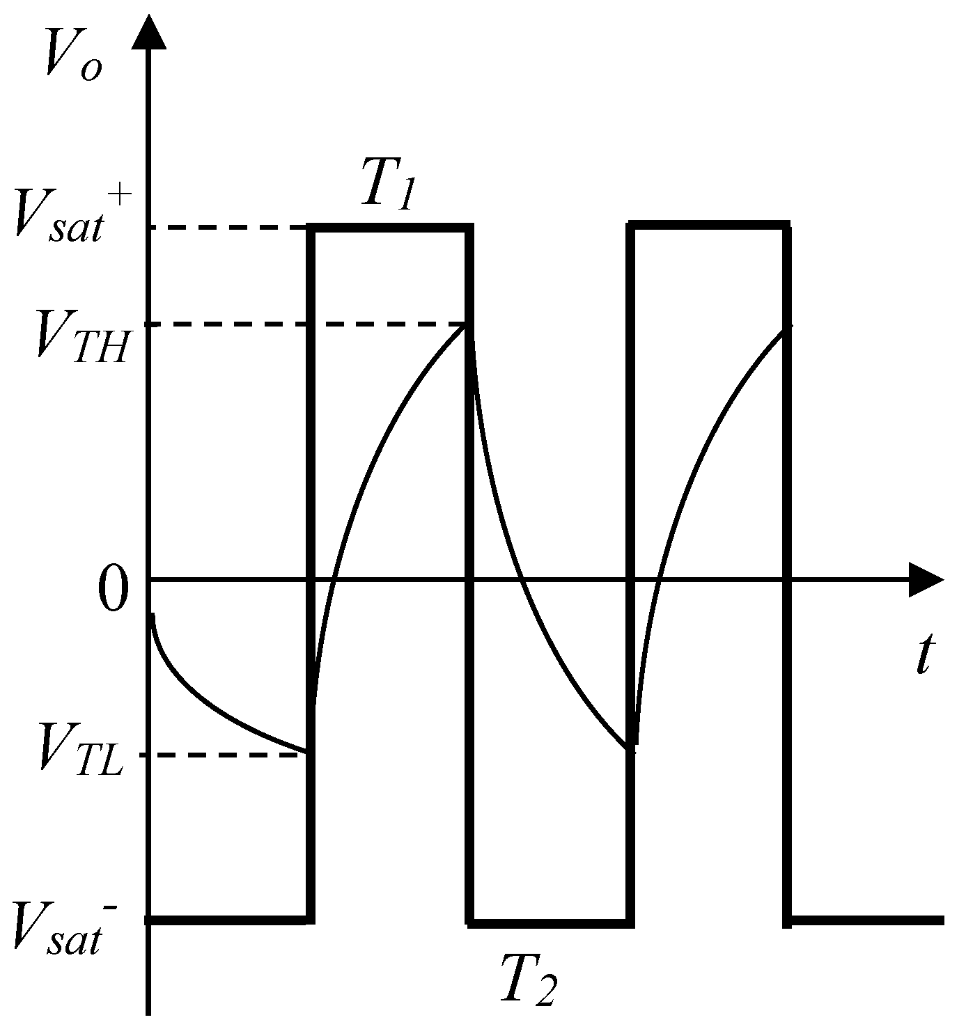
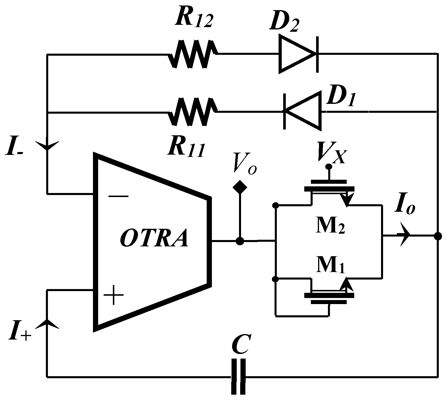
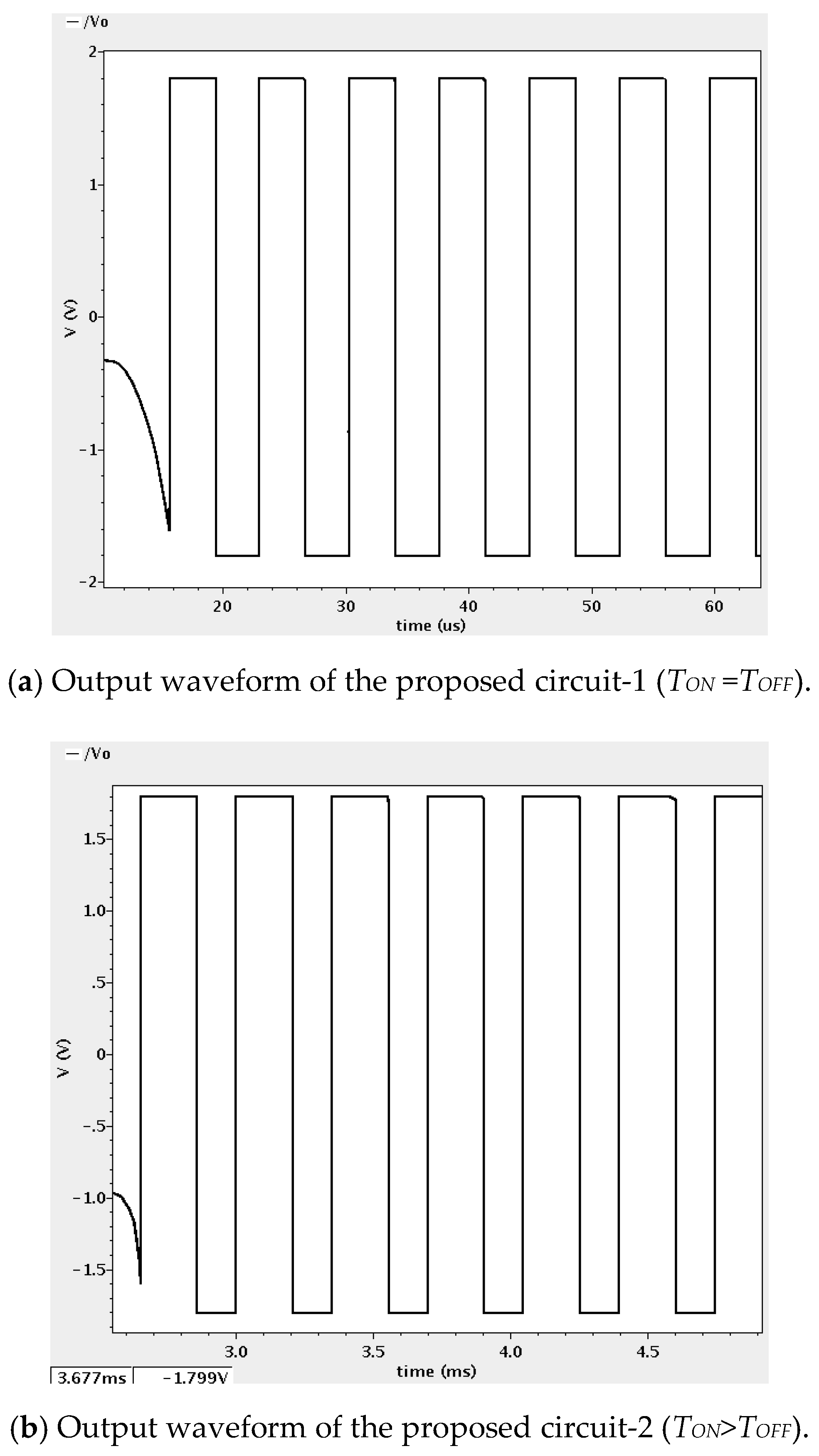
2.1. Proposed Circuit-1

Figure 3 shows the first proposed square-wave generator. This square-wave generator consists of one active element (OTRA), one resistor R1, one capacitor C, and two depletion mode NMOS transistors. The two NMOS transistors M1 and M2 are operated in the triode region and they act as a linear resistor.
Equation (3) depicts the equivalent amount of resistance R2 realized from the parallel combination of NMOS transistors as shown in Figure 4.
R 2 = 1 μ n C o x ( W / L ) ( V X 2 V T )
This circuit generates a square-wave with almost equal and fixed on-duty and off-duty cycles, i.e., 50% duty cycles. Figure 5 shows the corresponding output waveform of the first proposed circuit. From Figure 5, it could be construed that the output square-wave (Vo) has two saturation levels V s a t + and V s a t . Let us assume that Vo is at any one of these two saturation levels. If Vo changes its state from V s a t to V s a t + , it implies that the current at the non-inverting terminal I+ becomes more than the current at the inverting terminal I of the OTRA. At this moment, the voltage VC of the capacitor C begins to increase from the lower threshold value VTL to the final value V s a t + . From Figure 3, the current Io at the output terminal and the current I at the inverting input terminal of the OTRA can be written, as
I o = V o V C R 2
I = V C R 1
Subsequently, the non-inverting input terminal current I+ can be expressed as
I + = V o V C R 2 V C R 1
From the terminal relations presented in Equation (1), Vo changes its state when the non-inverting terminal current is equal to the inverting terminal current I+ = I. The capacitor voltage can be derived from Equations (5) and (6) by putting I+ = I.
V C = ( R 1 / 2 R 2 + R 1 ) V o
The capacitor voltage changes between VTH and VTL. Subsequently, VTH and VTL can be derived from Equation (7) by substituting threshold and saturation values
V T H = ( R 1 / 2 R 2 + R 1 ) V s a t +
V T L = ( R 1 / 2 R 2 + R 1 ) V s a t
The time evolution equation for the capacitor voltage VC, when it starts to increase from VTL towards its final value V s a t + can be expressed as
V C ( t ) = ( V T L V s a t + ) e t R 2 C + V s a t +
Time period T1 can be derived by making V C ( t ) = V T H
T 1 = R 2 C ln ( V T L V s a t + ) / ( V T H V s a t + )
By substituting VTH and VTL values from Equations (8) and (9)
T 1 = R 2 C ln ( R 1 / 2 R 2 + R 1 ) V s a t V s a t + ( R 1 / 2 R 2 + R 1 ) V s a t + V s a t +
From the output waveform, it can be written as
V s a t + = V s a t
T 1 = R 2 C ln ( R 1 / 2 R 2 + R 1 ) 1 ( R 1 / 2 R 2 + R 1 ) 1
T 1 = R 2 C ln ( 1 + ( R 1 / R 2 ) )
The above Equation (15) is meant for on-duty cycle (TON). At the end of the on-duty cycle, the capacitor voltage VC is charged up to the upper threshold voltage VTH, instead of V s a t + . At this point of time, the current at the non-inverting terminal I+ becomes less than the current at the inverting terminal I of the OTRA. Subsequently, the output changes its state from the upper saturation level V s a t + to the lower saturation level V s a t and the capacitor starts discharging. When the voltage across capacitor C starts to decrease from VTH, it can be expressed, as
V C ( t ) = ( V T H V s a t ) e t R 2 C + V s a t
Time period T2 can be derived by setting VC(t) = VTL
T 2 = R 2 C ln ( V T H V s a t / V T L V s a t )
By substituting VTH and VTL values in the above Equation (16) and following the same demonstration as the on-duty cycle T1, we obtain:
T 2 = R 2 C ln ( 1 + ( R 1 / R 2 ) )
The above Equation (18) is for off-duty cycle (TOFF). The final time period (T) of the waveform is the sum of the T1 and T2 cycles.
T = TON + TOFF = T1 + T2
T = 2 R 2 C ln ( 1 + ( R 1 / R 2 ) )
For fixed duty cycles, the R1, R2, and C values will be obtained from the above Equation (19) for a required time period T. The required value of the resistor R2 is calculated from (3) by adjusting the voltage VX.

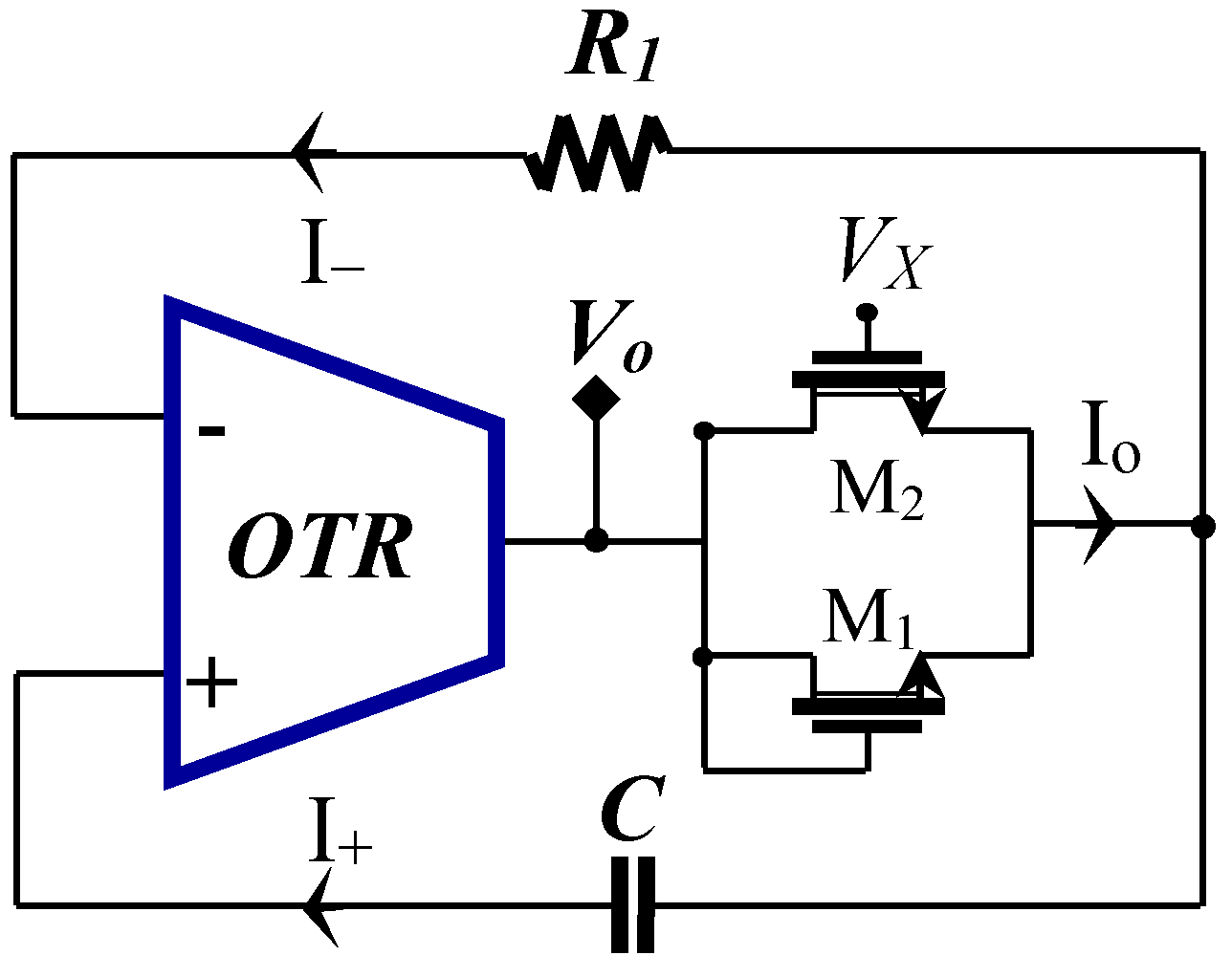
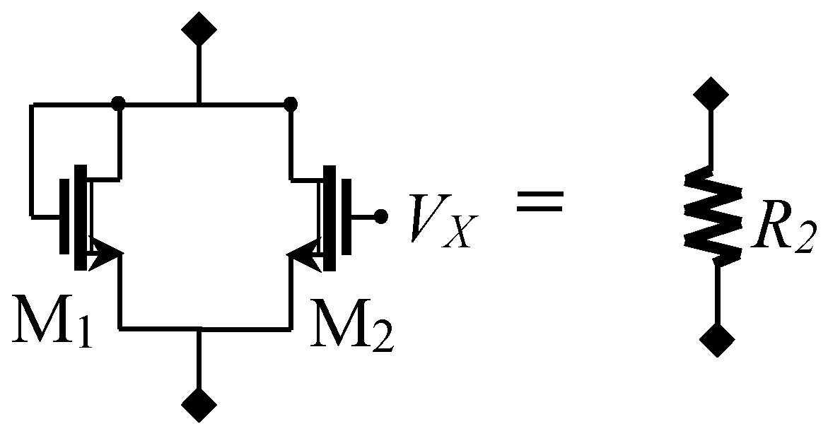
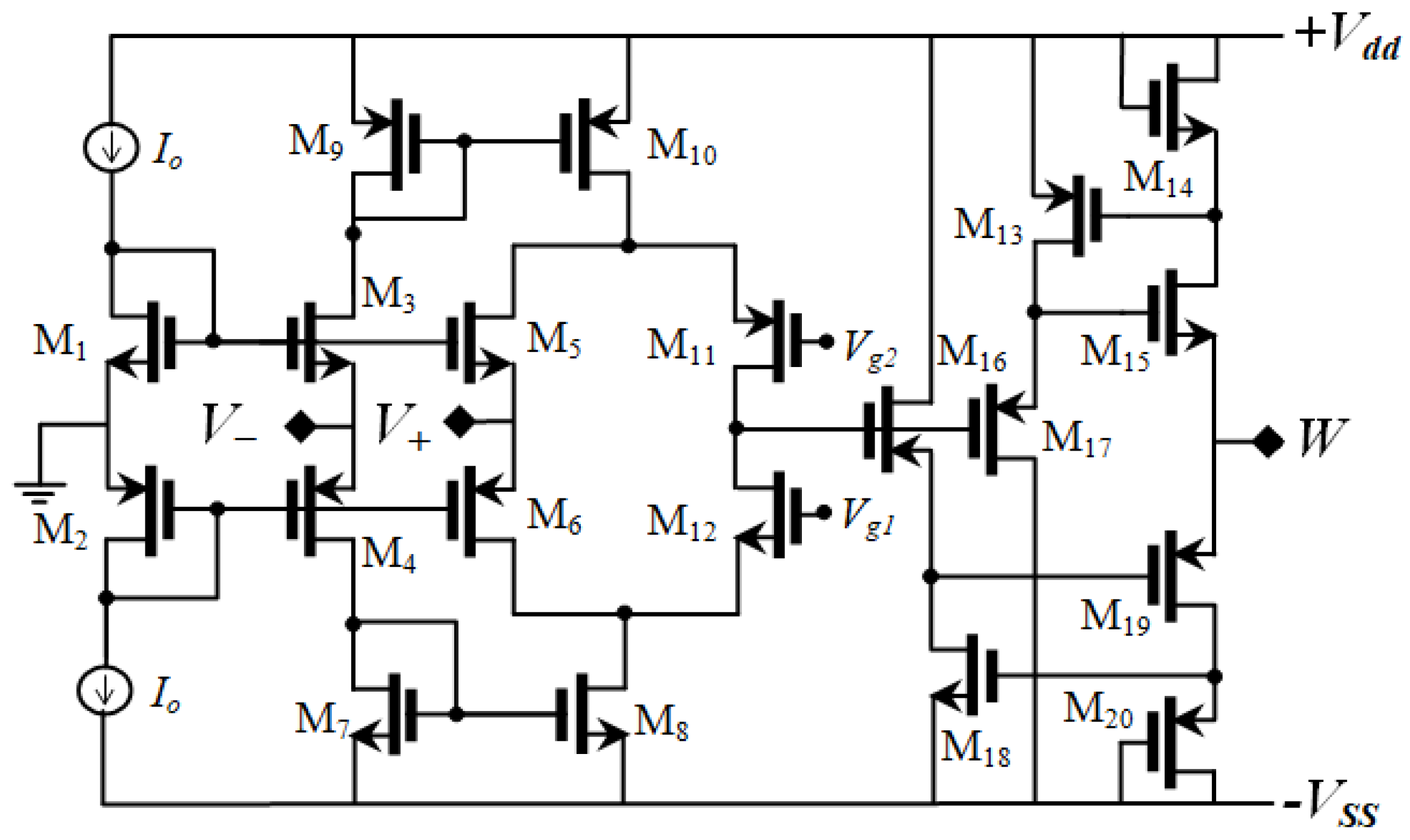
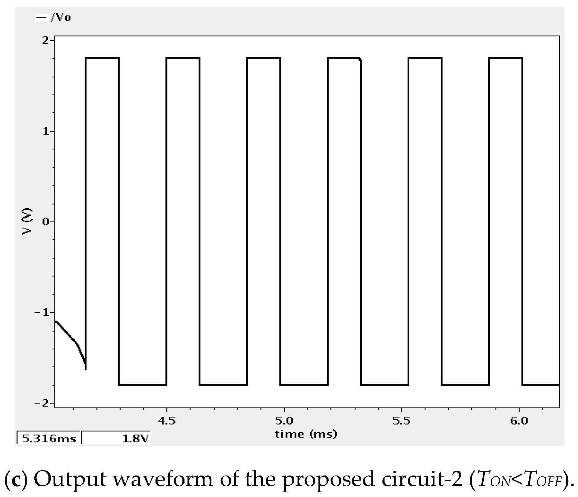
2.2. Proposed Circuit-2

The second proposed circuit that is shown in Figure 6 is designed to vary both the duty cycles independently with the help of resistors R11 and R12. The voltage drops across these resistors used to control the operation of the diodes D1 and D2. The capacitor C starts charging towards V s a t + when non-inverting terminal current is more than the inverting terminal current. This makes diode D1 becomes forward bias and D2 reverse bias. The diode D1 and resistor R11 controls the amount of current at the inverting input terminal. Consequently, the on-duty cycle is more as compared to the off-duty cycle. Similarly, the diode D2 becomes forward bias and D1 reverse bias and capacitor starts discharging towards V s a t + . The resistor R12 and diode D2 controls the inverting input terminal current. Due to this, the off-duty cycle is more when compared to the on-duty cycle.
When considering ideal diodes (zero voltage drop), capacitor threshold voltages can be described by the following equations:
V T H = ( R 12 / 2 R 2 + R 12 ) V s a t +
V T L = ( R 11 / 2 R 2 + R 11 ) V s a t
Time period T1 (TON) can be obtained from Equations (20) and (21), while following the same demonstration reported in Section 2.1 for the proposed circuit-1
T 1 = R 2 C ln ( V T L V s a t + / V T H V s a t + )
T O N = T 1 = R 2 C ln ( ( R 11 / 2 R 2 + R 11 ) V s a t V s a t + ( R 12 / 2 R 2 + R 12 ) V s a t + V s a t + )
T O N = R 2 C ln ( 1 + ( R 11 / R 2 ) )
Similarly for TOFF
T O F F = R 2 C ln ( 1 + ( R 12 / R 2 ) )
The total time period (T) for the proposed square-wave generator in Figure 6 can be expressed as T = TON + TOFF
T = R 2 C ln ( ( 1 + ( R 11 / R 2 ) ( 1 + ( R 12 / R 2 ) )

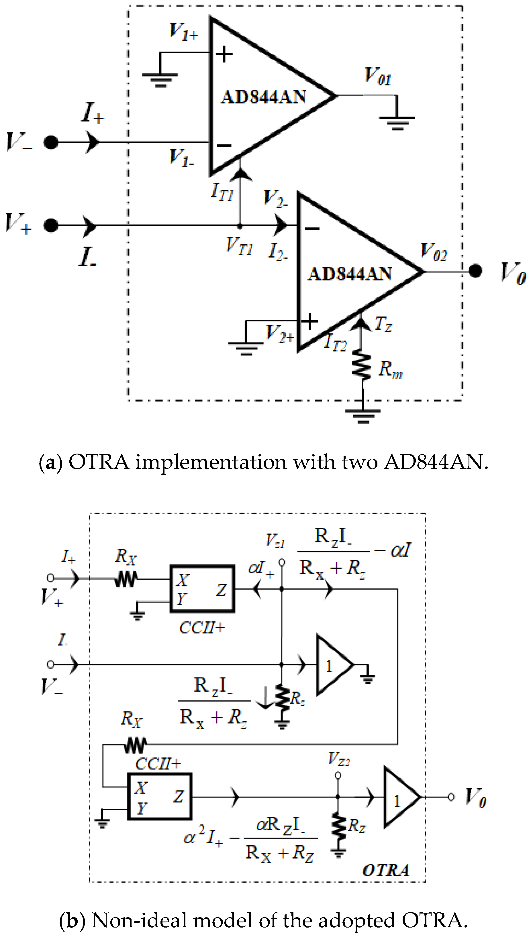
2.3. Non-Ideal Analysis

An equivalent circuit model of the OTRA built with two current feedback amplifiers (CFAs) is shown in Figure 7a to consider the non-ideal and parasitic effects on the proposed circuits.
A practical CFA (AD844AN IC) can be modeled as a positive second-generation current conveyor (CCII+) cascading a voltage buffer with finite parasitic resistances and non-zero current tracking errors. Figure 7a reveals a more detailed circuit model of the OTRA that is given in Figure 7b. Where RX and RZ are the parasitic resistances and α represents the current tracking error factor from the terminal Tz with respect to the inverting terminal. The standard values of RX, RZ, and α are given in AD844AN datasheet are α = 0.98, RX = 50 Ω, and RZ = 3 MΩ. Figure 7a indicates the resultant expressions of the related currents. The voltage tracking error effect between the CCII+ input terminals are skipped (eliminated) in the circuit model, because of the non-inverting terminal for each CCII+ being connected to ground.

2.3.1. Non-Ideal Analysis of Proposed Circuit-1

For the proposed circuits, the non-ideal analysis gives the following equations
V T H = ( α R 1 / ( α R 1 + ( R 2 R Z / R X + R Z ) + R 2 α ) ) V s a t +
V T L = ( α R 1 / ( α R 1 + ( R 2 R Z / R X + R Z ) + R 2 α ) ) V s a t
Substituting these higher and lower threshold voltages into Equations (11) and (17), the non-ideal time period of the proposed circuit in Figure 3 can be expressed, as
T = 2 R 2 C ln ( 1 + ( 2 α R 1 / ( R 2 R Z / R X + R Z ) + R 2 α )

2.3.2. Non-Ideal Analysis of Proposed Circuit-2

The non-ideal equation for the second proposed circuit in Figure 6 is given in Equation (32)
V T H = ( α R 12 / ( α R 12 + ( R 2 R Z / R X + R Z ) + R 2 α ) ) V s a t +
V T L = ( α R 11 / ( α R 11 + ( R 2 R Z / R X + R Z ) + R 2 α ) ) V s a t
T = R 2 C ln ( ( 1 + 2 α R 11 ( R 2 R Z / ( R X + R Z ) ) + R 2 α ) ( 1 + 2 α R 12 ( R 2 R Z / ( R X + R Z ) ) + R 2 α ) )
It can be easily verified that Equations (29) and (32) reduces to Equations (19) and (26), as expected, for ideal OTRA when α ≈ 1 and RX ≈ 0.

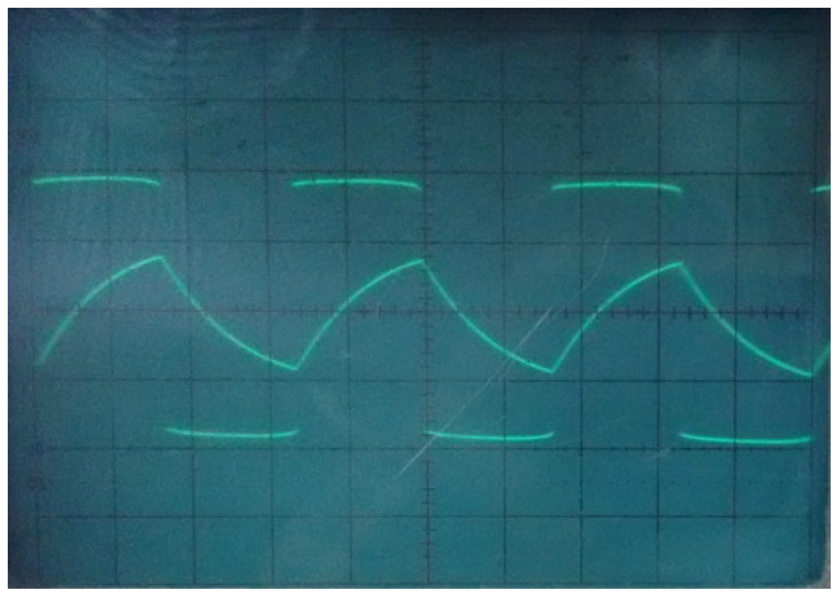
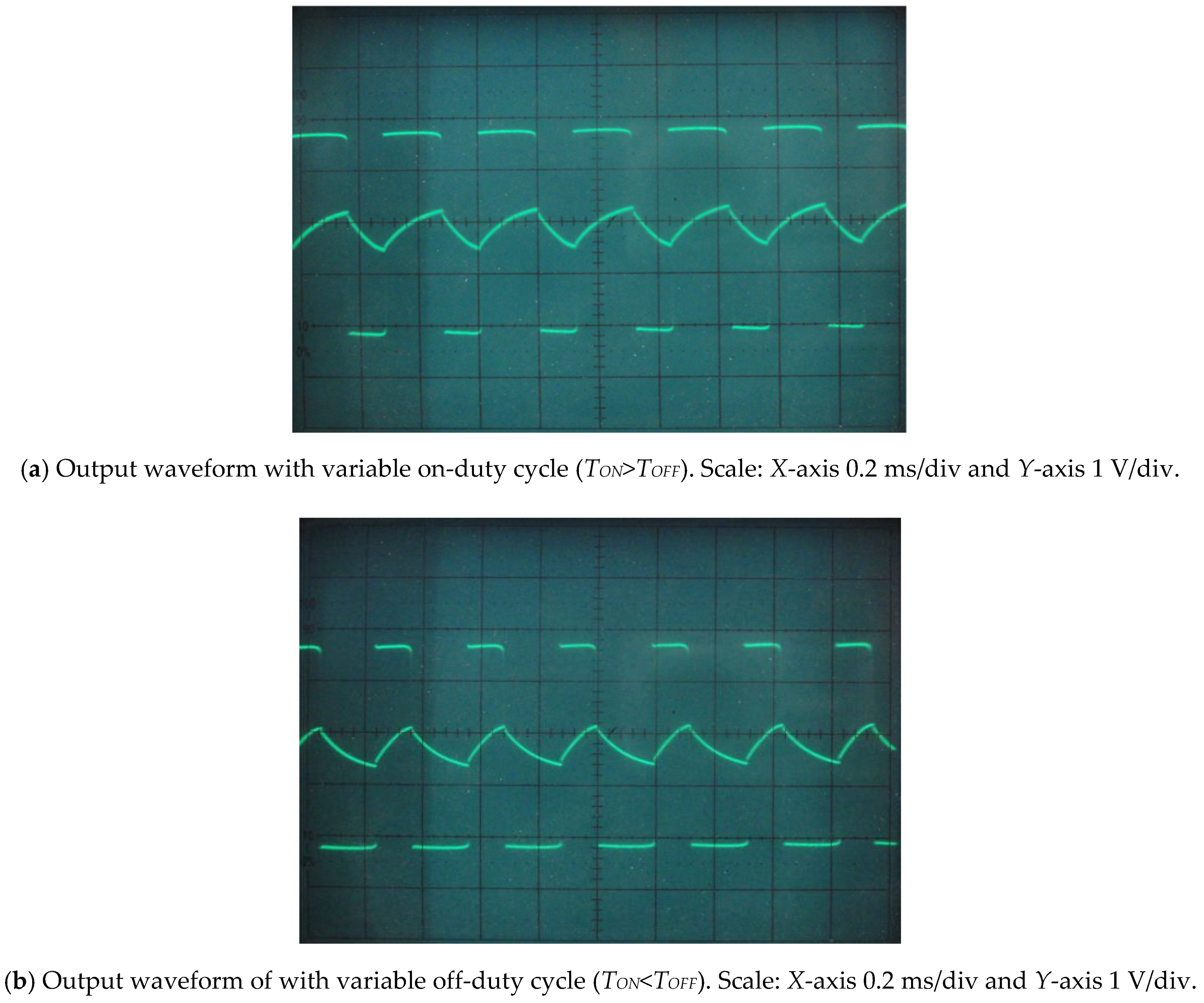
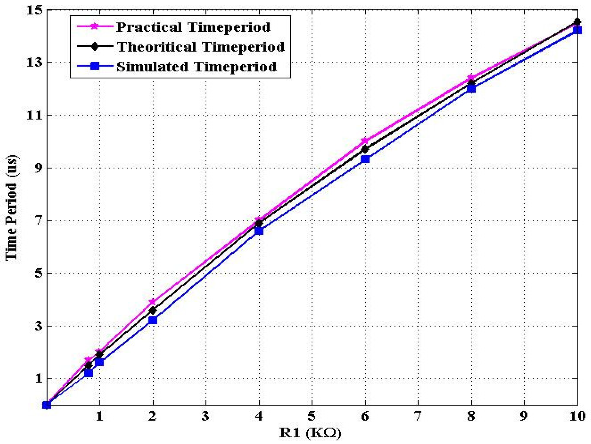
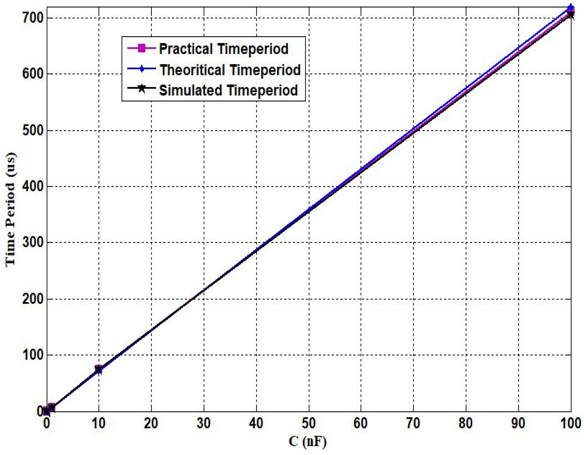
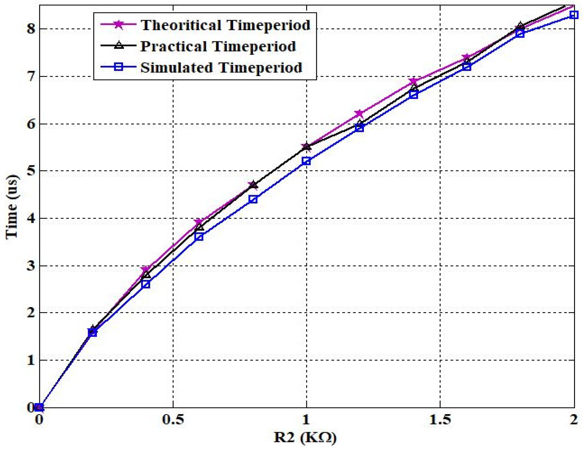
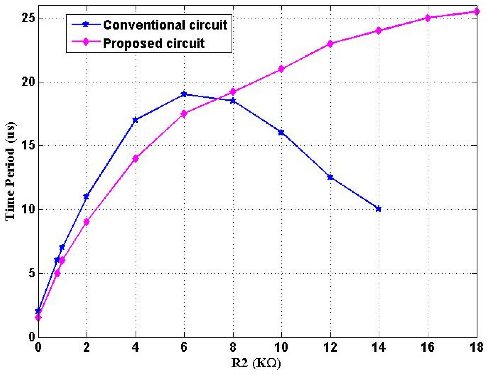
3. Simulation and Experimental Results

The proposed circuits were simulated using SPICE CMOS model parameters with a supply voltage of ±1.8 V. Figure 8 provides the CMOS realization of the OTRA. Table 2 depicts the aspect ratios of the transistors, biasing voltages, and biasing currents. Figure 9 provides the simulated output results of the proposed circuits.
For generating the square-wave of the first proposed circuit in Figure 3, the required time period is chosen first. Subsequently, the ratio of R1/R2 is taken care of and the value of capacitor C is arbitrarily determined from Equation (19). The voltage VX is adjusted to realize the desired value of resistance R2 from (3). However, with this circuit the on-duty and off-duty cycles are fixed. The first proposed circuit was designed with the following passive components R1 = 15 kΩ, R2 = 1.5 kΩ (W = 5μm, L = 180 nm, VX = 80 mV), and C = 1 nF to generate the square waveform. Figure 9a shows the simulated output waveform of the proposed circuit in Figure 3 with a time period of 7.56 µs, which is close to the theoretical time period of 7.19 µs.
For the second proposed circuit in Figure 6, the values of resistors R11 = R12, equivalent resistance R2 and capacitor C, are derived from the above process as stated in fixed duty cycles. Then the resistors R11 and R12 are tuned independently in order to set the required on-duty and off-duty cycles. If resistor R11 is chosen to be greater than the resistor R12, then the on-duty cycle is more than the off-duty cycle. These values will be (R12 > R11) reversed to set the off-duty cycle more than the on-duty cycle. The passive components R2 =1.5 kΩ (W = 5μm, L = 180 nm, VX = 80 mV), R11 = 1.5 kΩ, R12 = 5 kΩ, and C = 0.1µF were used to design the second proposed circuit in Figure 6. Figure 9b,c provide the corresponding simulated output waveforms for the second proposed circuit. From Figure 9b,c, the simulated time period is 0.36 ms, which is close to the theoretical time period of 0.32 ms.
AD844AN is adopted to construct the proposed circuits on a laboratory breadboard in order to verify the theoretical study. The commercial IC AD844AN with current feedback architecture (configuration) is used to implement the OTRA, as shown in Figure 7a [27,28]. Therefore, the behavior of the OTRA is obtained with the schematic shown in Figure 7a. For the proposed circuit in Figure 3, the required time period is chosen first. Subsequently, suitable values of passive components (R1, R2, and C) are derived from Equation (19). In all measurements, the passive component R2 value is the same as the resistance R2 value calculated from Equation (3). For higher sensitivity of the time period with respect to the resistor, the resistor R2 is chosen to be less than 2 kΩ. The experimental output waveform of the proposed circuit-1 is given in Figure 10 with a time period of 7 µs.
Similarly, in the case of the second proposed circuit, the suitable passive component values will be obtained from Equation (26) to a chosen time period. If the required time period is 0.32 ms with 60% on-duty and 40% off-duty cycles then the capacitor C is slightly increased to set the required time period. The resistor R11 and R12 values will be reversed to set the 40% on-duty and 60% off-duty cycles. The output waveforms for the second proposed circuit are given in Figure 11a,b with a time period of 0.31 ms.
Several experiments were performed on the laboratory bread board to test the tunability of the proposed circuits against the passive components R1, R2, and C. The results are presented in Figure 12, Figure 13, Figure 14 and Figure 15 for the proposed circuit configuration in Figure 3. The supply voltage of ±6 V was used for all measurements on tunability.
Figure 12, Figure 13 and Figure 14 denote the time period variation against the passive components R1, R2, and C. For the tunability of resistor R1, the selected passive component values are R2 = 12 kΩ and C = 1 nF and R1 was varied from 800 Ω to 10 kΩ.
A linear like variation of time period was exhibited by the circuit and it is presented in the form of plot in Figure 12. Similarly, for the capacitor C, the selected parameter values are resistors R1 = 15 kΩ and R2 = 1.5 kΩ. The capacitor C was varied from 0.1 nF to 100 nF. Figure 13 plots the practical and theoretical time period variation against the capacitor C. Likewise, for the resistor R2, the circuit was built with resistor R1 = 15 kΩ, capacitor C = 1 nF and R2 was varied from 200 Ω to 3 kΩ.
From Figure 12, Figure 13 and Figure 14, the variation of the time period with respect to the passive components is linear. Figure 1 shows the OTRA based square-wave generator proposed in [28]. For generating the square-wave in the circuit shown in Figure 1, it is necessary to maintain the resistor R2 value less than the resistor R1 and as it will not generate the waveform when R1 < R2. The proposed circuits in Figure 3 and Figure 6 will generate the waveform independent of the resistor values and exhibit more linear curve than the conventional circuit in Figure 1. Figure 15 shows the comparison between conventional OTRA square-wave generator circuit [28] and proposed square-wave generator circuit in Figure 3. For the plot in Figure 15 the parameters values are R1 = 15 kΩ and C = 1 nF, and R2 was varied from 200 Ω to 18 kΩ. From Figure 15, it can be construed that the proposed circuit exhibits more linear curve than the conventional circuit. The proposed circuits can generate the oscillations up to 1.2 MHz. A detailed tally of the proposed circuit with the other square-wave generators in the literature are presented in Table 3 in order to highlight the advantage of the proposed circuit in Figure 3. Form this comparison table, the proposed circuit outperforms with most of the listed square wave generators. The square waveform generators reported in [12,15] generates a high frequency of oscillations when compared with the proposed circuits. With two active components along with passive component consume a high amount power and occupy large silicon area. The square wave generator that is given in [44] requires two passive components (one resistor and one capacitor) and one passive component to produce high frequency oscillations. However, the active device Dual-X Current Conveyor Transconductance Amplifier (DXCCTA) is very bulky with eight input terminals and one output terminal. The total number of transistors to construct the DXCCTA is also large. A greater number of transistors and input terminals increase the silicon area and power consumption.

4. Conclusions

In this paper, two new square-wave generators are proposed. These circuits use only one OTRA and a few passive components, the proposed circuits are simpler than the voltage-mode (op-amp based) waveform generators. The attentive features of these topologies are that they are realized while using commercially available ICs AD 844 AN. The proposed circuits exhibit linear variation of the time period with respect to the passive component. Additionally, the time period of the proposed circuits can be electronically tuned by adjusting the voltage (VX). The results exhibited by such topologies congruent with the simulated as well as the theoretical values. The proposed circuits can generate oscillations up to 1.2 MHz (experimental). These circuits can be expected to find wider applications in many applied electronics, communications, instrumentation, and signal processing applications.

Author Contributions

Circuit implementation, software and hardware validation, investigation, resources, data curation, P.C.S.; writing—original draft preparation, writing—review, corrections and editing, supervision, A.S. All authors have read and agreed to the published version of the manuscript.

Funding

This research received no external funding.

Conflicts of Interest

The authors declare no conflict of interest.

References

  1. Sedra, A.S.; Smith, K.C. Microelectronic Circuits; Oxford University Press: New York, NY, USA, 2004. [Google Scholar]
  2. Sedra, A.S.; Roberts, G.W.; Gohh, F. The current conveyor: History, progress and new results. IEE Proc. Circuits Dev. Syst. 1990, 137, 78–87. [Google Scholar] [CrossRef]
  3. Zafar, Z.N.; Maktoomi, M.A.; Hashmi, M.S. A new adjustable square/triangular-wave generator using CCII/CCCII and OTA. In Proceedings of the 26th International Conference on Microelectronics (ICM), Doha, Qatar, 14–17 December 2014; pp. 104–107. [Google Scholar] [CrossRef]
  4. Kubanek, D.; Khateb, F.; Vrba, K. Current controlled square/triangular wave generator with MO-CCDVCC. In Proceedings of the International Conference on Telecommunications and Signal processing (TSP), Rome, Italy, 2–4 July 2013; pp. 444–448. [Google Scholar] [CrossRef]
  5. Biolek, D.; Biolkova, V. Current-Mode CDTA-based Comparators. In Proceedings of the International Conference on Electronic Devices and Systems (EDS-IMAPS2006), Brno, Czech Republic, 14 September 2006; pp. 1–5. [Google Scholar]
  6. Siripruchyanun, M.; Wardkein, P. A full independently adjustable, integrable simple current controlled oscillator and derivative PWM signal generator. IEICE Trans. Fund. Electron. Commun. Comp. Sci. 2003, E86-A, 3119–3126. [Google Scholar]
  7. Sotner, R.; Jerabek, J.; Herencsar, N.; Lahiri, A.; Petrzela, J.; Vrba, K. Practical Aspects of Operation of Simple Triangular and Square Wave Generator Employing Diamond Transistor and Controllable Amplifiers. In Proceedings of the 36th International Conference on Telecommunications and Signal Processing(TSP 2013), Rome, Italy, 2–4 July 2013; pp. 431–435. [Google Scholar] [CrossRef]
  8. Janecek, M.; Kubanek, D.; Vrba, K. Voltage-Controlled Square/Triangular Wave Generator with Current Conveyors and Switching Diodes. Int. J. Adv. Telecommun. Electrotech. Signals Syst. 2012, 1, 1–4. [Google Scholar] [CrossRef]
  9. Chien, H.-C. Voltage-controlled dual slope operation square/triangular wave generator and its application as a dual mode operation pulse width modulator employing differential voltage current conveyors. Microelectr. J. 2012, 43, 962–974. [Google Scholar] [CrossRef]
  10. Kumbun, J.; Siripruchyanun, M. MO-CTTA-based electronically controlled current-mode square/triangular wave generator. In Proceedings of the 1st International Conference on Technical Education (ICTE2009), Bangkok, Thailand, 21–22 January 2010; pp. 158–162. [Google Scholar]
  11. Srisakul, T.; Silapan, P.; Siripruchyanun, M. An electronically controlled current-mode triangular/square wave generator employing MO-CCCCTAs. In Proceedings of the 8th Int. Conf. on Electrical Engineering/Electronics, Computer, Telecommunications, and Information Technology, Khon Kaen, Thailand, 17–19 May 2011; pp. 82–85. [Google Scholar]
  12. Sotner, R.; Jerabek, J.; Herencsar, N. Voltage Differencing Buffered/Inverted Amplifiers and Their Applications for Signal Generation. Radioengineering 2013, 22, 490–504. [Google Scholar]
  13. Sotner, R.; Jerabek, J.; Herencsar, N.; Prokop, R.; Vrba, K.; Petrzela, J.; Dostal, T. Simply Adjustable Triangular and Square Wave Genrator Employing Controlled Gain Current and Differential Voltage Amplifier. In Proceedings of the 23th International Conference Radioelektronika Pardubice, Pardubice, Czech Republic, 16–17 April 2013; pp. 109–114. [Google Scholar] [CrossRef]
  14. Sotner, R.; Jerabek, J.; Herencsar, N.; Dostal, T.; Vrba, K. Design of Z-copy controlled-gain voltage differencing current conveyor based adjustable functional generator. Microelectron. J. 2015, 46, 143–152. [Google Scholar] [CrossRef]
  15. Haque, A.S.; Hossain, M.M.; Davis, W.A.; Russell, H.T., Jr.; Carter, R.L. Design of sinusoidal, triangular, and square wave generator using current feedback operational amplifier (CFOA). In Proceedings of the IEEE Proc. Region 5 Technical, Professional and Student Conference, Kansas City, MO, USA, 17–20 April 2008; pp. 1–5. [Google Scholar] [CrossRef]
  16. Abuelmaatti, M.T.; Al-Shahrani, S.M. New CFOA-based triangular/square wave generator. Int. J. Electron. 1998, 84, 583–588. [Google Scholar] [CrossRef]
  17. Srinivasulu, A. Current conveyor based relaxation oscillator with tunable grounded resistor/capacitor. Int. J. Des. Anal. Tools Integr. Circuits Syst. 2012, 3, 1–7. [Google Scholar]
  18. Malik, S.; Kishore, K.; Sharma, D.; Maharana, M.; Akbar, S.A.; Islam, T. A CCII-based wide frequency range square/triangular waver generator. In Proceedings of the International Conference on Recent Trends in Information System (ReTIS), Kolkata, India, 9–11 July 2015; pp. 446–449. [Google Scholar] [CrossRef]
  19. Pal, D.; Srinivasulu, A.; Pal, B.B.; Demosthenous, A.; Das, B.N. Current conveyor-based square/triangular waveform generators with improved linearity. IEEE Tran. Instrum. Meas. 2009, 58, 2174–2180. [Google Scholar] [CrossRef]
  20. Marcellis, A.D.; Claudia, D.C.; Giuseppe, F.; Vincenzo, S. A CCII-based wide frequency range square waveform generator. Int. J. Cir. Theory. Appl. 2011, 41, 1–13. [Google Scholar] [CrossRef]
  21. Re Stefano, D.; Marcellis, A.D.; Ferri, G.; Stornelli, V. Low voltage integrated astable multivibrator based on a single CCII. In Proceedings of the IEEE Microelectronics and Electronic Conference Bordeaux, France, Prime, Bordeaux, France, 2–5 July 2007; pp. 177–180. [Google Scholar] [CrossRef]
  22. Chung, W.S.; Kim, H.; Cha, H.W.; Kim, H.J. Triangular/square-wave generator with independently controllable frequency and amplitude. IEEE Tran. Instrum. Meas. 2005, 54, 105–109. [Google Scholar] [CrossRef]
  23. Chen, J.; Tsao, H.W.; Chen, C. Operational transresistance amplifier using CMOS technology. Electron. Lett. 1992, 28, 2087–2088. [Google Scholar] [CrossRef]
  24. Salama, K.N.; Soliman, A.M. CMOS operational transresistance amplifier for analog signal processing applications. Microelectron. J. 1999, 30, 235–245. [Google Scholar] [CrossRef]
  25. Lo, Y.K.; Chien, H.C. Switch controllable OTRA based square/triangular waveform generator. IEEE Trans. Circuits Syst. 2007, 54, 1110–1114. [Google Scholar] [CrossRef]
  26. Lo, Y.K.; Chien, H.C. Single OTRA-based current-mode monostable multivibrator with two triggering modes and a reduced recovery time. IET Circuits Dev. Syst. 2007, 1, 257–261. [Google Scholar] [CrossRef]
  27. Lo, Y.K.; Chien, H.C.; Chiu, H.G. Switch controllable OTRA-based bistable multivibrator. IET Circuits Dev. Syst. 2008, 2, 373–382. [Google Scholar] [CrossRef]
  28. Hou, C.L.; Chien, H.C.; Lo, Y.K. Square wave generators employing OTRAs. IEE Proc. Circuits Dev. Syst. 2005, 152, 718–722. [Google Scholar] [CrossRef]
  29. Chen, J.J.; Tsao, H.W.; Liu, S.I.; Chiu, W. Parasitic-capacitance insensitive current-mode filters using operational transresistance amplifiers. IEE Proc. Circuits Dev. Syst. 2001, 142, 186–192. [Google Scholar] [CrossRef]
  30. Analog Devices Inc. AD844 Current Feedback Op-Amp Data Sheet; Analog Devices Inc.: Norwood, MA, USA, 1990. [Google Scholar]
  31. Cam, U.A. A novel single-resistance-controlled sinusoidal oscillator employing single operational transresistance amplifier. Anal. Integr. Circuits Signal Process. 2002, 32, 183–186. [Google Scholar] [CrossRef]
  32. Singh, A.K.; Gupta, A.; Senani, R. OTRA-basedmulti-function Inverse filter configuration. Int. J. Adv. Electr. Electron. Eng. 2017, 15, 846–856. [Google Scholar] [CrossRef]
  33. Bhatt, V.; Benjwal, P.; Joshi, M. OTRA based second order universal filter and it optimization like Butterworth, Chebyshev and Bessel. In Proceedings of the 2nd International Conference on Research in Intelligent and Computing in Engineering (RICE-2017), Gopeshwar, India, 24–26 March 2017; pp. 143–150. [Google Scholar] [CrossRef] [Green Version]
  34. Singh, A.K.; Senani, R.; Gupta, A. OTRA, its implementations and applications: A state-of-the-art review. Anal. Integr. Circuits Signal Process. 2018, 97, 281–311. [Google Scholar] [CrossRef]
  35. Gurumurthy, K.; Pandey, N.; Pandey, R. OTRA based second and third order sinusoidal oscillators and their phase noise performance. AIP Conf. Proc. 2017, 1859, 020017. [Google Scholar] [CrossRef]
  36. Pandey, N.; Kumar, V.; Goel, A.; Gupta, A. Electronically tunable LC high pass ladder filter using OTRA. ICTACT J. Microelectron. 2017, 3, 446–451. [Google Scholar] [CrossRef]
  37. Nagar, B.C.; Paul, S.K. Lossless grounded FDNR simulator and its applications using OTRA. Analog Integr. Circuits Signal Process. 2017, 92, 507–517. [Google Scholar] [CrossRef]
  38. Shaker, P.C.; Srinivasulu, A. Four new oscillators using operational transresistance amplifier. Radio Electron. Commun. Syst. 2017, 60, 206–214. [Google Scholar] [CrossRef]
  39. Nagar, B.C.; Paul, S.K. Single OTRA based two quadrant analog voltage divider. Analog Integr. Circuits Signal Process. 2018, 94, 161–169. [Google Scholar] [CrossRef]
  40. Komanapalli, G.; Pandey, N.; Pandey, R. New Realization of third order sinusoidal oscillator using single OTRA. AEU Int. J. Electron. Commun. 2018, 93, 182–190. [Google Scholar] [CrossRef]
  41. Komanapalli, G.; Rajeshwari, P.; Neeta, P. New Electronically tunable low-frequency quadrature oscillator using operational transresistance amplifier. IETE J. Res. 2020, 1–9. [Google Scholar] [CrossRef]
  42. Kaur, G.; Ansari, A.Q.; Hashmi, M.S. Fractional order high pass filter based on operational transresistance amplifier with three fractional capacitors of different order. Adv. Electr. Electron. Eng. 2019, 17, 155–166. [Google Scholar] [CrossRef]
  43. Babanezhad, J.N.; Temes, G.C. A linear NMOS depletion resistor and its application in an integrated amplifier. IEEE J. Solid State Circuits 1984, 19, 932–938. [Google Scholar] [CrossRef]
  44. Chaturvedi, B.; Atul, K. Fully electronically tunable and easily cascadable square/triangular wave generator with duty cycle adjustment. J. Circuits Syst. Comput. 2019, 28, 1950105. [Google Scholar] [CrossRef]
  45. Nagalakshmi, K.; Srinivasulu, A.; Ravariu, C.; Vijay, V.; Krishna, V.V. A novel simple schmitt trigger circuit using CDTA and its application as a square-triangular waveform generator. J. Mod. Technol. Eng. 2018, 3, 205–216. [Google Scholar]
Figure 1. Conventional Operational Trans-resistance Amplifier (OTRA) based square-wave generator [28].
Jlpea 10 00012 g001
Figure 2. OTRA symbol.
Jlpea 10 00012 g002
Figure 3. The first proposed current-mode square-wave generator configuration.
Jlpea 10 00012 g003
Figure 4. Resistor realization using two NMOS transistors [43].
Jlpea 10 00012 g004
Figure 5. Output waveform of the proposed square-wave generators.
Jlpea 10 00012 g005
Figure 6. The second proposed square-wave generator configuration.
Jlpea 10 00012 g006
Figure 7. OTRA Equivalent Model [25,26,27,28,29,30,31].
Jlpea 10 00012 g007
Figure 8. The device level circuit diagram of the OTRA [31].
Jlpea 10 00012 g008
Figure 9. Output waveforms of the proposed square-wave generators.
Jlpea 10 00012 g009aJlpea 10 00012 g009b
Figure 10. Output waveform with almost equal and fixed duty cycles (TON = TOFF). Scale: X-axis 2 µs/div and Y-axis 1 V/div.
Jlpea 10 00012 g010
Figure 11. Experimental output waveforms of the second proposed circuits.
Jlpea 10 00012 g011
Figure 12. Variation of time period against resistor R1.
Jlpea 10 00012 g012
Figure 13. Tunability against capacitor C.
Jlpea 10 00012 g013
Figure 14. Tunability against resistor R2.
Jlpea 10 00012 g014
Figure 15. Time period variation between conventional and proposed circuits against R2.
Jlpea 10 00012 g015
Table 1. Performance comparison of active devices.
ParametersOp-ampCFOACCII+CDBAOTAOTRA
Power Supply0.8 V1.8 V1.8 V1.5 V0.5 V1.8 V
Technology0.18 µm0.18 µm0.18 µm0.18 µm0.18 µm0.18 µm
Power Dissipation190 µW--206 µW194 µW215 µW210 µW
Open Loop Gain66 dB75 dB78 dB85 dB52 dB96 dB
Gain Band Width Product3.4 MHz23 MHz--100 MHz7.5 MHz152 MHz
Table 2. Aspect ratios of the circuit shown in Figure 8.
TableW (µm)L (nm)
M1-M64180
M7-M106180
M11-M1220180
M14, M202180
M13, M1812180
M1512180
M16, M194180
M173.3180
Vg1 = Vg2 = 0.8 V and I0 = 40 µA
Table 3. Comparison of the proposed circuit in Figure 3 with the conventional circuits in the literature.
ReferencesNo. of Active ComponentsNo. of Passive ComponentsTotal ComponentsMaximum Frequency RangeSupply Voltage
[9]2 DVCC4 (1 C & 3 R)6860 kHz±10 V
[12]2 VDIBA3 (1 C & 2 R)52.8 MHz±5 V
[15]2 CFOA5 (1 C & 4 R)715 MHz, 1S±5 V
[16]1 CFOA4 (1 C & 3 R)571 kHz--
[17]3 CCII+7 (1 C & 6 R)10574 kHz±6 V
[19]2 CCII+4 (1 C & 3 R)6260 kHz±5 to ±15 V
[20]2 CCII+6 (1 C & 5 R)8737 kHz±15 V
[21]1 CCII+4 (1 C & 3 R)52 kHz1.5 V, 3I.S.
[22]3 OTA3 (1 C & 2 R)616 kHz±5 V
[44]1 CDTA2 (1 C & 1 R)4600 kHz±2.5 V, 1S
±9 V, 2H
[45]1DXCCTA2 (1 C & 1 R)320.6 MHz±1.25 V, 1S
[28]1 OTRA3 (1 C & 2 R)41.0 MHz±15 V
Proposed
Figure 3 circuit
1 OTRA2 (1 C & 1 R)3+2 NMOS Transistors1.5 MHz, 1S
1.2 MHz,2H
±1.8 V, 1S
±6 V, 2H
1S = Simulation, 2H = Hardware Implementation, 3I.S. = Integrate Solution.

