A Chopper Stabilization Audio Instrumentation Amplifier for IoT Applications


1
College of Computer Engineering and Sciences, Prince Sattam bin Abdulaziz University, P.O. Box 151, Alkharj 11942, Saudi Arabia
2
Lab. de Génie Electrique et Electronique de Paris, Paris-Saclay, CentraleSupélec, CNRS, 91192 Gif-sur-Yvette, France
3
Lab. de Génie Electrique et Electronique de Paris, Sorbonne Université, CNRS, 75252 Paris, France
*
Author to whom correspondence should be addressed.
J. Low Power Electron. Appl. 2020, 10(2), 13; https://0-doi-org.brum.beds.ac.uk/10.3390/jlpea10020013
Submission received: 23 March 2020
/
Revised: 6 April 2020
/
Accepted: 7 April 2020
/
Published: 16 April 2020
Abstract
:A low-noise instrumentation amplifier dedicated to a nano- and micro-electro-mechanical system (M&NEMS) microphone for the use in Internet of Things (IoT) applications is presented. The piezoresistive sensor and the electronic interface are respectively, silicon nanowires and an instrumentation amplifier. To design an instrumentation amplifier for IoT applications, different trade-offs are discussed like power consumption, gain, noise and sensitivity. Because the most critical noisy block is the amplifier, a delay-time chopper stabilization (CHS) technique is implemented around it to eliminate its offset and 1/f noise. The low-noise instrumentation amplifier is implemented in a 65-nm CMOS (Complementary metal–oxide–semiconductor) technology. The supply voltage is 2.5 V while the power consumption is 0.4 mW and the core area is 1 mm2. The circuit of the M&NEMS microphone and the amplifier was fabricated and measured. From measurement results over a signal bandwidth of 20 kHz, it achieves a signal-to-noise ratio (SNR) of 77 dB.
1. Introduction
The Internet of Things (IoT) is now recognized by industry, and in particular the electronics industry, as one of the main engines of growth for the decade to come, if not more. The IoT refers to any application taking advantage of the networking of objects capable of interacting with their environment to measure key parameters of this environment, then to transmit this data for analysis, sometimes in real time, and decision making to control or optimize a system. Detection is the starting point for the IoT and smart home applications. It is also the first problem faced by followers and professional designers. The design of many economical transducers such as accelerometers, force sensors, extensometers and pressure transducers is based on resistive Wheatstone bridges for differential voltages in millivolts (mV). Before going into detail, it is essential to accurately capture these low-level signals and amplify them to levels compatible with analog-to-digital converters (ADCs) without direct current (DC) offset or noise. Likewise, current detection using high potential ammeter shunts requires amplifiers without inputs referenced to ground and capable of tolerating high common mode voltages. Micro-electro-mechanical systems (MEMS) are sensors or actuators whose lateral dimensions and thickness are of the order of a micrometer. For decades until today, MEMS sensors have been manufactured on a large scale for many consumer applications such as aerospace [1], inertial sensors in mobile phones such as gyrometers and accelerometers [2,3], video game controllers and airbag triggers. These devices, which are the basis of research tools [4], have reached a sufficient maturity to be directly developed and integrated by large industrial groups such as STMicroelectronics [5].
In the world of transistors, it is known that the reduction of dimensions mainly allows integrating more devices on a given surface. Therefore, it enables to reduce the manufacturing cost of the transistor, to increase the performance of the integrated circuit, and reduce the operating voltage. With regard to sensors, reduced dimensions are also other benefits that enabled the development of emerging applications. Therefore, since the 2000s, these sensors have been reduced to the nanometer scale with the name nano-electro-mechanical systems (NEMS). These devices allow the study and detection of objects at the molecular scale [6,7] and also at the quantum scale [8]. The constant times are likewise reduced which implies a limited response time only because of the electronics control and not the NEMS itself. In addition, in the nanoscale era, we can see a modification in the intrinsic properties of materials as in silicon nanowires and their thermal and conductive properties modified by the size effect. Hearing implants are technological devices developed to correct hearing loss. Today, the cochlear implant is the most complete system. It implements the fields of acoustics, electronics, signal processing and information, biology, and knowledge of the human physiology. The objective of the microphone is to transduce acoustic waves to an electrical signal. Consequently, it operates in the frequency range from 20 Hz to 20 kHz [9].
The objective of this paper is to implement a nano- and micro-electro-mechanical system (M&NEMS) microphone with a low-noise instrumentation amplifier, which has a high signal-to-noise ratio (SNR) and high unity-gain bandwidth (UGBW). The architecture of the amplifier is carefully selected and some circuit innovations are explored. In addition, a detailed noise analysis of the complete system composed by the M&NEMS microphone and the low-noise amplifier is presented. The complete system is fabricated in 65 nm CMOS process and measurement results are discussed. The rest of the paper is organized as follows. Section 2 presents an overview of our fabricated M&NEMS microphone. Then, Section 3 provides the instrumentation amplifier details. Section 4 presents the measurement results of the fabricated circuit and discussion. Finally, Section 5 concludes the paper.
2. Nano- and Micro-Electro-Mechanical System (M&NEMS) Microphone Design
The fundamental of M&NEMS technology is presented for the first time in 2009 [10]. M&NEMS technology allows designing a novel sensor that combines both MEMS and NEMS structures like the design of a 3D accelerometer sensor [10]. The M&NEMS in-plane accelerometer is shown in Figure 1.
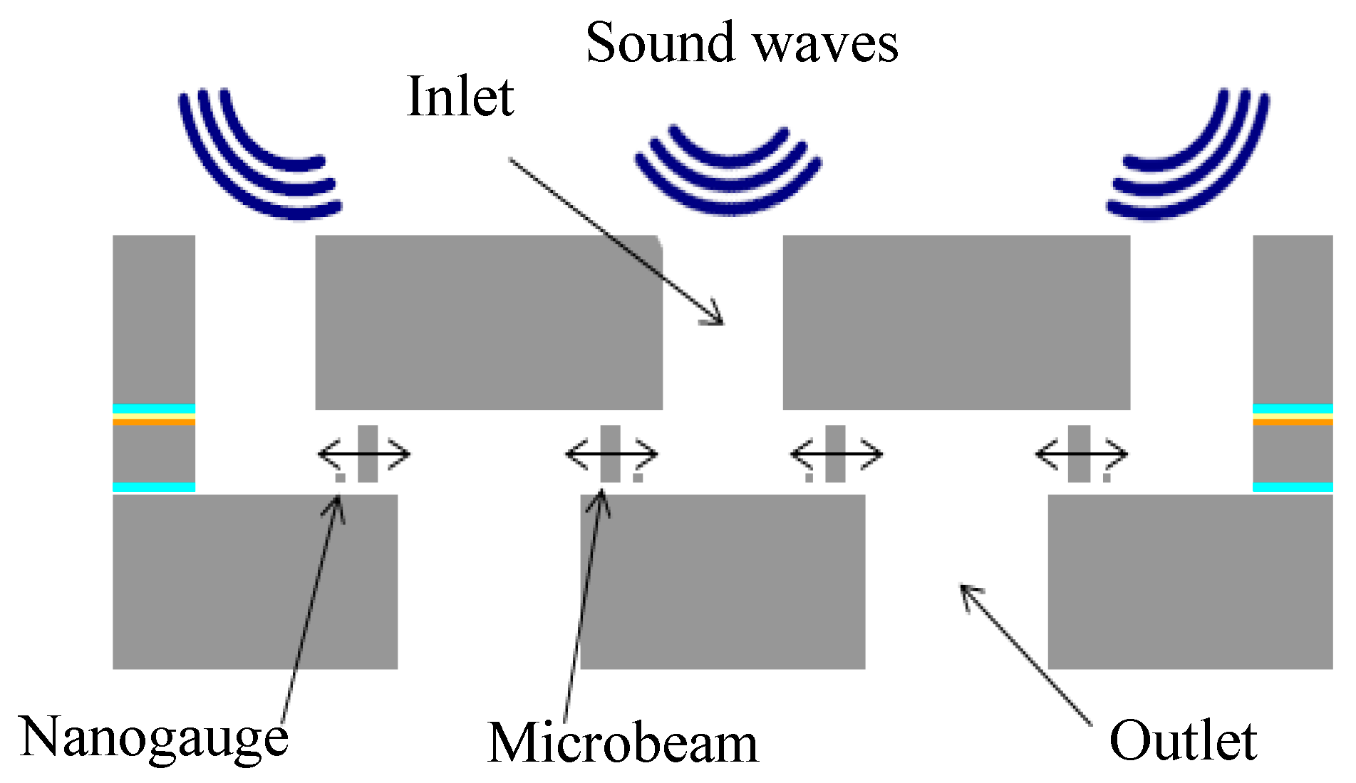
Figure 2 shows the M&NEMS transducer composed of four rigid micro-beams and four suspended silicon nanogauges. All micro-beams are placed between the inlet vents and the outlet vents. Inside the transducer, the inlet vents allows for guiding the sound wave and the outlet vents allows the equilibration of the pressure in a back cavity to be enabled. In addition, the motion of the beams is enabled by micro-slits placed between the beams and both top and bottom wafers.
Therefore, the pressure can easily drop from one side to the other side in the same beam. Inside, the suspended silicon gauges is located the stress that induced by the motion of a beam. It represents a transducer with a resistance variation of each silicon nanogauge. To measure the resistance variation, the four silicon nanogauges are connected as a Wheatstone bridge. If a sound pressure is detected, then two silicon nanogauges will be stretched and two silicon nanogauges will be compressed at the same time. Moreover, random accelerations are automatically self-canceled.
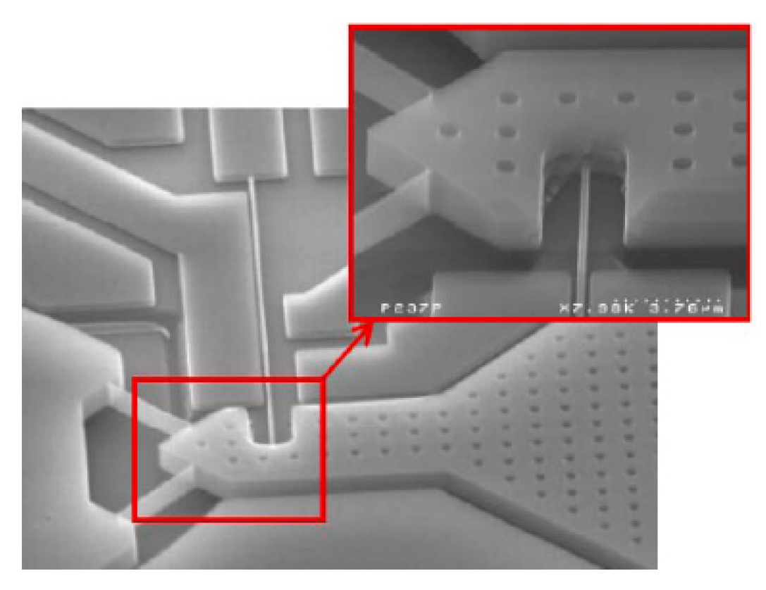
The technological M&NEMS fabrication process is done in the clean room of the CEA-LETI (Atomic Energy Commission-Laboratory of Electronics Information Technology). Figure 3 shows the fabricated M&NEMS accelerometer with zooming on different components like the four silicon nanogauges, the inlet vents and the outlet vents. The detailed analysis of the sensor’s operation allows identifying the constraints dedicated to the bridge itself. Among these constraints, there is the common-mode voltage and the output impedance, as well as the constraints related to the audio application.
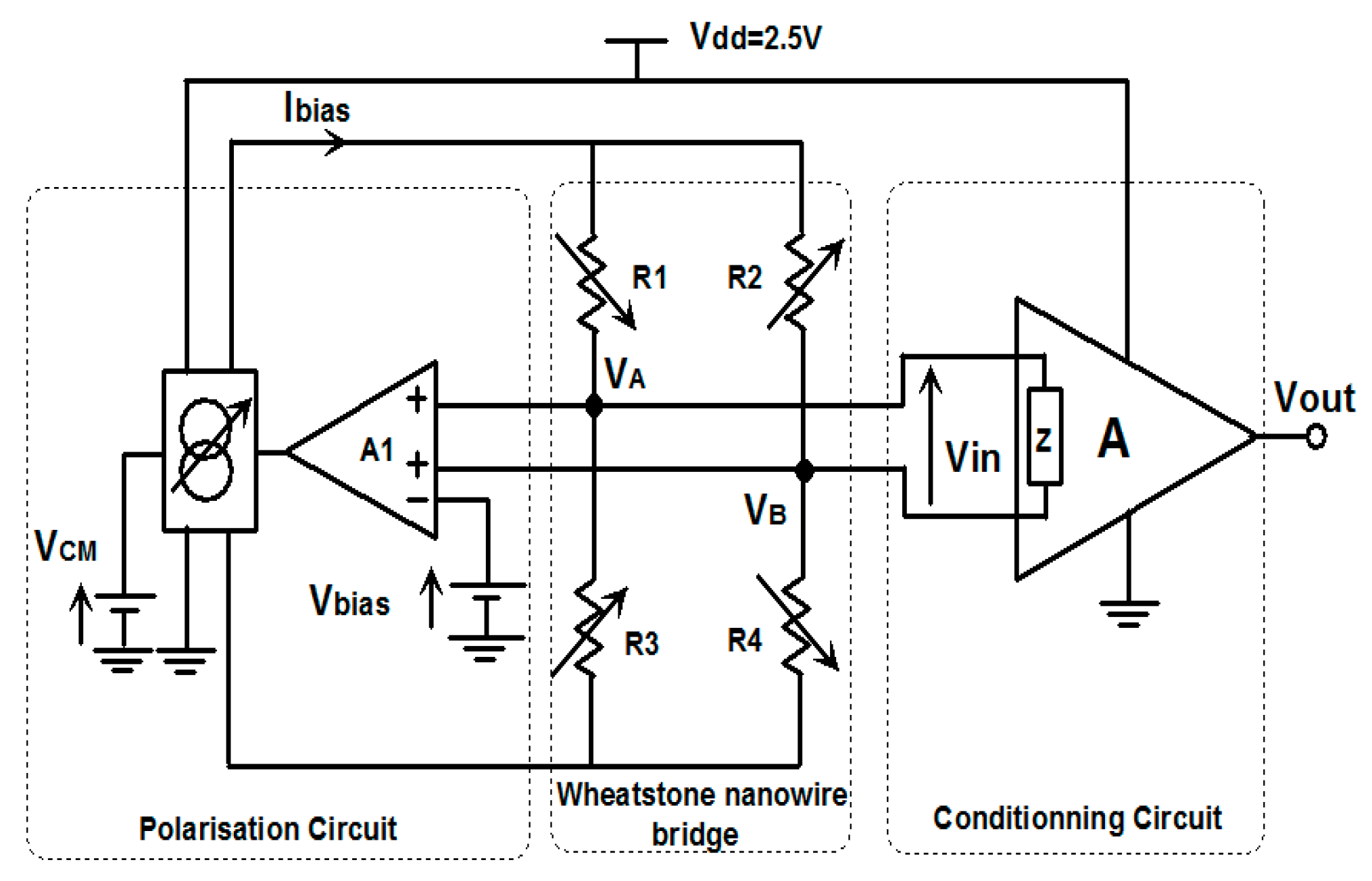
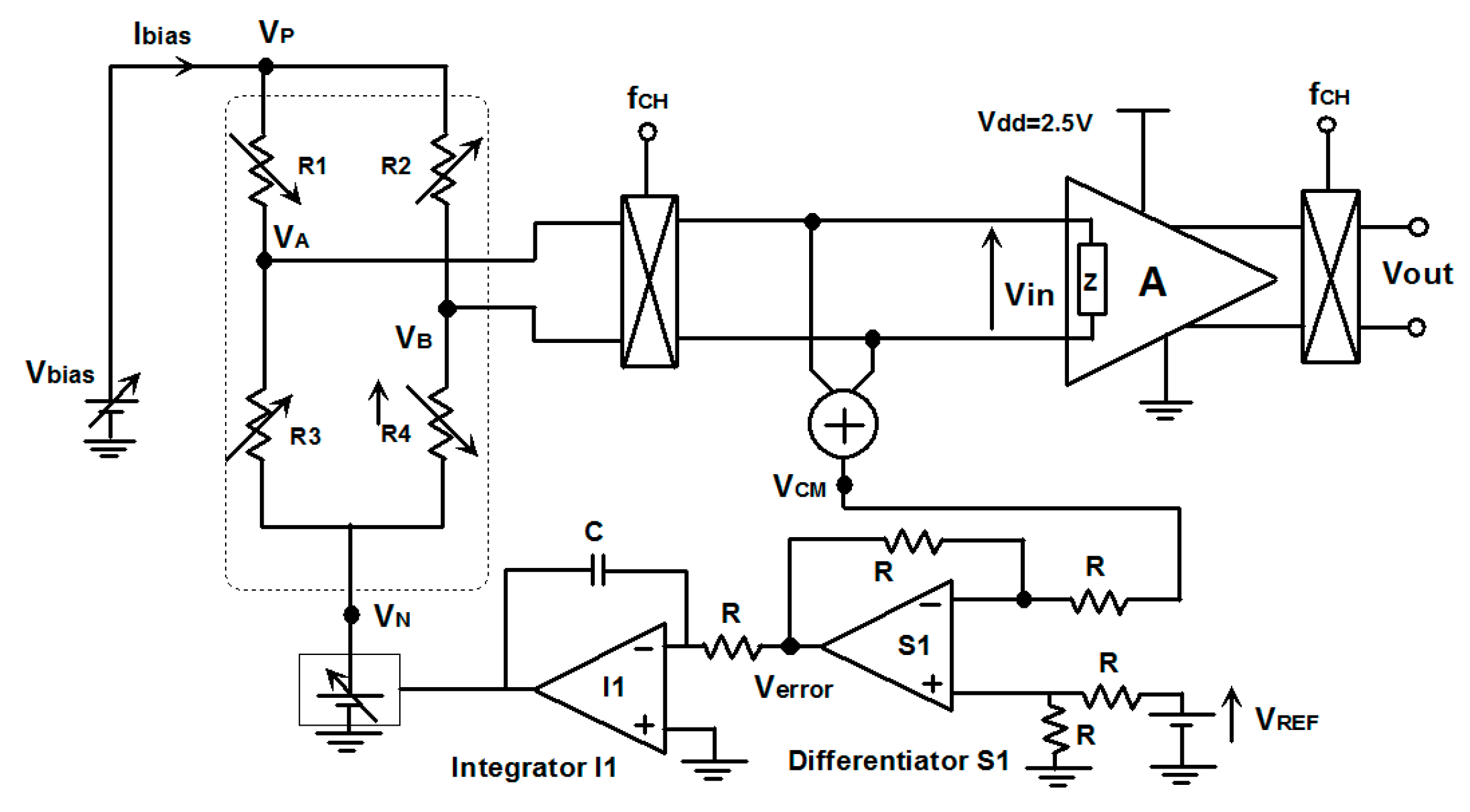
The M&NEMS analog front-end composed by a sensor biasing circuit and an instrumentation amplifier as a read-out circuit is shown in Figure 4. The Wheatstone bridge is composed by the nanowire gauges. It is biased by a voltage-controlled constant current source. Moreover, the common mode voltage of the instrumentation amplifier input is maintained at Vdd/2 with a servo-loop build around A1 that equate source and sink current through the bridge. The differential voltage Vin flowing through the instrumentation amplifier is proportional to the gauge resistance imbalance induced by acoustic vibrations. The power consumption of the electronic circuit is fixed by the current biasing. In the simplest case, the same power supply can bias both sensor and amplifier. In this case, the equivalent resistance RE of the four gages is quite high to maintain a low-power consumption. Moreover, the supply voltage of the complete M&NEMS nanowire sensor is sufficiently small. However, all current integrated circuits in the industry generally operate with supply voltages greater than 1.2-V. This minimum supply voltage of the M&NEMS nanowire sensor generates a bias Ibias of about 279-μA. This bias current corresponds to a power supply of about 335-μW, which is excessive, on the one hand, because the nanowires cannot dissipate it, and on the other hand, it leads to an increase of the total power consumption that is not compatible with the target IoT application. Therefore, it is necessary to add a circuit that controls the voltage bias of the sensor independently of the amplifier supply voltage. The sensor output common-mode voltage might cause problems for the amplifier when the circuit is referenced at 0 V. In fact, for a 100 μA Ibias current, the bias voltage Vbias is 0.4 V. The sensor common-mode voltage VCM is about 0.2 V in this case. This VCM value is assuming the same gauges. Therefore, the amplifier input signals VA and VB evolve around an average value of 0.2 V. With the objective of driving this VCM voltage to a value compatible with that of the amplifier without generating an excessive bias current, it is necessary to control the current of the VCM voltage independently, and therefore to control Vbias as shown in Figure 4.
The voltage Vbias is one of the key parameters of sensitivity as expressed in Equation (1). It can also be considered that at constant sound pressure, the sensitivity affects the power of the output signal. If the Vbias increases, the output voltage also increases. Therefore, the polarization affects the SNR. However, the current flow through the sensor implies power consumption, which is a crucial parameter in battery-powered systems. Therefore, to optimize the sensor polarization, it is relevant to evaluate its SNR according to its power consumption. The impact of the bias voltage on the SNR is evaluated with the noise model. The thermomechanical noise occurs upstream of the bridge. From the models, the power Psignal of the useful signal is related to the voltage Vbias as:
According to the common definition of the SNR with a reference sound pressure of 94 dB-SPL, the SNR of the microphone alone is obtained with the following expression:
where V2Total denotes the total output noise power of the sensor. Therefore, the power consumption Pabsorb depends on the nominal value R0 of one nanogauge and can be written as:
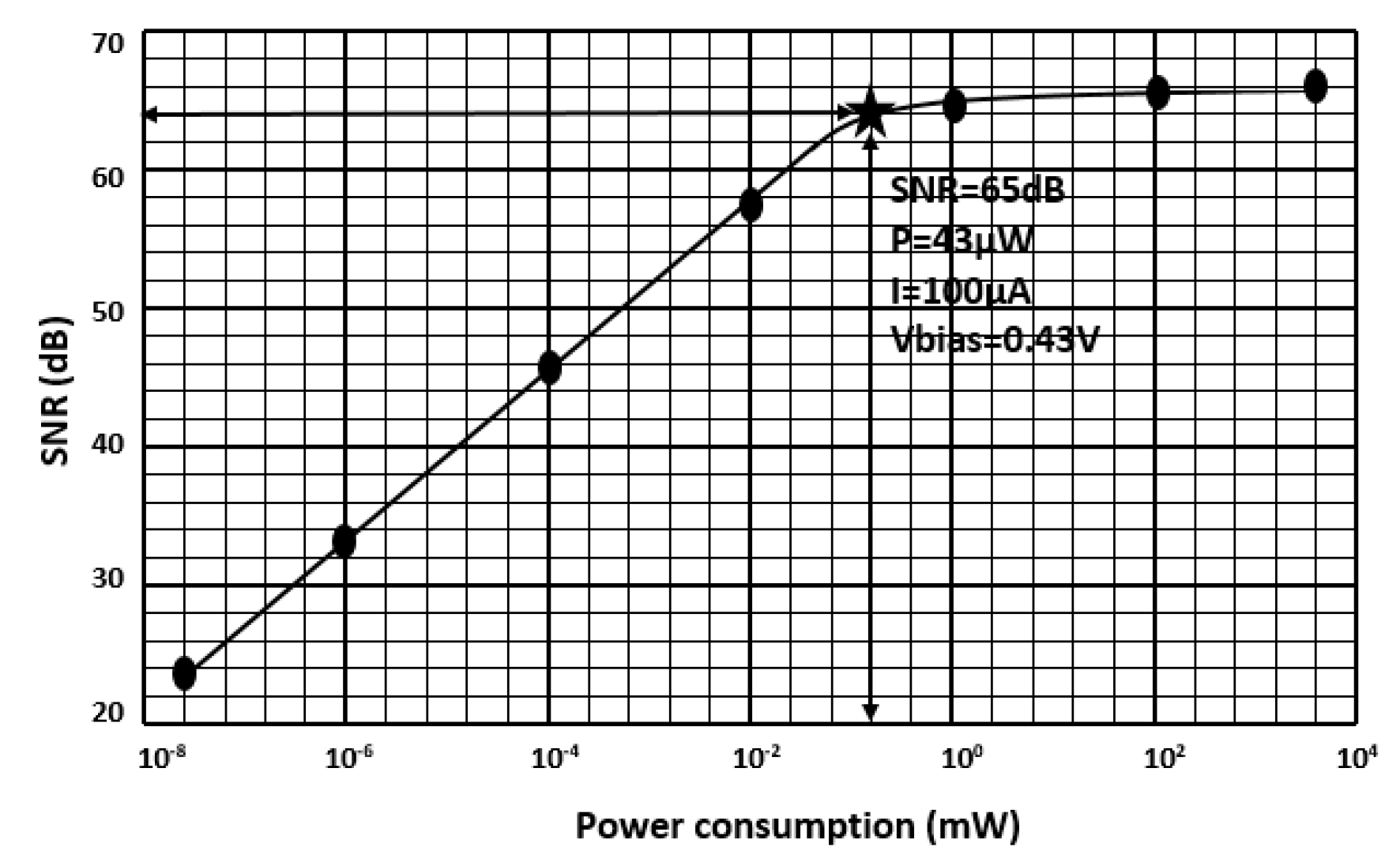
These relations allow us to draw the curve of Figure 5, which shows the SNR evolution according to the supply power absorbed by the bridge. The signal-to-noise ratio reaches its asymptote (SNR Max of the sensor alone 65 dB) when it is polarized with 2 V supply. The operating point of the sensor alone is considered optimal when the SNR stops to increase linearly with the power, from 43 μW.
3. Low-Noise Instrumentation Amplifier Implementation
Integrated circuits dedicated to measuring the resistance of silicon nanogauge in audio applications are not commercially available. Based on circuits already made for similar sensors where a Wheatstone bridge is used, a special instrument was developed. It allows the sensor to operate, demonstrates the relevance of the resistive detection, and studies its performance. Some results can also be used for the design of an integrated circuit. Consequently, the dedicated electronics should allow operating the sensor, to reach these maximum performances and to provide an easily exploitable signal. The integrated circuit must also, and above all, ensure the polarization of the bridge. According to the experimental development step of the nanogauges, the integrated device must propose a regulation of the current and several configurations. Protection functions have been added to preserve the gauges during manipulations. Its use must be easy to multiply the experiments, without the risk of damaging neither a sensor nor the instrument.
Flowing a current through the sensor elements is essential to obtain a signal. The easiest way to do this is to use the feed directly as shown in Figure 6. The use of a servo-control allows maintaining the current biasing independently of both the supply voltage and the value of the nanowire resistors. It also keeps the common mode close to the optimal value required for the proper operation of the amplification stage. The control loop comprises an adder that extracts the common-mode voltage of the bridge, a subtractor S1, an integrator I1, and a generator controlling the voltage VN. The voltage Verror is the error voltage that can be written as:
At equilibrium, Verror = 0 V, then:
Thus, the voltage V’bias across the nanogauges bridge is controlled via the voltage Vbias such that:
This method can also be applied to the current polarization [9]. The diagram is given in Figure 6. The control loop composed by the subtractor S1 followed by the integrator I1 acts on the current IN to cancel the common residual mode voltage VCM generated at the input of the amplifier when there is an imbalance between IP and IN. As a result, at equilibrium, the currents IP and IN are identical. The accuracy required depends on the common-mode tolerance of the amplifier.
This configuration is easily achievable in CMOS technology because a transistor is naturally a voltage-controlled current source. It has the advantage of completely dissociating the useful bias current from the undesired common-mode current. It is enough to control Ibias to master the current that crosses the sensor, and thus its sensitivity. Ibias is a lever for acting on sensitivity.
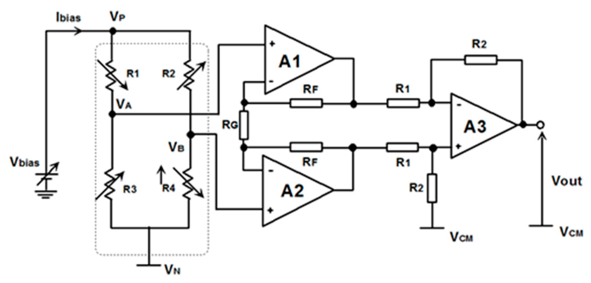
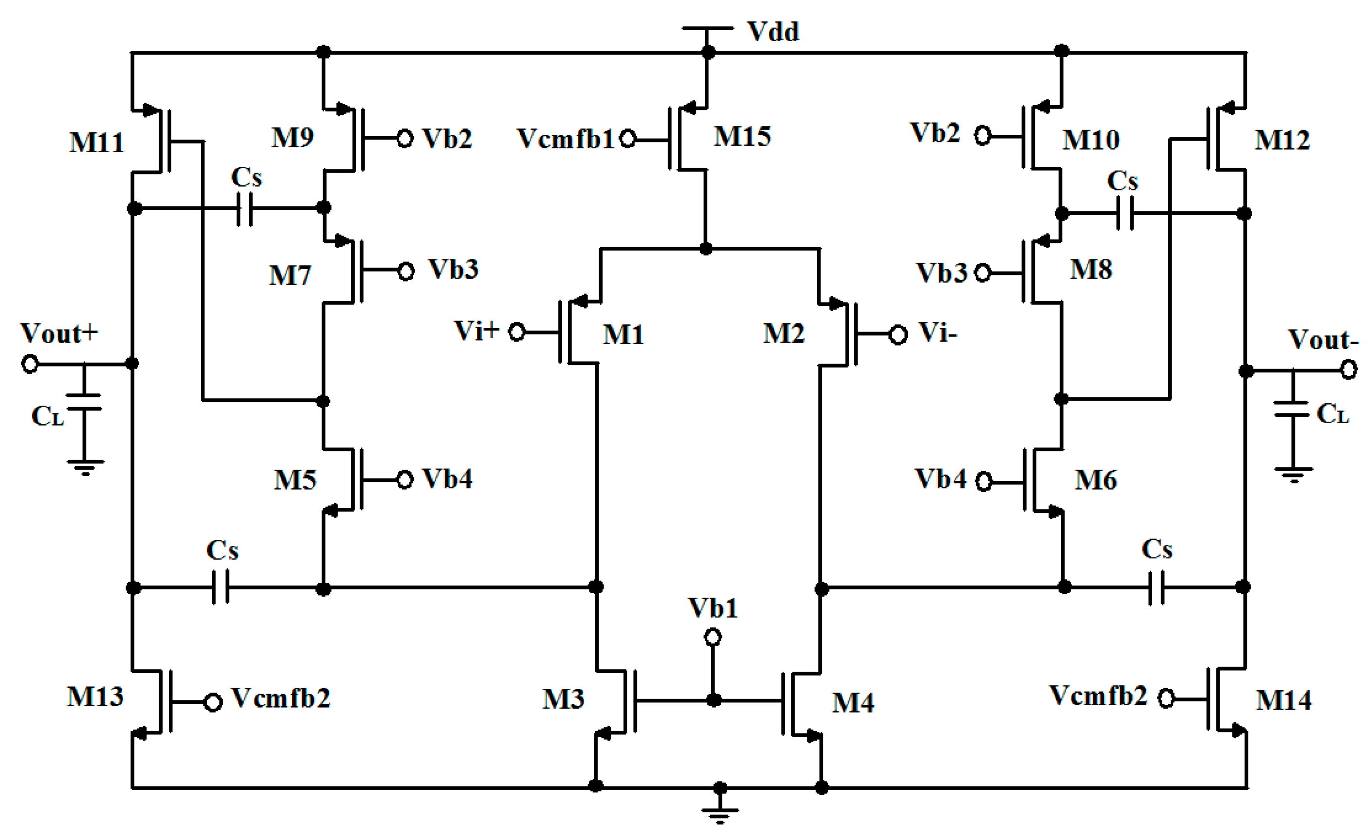
The two-stage instrumentation amplifier structure has the high input impedance required to maintain the sensitivity of the resistive sensor [13]. A low-noise instrumentation amplifier is integrated after the Wheatstone bridge. It processes a voltage signal VA–VB. It is composed of amplifiers A1, A2 and A3 as shown in Figure 7. The architecture of each amplifier is based on a two-stage operational transconductance amplifier (OTA) as shown in Figure 8.
The input stage is directly connected to the sensor. It allows amplifying the difference voltage VA–VB. It is composed of amplifiers A1 and A2 whose intrinsic gain is very high. The associated passive elements RF and RG determine the voltage gain GV1 of the entire stage such that:
The second amplification stage can convert the differential signal into a voltage Vs, referenced to the common-mode voltage. Its gain GV2 depends on the elements R2 and R1 such that:
The total gain GV of the instrumentation amplifier can be written as:
The resistors’ network of the instrumentation amplifier was designed by R1 = 5.1 kΩ, R2 = 160 kΩ, RF = 2 kΩ and RG = 390 Ω. Therefore, the ideal total differential gain GV is 51 dB. Finally, the sensitivity of the sensor is increased by a factor k comprising the product of the gains of the stages of the amplification chain. This simple structure involves the bias voltages VP and VN across the sensor. They define both the current Ibias flowing through it and the common-mode voltage VCM according to Equations (10) and (11) as:
where R0eq is the equivalent resistance of the sensor and Rn is the resistance of element n. The common-mode voltage VCM can be critical for the proper functioning of the sensor and its electronics. It must be located between the supply voltage of the amplifier and the reference voltage to allow the excursion of the output voltages of the sensor without saturating the amplifiers that make up the chain. The value VDD/2 allows the maximum excursion. Therefore, this choice implies conditions on the voltages VP and VN. In the case of a sensor preceded by this amplification, structure supplied with a voltage of 2.5 V, for a polarization current Ibias of 100 μA, with nominal nanogauge resistance R0 of 4300-Ω, the voltage VP must be 1.365 V, VCM of 1.25 V and VN of 1.135 V.
The bandwidth of the instrumentation amplifier is a significant limiting factor. It must be adapted to the sensor and its application [14]. Quantities that change slowly as the temperature or the acceleration does not require the same bandwidth as fast variables as the acoustic vibrations of air. In an instrumentation amplifier, the resulting bandwidth is expressed as a function of the gain-bandwidth product of the operational amplifiers. It will be necessary to find a satisfactory compromise between the gain and the bandwidth by considering the intrinsic limits of the operational amplifiers. Therefore, it is according to one of these conditions that the distribution of the gains in an amplification chain is determined.
To reduce the input-equivalent noise of the instrumentation amplifier, we propose to use the well-known chopper stabilization (CHS) technique. The traditional CHS technique is shown in Figure 9 [15,16]. The signal path mismatch and the demodulated current spikes generate a residual offset Vos. Therefore, alternating current (AC) spike is caused by the mismatch between the capacitances due to clock feed-through at the Chopper clocks transition moments. The first modulator M1 rectify this AC current. Therefore, a DC spike current appears at its input. The resulting DC spike current has an average value Ioffset of:
where ΔC1 and ΔC2 denote the CHS mismatch parasitic capacitance, Vclk denotes the clock signal magnitude and fCH denotes the chopping clock frequency, with fCH = 12-kHz. The chopper series impedance and the input signal source are going through by this noise current. Therefore, it depicts as an input voltage spike. The residual offset Vos resulting from the spike average DC value can be written as:
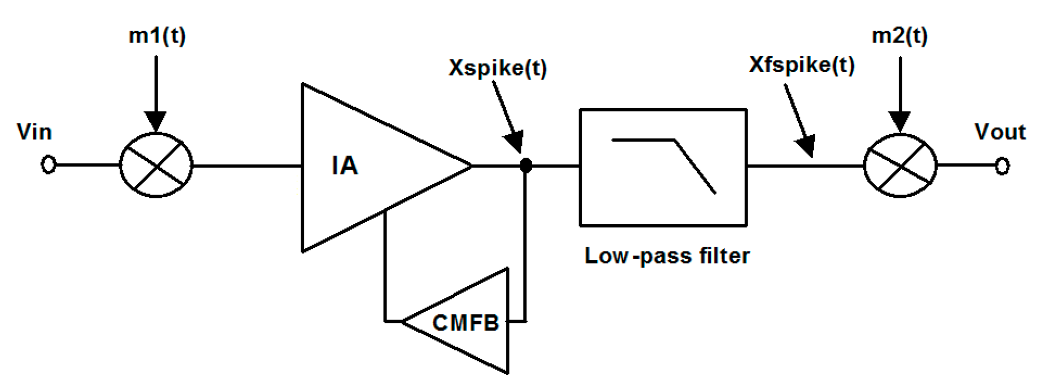
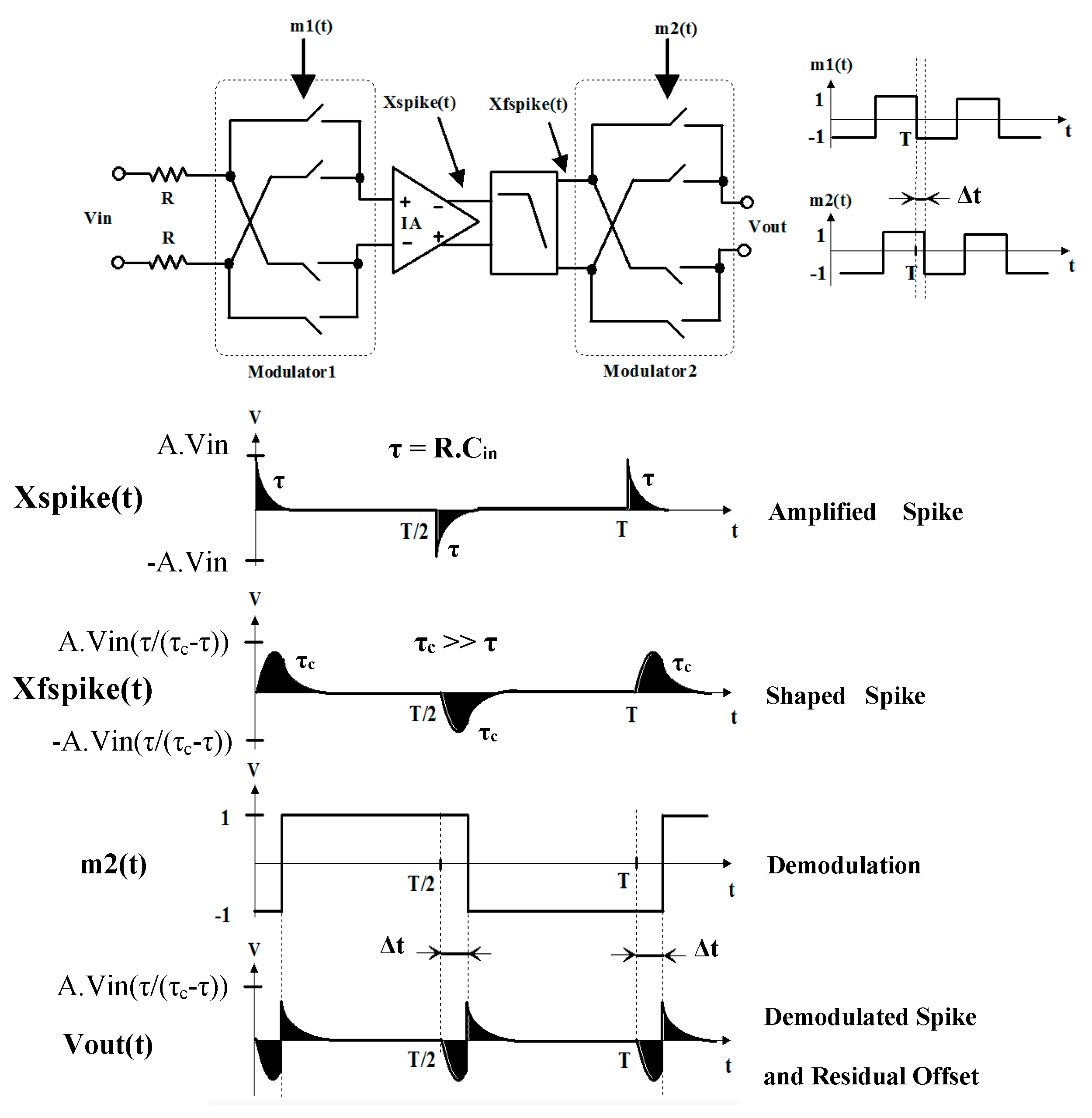
where R denotes the equivalent input impedance. Therefore, a residual offset Vos depicts the spike average DC value. Moreover, a spike voltage Vos is created in the input of Modulator1. This spike voltage causes a low-frequency interference. To cancel-out this interference, the solution is to create a proper delay Δt between Modulator1 and Modulator2. The proposed instrumentation amplifier CHS technique is shown in Figure 10 and Figure 11. The instrumentation amplifier with its common-mode feedback circuit (CMFB) is located between two modulating clock signals m1(t) and m2(t) with period T. Moreover, we introduce a delay ∆t between the two clock signals m1(t) and m2(t) at the same time. Due to the introduction of the delay ∆t, this technique causes a chopping of the spike signal itself. Therefore, the DC content of the output signal Vout(t) is minimized. The residual output dc offset is completely cancelled if an optimal delay value ∆topt exists, which can be written as:
where τ = R × Cin with R denotes the input resistance and Cin denotes the input capacitance of the amplifier. The major weakness of this technique is the τ itself, which not only depends on the sensor’s source resistance R, but also on the amplifier’s input capacitance Cin.
The input modulator’s spike signal is amplified and then multiplied with m2(t) in the demodulator. The resulting output signal Vout(t) then contains, apart from higher order harmonics of the chopping frequency, a DC part or residual offset, which is due to chopping artifacts. To solve this problem, shaping of the spike can be introduced by the addition of a first order low-pass filter with time constant τc after the amplifier. We must have T >> τc >> τ with T is the period of the square wave signal m1(t). The shape of the time response of the filtered spike is primarily determined by τc and independent of the impedance of the connected sensor.
Since the output offset is still linearly dependent on τ, the optimization of ∆topt has been done in such a way that offset reduction is most effective for a worst-case sensor resistance. For our specific implementation ∆topt/τc = 0.8 has been chosen. The low-pass filter has a cut-off frequency of 30 kHz. The nominal chopping frequency is 12 kHz.
4. Measurement Results
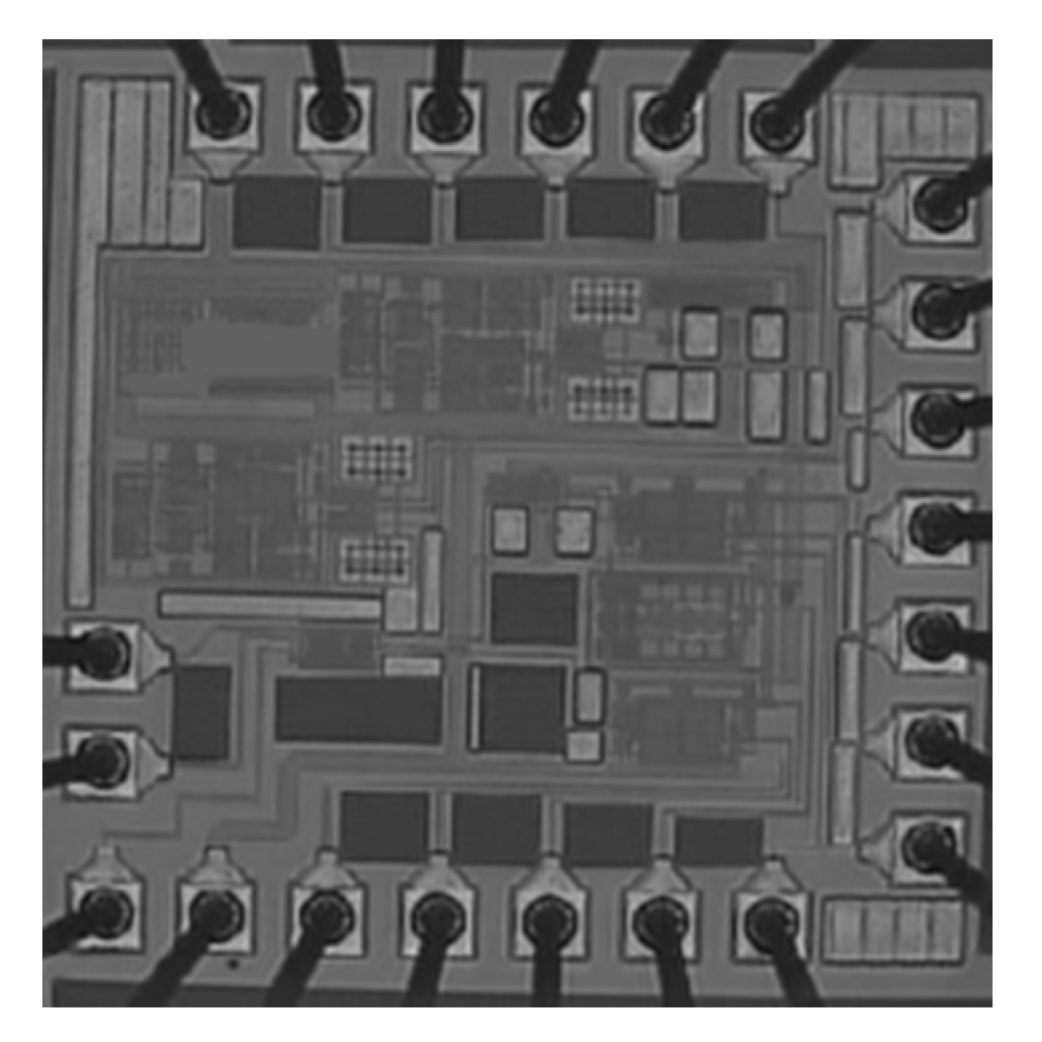
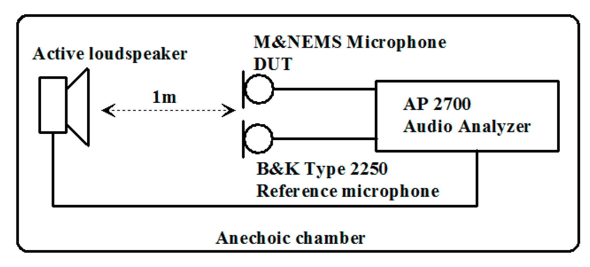
Prototypes of the M&NEMS microphone with the low-noise instrumentation amplifier are fabricated and experimentally characterized. The die microphotograph with the layout view of the instrumentation amplifier is shown in Figure 12. The method of simultaneous comparison is used to perform the measurement of the M&NEMS microphone, as shown in Figure 13. Some measurement devices are used to perform the test of the chip. A calibrated microphone is used as a reference microphone. It is placed near the tested microphone in the objective to compare their outputs. To isolate unwanted external phenomena, an anechoic chamber is used to perform all measurements. A loudspeaker is placed at a distance of one meter in front of the two microphones. The loudspeaker generates a sound with 1 kHz frequency. It is used as a reference point. In the objective to obtain an equal response of loudspeaker at all frequencies, a corrected EQ (equalizer) curve is used. The output of the M&NEMS microphone, as well as the output of the B&K Type 2250 Analyzer (Brüel & Kjær, Nærum, Denmark), are connected to the AP 2700 audio analyzer.
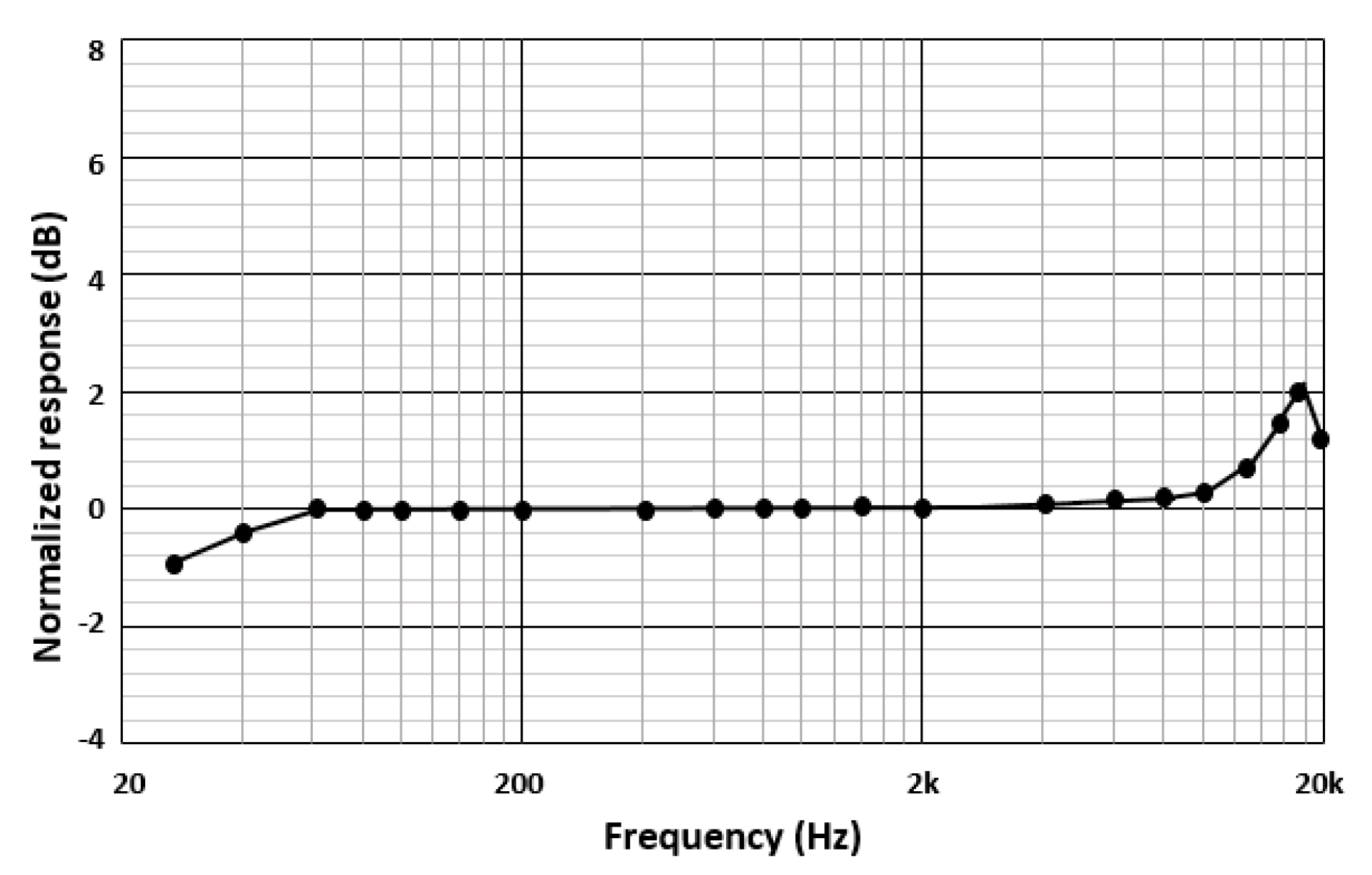
The sound pressure of the loudspeaker is fixed at 94 dB with a frequency of 1 kHz. The B&K analyzer detects the sound pressure level. The 94 dB level corresponds to a 1 Pa acoustic sound pressure level. To obtain a constant level, the frequency response is corrected by the EQ curve. Therefore, the reference microphone frequency is fixed at 1 kHz. The comparison of the level of all other frequencies to the reference frequency is shown in Figure 14. The sound pressure level of 94 dB corresponds to the normalized response of 0 dB. It is clear from Figure 14, the M&NEMS microphone has a flat analog output response to about 20 kHz. After performing the frequency response of the M&NEMS microphone, the measurement of the SNR of the instrumentation amplifier was performed and described below.
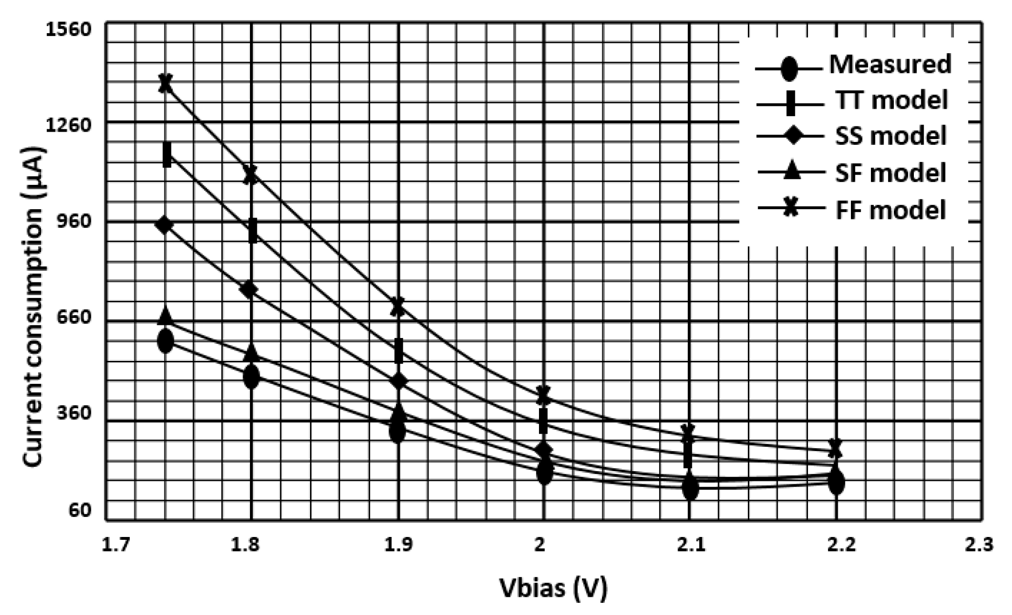
In a first step, to measure the instrumentation amplifier, no signal coming from the M&NEMS microphone is injected at its inputs. The ammeter inserted in the supply circuit to measure the current ISupply consumed by this part of the circuit as a function of the voltage VbiasAI. The measurement results allow us to know the relationship between the current absorbed by the instrumentation amplifier as a function of the bias voltage Vbias. The curve plotted with experimental data and those obtained with the results of simulations for different models of transistors are shown in Figure 15 for comparison. Simulation results are performed in three processes and temperature corners as TT for Typical-Typical, FF for Fast-Fast and SS for Slow-Slow. The curve observed experimentally is similar to that obtained in the simulation with the SF-transistor model. Therefore, the deviation observed when the current exceeds 160 μA can be attributed to the presence of an underestimated access resistance during the simulation. This first characterization identifies the transistor model closest to that of the transistors integrated into the chip.
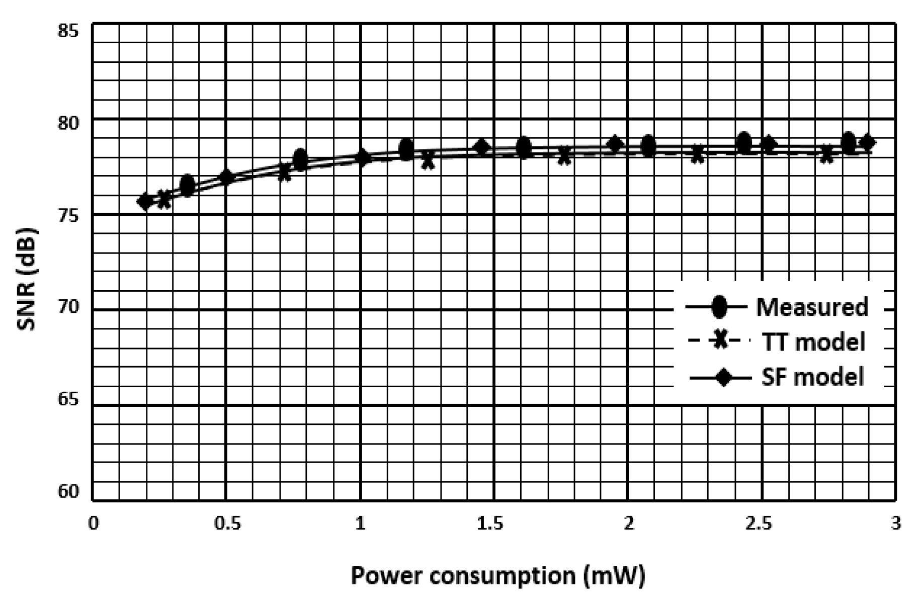
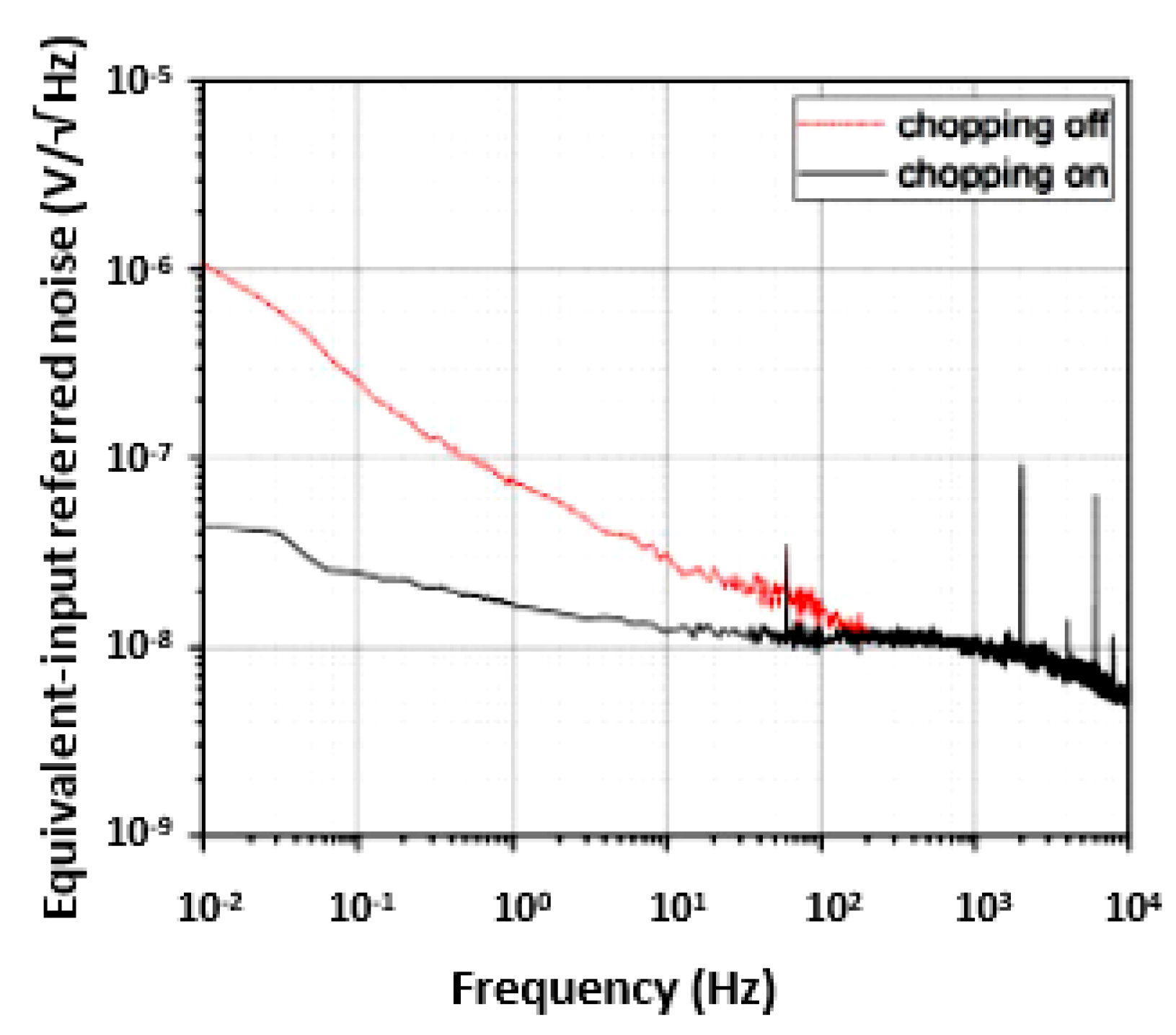
The curves in Figure 16 show the SNR of the complete system as a function of the amplifier power consumption. Simulation results have been added for comparison. An essential parameter to evaluate the proper function of the low-noise instrumentation amplifier is its input-referred noise. From Figure 17, the measured input-referred noise of the instrumentation amplifier is about 12 nV/√Hz. It appears that the evolution of the experimentally measured SNR is consistent with that obtained with the simulation models. The maximum measured SNR is 77 dB. This value is nearly the same as the simulation result. It is obtained for a current of 160 μA. It corresponds to a power consumption of 0.4 mW. Therefore, this power consumption is still excessive for the complete circuit.
The measurement results of our low-noise instrumentation amplifier and the comparison with other instrumentation amplifiers is reported in Table 1. A fundamental parameter is used to evaluate the overall power efficiency of the instrumentation amplifier. This parameter is the noise efficiency parameter (NEF), which can be written as [17]:
where Itotal is the total current consumption, Vrms is the RMS (root-mean-square) input-referred noise, Uth is the thermal voltage and BW is the bandwidth of the instrumentation amplifier. From Equation (15), it is clear that the NEF parameter includes almost every performance shown in Table 1, namely the equivalent-input referred noise, the power consumption, the bandwidth and indirectly the PSRR (power-supply rejection ratio) and the CMRR (common-mode rejection ratio). In [18,19], the instrumentation amplifier has a high CMRR and high PSRR. However, it has also a high equivalent-input referred noise at list of about 18 nV/√Hz. In [20,21,22], the measured instrumentation amplifier has a low CMRR and low PSRR. Moreover, it has a worse equivalent-input referred noise at least 36 nV/√Hz. Therefore, this noise level affects drastically the instrumentation amplifier and degrades its performances. As a result, all compared instrumentation amplifiers have an equivalent-input referred noise greater than 18 nV/√Hz. On the other hand, our measured instrumentation amplifier has a high CMRR and high PSRR. Moreover, it has the lowest equivalent-input referred noise of only 12 nV/√vHz. As a result, for the same performances, our instrumentation amplifier has a good tradeoff between the supply voltage, the PSRR and the CMRR. Our circuit achieves a NEF of 3.7, a PSRR of 108 dB and a CMRR of 121 dB. Therefore, it proves a competitive performance compared to the state-of-the-art.
5. Conclusions
In this paper, a low-noise low power and highly sensitive M&NEMS microphone for the use in IoT is presented. The resistive accelerometer and the electronic interface are, respectively, silicon nanowires and a low-noise instrumentation amplifier. Several low-noise and low-power techniques are developed at circuit and system levels in order to decrease both the power consumption and the noise and maintain a good performance. Because the most critical noisy block is the amplifier, the CHS technique is implemented around this block to eliminate its offset and 1/f noise. The instrumentation amplifier is implemented in a 65 nm CMOS technology. The supply voltage is 2.5 V while the power consumption is 0.4 mW. The core area is 1 mm2. The hybrid circuit composed by the M&NEMS microphone and the instrumentation amplifier was fabricated and measured. From measurement results over a signal bandwidth of 20 kHz, the low-noise instrumentation amplifier achieves an SNR of 77 dB and it has a great potential of being used in IoT applications.
Author Contributions
Conceptualization, J.N. and P.M.F.; methodology, J.N.; validation, J.N., P.M.F. and S.M.; formal analysis, S.M.; resources, J.N.; writing—original draft preparation, J.N.; writing—review and editing, J.N and P.M.F.; supervision, J.N. All authors have read and agreed to the published version of the manuscript.
Funding
This research received no external funding.
Acknowledgments
This work was conducted in cooperation with Prince Sattam bin Abdulaziz University, Alkharj, Saudi Arabia, and Sorbonne Université, Paris-Saclay, CentraleSupélec, CNRS, Lab. de Génie Electrique et Electronique de Paris, France.
Conflicts of Interest
The authors declare no conflict of interest.
References
- Barbour, N.; Hopkins, R.; Kourepenis, A.; Ward, P. Inertials MEMS systems and applications. Lect. NATO Sci. Technol. Organ. 2011, 116, 1–18. [Google Scholar]
- Yazdi, N.; Ayazi, F.; Najafi, K. Micromachined inertial sensors. Proc. IEEE 1998, 86, 1640–1659. [Google Scholar] [CrossRef] [Green Version]
- Bell, D.J.; Lu, T.J.; Fleck, N.A.; Spearing, S.M. MEMS actuators and sensors: Observation on their performance and selection for purpose. J. Micromech. Microeng. 2005, 15, 153–164. [Google Scholar] [CrossRef] [Green Version]
- Duraffourg, L.; Laurent, L.; Moulet, J.; Arcamone, J.; Yon, J. Array of Resonant Electromechanical Nanosystems: A Technological Breakthrough for Uncooled Infrared Imaging. Micromachines 2018, 9, 401. [Google Scholar] [CrossRef] [PubMed] [Green Version]
- Yole Developpement. Technology Trends for Inertial MEMS. 2012. Available online: https://www.yumpu.com/en/document/read/9114254/technology-trends-for-inertial-mems-i-micronews (accessed on 20 March 2020).
- Li, M.; Tang, H.X.; Roukes, M.L. Ultra-sensitive NEMS-based cantilevers for sensing, scanned probe and very high frequency applications. Nat. Nanotechnol. 2007, 2, 114–120. [Google Scholar] [CrossRef] [PubMed]
- Naik, A.K.; Hanay, M.S.; Hiebert, W.K.; Feng, X.L.; Roukes, M.L. Towards single-molecule nanomechanical mass spectrometry. Nat. Nanotechnol. 2009, 4, 445–450. [Google Scholar] [CrossRef] [PubMed]
- Keith, S.C.; Roukes, C.L. Putting mechanics into quantum mechanics. Phys. Today 2005, 58, 36–42. [Google Scholar]
- Kitchin, C.; Counts, L. A Designer’s Guide to Instrumentation Amplifiers. 2006. Available online: https://www.analog.com/media/en/training-seminars/design-handbooks/designers-guide-instrument-amps-complete.pdf (accessed on 20 March 2020).
- Robert, P.; Nguyen, V.; Hentz, S.; Duraffourg, L.; Jourdan, G.; Arcamone, J.; Harrisson, S. M&NEMS: A new approach for ultra-low cost 3d inertial sensor. In Proceedings of the SENSORS, 2009 IEEE, Christchurch, New Zealand, 25–28 October 2009. [Google Scholar]
- Nebhen, J.; Savary, E.; Rahajandraibe, W.; Dufaza, C.; Meillere, S.; Kussener, E.; Barthelemy, H.; Czarny, J.; Lhermet, H. Low-noise CMOS amplifier for readout electronic of resistive NEMS audio sensor. In Proceedings of the IEEE Symposium on Design, Test, Integration and Packaging of MEMS/MOEMS (DTIP), Cannes, France, 1–4 April 2014. [Google Scholar]
- Savary, E.; Rahajandraibe, W.; Meillère, S.; Kussener, E.; Barthelemy, H.; Czarny, J.; Lhermet, H.; Robert, P. High resolution NEMS smart audio sensor based on resistive silicon nano wires for hearing aids. In Proceedings of the 21st IEEE International Conference on Electronics, Circuits and Systems (ICECS), Marseille, France, 7–10 December 2014; pp. 558–561. [Google Scholar]
- Peyton, A.; Walsh, V. Analog Electronics with Op-Amps: A Source Book of Practical Circuits; Cambridge University Press: Cambridge, UK, 1993. [Google Scholar]
- O’Grady, A. Transducer/sensor excitation and measurement techniques. Analog Dialogue 2000, 34, 1–6. [Google Scholar]
- Yavari, M. Hybrid cascode compensation for two-stage CMOS op-amps. IEICE Trans. Electron. 2005, 88, 1161–1165. [Google Scholar] [CrossRef]
- Blazquez, G.; Pons, P.; Boukabache, A. Capabilities and limits of silicon pressure sensors. Sens. Actuators 1989, 17, 387–403. [Google Scholar] [CrossRef]
- Harrison, R.; Charles, C. A low-power low-noise CMOS amplifier for neural recording applications. IEEE J. Solid-State Circuits 2003, 38, 958–965. [Google Scholar] [CrossRef]
- Kwon, Y.; Kim, H.; Kim, J.; Han, K.; You, D.; Heo, H.; Cho, D.; Ko, H. Fully Differential Chopper-Stabilized Multipath Current-Feedback Instrumentation Amplifier with R-2R DAC Offset Adjustment for Resistive Bridge Sensors. Appl. Sci. 2019, 10, 63. [Google Scholar] [CrossRef] [Green Version]
- Butti, F.; Piotto, M.; Bruschi, P. A Chopper Instrumentation Amplifier with Input Resistance Boosting by Means of Synchronous Dynamic Element Matching. IEEE Trans. Circuits Syst. I Regul. Pap. 2017, 64, 753–794. [Google Scholar] [CrossRef]
- Zheng, J.; Ki, W.H.; Hu, L.; Tsui, C.Y. Chopper Capacitively Coupled Instrumentation Amplifier Capable of Handling Large Electrode Offset for Biopotential Recordings. IEEE Trans. Circuits Syst. II Express Briefs 2017, 64, 1392–1396. [Google Scholar] [CrossRef]
- Chandrakumar, H.; Markovic, D. A high dynamic-range neural recording chopper amplifier for simultaneous neural recording and stimulation. IEEE J. Solid-State Circuits 2017, 52, 645–656. [Google Scholar] [CrossRef]
- Yaul, F.M.; Chandrakasan, A.P. A noise-efficient 36 nV/√ Hz chopper amplifier using an inverter-based 0.2-V supply input stage. IEEE J. Solid-State Circuits 2017, 52, 3032–3042. [Google Scholar] [CrossRef]
Figure 1.
Scanning electron microscope (SEM) image of nano- and micro-electro-mechanical system (M&NEMS) nanowire sensor [10].
Figure 1.
Scanning electron microscope (SEM) image of nano- and micro-electro-mechanical system (M&NEMS) nanowire sensor [10].

Figure 2.
Microphone cross-section with sensing elements and acoustic configuration [11].
Figure 2.
Microphone cross-section with sensing elements and acoustic configuration [11].

Figure 3.
Microphone top view with the nanogauge and the micro-beams [12].
Figure 3.
Microphone top view with the nanogauge and the micro-beams [12].

Figure 4.
M&NEMS nanowire sensor analog front-end.

Figure 5.
Signal-to-noise ratio (SNR) of the M&NEMS nanowire sensor.

Figure 6.
Voltage biasing of the M&NEMS nanowire sensor.

Figure 7.
Instrumentation amplifier.

Figure 8.
Two-stage operational transconductance amplifier (OTA).

Figure 9.
Chopper stabilization clock feed-through circuit.

Figure 10.
Circuit diagram of the delay chopper stabilization with spike shaping.

Figure 11.
Delayed chopper stabilization with spike shaping analysis.

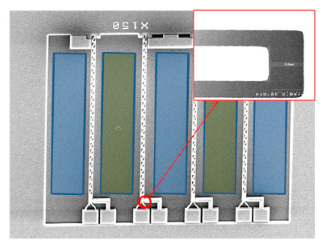
Figure 12.
Chip microphotograph of the instrumentation amplifier in CMOS 65-nm technology and 1 mm2 area.
Figure 12.
Chip microphotograph of the instrumentation amplifier in CMOS 65-nm technology and 1 mm2 area.

Figure 13.
Measurement setup of the hybrid circuit composed by the M&NEMS microphone and the ΔΣ modulator.
Figure 13.
Measurement setup of the hybrid circuit composed by the M&NEMS microphone and the ΔΣ modulator.

Figure 14.
M&NEMS microphone output versus frequency at sound source level of 94 dB in the 20 Hz–20 kHz frequency range.
Figure 14.
M&NEMS microphone output versus frequency at sound source level of 94 dB in the 20 Hz–20 kHz frequency range.

Figure 15.
Direct current (DC) consumption of the instrumentation amplifier with bias voltage.

Figure 16.
SNR of the instrumentation amplifier versus power consumption.

Figure 17.
Instrumentation amplifier equivalent-input referred noise.


Table 1.
Performances comparison of the instrumentation amplifier with the state-of-the art.
| Specifications | [18] | [19] | [20] | [21] | [22] | This Work |
|---|---|---|---|---|---|---|
| Technology, nm | 180 | 320 | 130 | 40 | 180 | 65 |
| Supply, V | 3.3 | 3.3 | 1.2 | 1.2 | 0.8 | 2.5 |
| Power, µW | 558 | 561 | 3 | 2 | 8 | 400 |
| CMRR, dB | 162 | 120 | 85 | 87 | 85 | 121 |
| PSRR, dB | 111 | 115 | - | - | 74 | 108 |
| Bandwidth, Hz | 59 k | 40 k | 5 k | 20 k | 670 | 20 k |
| Noise, nV/√Hz | 28.3 | 18 | 47 | 110 | 36 | 12 |
| NEF | 4.2 | 10.6 | 3.9 | 4.9 | 2.1 | 3.7 |
© 2020 by the authors. Licensee MDPI, Basel, Switzerland. This article is an open access article distributed under the terms and conditions of the Creative Commons Attribution (CC BY) license (http://creativecommons.org/licenses/by/4.0/).
Share and Cite
MDPI and ACS Style
Nebhen, J.; Ferreira, P.M.; Mansouri, S. A Chopper Stabilization Audio Instrumentation Amplifier for IoT Applications. J. Low Power Electron. Appl. 2020, 10, 13. https://0-doi-org.brum.beds.ac.uk/10.3390/jlpea10020013
AMA Style
Nebhen J, Ferreira PM, Mansouri S. A Chopper Stabilization Audio Instrumentation Amplifier for IoT Applications. Journal of Low Power Electronics and Applications. 2020; 10(2):13. https://0-doi-org.brum.beds.ac.uk/10.3390/jlpea10020013
Chicago/Turabian StyleNebhen, Jamel, Pietro M. Ferreira, and Sofiene Mansouri. 2020. "A Chopper Stabilization Audio Instrumentation Amplifier for IoT Applications" Journal of Low Power Electronics and Applications 10, no. 2: 13. https://0-doi-org.brum.beds.ac.uk/10.3390/jlpea10020013
Note that from the first issue of 2016, this journal uses article numbers instead of page numbers. See further details here.