Accurate Analysis and Design of Integrated Single Input Schmitt Trigger Circuits


Abstract
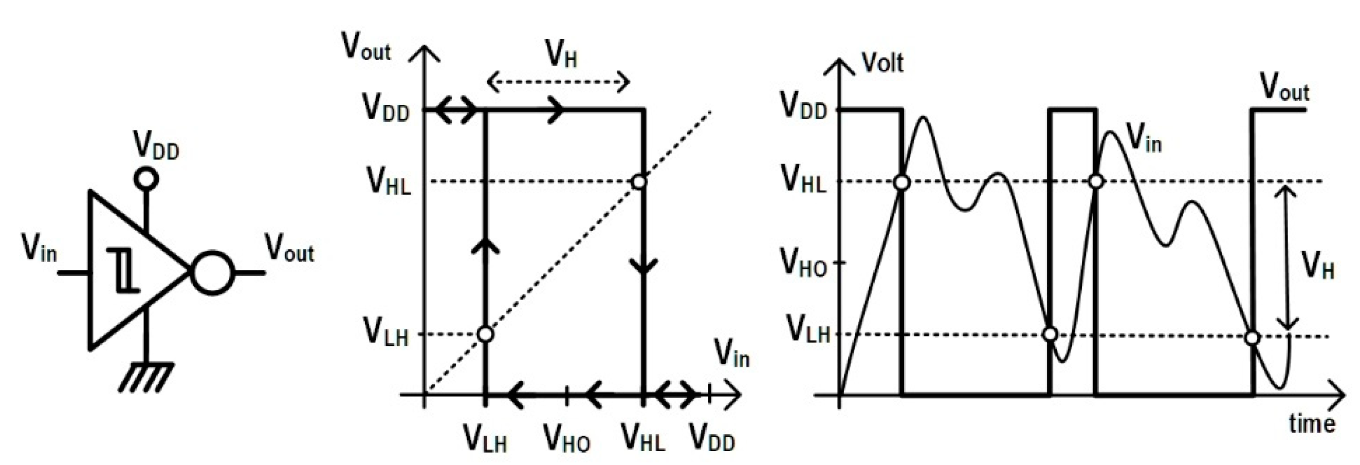
:1. Introduction
2. Analysis of Schmitt Trigger (ST) Circuits
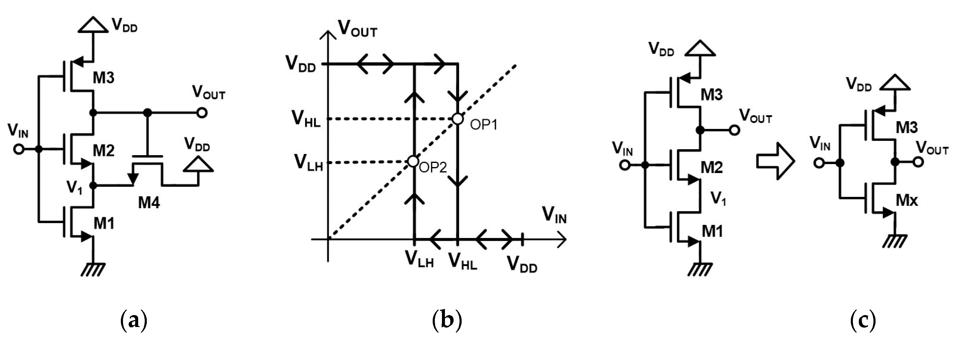
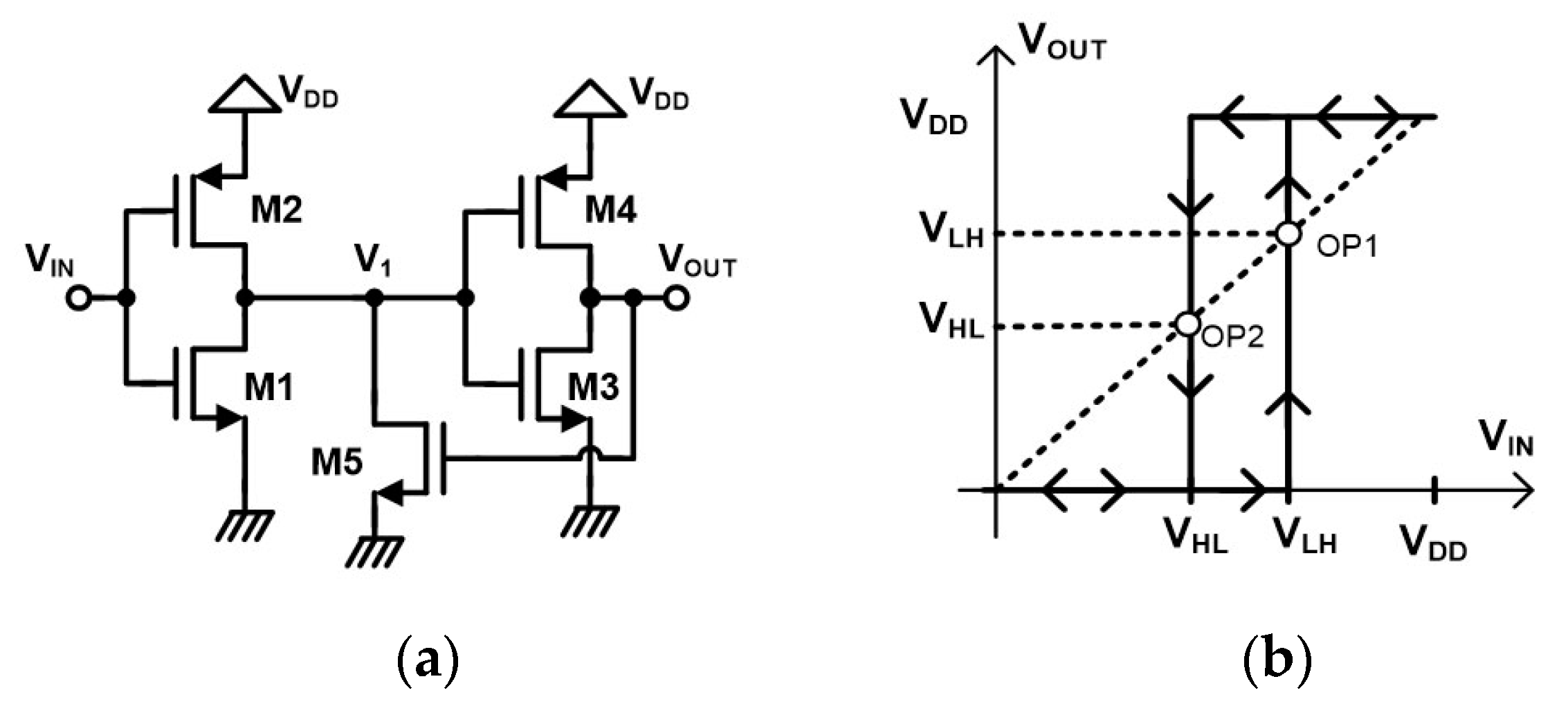
2.1. Dokic Schmitt Trigger Circuits
2.1.1. N-Type ST by Dokic
VHL Voltage
VLH Voltage
Hysteresis Voltage
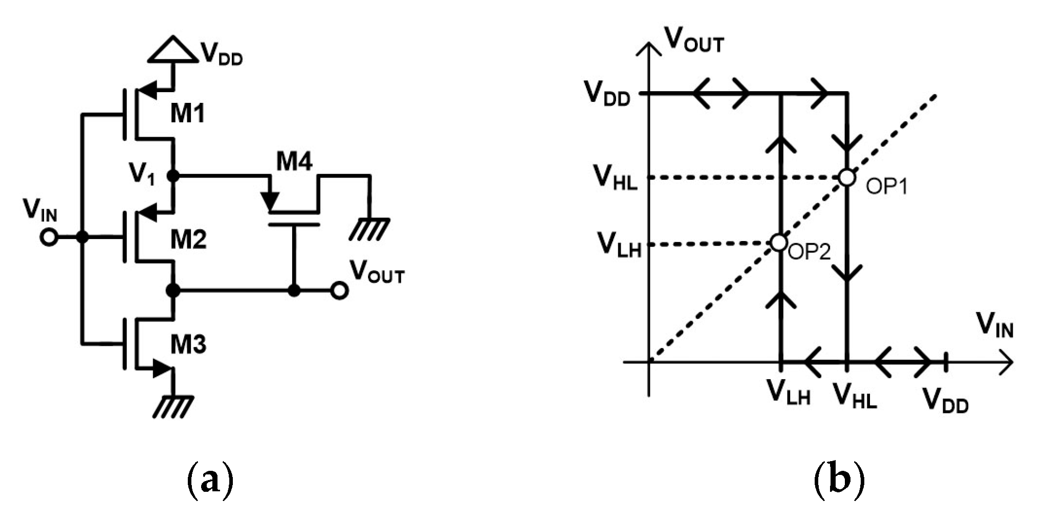
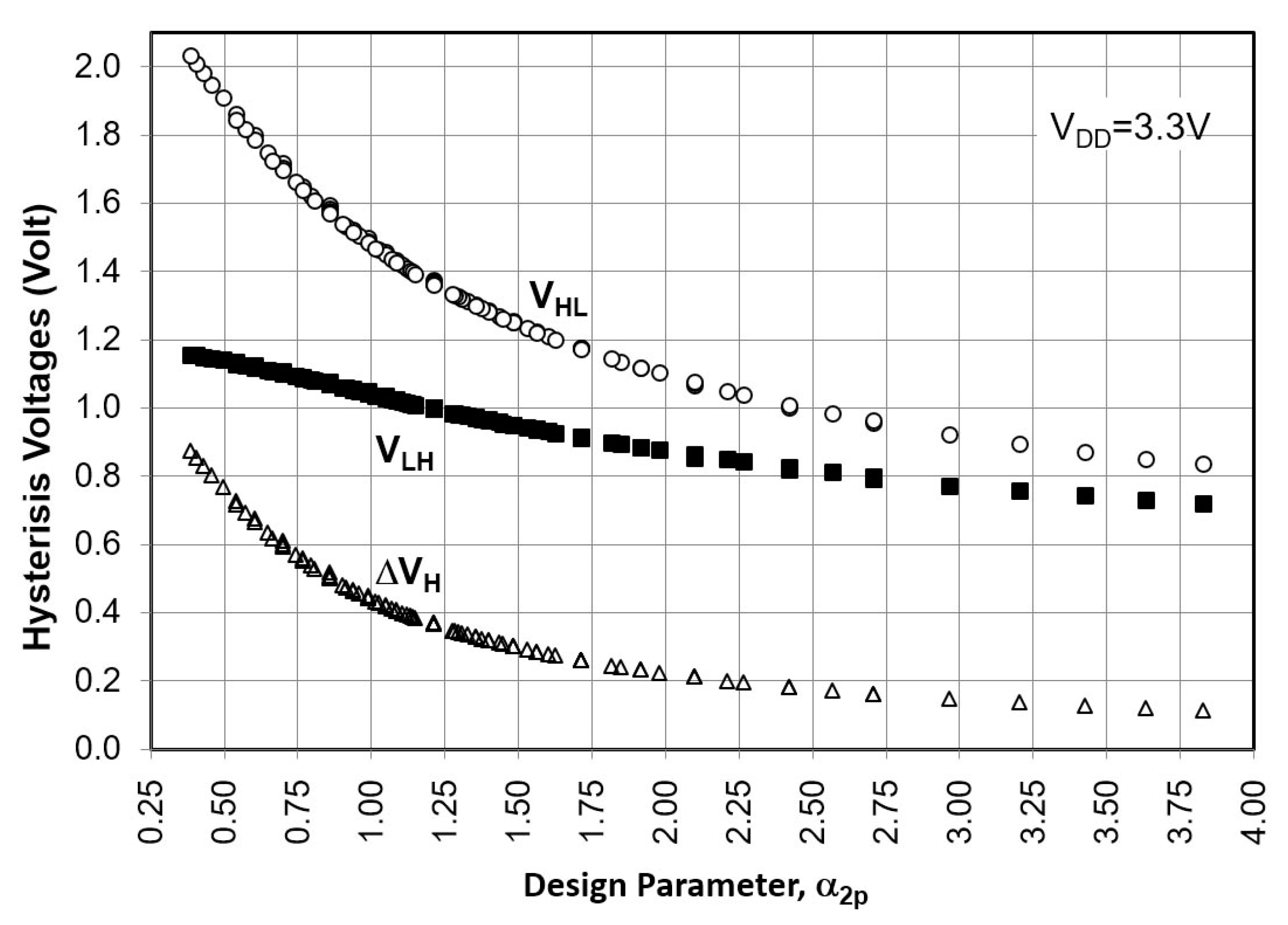
2.1.2. P-Type ST by Dokic
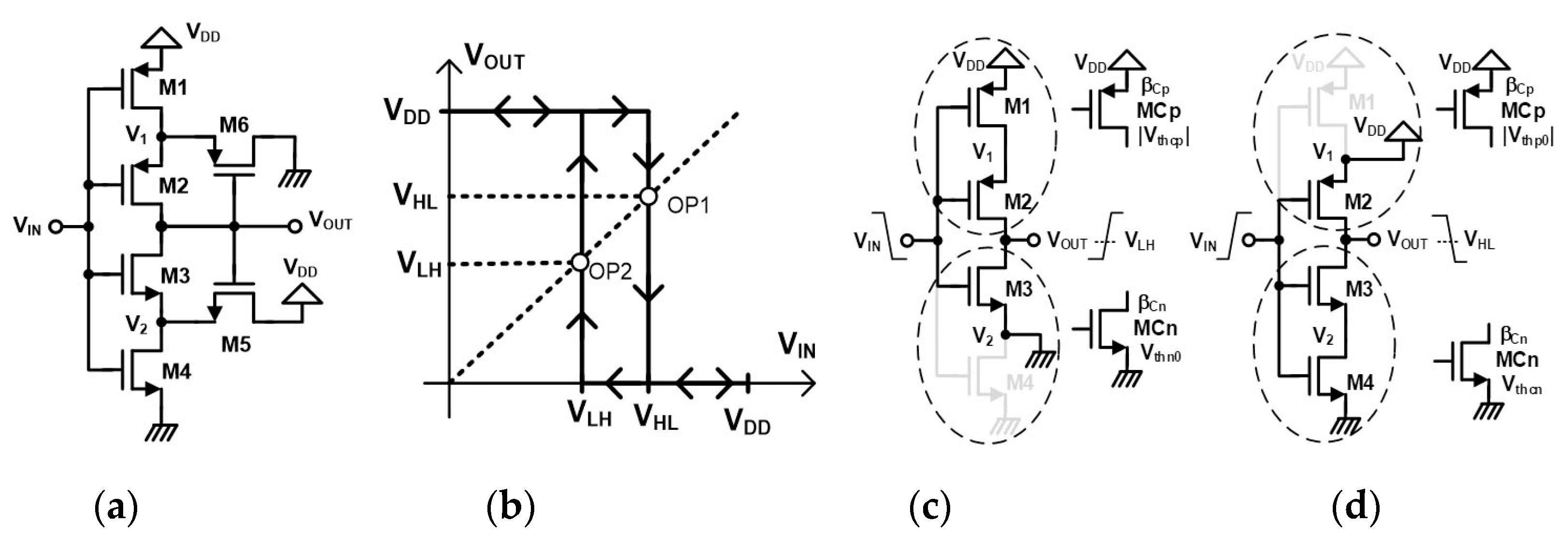
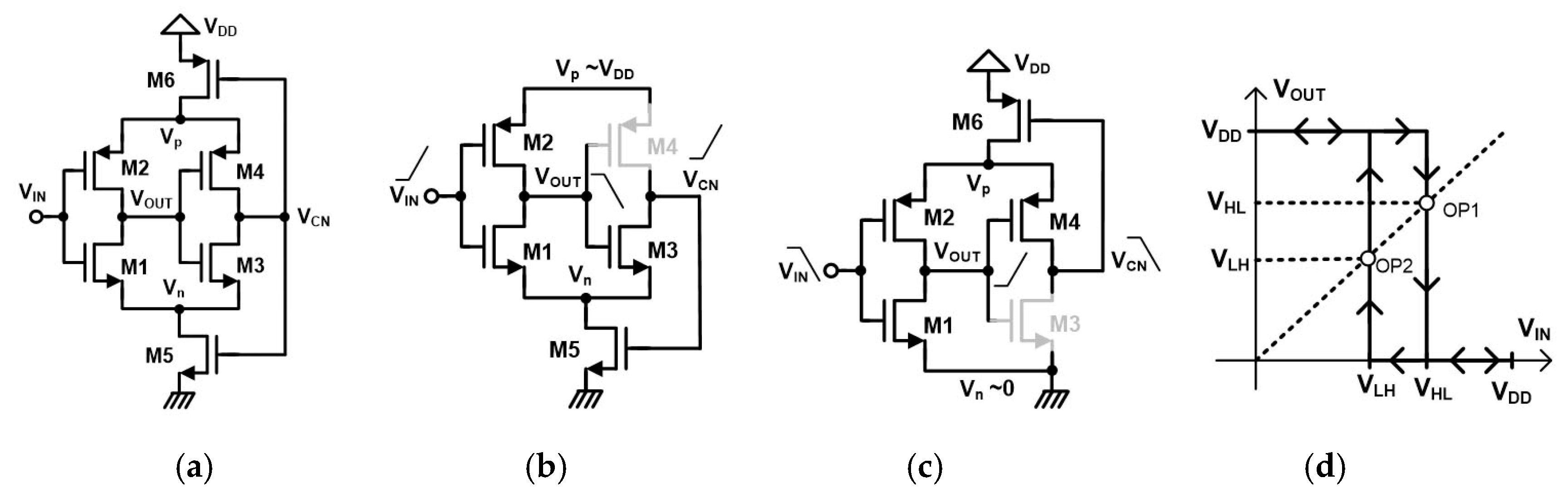
2.1.3. CMOS-Type ST by Dokic
VLH Voltage
VHL Voltage
Hysteresis Voltage
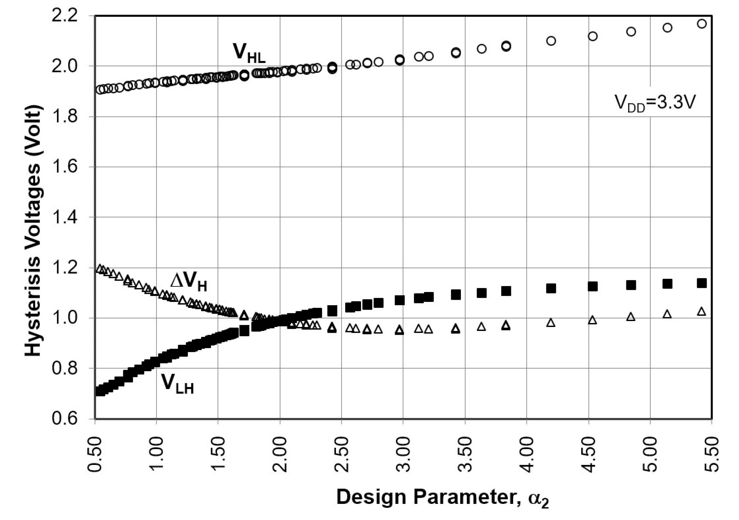
2.2. CMOS-Type Schmitt Trigger by Steyaert
2.2.1. VLH Voltage
2.2.2. VHL Voltage
2.2.3. Hysteresis Voltage
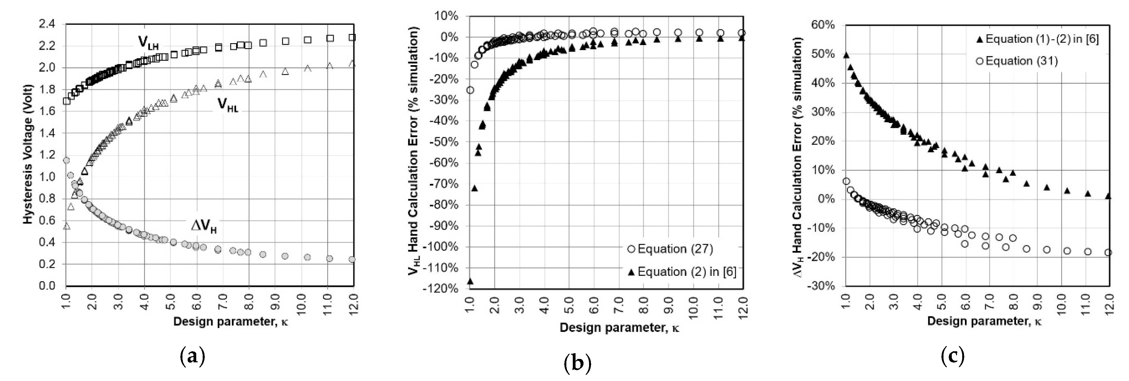
2.3. Non-Inverting Schmitt Trigger by Pedroni
Hysteresis Voltages
2.4. Low-Power CMOS-Type Schmitt Trigger by Al-Sarawi
2.4.1. VHL Voltage
2.4.2. VLH Voltage
2.4.3. Hysteresis Voltages
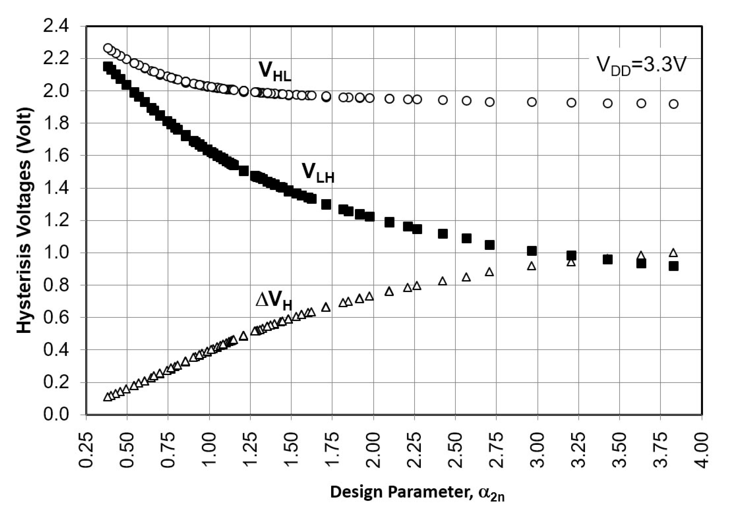
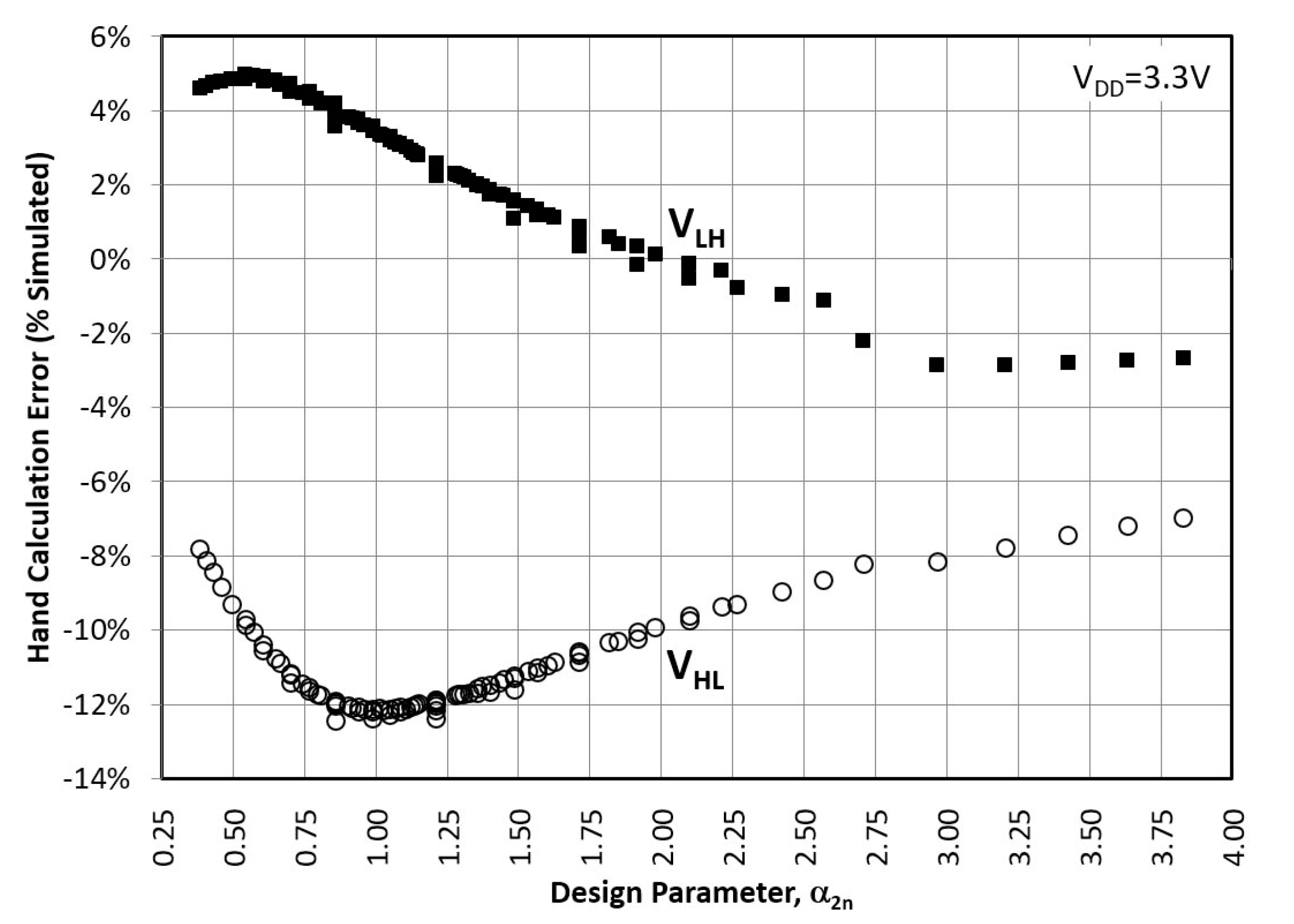
3. Comparison of Simulation and Hand Calculations
3.1. Dokic ST Circuits
3.1.1. N-Type ST by Dokic
3.1.2. P-Type ST by Dokic
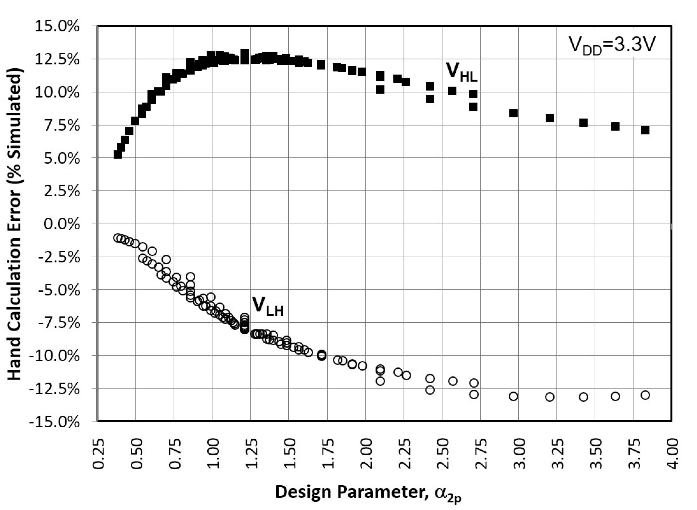
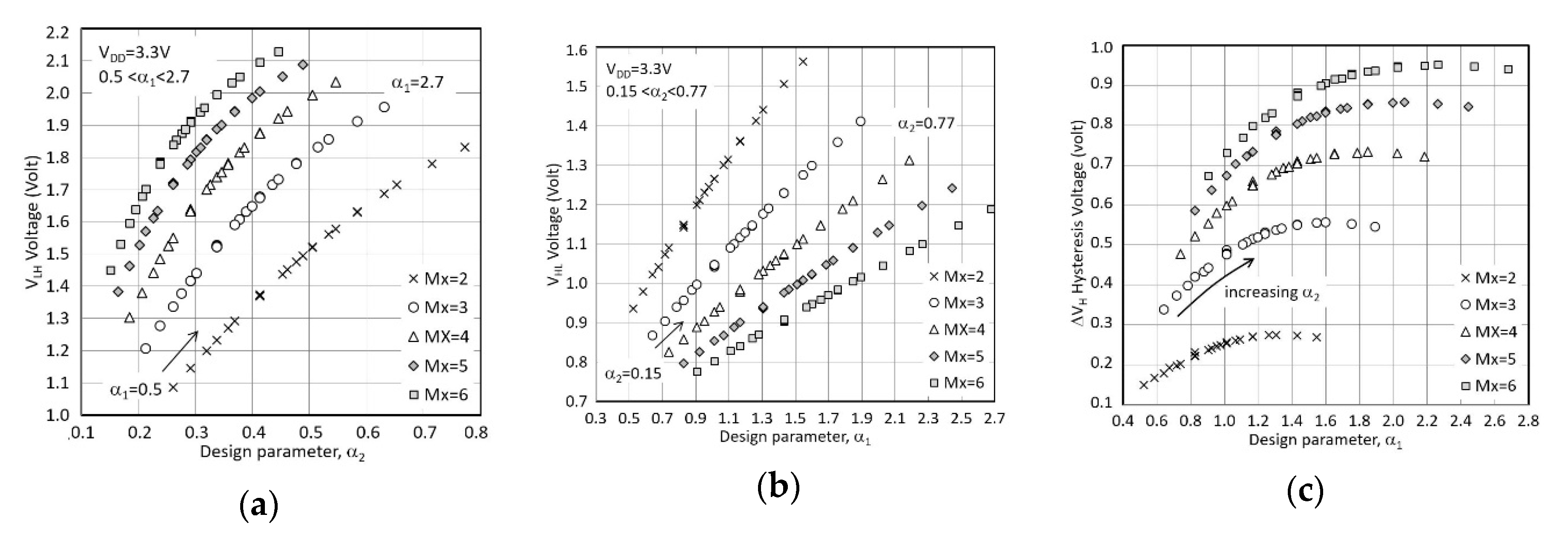
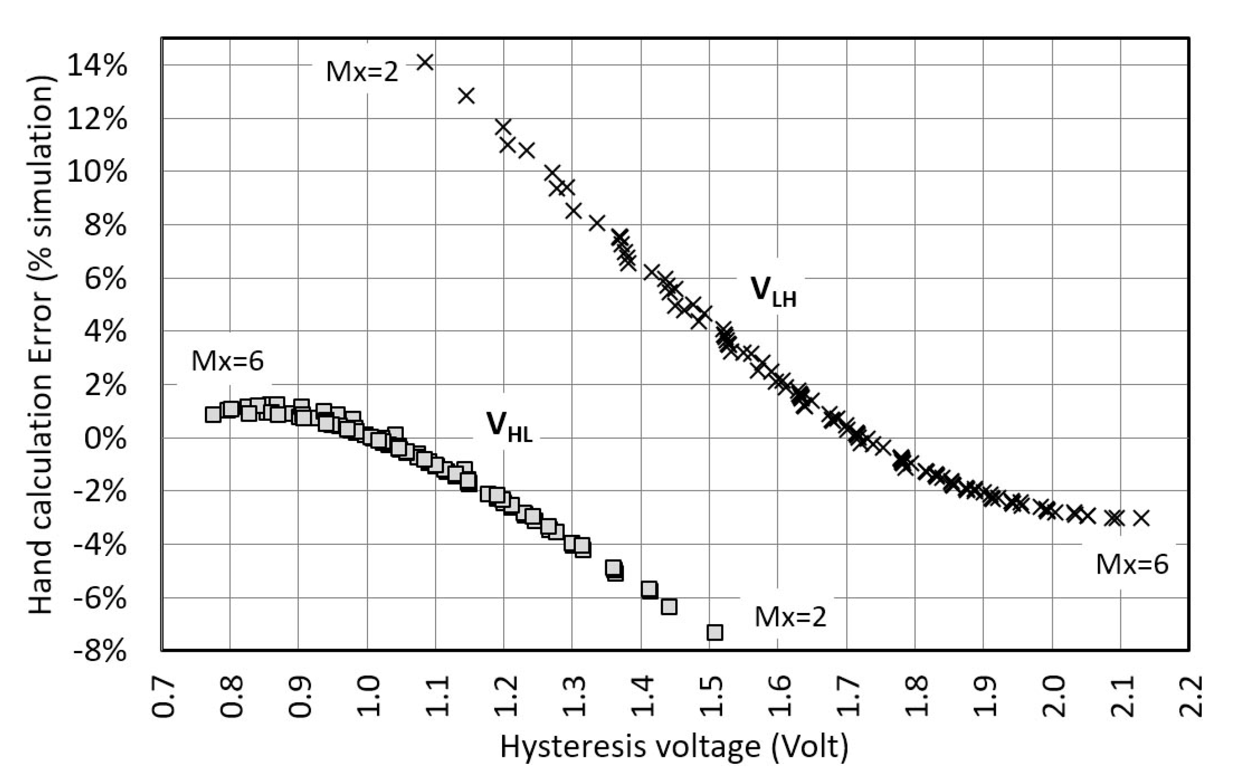
3.1.3. CMOS-Type ST by Dokic
3.2. CMOS-Type ST by Steyaert
3.3. Non-Inverting ST by Pedroni
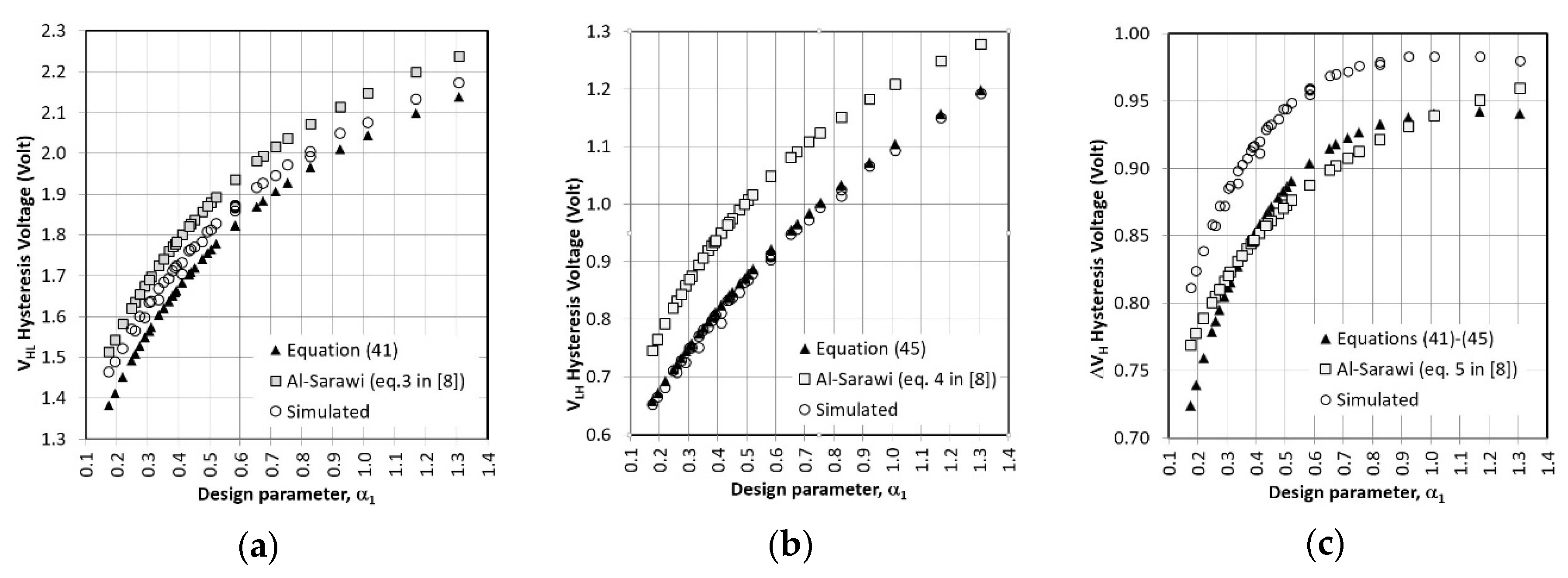
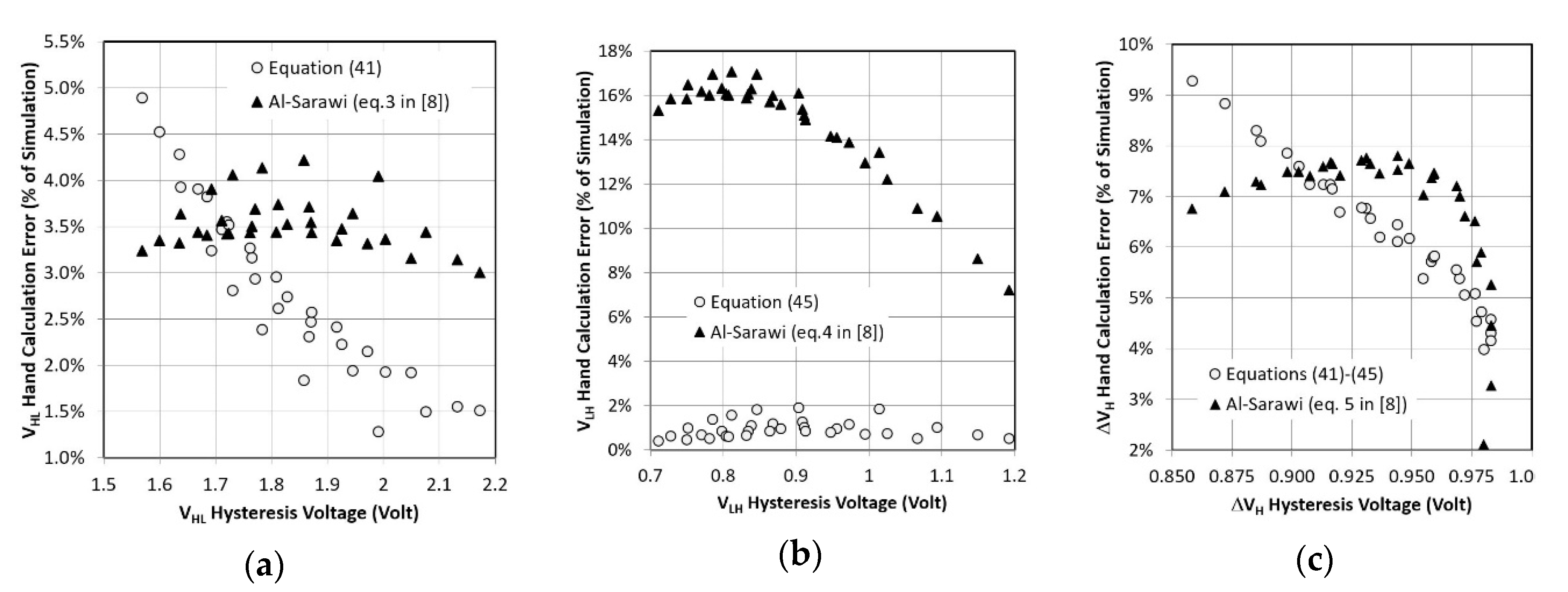
3.4. CMOS-Type ST by Al-Sarawi
3.5. Comparison of All Circuits
4. Conclusions
Author Contributions
Funding
Conflicts of Interest
References
- Wang, L.; Ross, J. Synchronous neural networks of nonlinear threshold elements with hysteresis. Proc. Natl. Acad. Sci. USA 1990, 87, 988–992. [Google Scholar] [CrossRef] [PubMed] [Green Version]
- Wang, L. Suppressing chaos with hysteresis in a higher order neural network. IEEE Trans. Circuits Syst. II Analog. Digit. Signal. Process. 1996, 43, 845–846. [Google Scholar] [CrossRef]
- Takefuji, Y.; Lee, K.C. An artificial hysteresis binary neuron: A model suppressing the oscillatory behaviors of neural dynamics. Biol. Cybern. 1991, 64, 353–356. [Google Scholar] [CrossRef]
- Merolla, P.A.; Arthur, J.V.; Alvarez-Icaza, R.; Cassidy, A.S.; Sawada, J.; Akopyan, F.; Jackson, L.; Imam, N.; Guo, C.; Nakamura, Y.; et al. A million spiking-neuron integrated circuit with a scalable communication network and interface. Science 2014, 345, 668–673. [Google Scholar] [CrossRef]
- Dokic, B.L. CMOS Schmitt triggers. IEE Proc. G Electron. Circuits Syst. 1984, 131, 197–202. [Google Scholar] [CrossRef]
- Steyaert, M.; Sansen, W. Novel CMOS Schmitt trigger. Electron. Lett. 1986, 22, 203–204. [Google Scholar] [CrossRef]
- Pedroni, V.A. Low-voltage high-speed Schmitt trigger and compact window comparator. Electron. Lett. 2005, 41, 1213–1214. [Google Scholar] [CrossRef] [Green Version]
- Al-Sarawi, S.F. Low power Schmitt trigger circuit. Electron. Lett. 2002, 38, 1009–1010. [Google Scholar] [CrossRef]
- McGrail, J.M. CMOS Schmitt trigger. US Patent US4703201, 14 August 1987. [Google Scholar]
- Allstot, D.J. A precision variable-supply CMOS comparator. IEEE J. Solid State Circuits. 1982, 17, 1080–1087. [Google Scholar] [CrossRef]
- Wang, Z. CMOS adjustable Schmitt triggers. IEEE Trans. Instrum. Meas. 1991, 40, 601–605. [Google Scholar] [CrossRef]
- Yuan, F.; Soltani, N. Low-voltage low VDD sensitivity relaxation oscillator for passive wireless microsystems. Electron. Lett. 2009, 45, 1057–1058. [Google Scholar] [CrossRef]
- Lee, W.F.; Chan, P.K. A low-cost programmable clock generator for switched-capacitor circuit applications. Analog Integr. Circuits Signal Process. 2006, 47, 247–257. [Google Scholar] [CrossRef]
- Garimella, A.; Kalyani-Garimella, L.M.; Ramírez-Angulo, J.; Lopez-Martin, A.J. Versatile multi-decade CMOS voltage-controlled oscillator with accurate amplitude and pulse width control. Analog Integr. Circuits Signal Process. 2009, 60, 83–92. [Google Scholar] [CrossRef]
- Unterassinger, H.; Flatscher, M.; Herndl, T.; Jongsma, J.; Pribyl, W. Design of a digitally controlled oscillator for a Delta-Sigma phase-locked loop in a 0.13 μm CMOS-process. E Elektrotechnik Inf. Tech. 2010, 127, 86–90. [Google Scholar] [CrossRef]
- Chen, S.L.; Ker, M.D. A new Schmitt trigger circuit in a 0.13 μm 1/2.5 V CMOS process to receive 3.3 V input signals. In Proceedings of the 2004 International Symposium on Circuits and Systems, Vancouver, BC, Canada, 23–26 May 2004; pp. 573–576. [Google Scholar]
- Chen, S.L.; Ker, M.D. A new Schmitt trigger circuit in a 0.13-/spl mu/m 1/2.5-V CMOS process to receive 3.3-V input signals. IEEE Trans. Circuits Syst. II Express Briefs. 2005, 52, 361–365. [Google Scholar] [CrossRef]
- Morimura, H.; Shimannura, T.; Fujii, K.; Shigematsu, S.; Okazaki, Y.; Katsuyuki, M. A zero-sink-current Schmitt trigger and window-flexible counting circuit for fingerprint sensor/identifier. In Proceedings of the Solid-State Circuits Conference, San Francisco, CA, USA, 15–19 February 2004; pp. 122–517. [Google Scholar]
- Park, D.; Rhee, J.; Joo, Y. Wide dynamic range and high SNR self-reset CMOS image sensor using a Schmitt trigger. In Proceedings of the IEEE Sensors Conference, Lecce, Italy, 26–29 October 2008; pp. 294–296. [Google Scholar]
- Park, D.; Joo, Y.; Koppa, S. A simple and robust self-reset CMOS image sensor. In Proceedings of the 53rd IEEE International Midwest Symposium on Circuits and Systems, Seattle, WA, USA, 1–4 August 2010; pp. 680–683. [Google Scholar]
- Koppa, S.; Park, D.; Joo, Y.; Jung, S. A 105.6dB DR and 65dB peak SNR self-reset CMOS image sensor using a Schmitt trigger circuit. In Proceedings of the IEEE 54th International Midwest Symposium on Circuits and Systems, Seoul, Korea, 7–10 August 2011; pp. 1–4. [Google Scholar]
- Sasagawa, K. An Implantable CMOS Image Sensor with Self-Reset Pixels for Functional Brain Imaging. IEEE Trans. Electron. Devices 2016, 63, 215–222. [Google Scholar] [CrossRef]
- Kagawa, K.; Yoshida, N.; Tokuda, T.; Ohta, J.; Nunoshita, M. Building a Simple Model of a Pulse-Frequency-Modulation Photosensor and Demonstration of a 128 × 128-pixel Pulse-Frequency-Modulation Image Sensor Fabricated in a Standard 0.35-$mUm Complementary Metal-Oxide Semiconductor Technology. Opt. Rev. 2004, 11, 176–181. [Google Scholar] [CrossRef]
- Sun, K.; Yuan, X.; Meng, L.; Rao, C. An ultra-low power CMOS oscillating pixel array for retina implantation. Opto-Electron. Lett. 2010, 6, 275–277. [Google Scholar] [CrossRef]
- Kim, H.; Kim, H.J.; Chung, W.S. Pulse width Modulation Circuits Using CMOS OTAs. IEEE Trans. Circuits Syst. 2007, 54, 1869–1878. [Google Scholar] [CrossRef]
- Kulkarni, J.P.; Kim, K.; Roy, K. A 160 mV Robust Schmitt Trigger Based Subthreshold SRAM. IEEE J. Solid-State Circuits. 2007, 42, 2303–2313. [Google Scholar] [CrossRef]
- Kulkarni, J.P.; Kim, K.; Roy, K. A 160 mV, fully differential, robust Schmitt trigger based sub-threshold SRAM. In Proceedings of the ACM/IEEE International Symposium on Low Power Electronics and Design, Portland, OR, USA, 27–29 August 2007; pp. 171–176. [Google Scholar]
- Kulkarni, J.P.; Roy, K. Ultralow-Voltage Process-Variation-Tolerant Schmitt-Trigger-Based SRAM Design. IEEE Trans. Very Large Scale Integr. VLSI Syst. 2012, 20, 319–332. [Google Scholar] [CrossRef]
- Roy, K.; Kulkarni, J.; Hwang, M. Low-voltage process-adaptive logic and memory arrays for ultralow-power sensor nodes. In Proceedings of the IEEE Sensors, Canterbury, New Zealand, 25–28 October 2009; pp. 185–188. [Google Scholar]
- Kim, Y.H.; Park, S.C.; Yoo, H.J. An ultra compact CMOS transceiver for HF multi-standard RFID reader. In Proceedings of the IEEE International Symposium on Radio-Frequency Integration Technology, Singapore, 9–11 December 2009; pp. 48–51. [Google Scholar]
- Myoeng-Jae, C.; Sung-Eon, J. Design of low power ASK CMOS demodulator circuit for RFID tag: Design of All-MOSFET low power ASK demodulator. In Proceedings of the IEEE International Conference of Electron Devices and Solid-State Circuits, Golden Mile, Hong Kong, China, 15–17 December 2010; pp. 1–4. [Google Scholar]
- Song, H.J.; Kim, Y.H.; Park, S.C.; Yoo, H.J. A fully integrated HF multi-standard RFID transceiver for compact mobile terminals. In Proceedings of the 2010 IEEE International Conference on RFID-Technology and Applications, Orlando, FL, USA, 14–16 June 2010; pp. 245–250. [Google Scholar]
- Beheshti, B.; Jalali, M. A low-power noncoherent BPSK demodulator for implantable medical devices. In Proceedings of the IEEE International Conference on Electronics Design, Systems and Applications, Kuala Lumpur, Malaysia, 5–6 November 2012; pp. 203–206. [Google Scholar]
- Mitwong, H.; Kasemsuwan, V. Low-voltage low-power current-mode amplitude shift keying (ASK) demodulator. In Proceedings of the IEEE International Conference on Electron Devices and Solid-State Circuit, Bangkok, Thailand, 3–5 December 2012; pp. 1–4. [Google Scholar]
- Mucha, A.; Schienle, M.; Schmitt-Landsiedel, D. Sensing cellular adhesion with a CMOS integrated impedance-to-frequency converter. In Proceedings of the IEEE Sensors Applications Symposium, San Antonio, TX, USA, 22–24 February 2011; pp. 12–17. [Google Scholar]
- Rafeeque K.P., S.; Vasudevan, V. A Built-in-Self-Test Scheme for Segmented and Binary Weighted DACs. J. Electron. Test. 2004, 20, 623–638. [Google Scholar] [CrossRef]
- Hang, G.Q.; Zhu, H.L.; Zhao, P.Y.; Zhou, X.C. Adjustable Schmitt triggers using floating-gate MOS transistors. In Proceedings of the IEEE 11th International Conference on Solid-State and Integrated Circuit Technology, Xian, China, 29 October–1 November 2012; pp. 1–3. [Google Scholar]
- Hang, G.; Wang, G.; Hu, X. The design of Neural A/D converter using neuron-MOS transistor. In Proceedings of the 8th International Conference on Natural Computation, Chongqing, China, 29–31 May 2012; pp. 485–488. [Google Scholar]
- Hang, G.; Liao, Y.; Yang, Y.; Zhang, D.; Hu, X. Neuron-MOS Based Schmitt Trigger with Controllable Hysteresis. In Proceedings of the Eighth International Conference on Computational Intelligence and Security, Guangzhou, China, 17–18 November 2012; pp. 200–203. [Google Scholar]
- Salem, J.; Ha, D.S. A robust receiver for power line communications in integrated circuits. In Proceedings of the IEEE 55th International Midwest Symposium on Circuits and Systems, Boise, ID, USA, 5–8 August 2012; pp. 254–257. [Google Scholar]
- Dokania, V.; Islam, A. Circuit-level design technique to mitigate impact of process, voltage and temperature variations in complementary metal-oxide semiconductor full adder cells. IET Circuits Devices Syst. 2015, 9, 204–212. [Google Scholar] [CrossRef]
- Beiu, V.; Ibrahim, W.; Tache, M.; Kharbash, F. When one should consider Schmitt trigger gates. In Proceedings of the IEEE 15th International Conference on Nanotechnology, Roma, Italy, 27–30 July 2015; pp. 682–685. [Google Scholar]
- Wokhlu, A.; Krishna, R.V.; Agarwal, S. A low voltage mixed signal ASIC for digital clinical thermometer. In Proceedings of the Eleventh International Conference on VLSI Design, Chennai, India, 4–7 January 1998; pp. 412–417. [Google Scholar]
- Ramfos, I.; Chatzandroulis, S. A 16-channel capacitance-to-period converter for capacitive sensor applications. Analog Integr. Circuits Signal Process. 2012, 71, 383–389. [Google Scholar] [CrossRef]
- Allen, P.E.; Holberg, D.R. CMOS Analog Circuit Design; Oxford University Press: Oxford, UK, 2002. [Google Scholar]


| Parameter | NMOS | PMOS |
|---|---|---|
| Transconductance (KP) (μA/V2) | 170 | 58 |
| Threshold Voltage (Vth0) (V) | 0.50 | −0.65 |
| ST Circuit | Trise (ns) | Tfall (ns) | Area(μm) | Power (μW) | ΔVH (V) | FoM |
|---|---|---|---|---|---|---|
| Dokic (N) [5] | 1.636 | 0.109 | 7.60 | 58.51 | 1.110 | 1.43 |
| Dokic (P) [5] | 0.412 | 1.507 | 6.86 | 61.58 | 0.855 | 1.05 |
| Dokic (CMOS) [5] | 1.239 | 0.372 | 7.80 | 75.31 | 1.015 | 1.07 |
| Steyaert [6] | 1.308 | 3.043 | 38.20 | 186.48 | 1.150 | 0.04 |
| Pedroni [7] | 0.425 | 0.338 | 13.70 | 63.20 | 0.952 | 1.44 |
| Al-Sarawi [8] | 1.320 | 1.185 | 5.40 | 43.23 | 0.983 | 1.68 |
© 2020 by the authors. Licensee MDPI, Basel, Switzerland. This article is an open access article distributed under the terms and conditions of the Creative Commons Attribution (CC BY) license (http://creativecommons.org/licenses/by/4.0/).
Share and Cite
Elmezayen, M.R.; Hu, W.; Maghraby, A.M.; Abougindia, I.T.; Ay, S.U. Accurate Analysis and Design of Integrated Single Input Schmitt Trigger Circuits. J. Low Power Electron. Appl. 2020, 10, 21. https://0-doi-org.brum.beds.ac.uk/10.3390/jlpea10030021
Elmezayen MR, Hu W, Maghraby AM, Abougindia IT, Ay SU. Accurate Analysis and Design of Integrated Single Input Schmitt Trigger Circuits. Journal of Low Power Electronics and Applications. 2020; 10(3):21. https://0-doi-org.brum.beds.ac.uk/10.3390/jlpea10030021
Chicago/Turabian StyleElmezayen, Mohamed R., Wei Hu, Amr M. Maghraby, Islam T. Abougindia, and Suat U. Ay. 2020. "Accurate Analysis and Design of Integrated Single Input Schmitt Trigger Circuits" Journal of Low Power Electronics and Applications 10, no. 3: 21. https://0-doi-org.brum.beds.ac.uk/10.3390/jlpea10030021