An Approach for a Wide Dynamic Range Low-Noise Current Readout Circuit


Department of Electrical and Computer Engineering, Tufts University, 161 College Ave, Medford, MA 02155, USA
*
Author to whom correspondence should be addressed.
J. Low Power Electron. Appl. 2020, 10(3), 23; https://0-doi-org.brum.beds.ac.uk/10.3390/jlpea10030023
Submission received: 14 May 2020
/
Revised: 19 July 2020
/
Accepted: 27 July 2020
/
Published: 29 July 2020
Abstract
:Designing low-noise current readout circuits at high speed is challenging. There is a need for preamplification stages to amplify weak input currents before being processed by conventional integrator based readout. However, the high current gain preamplification stage usually limits the dynamic range. This article presents a 140 dB input dynamic range low-noise current readout circuit with a noise floor of 10 . The architecture uses a programmable bidirectional input current gain stage followed by an integrator-based analog-to-pulse conversion stage. The programmable current gains setting enables one to achieve higher overall input dynamic range. The readout circuit is designed and in 0.18 m CMOS and consumes 10.3 mW power from a 1.8 V supply. The circuit has been verified using post-layout simulations.
1. Introduction
There is a growing need to sense very low levels of current in many biosensors and diagnostics applications [1,2,3]. Current levels in such applications can be as low as picoamperes (pA) which are harder to detect using CMOS circuitry due to circuit noise. Several readout circuits have been developed for low current sensing. For example, an integrator or a transimpedance amplifier (TIA) has been employed to convert the current signal into a voltage signal, followed by quantization of the converted voltage signal. However, with the current in the pA range, if the integration method is adopted, it would take a long time to accumulate the small current into measurable voltage signal [4]. If a TIA is employed, the feedback resistance must be large enough (i.e., gigaohms range) to obtain high gain and there is a trade-off between achieving high dynamic range and achieving low input-referred current noise. Moreover, such a large feedback resistor cannot be reliably realized on-chip and must be externally connected. A high-value active pseudo resistor made using off-state transistors have been widely used for small current sensing [5,6,7,8]. However, the resistance is inversely proportional to the input current, which leads to a variable current gain and bandwidth applications [9].
In most applications, the small current signal needs to be amplified at high speed in bandwidths excess of 1 MHz. One such application is for nanopore sensing where the transient activity is in microseconds with Femto ampere current levels. A current conveyor is commonly employed for current amplification; however, the conventional current conveyor is not suitable for the small current amplification since the bias current of the conveyor leads to large input-referred current noise [10,11]. No-bias current conveyor has been adopted for low-noise current sensing [12]. The noise levels achieved may still be prohibitive for low current sensing. A current preamplifier was presented, featuring a matched double-MOS architecture around an amplifier to obtain current amplification in [13]. Capacitors with the same current ratio are needed to increase the bandwidth. The fixed current amplification gain leads to a smaller dynamic range. In this paper, a current preamplifier with a programmable gain is proposed to obtain bidirectional current amplification. The programmable current gains setting enables one to achieve a higher overall input dynamic range. Higher gain allows for faster operation for small input currents while lower gain avoids saturation of the integrator stage for large input currents. Thus, the variable current gain enables a wider input dynamic range. Note the input dynamic range is defined as the ratio of the largest to the smallest input signal that the circuitry can process. For a programmable gain amplifier, the dynamic range will be measured as a ratio of highest input signal level (at lowest gain setting) and the largest referred input noise ever measured for any of the gain settings. A pulse width modulation output stage provides a digital output without the need for clock. The circuit is designed in a 0.18 m CMOS process and validated using post-layout simulations.
2. Low-Noise Current Readout Architecture
2.1. Current Amplification
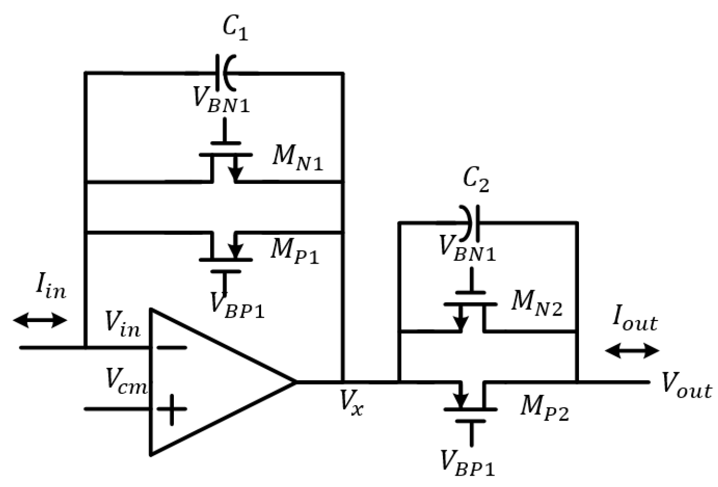
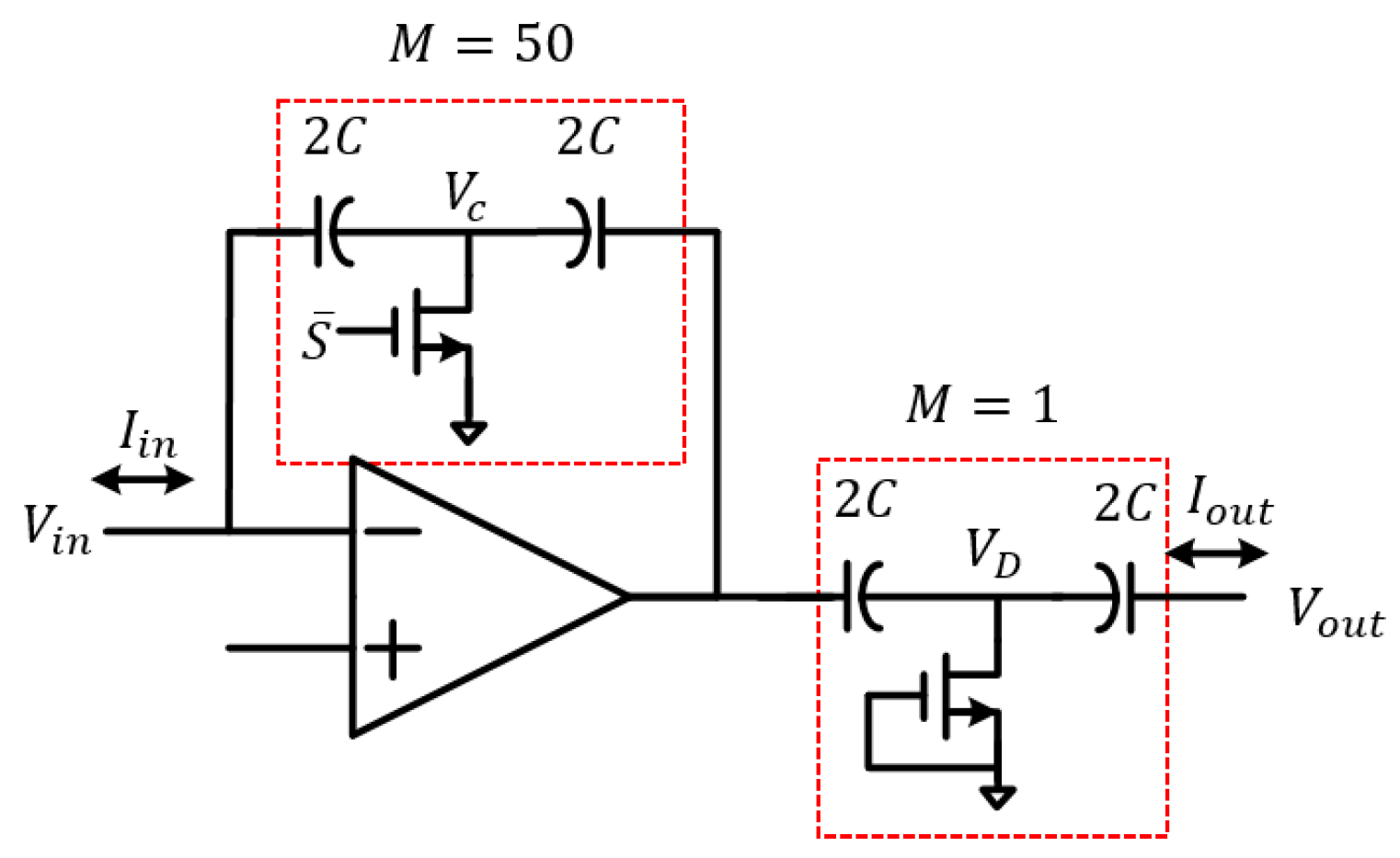
Floating current mirror is utilized to realize high current gain for amplifying weak current levels [13]. In Figure 1, transistor and are connected across the feedback loop of the amplifier. Transistor and are connected to the output node . The node connects to the negative input node of a following TIA or integrator stage which keeps at the exact same voltage potential as node or . Therefore, transistors and have the same and . The input current flows in or out through or , depending on the polarity of the current signal. Transistors and are sized N times as and , respectively. Therefore, the current through or is N times the input current signal. The capacitor and have the same ratio of N for high frequency current amplification as in Equation (1).
This architecture has the advantage that it provides high current gain so that the input-referred current noise at the input node from the following TIA or integrator is attenuated by the high current gain of this preamplification stage. However, this fixed high current gain would saturate the following TIA or integrator stage when the input current signal is large. The maximum input current is limited to the tens of nA range. In this paper, we design a programmable current preamplification stage to extend the input current signal range. This allows one to trade-off noise performance with a high dynamic range.
2.2. Programmable Gain Current Amplifier Stage
To allow processing of wide range (100 fA − 1 A) current signals, the gain of the current amplifier is designed to be programmable, and the gate control voltage of transistor and can be externally tuned to adjust to the different range of input currents. Two cascade current gain stages are implemented for a maximum of 1000×. This is designed to amplify currents as low as 100 fA. The first stage offers a maximum current gain of 50, while the second stage provides a maximum current gain of 20. The effective capacitor ratio and the effective transistor ratio are programmable to achieve different current gain for a high dynamic input current range as in Table 1.
2.3. Low-Frequency Gain Setting
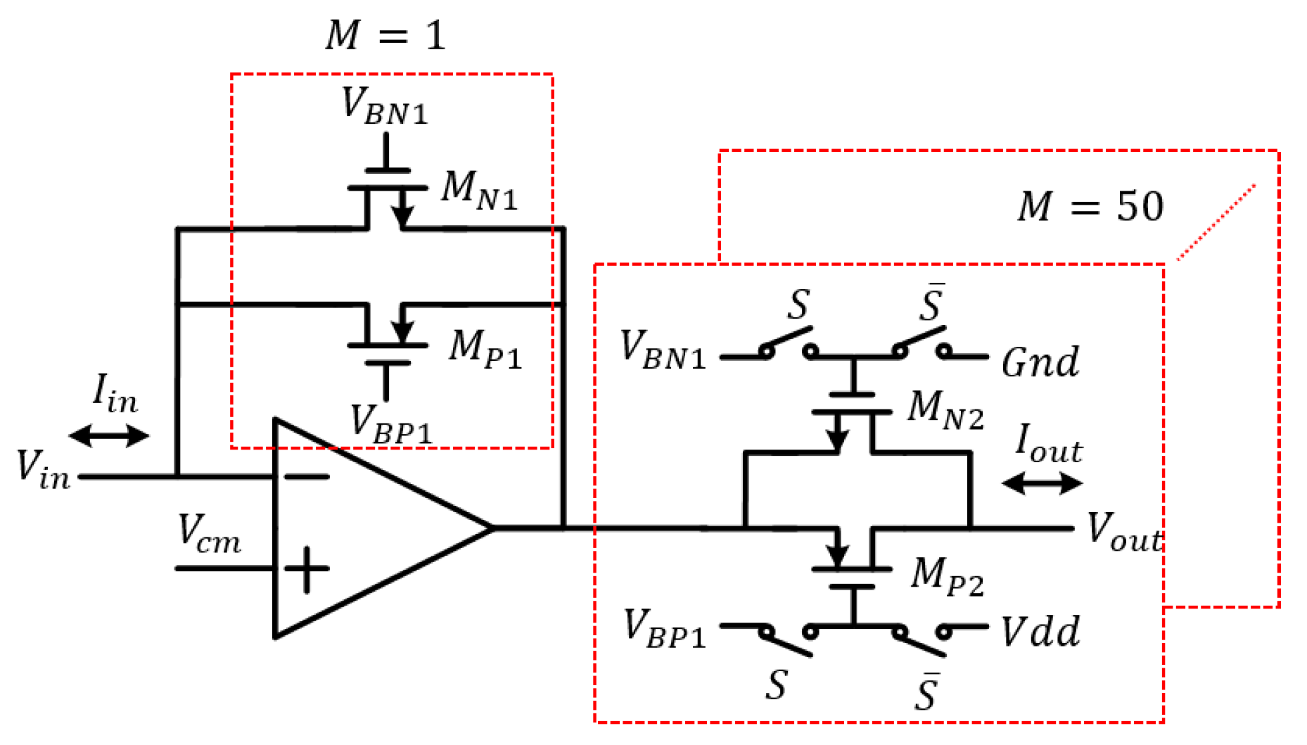
The programmable low-frequency current amplification ratio is achieved by turning on or off the mirroring transistors and in Figure 2. For the first current gain stage, there are a total of 50 sets of transistors-based current mirrors for low-frequency current signal amplification. Let us consider one example. For a gain of 10, the gates of the 10 NMOS transistors connect to , while the gates of the remaining 40 NMOS transistors connect to ; the gates of the 10 PMOS transistors connect to , while the gates of the remaining 40 PMOS transistors connect to .
2.4. High-Frequency Gain Setting
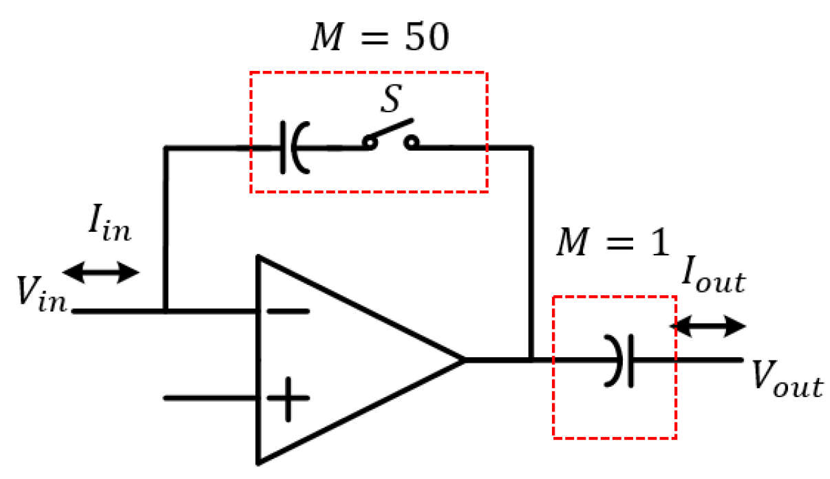
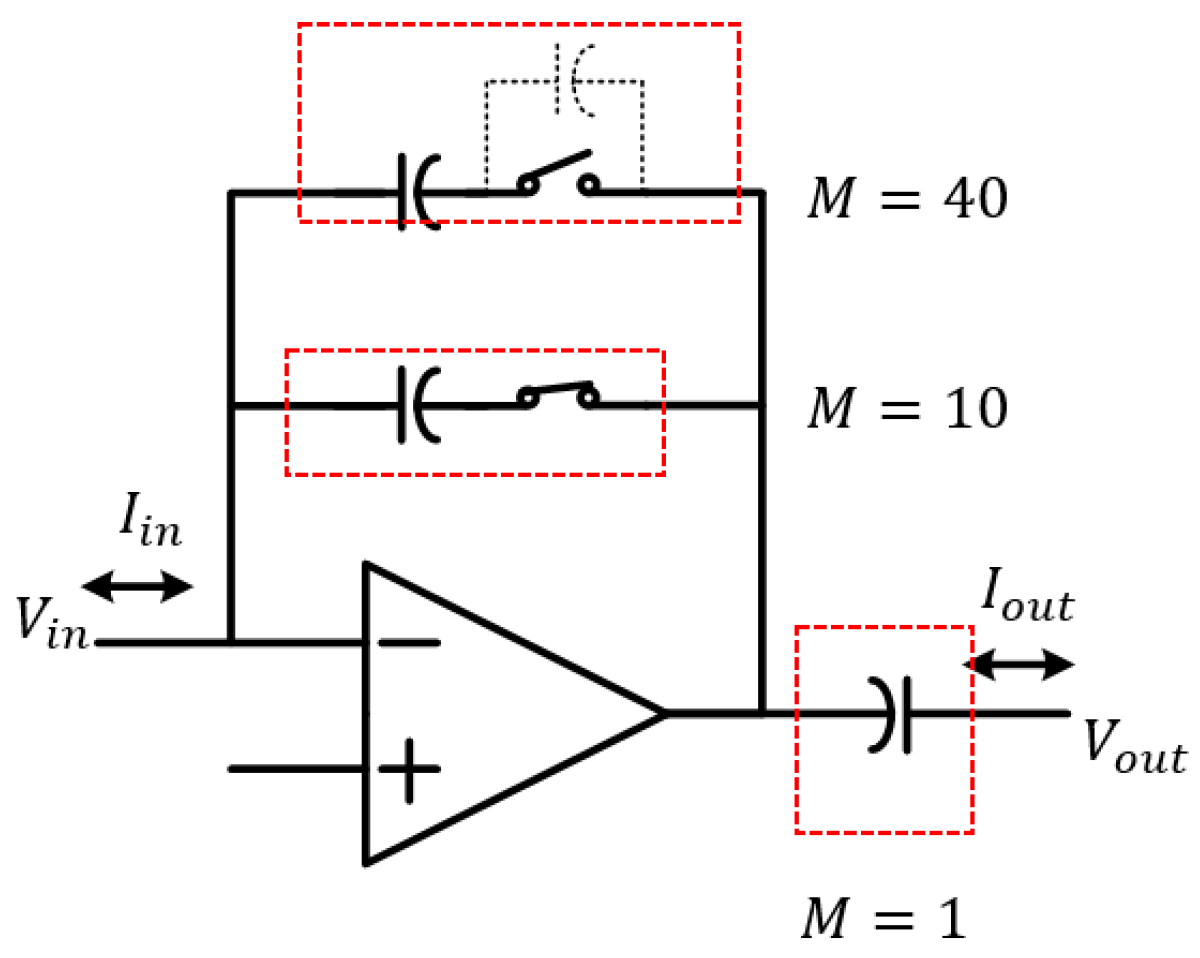
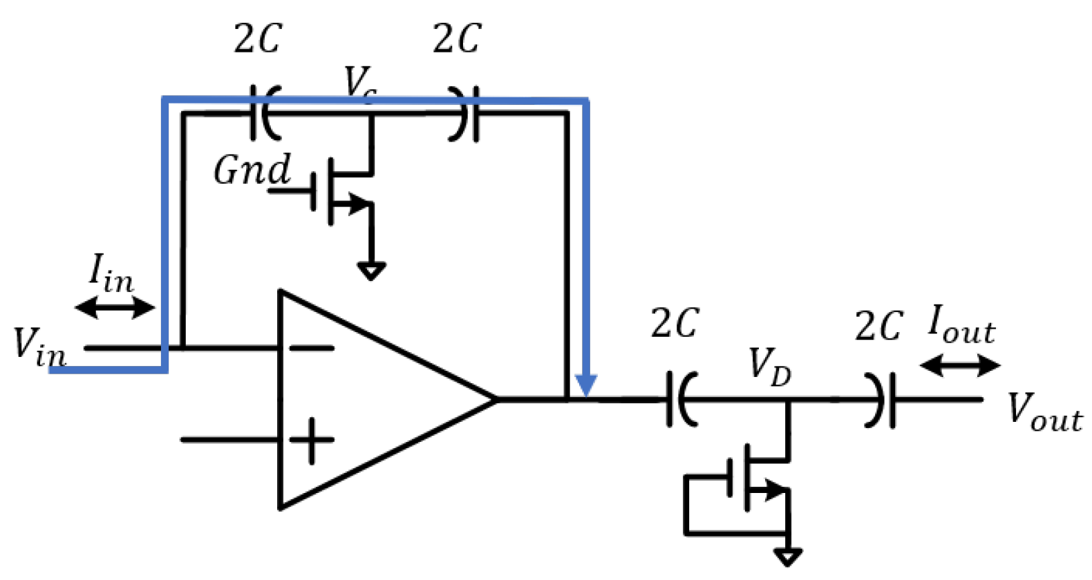
The high-frequency programmable gain is obtained by setting the feedback capacitor units. For the first current amplification stage, there are a total of 50 cells of feedback capacitors controlled by the switches in the feedback loop as in Figure 3. The switches are large to reduce the on-resistance. However, the large size switch increases the parasitic capacitance that reduces the accuracy of the high-frequency gain. For example, if a gain of 10 is selected, then the first stage enables 10 capacitors by turning on the 10 switches coupling to the capacitors. The remaining 40 switches are turned off. However, the switches from the disabled paths will still add to the parasitic capacitance in parallel with the feedback capacitors, which provide a signal path for the high-frequency signal as in Figure 4. Consequently, this will influence the gain at high frequency. The problem is exaggerated when two gain stages are cascaded.
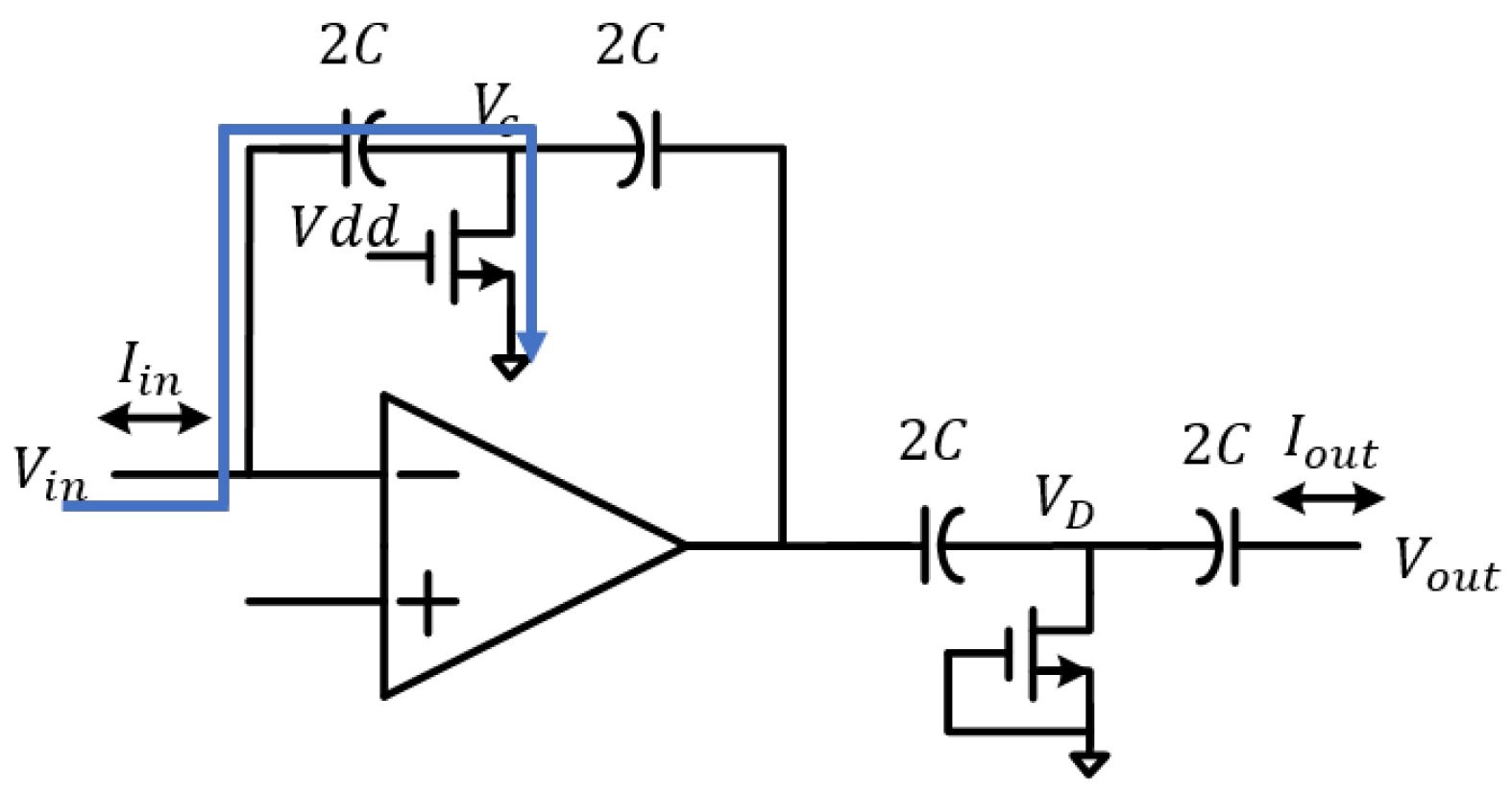
To solve this problem, we realize a T-network using two capacitors connecting in series as the feedback capacitor and move the switch between their intermediate node and ground as in Figure 5. When the feedback path is enabled, the switch is off, presenting a high impedance node at , the high-frequency signal can go through the feedback path. The two feedback capacitors connecting in series form equivalent feedback C as in Figure 6. When the feedback path is disabled, the switch is on presenting a low impedance node at , the high-frequency signal has a path to ground, without passing through the feedback path as in Figure 7. This implementation is more stable (better phase margin) compared to conventional implementation as in Figure 4. Note that the NMOS switch is not in the high-frequency signal path when the high-frequency signal gain is enabled, therefore, the size of the NMOS switch can be designed with small size introducing minimal parasitic capacitance. There is also no issue of parasitic capacitance when certain feedback paths are disabled. A dummy disabled NMOS switch is connected at node for matching. The programmable low-frequency and high-frequency current gain provide an accurate amplification over a large input current dynamic range and over a large bandwidth.
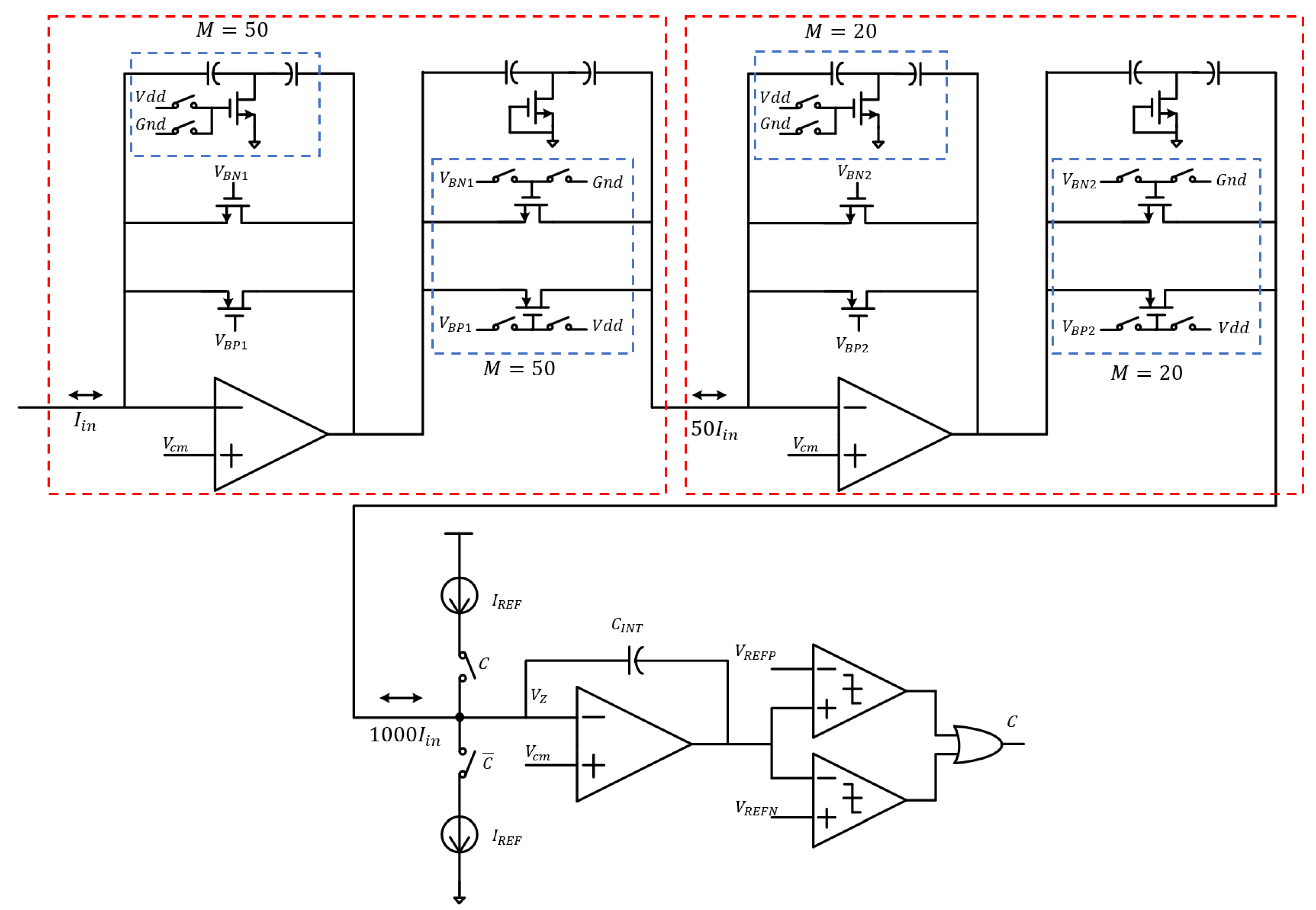
2.5. System Architecture
The readout system is composed of two current amplification stages, an integrator stage, and a pulse width modulation stage as shown in Figure 8. Two current amplification stages are cascaded to reduce the number of current mirrors. The amplified current flows into a first-order clock-less sigma-delta modulator. This works similarly to the self-resetting integrator stage that generates an output pulse width and frequency-dependent on the value of the input current [14]. If the control bit C is 1, then the current reference at the upper side is on, and the current reference at the lower side is off. The total current flowing into the integrator is . If the control bit C is 0, then the current reference at the upper side is off, and the current reference at the lower side is on. The total current flowing into the integrator is . The voltage at the output node of the integrator compares with the reference voltage and . Once crosses the voltage window(), the control bit signal C changes its polarity, which alters the direction of the reference current.
From Equations (2)–(4), utilizing charge conservation, one can show that the input current can be obtained from the pulse width of the control signal C.
The programmable low-frequency current amplification ratio is achieved by turning on or off the mirroring transistors and . For the first current gain stage, there are a total of 50 sets of the transistors-based current mirrors for low-frequency current signal amplification and 50 sets of capacitors for high-frequency current signal amplification, respectively as in Figure 8. When the gain of 10 of the first stage is selected, for example, the gates of the 10 NMOS transistors connect to , while the gates of the remaining 40 NMOS transistors connect to ; the gates of the 10 PMOS transistors connect to , while the gates of the remaining 40 PMOS transistors connect to . For the high-frequency gain, 10 sets of NMOS switches of the capacitor in the red box connect to , and the remaining 40 sets of the NMOS switches of the capacitor connected to .
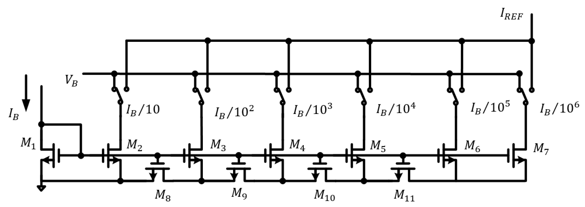
2.6. Programmable Reference Current Stage
To allow for a wide dynamic range at the input, the reference current feeds the clockless delta-sigma modulator (aka pulse width modulation stage). The reference current stage provides a selection of reference currents to the wide range input current signal. The tiny reference current is obtained by the current splitter architecture as in Figure 9 [15]. The attenuation gain is 10 in this design. The R2R topology provides the same voltage, so the current flowing in or out of this circuit will be linearly divided into two parts, according to the transistor size. Different scaled currents can be obtained from different transistor size ratios as in Table 2.
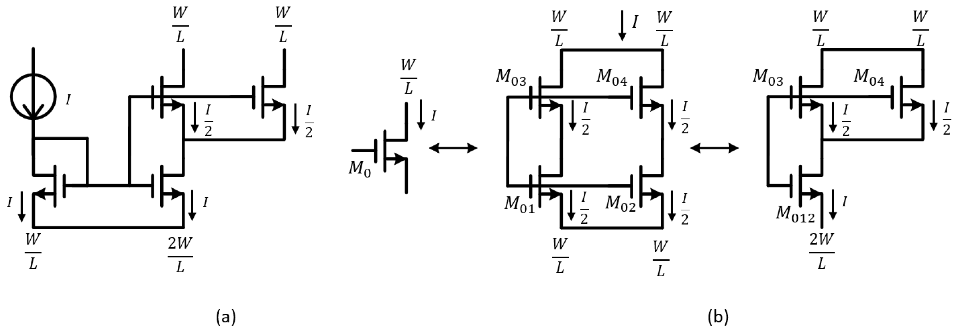
We use a simple divide-by-2 circuit to explain the operation of this circuit as in Figure 10. For a long-channel transistor, the drain current is proportional to the channel size . Based on this statement, in Figure 10a, the transistor with size is equivalent to the four identical transistors , , , and , with same size in a series-parallel configuration. The current I splits equally through each of the four transistors. Transistor and can be simplified as an equivalent transistor with a size of . Therefore, in Figure 10b, the transistor-based current split architecture by a factor of 2 is shown.
2.7. Amplifier
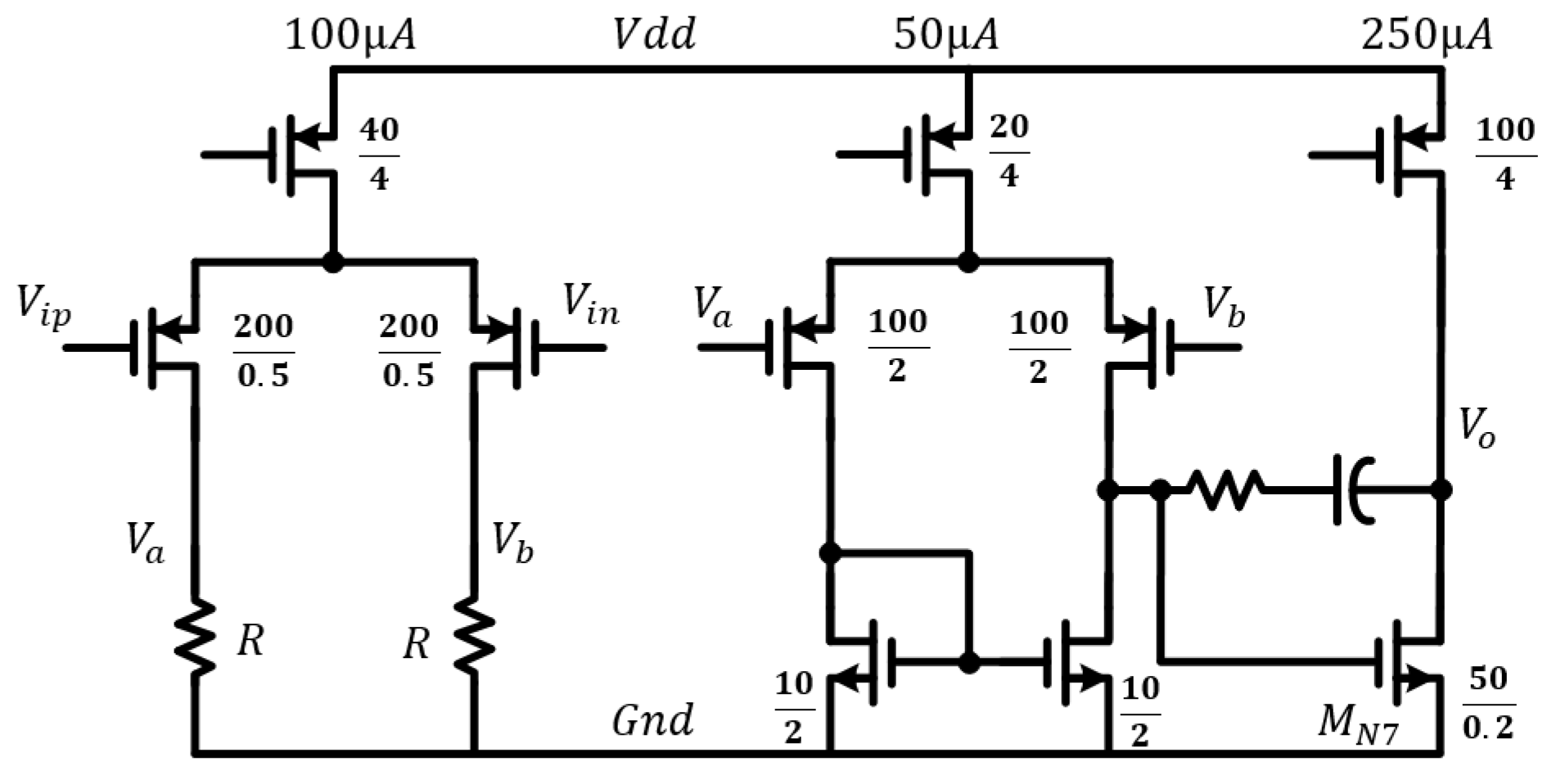
The low-noise amplifier composes of a low gain pre-amplification stage and a miller compensation amplifier stage as in Figure 11. The pre-amplification stage provides a gain of 4 with 13 MHz 3-dB bandwidth to reduce the noise and offset from the subsequent stage. The open-loop DC gain is 95 dB, unity gain bandwidth is 47 MHz, and the phase margin is 74.
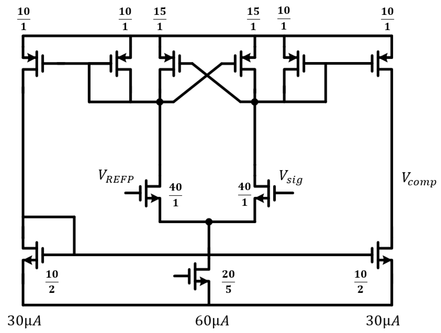
2.8. Comparator
2.9. Layout
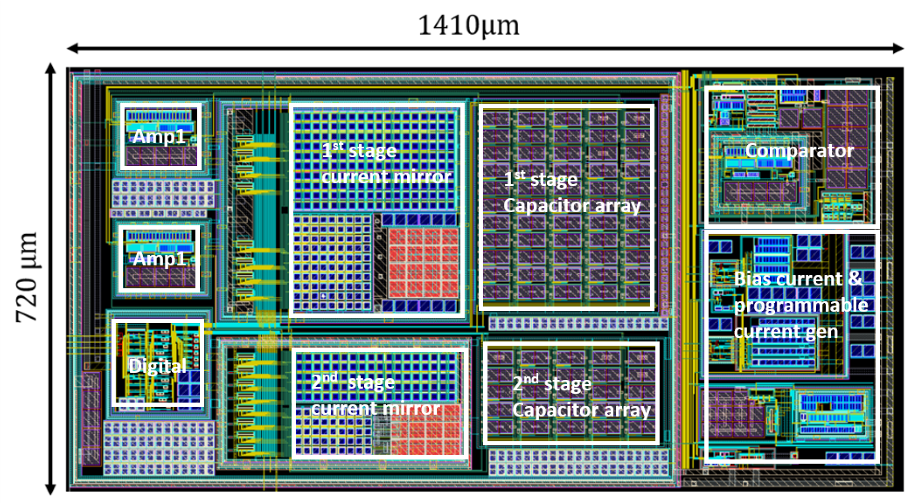
The entire design is implemented in 0.18 m CMOS technology, and the total layout area is 1410 m × 720 m. The transistors and the capacitors of the current amplification stage consume most of the layout area in Figure 13.
3. Simulation Result
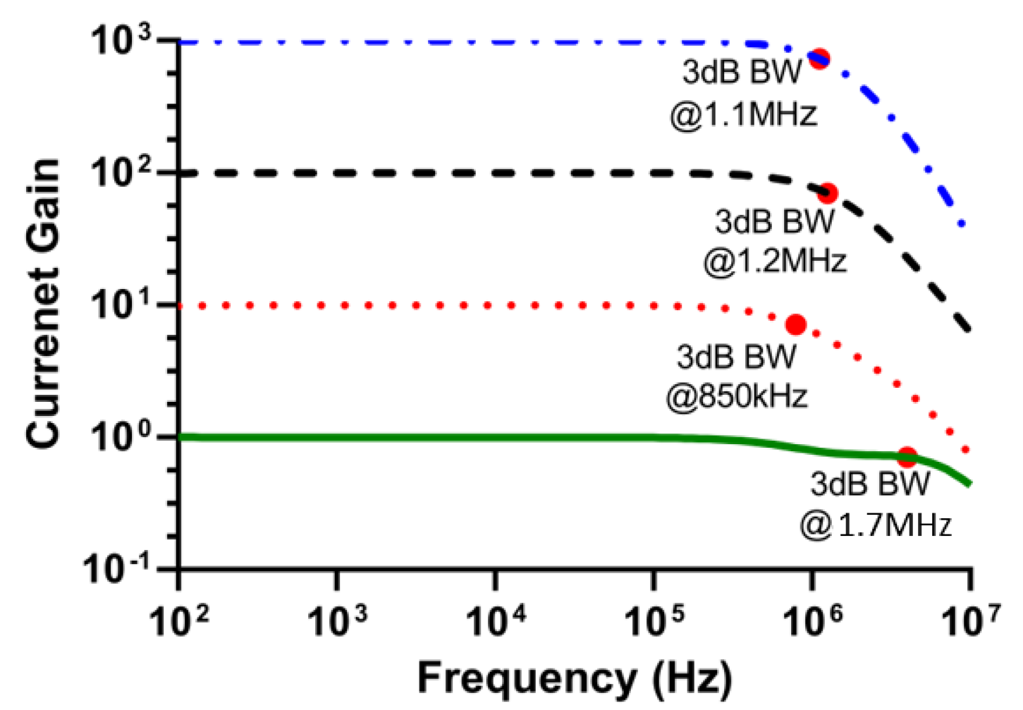
The circuit was simulated with post-layout extraction. This captures the RC parasitic effects in addition to any coupling capacitance. The current gain for wide dynamic range input current and the noise performance are simulated. By controlling the digital codes, the current gain can be programmed to be 1000×, 100×, 10×, and 1× as in Figure 14. The proposed switch connections enable the flat current gain in various current gain settings.
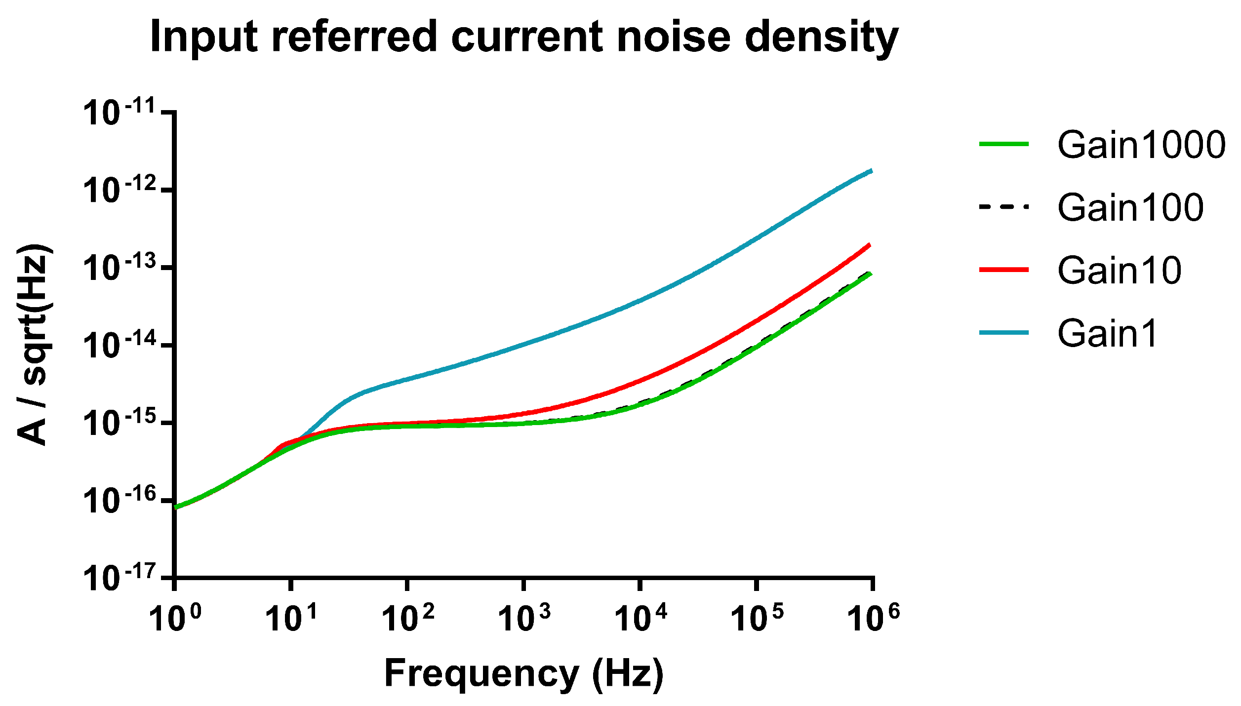
With high current pre-amplification, the input-referred current noise at the input is given by Equation (5). Note that the noise from the integration stage has been attenuated by the current-amplification gain. The feedback transistors and the input stage amplifier dominate the input reference current noise contribution. is the shot noise from in Figure 8 operating in the subthreshold region. The voltage noise from the op-amp over the input capacitance sets the minimal noise of the circuit when the input current is small.
The equivalent input voltage noise from the front-end amplifier is shown in Equation (6). The pre-amplification stage from Figure 10 has a dominant noise contribution. k is Boltzmann constant, and K is a process related constant which influences the flicker noise.
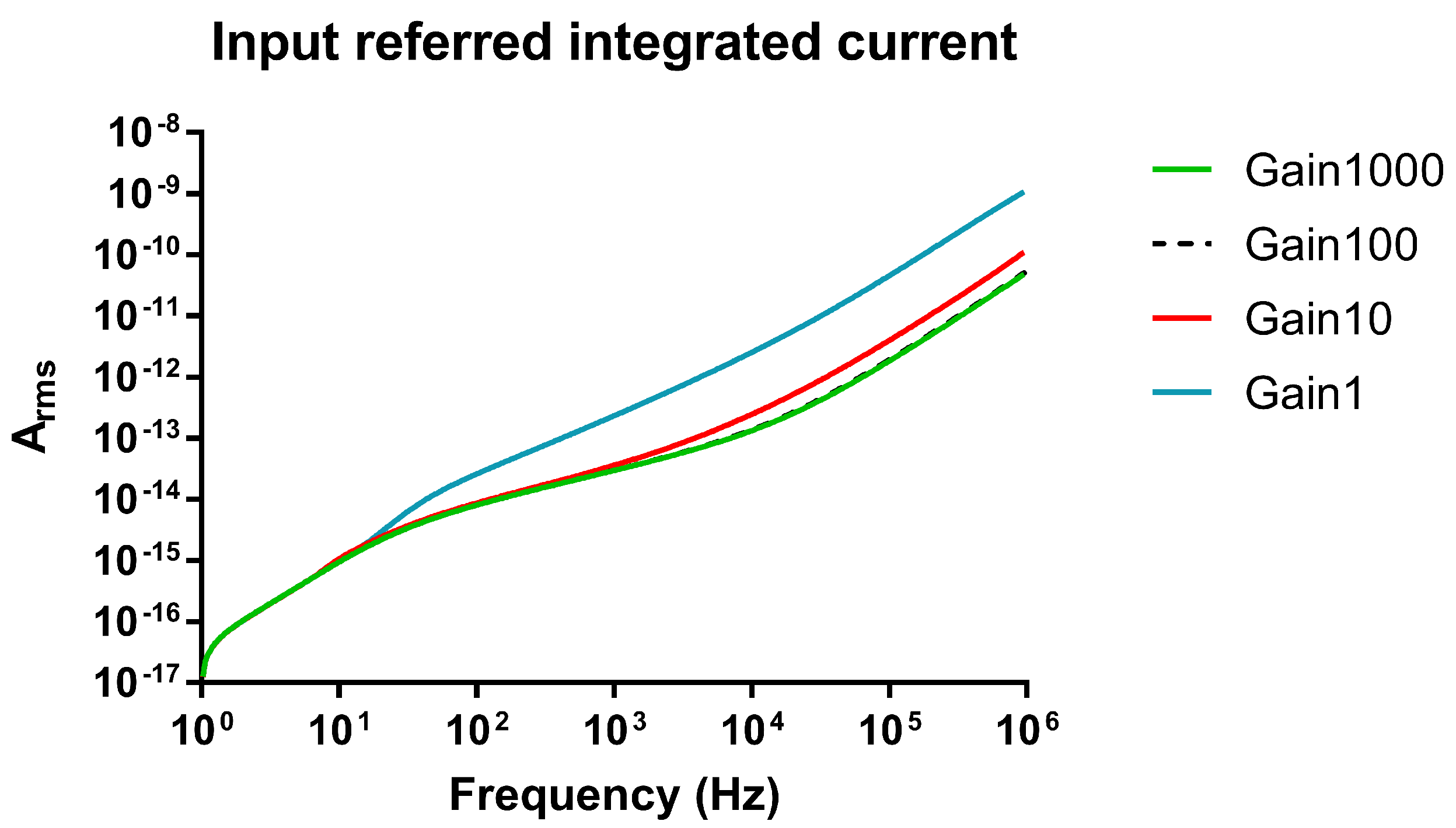
The noise density and integrated noise simulation are shown in Figure 15 and Figure 16, respectively.
Table 3 lists the integrated noise (rms) with the signal bandwidth of 100 Hz, 10 KHz, and 1 MHz, and with the current gain of 1000×, 100×, 10×, and 1×, respectively. One can choose a fast operation mode for the small input current with some trade-off with the bandwidth, or one can process high bandwidth signal with a slower operation.
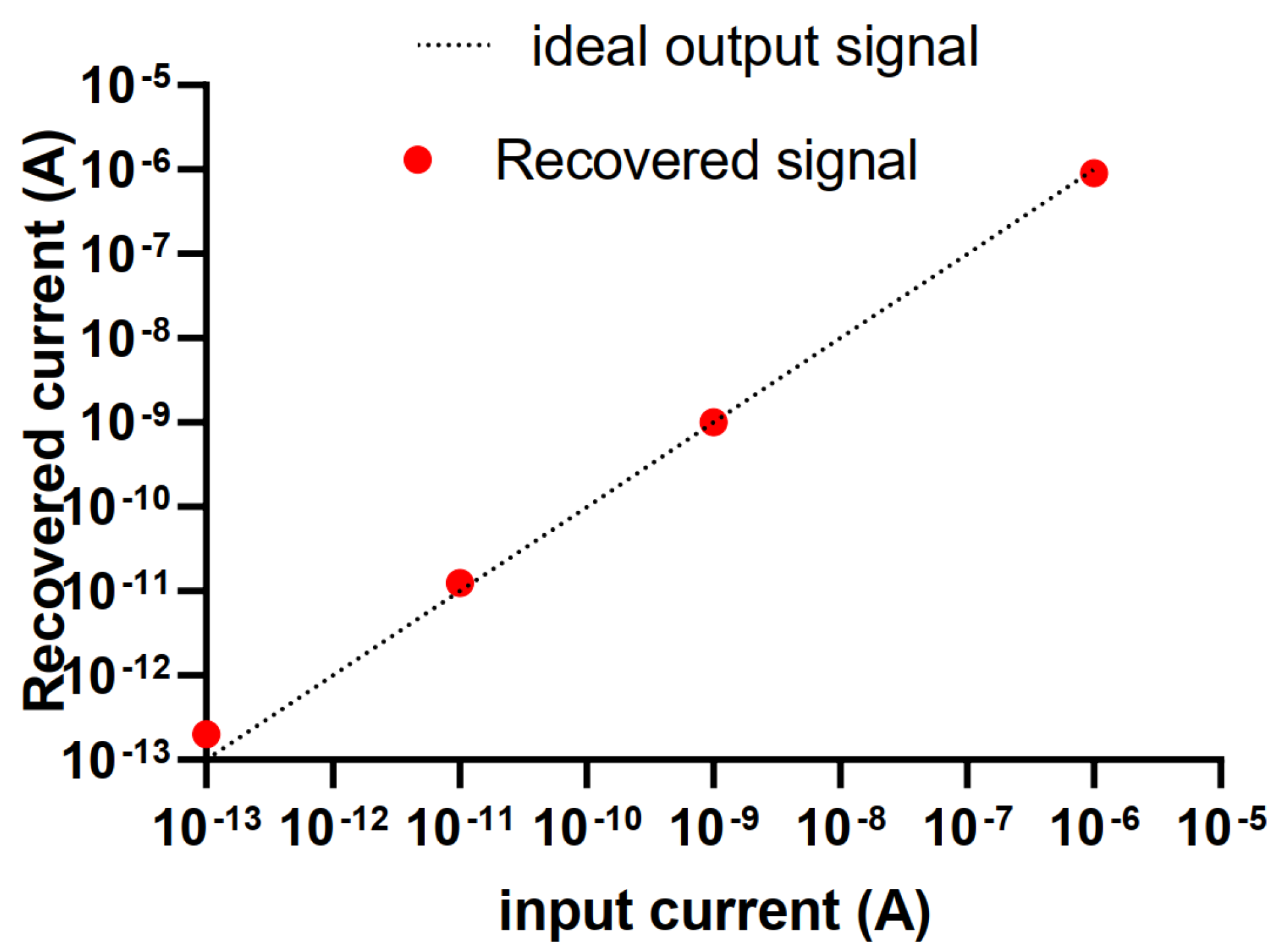
In Figure 17, sinusoidal signals of the amplitude of 100 fA (10 Hz), 1 nA (1 KHz), and 1 A (1 MHz) are used as the input signal, respectively, and results show that recovered signal matches well with the input signal [14].
Table 4 lists the proposed readout circuit performance and compares it with other recent state-of-the-art demonstrations. We added a new metric to the table; “Speed improvement factor”. It is defined as the improvement in output data rate from the use of variable gain settings. This can be estimated as follows. is the threshold voltage of the comparator, and is the integration capacitor. I is the integration current and is the integration time for the 1× current gain setting; 1000I is the integration current and is the integration time for the 1000× current gain setting. We can write Equations (7) and (8) for these two settings.
Equation (9) implies that the circuit can generate the output pulse at a rate 1000 times using the 1000× current gain setting.
4. Conclusions
This paper presents a low-noise current readout circuit using programmable gain setting switches to process a wide input range of currents of 140 dB. The switch arrangement for choosing the programmable gain has been proposed that introduces no phase distortion and it offers flat high-frequency gain. The programmable amplification current stage offers a fast operation of the small current signal and provides a large input dynamic range. The one-bit clockless delta-sigma modulator produces digital output, the input signal is calculated directly from the duty cycle of the pulse output signal. The current amplification enables a higher output data rate for smaller currents. Simulation results in a 0.18 m CMOS process to validate the performance.
Author Contributions
Conceptualization, W.W. and S.S.; methodology, W.W. and S.S.; validation, W.W.; formal analysis, W.W. and S.S.; investigation, W.W. and S.S.; resources, W.W. and S.S.; data curation, W.W.; writing—original draft preparation, W.W.; writing—review and editing, S.S.; visualization, W.W. and S.S.; supervision, S.S.; project administration, S.S.; funding acquisition, S.S. All authors have read and agreed to the published version of the manuscript.
Funding
This research received no external funding.
Conflicts of Interest
The authors declare no conflict of interest.
References
- Rosenstein, J.K.; Wanunu, M.; Merchant, C.A.; Drndic, M.; Shepard, K.L. Integrated nanopore sensing platform with sub-microsecond temporal resolution. Nat. Methods 2012, 9, 487–492. [Google Scholar] [CrossRef] [PubMed]
- Balan, A.; Machielse, B.; Niedzwiecki, D.; Lin, J.; Ong, P.; Engelke, R.; Shepard, K.L.; Drndić, M. Improving Signal-to-Noise Performance for DNA Translocation in Solid-State Nanopores at MHz Bandwidths. Nano Lett. 2014, 14, 7215–7220. [Google Scholar] [CrossRef] [PubMed]
- Crescentini, M.; Bennati, M.; Carminati, M.; Tartagni, M. Noise Limits of CMOS Current Interfaces for Biosensors: A Review. IEEE Trans. Biomed. Circuits Syst. 2014, 8, 278–292. [Google Scholar] [CrossRef]
- Dai, S.; Perera, R.T.; Yang, Z.; Rosensteing, J.K. A 155-dB Dynamic Range Current Measurement Front End for Electrochemical Biosensing. IEEE Trans. Biomed. Circuits Syst. 2016, 10, 935–944. [Google Scholar] [CrossRef]
- Ferrari, G.; Gozzini, F.; Molari, A.; Sampietro, M. Transimpedance amplifier for high sensitivity current measurements on nanodevice. IEEE J. Solid State Circuits 2009, 44, 1609–1616. [Google Scholar] [CrossRef]
- Ibrahim, M.M.R.; Levine, P.M. CMOS transimpedance amplifier for biosensor signal acquisition. In Proceedings of the IEEE International Symposium on Circuits and Systems (ISCAS), Melbourne, Australia, 1–5 June 2014. [Google Scholar]
- Hwang, S.; Trakimas, M.; Sonkusale, S. A Low-Power Asynchronous ECG Acquisition System in CMOS Technology. In Proceedings of the 2010 Annual International Conference of the IEEE Engineering in Medicine and Biology, Buenos Aires, Argentina, 31 August–4 September 2010. [Google Scholar]
- Hwang, S.; Aninakwa, K.; Sonkusale, S. Bandwidth Tunable Amplifier for Recording Biopotential Signals. In Proceedings of the 2010 Annual International Conference of the IEEE Engineering in Medicine and Biology, Buenos Aires, Argentina, 31 August–4 September 2010. [Google Scholar]
- Ibrahim, M.M.R.; Levine, P.M. A 170-dB CMOS TIA with 52-pA input-referred noise and 1-MHz bandwidth for very low current. IEEE Trans. Very Large Scale Integr. Syst. 2017, 25, 1756–1766. [Google Scholar]
- Kim, D.; Goldstein, B.; Tang, W.; Sigworth, F.J.; Culurciello, E. Noise analysis and performance comparison of low current measurement systems for biomedical applications. IEEE Trans. Biomed. Circuits Syst. 2012, 99, 52–62. [Google Scholar]
- Hwang, S.; Sonkusale, S. CMOS VLSI Potentiostat for Portable Environmental Sensing Applications. IEEE Sens. J. 2010, 10, 820–821. [Google Scholar] [CrossRef]
- Mazhab Jafari, H.; Genov, R. Chopper-stabilized bidirectional current acquisition circuits for electrochemical amperometric biosensors. IEEE Trans. Circuits Syst. Regul. Pap. 2013, 60, 1149–1157. [Google Scholar] [CrossRef]
- Ferrari, G.; Farina, M.; Guagliardo, F.; Carminati, M.; Sampietro, M. Ultra-low-noise CMOS current preamplifier from DC to 1 MHz. Electron. Lett. 2009, 45, 1278–1280. [Google Scholar] [CrossRef]
- Ferreira, L.H.C.; Sonkusale, S. A 0.25-V 28-nW 58-dB Dynamic Range Asynchronous Delta Sigma Modulator in 130-nm Digital CMOS Process. IEEE Trans. Very Large Scale Integr. Syst. 2015, 23, 926–934. [Google Scholar] [CrossRef]
- Linares-Barranco, B.; Serrano-Gotarredona, T. On the design and characterization of femtoampere current-mode circuits. IEEE J. Solid State Circuits 2003, 38, 1353–1363. [Google Scholar] [CrossRef]
- Allen, P.; Holberg, D. CMOS Analog Circuit Design, 2nd ed.; Oxford University Press: Oxford, UK, 2002; pp. 471–475. [Google Scholar]
- Amayreh, M.; Manoli, Y.; Keller, M. A 1.85 f Arms/sq(Hz) fully integrated read-out interface for sub-pA current sensing applications. In Proceedings of the ESSCIRC 2017-43rd IEEE European Solid State Circuits Conference, Leuven, Belgium, 11–14 September 2017. [Google Scholar]
- Hsu, C.L.; Hall, D.A. A Current-Measurement Front-End with 160 dB Dynamic Range and 7 ppm INL. In Proceedings of the 2018 IEEE International Solid-State Circuits Conference-(ISSCC), San Francisco, CA, USA, 11–15 February 2018. [Google Scholar]
- Bennati, M.; Thei, F.; Rossi, M.; Crescentini, M.; D’Avino, G.; Baschirotto, A.; Tartagni, M. A Sub-pA ΔΣ Current Amplifier for Single Molecule Nanosensors. In Proceedings of the 2009 IEEE International Solid-State Circuits Conference-Digest of Technical Papers, San Francisco, CA, USA, 8–12 February 2009. [Google Scholar]
Figure 1.
Bidirectional current amplification.

Figure 2.
Programmable low-frequency current gain stage.

Figure 3.
Conventional series switch based high frequency current gain stage.

Figure 4.
Shows a realization of a gain of 10. Off-switches will still contribute to parasitic capacitance affecting the overall gain and stability.
Figure 4.
Shows a realization of a gain of 10. Off-switches will still contribute to parasitic capacitance affecting the overall gain and stability.

Figure 5.
Proposed programmable high-gain stage using a T-network.

Figure 6.
Current follows through the two feedback capacitor during amplification state.

Figure 7.
Current follows through the ground during off state.

Figure 8.
Top architecture of the wide dynamic range current readout circuit.

Figure 9.
Current splitter for programmable reference current generation.

Figure 10.
Half Current splitting circuit shown in (a) based on the splitting equivalent representation of a single transistor in (b).
Figure 10.
Half Current splitting circuit shown in (a) based on the splitting equivalent representation of a single transistor in (b).

Figure 11.
Low-noise amplifier.

Figure 12.
Hysteresis comparator.

Figure 13.
Current reader layout.

Figure 14.
Current gains of 1000×, 100×, 10×, and 1×.

Figure 15.
Input referred noise density of the current reader with the gain of 1000×, 100×, 10× and 1×.
Figure 15.
Input referred noise density of the current reader with the gain of 1000×, 100×, 10× and 1×.

Figure 16.
Input-referred integrated noise of the current reader with the gain of 1000×, 100×, 10× and 1×.
Figure 16.
Input-referred integrated noise of the current reader with the gain of 1000×, 100×, 10× and 1×.

Figure 17.
Recovered input current.


Table 1.
Current gain in each stage.
| Total Gain | First Stage Gain | Second Stage Gain |
|---|---|---|
| 1000× | 50× | 20× |
| 100× | 50× | 2× |
| 10× | 10× | 1× |
| 1× | 1× | 1× |
Table 2.
Table of comparison with relevant architecture.
| Parameter | Value |
|---|---|
Table 3.
Input referred integrated current noise (rms).
| Gain 1000× | Gain 100× | Gain 10× | Gain 1× | |
|---|---|---|---|---|
| 100 Hz | 8 fA | 8 fA | 9 fA | 26 fA |
| 10 KHz | 0.13 pA | 0.13 pA | 0.25 pA | 2.53 pA |
| 1 MHz | 0.051 nA | 0.054 nA | 0.118 nA | 1.113 nA |
Table 4.
Table of comparison with relevant architecture.
| [4] | [5] | [17] | [18] | [19] | This Work * | |
|---|---|---|---|---|---|---|
| Technology (m) | 0.18 | 0.35 | 0.35/0.5 | 0.18 | 0.18 | 0.18 |
| Power supply (V) | 1.8 | 3 | 3 | 1.8 | 3.3 | 1.8 |
| 3 dB Signal bandwidth (MHz) | 1.4 | 4 | 0.1 | 1.25 | 0.0039 | 0.85 |
| Dynamic range (dB) | 155.1 | 95.9 | 80 | 160 | 74 | 140 |
| Area (mm) | 0.091 | 0.34 | 0.6 | 0.2 | 0.5 | 1.015 |
| Power consumption (mW) | 9.4 | 13.5 | 7 | 0.3 | 23 | 10.3 |
| Speed improvement factor | 1× | 1× | 1×1 | 1× | 1× | 1000× |
* Simulation result.
© 2020 by the authors. Licensee MDPI, Basel, Switzerland. This article is an open access article distributed under the terms and conditions of the Creative Commons Attribution (CC BY) license (http://creativecommons.org/licenses/by/4.0/).
Share and Cite
MDPI and ACS Style
Wang, W.; Sonkusale, S. An Approach for a Wide Dynamic Range Low-Noise Current Readout Circuit. J. Low Power Electron. Appl. 2020, 10, 23. https://0-doi-org.brum.beds.ac.uk/10.3390/jlpea10030023
AMA Style
Wang W, Sonkusale S. An Approach for a Wide Dynamic Range Low-Noise Current Readout Circuit. Journal of Low Power Electronics and Applications. 2020; 10(3):23. https://0-doi-org.brum.beds.ac.uk/10.3390/jlpea10030023
Chicago/Turabian StyleWang, Wei, and Sameer Sonkusale. 2020. "An Approach for a Wide Dynamic Range Low-Noise Current Readout Circuit" Journal of Low Power Electronics and Applications 10, no. 3: 23. https://0-doi-org.brum.beds.ac.uk/10.3390/jlpea10030023
Note that from the first issue of 2016, this journal uses article numbers instead of page numbers. See further details here.