1. Introduction
As CMOS technologies scale down, supply voltage requirements have been reduced. The need for transistor size and power supply scaling has been motivated by the rapid increase in the market of portable devices (i.e., for Internet of Things and biomedical applications) and their need for low-voltage, low-power circuitry to increase battery time [
1]. Analog circuits, contrary to their digital counterpart, have not easily adapted to the rapid supply voltage downscaling, mostly due to the fact that the threshold voltages have been reduced at a much lower rate than the supply voltage and currently represent a significant fraction of the nominal supply voltage in current deep sub-micrometer CMOS technologies [
2]. The minimum supply voltage of circuits with operational amplifiers is determined by the headroom
of the differential input stage. Signals in conventional op-amp topologies usually have a mid-supply common-mode component to allow for maximum and symmetrical peak-peak signal swing close to the supply voltage. This requires a minimum supply
in conventional architectures. With the current values of supply and threshold voltages, this biasing no longer allows transistors to operate in strong inversion in conventional amplifiers.
Several techniques have been proposed to solve this problem. Bulk driven (BD) amplifiers [
3,
4,
5,
6,
7] can operate with reduced supply voltages; however, the bulk-to-source transconductance
of MOS transistors is significantly lower than their gate-to-source transconductance
(by approximately a factor 5). An additional degradation factor of BD circuits comes from the fact that PMOS differential pairs are commonly used in the input stage of BD amplifiers. PMOS transistors have an additional factor 3–5 lower transconductance gain than NMOS transistors with the same bias current and dimensions. This degrades the performance of bulk driven circuits in terms of bandwidth, noise, DC offset and causes their figure of merit
and power efficiency to be lower than that of their gate driven (GD) counterparts for similar bias currents (
is the static power dissipation, and CL is the load capacitance). An additional disadvantage of BD circuits is that their input swing is severely limited in order to prevent forward biasing of the MOS transistor substrate-source and substrate-drain PN junctions that can lead to destructive latch-up. This constrains BD circuits to operate in subthreshold with supply voltages lower than
V and with small gain-bandwidth products (GBWs, typically lower than
). Circuits with floating gates input differential pairs have been reported for the implementation of gate driven low supply circuits with transistors in saturation [
8]. Since they are based on capacitive voltage dividers at the input terminals of the op-amp, they are also subject to GBW, noise, and offset degradation. Circuits with quasi-floating gate transistors overcome these problems and can operate with low supply voltages, but they require a DC offset cancellation circuit to prevent saturation of the output nodes [
9]. Two non-conventional techniques of digital-based (DB) operational transconductance amplifiers (OTAs) have been proposed for the implementation of low supply voltage systems. One of them is based on “time signal processing” and is characterized by relatively small and large signal FOM [
10]. The other one is based on the digital implementation of differential pairs using inverters [
11]. This technique has large FOMs and has been refined to introduce digital calibration [
12], but it is characterized by relatively low CMRR and open-loop gain, and their voltage gain accuracy (when implementing amplifiers) does not depend on component ratios.
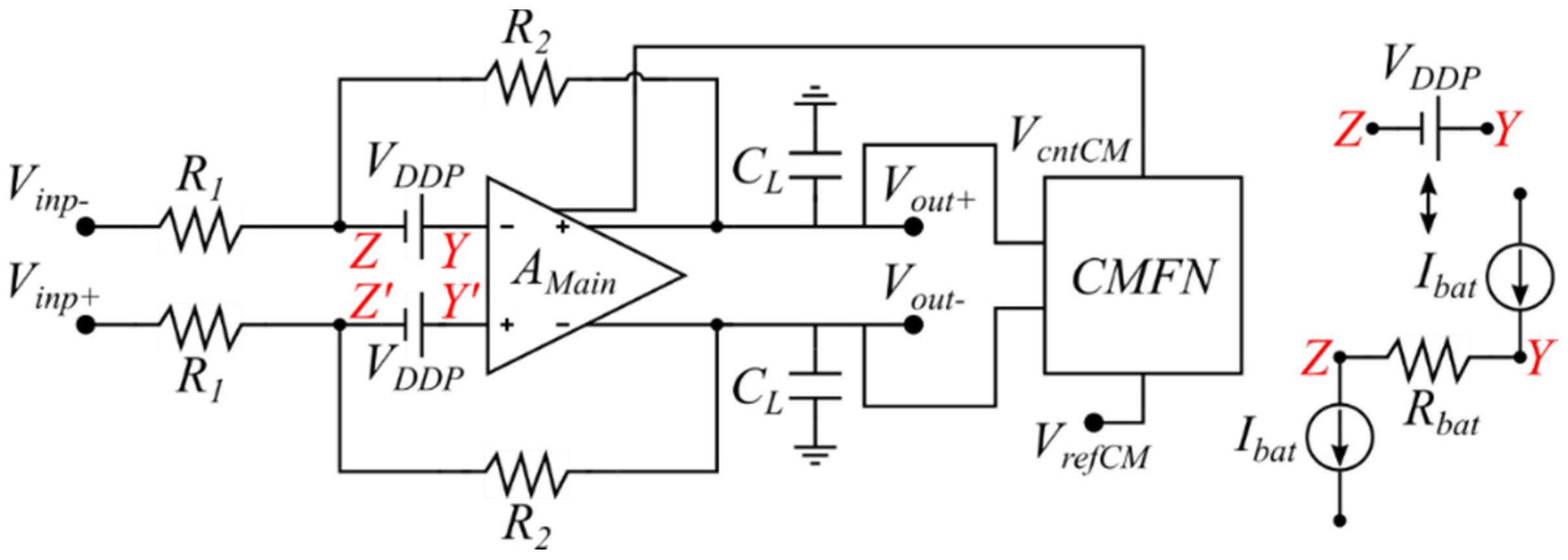
Two families of gate driven low voltage techniques with transistors in saturation are based on DC level shifting techniques, which cause the op-amp input terminals to operate very close to a supply rail. This provides headroom
for the op-amp NMOS differential input stage, which is close to the total supply voltage
and allows reduction by almost a factor 2 of the minimum supply voltage
. One of the families is based on
voltage-mode techniques and uses floating DC voltage sources [
13]. This technique inserts floating DC voltage sources (see
Figure 1) with value
inserted in series with the op-amp input terminals (an NMOS input differential pair is assumed). The floating DC sources are implemented, as shown in
Figure 1, with a resistor
and matches sinking and sourcing current sources
that satisfy
. They allow signal nodes Z, Z’ to operate at the mid-supply voltage and maintain at the same time the op-amp input terminals at a voltage
(close to
), which reduces the minimum supply requirements by close to a factor two
. A drawback of this approach is the additional noise introduced by the resistors
. A
current-mode family of low voltage amplifiers is based on current source DC level shifting techniques. They apply common-mode level shifting currents
at the op-amp input terminals. These currents pull the voltage level at the input terminals of the op-amp to a voltage
close to the upper rail. The injected currents
must satisfy the condition
where
is the common-mode voltage of the input signals
and
, and
is the reference common-mode output voltage.
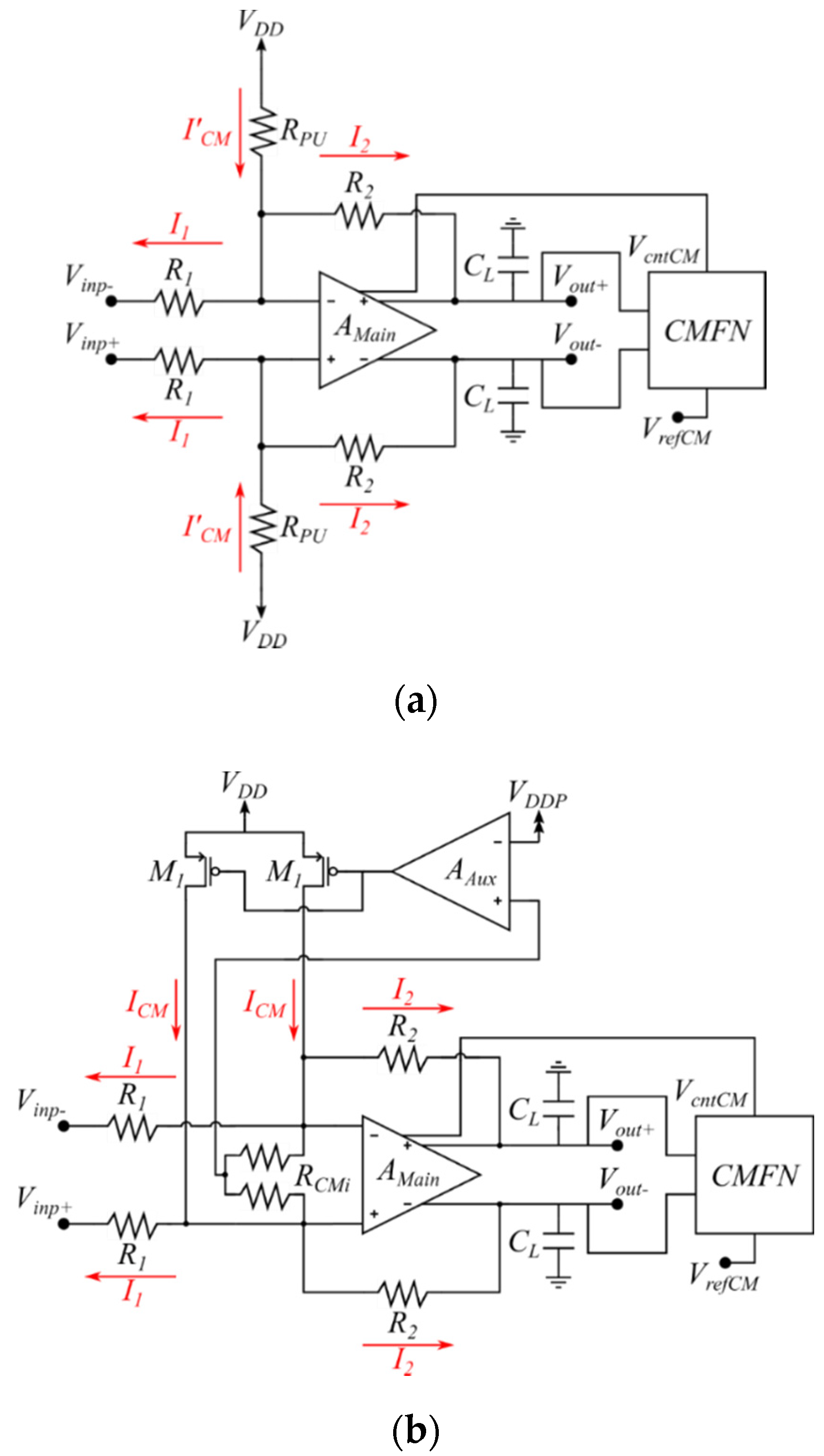
In the implementation of
Figure 2 [
14,
15], pull-up resistors
with fixed value
are used to generate constant currents
which assume a constant input common-mode component (usually
) and constant supply
. Due to the fixed value of
the scheme is not functional if common-mode input signals are present or if there are variations in the supply voltage
. Another drawback is that for
close to
, the pull-up resistors
are required to have values
this leads to significant degradation of the amplifier’s bandwidth and offset since
is an integral part of the amplifier’s feedback network β, and
decreases the value of the feedback factor β. This degrades the bandwidth (BW) given by
. It can also significantly increase the output DC offset voltage and noise.
Figure 2 illustrates another implementation of the current source level shifting scheme reported in [
16]. In this implementation level, shifting currents
, which include a component dependent on the common-mode input signal
, are injected at the op-amp input terminal. The common-mode input voltage
of the op-amp input terminals is sensed using resistors
in the main amplifier. An auxiliary amplifier
drives transistors M1, M1′; this generates matched currents
which leads to
. This scheme is functional with variable supply voltage and variable common-mode input voltage
but the common-mode sensing resistors
also lead to bandwidth and offset degradation. This is to a much lower degree than the scheme of
Figure 2 since no condition is placed on the value of
which can take values
to minimize BW and offset degradation. The three fully differential low-voltage amplifier schemes of
Figure 1 and
Figure 2 require a relatively complex output common-mode feedback network that can also operate with a low supply voltage.
In this paper, a current-mode DC level shifting technique for the implementation of fully differential low supply voltage amplifiers and transistors operating in saturated mode is proposed, which overcomes the problems listed above. It is functional with variable supply voltages. It has high common-mode input signal rejection, high open-loop gain, and high small signal and large signal FOMs. Its main advantage is that it does not require a low-voltage output common-mode feedback network, and it does not include additional resistors in the main amplifier feedback network that degrades BW, DC offset, and noise. The proposed circuit is described in the next
Section 2.
2. Circuit Description of the Implementation of Proposed Current Mode Low Voltage Technique
We assume in the following discussion, without loss of generality, fully differential Miller op-amps operating from dual symmetrical supplies
, with NMOS input differential stages and with input/output signals having quiescent common-mode voltages that correspond to the mid-supply value
. Operation at low voltage is achieved in the proposed circuit by shifting also the common-mode voltage of the amplifier input terminals
to a voltage
close to the upper rail
. This is done by injecting level shifting currents sources
at the op-amp input terminals (nodes Z, Z’).
Figure 3 shows the scheme of the proposed amplifier that includes, besides the main amplifier, also an auxiliary amplifier
. The transistor-level implementation of the fully differential op-amp and the auxiliary amplifier are shown in
Figure 4a,b, respectively.
The level shifting common-mode current sources have a value
where
is the common-mode voltage of
and
that might include common-mode signals, and
is the reference nominal common-mode output voltage (usually to maximize and obtain symmetrical output signal swing
but it can take a different value). These currents are generated by the single-ended auxiliary amplifier
. This amplifier has its positive input terminal connected to
and has three outputs, two of them with factor 10 current scaling/replication. The output
is connected to the negative input terminal of
at node Q. This node is also connected to two resistors with values
and to a resistor with value
. The main amplifier input signals
,
are applied to one of the terminals of the resistors with value
, and the output common-mode reference voltage
is applied to one terminal of the resistor
. Due to negative feedback, the current delivered by the output terminal
to node Q has a value
. Outputs
and
of the auxiliary amplifier deliver accurate scaled-up replicas (by factor 10) with value
to nodes Z, Z’ of the main amplifier. Besides pulling up the op-amp common-mode input voltage
to a value
at the same time, currents
lead to complementary output signals with a common-mode voltage
. It can be seen that the auxiliary amplifier performs simultaneously as a common-mode sensor for
,
, as a DC level shifter for the op-amp input terminals, and as a replacement for the output common-mode feedback network. Besides working as a level shifter with input common-mode rejection, it generates complementary output signals with an output common-mode voltage
. Scaling down by factor 10 the current delivered by
with resistors
and
in the auxiliary amplifier is done with the purpose of reducing power dissipation (and increasing power efficiency of the proposed scheme) since in this case, the output of the auxiliary amplifier has a current
. Transistors M6-M8 in
of
Figure 4b are also scaled down by a factor 10 with the same purpose.
The main op-amp is designed as a fully differential two-stage AB (Miller) op-amp. Resistors
in the input stage of
Figure 4a implement a resistive local common-mode feedback network [
17]. They set the DC operating point at nodes X, X’ to value
and provide complementary signals at these nodes. This is required since the op-amp does not have an output common-mode feedback network (CMFN). The output stage is a high power-efficient “free class AB amplifier” [
18] that provides approximately symmetrical positive and negative slew rates not limited by the quiescent current of the output stage.
and
are used to set the quiescent output current and to provide dynamic class AB operation to the output stage.
and
are conventional Miller compensation elements.
3. Results
The proposed low voltage amplifier of
Figure 2 is simulated using cadence design framework with ±300 mV dual supplies, in a commercial 180 nm technology that has a nominal supply voltage
using
and
in three different cases: (a) Applying common-mode input signals
; (b) Applying a single-ended input
,
; (c) Applying complementary input signals with zero common-mode input voltage
,
. The input test signal
is a 100 kHz sinusoidal signal with a 20 mV peak amplitude. Resistors
and
are set for a nominal gain
.
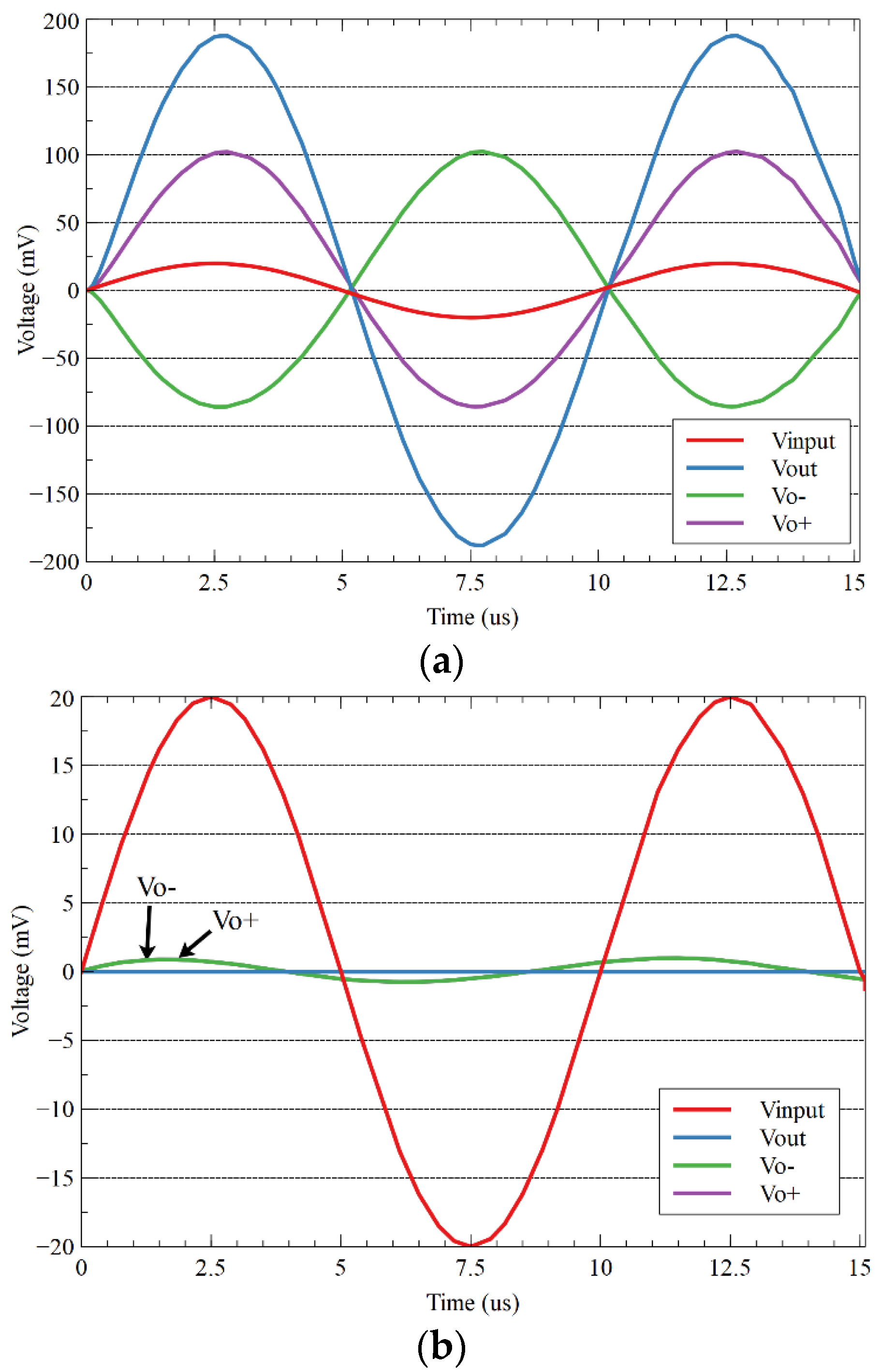
Figure 5a shows the differential output voltage
and the single-ended complementary outputs
and
for the last two cases, while
Figure 5b shows the differential output
and single-ended outputs
and
for common-mode inputs. Notice that the results are the same for the last two cases. This verifies the high rejection of common-mode input signals with the generation of complementary output signals at mid-supply in the proposed scheme. It also shows operation with a total supply
.
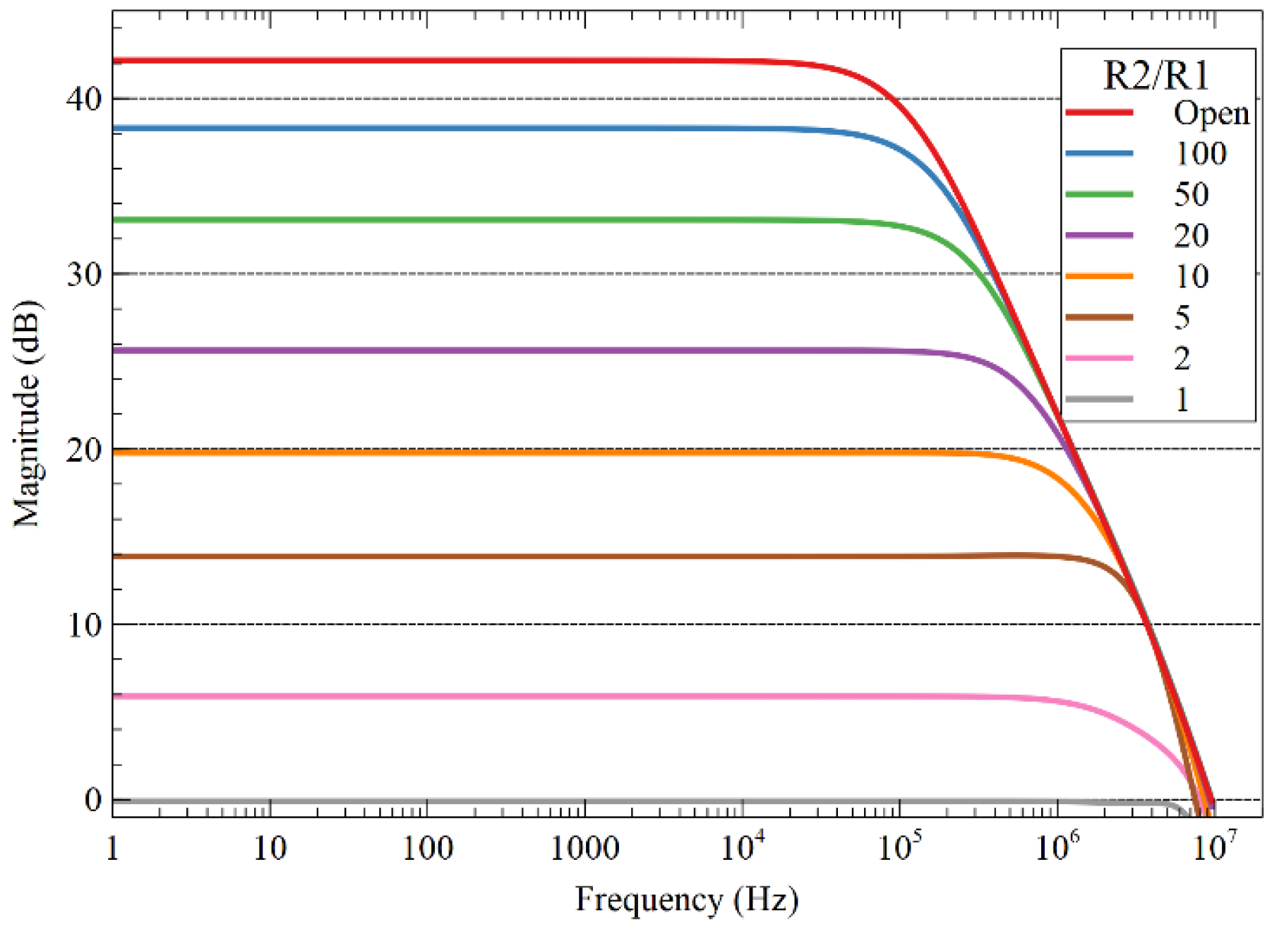
Figure 6 shows the simulated frequency response of the amplifier for nominal gains: 1, 2, 10, 20, 50, 100, and open loop. The DC open-loop gain is found to be
. The unity gain frequency of the open-loop response is
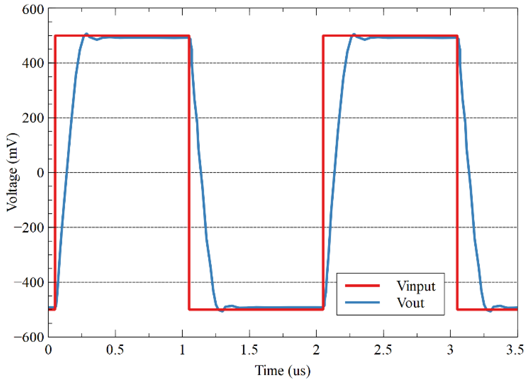
. The slew rate of 8.4 V/µs is calculated from the pulse response of
Figure 7, with a
,
differential input pulse, and in this case, the gain of the amplifier is set to 1.
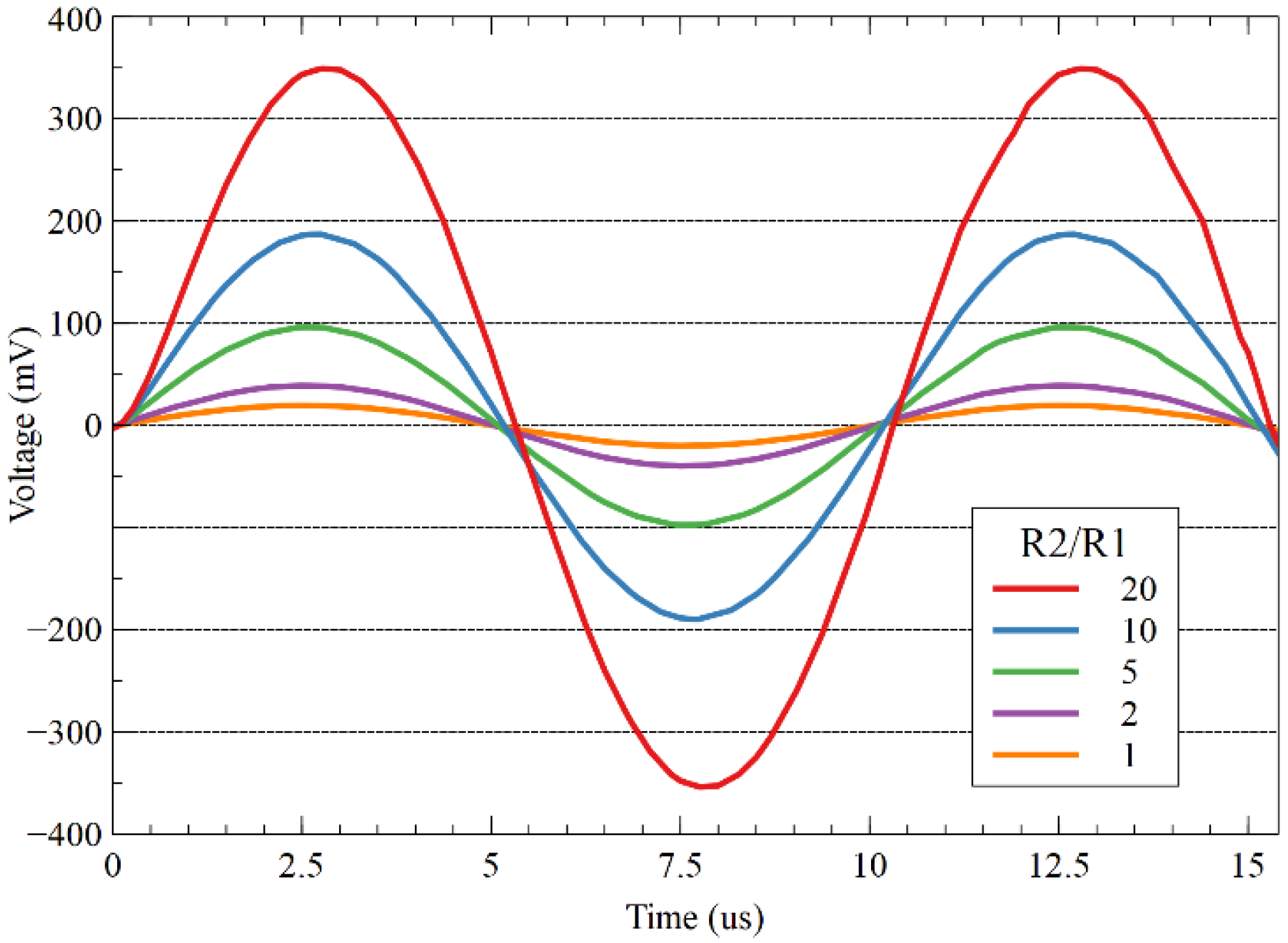
Figure 8 shows the transient simulation of
at different gains for a
,
peak sinusoidal differential input signal.
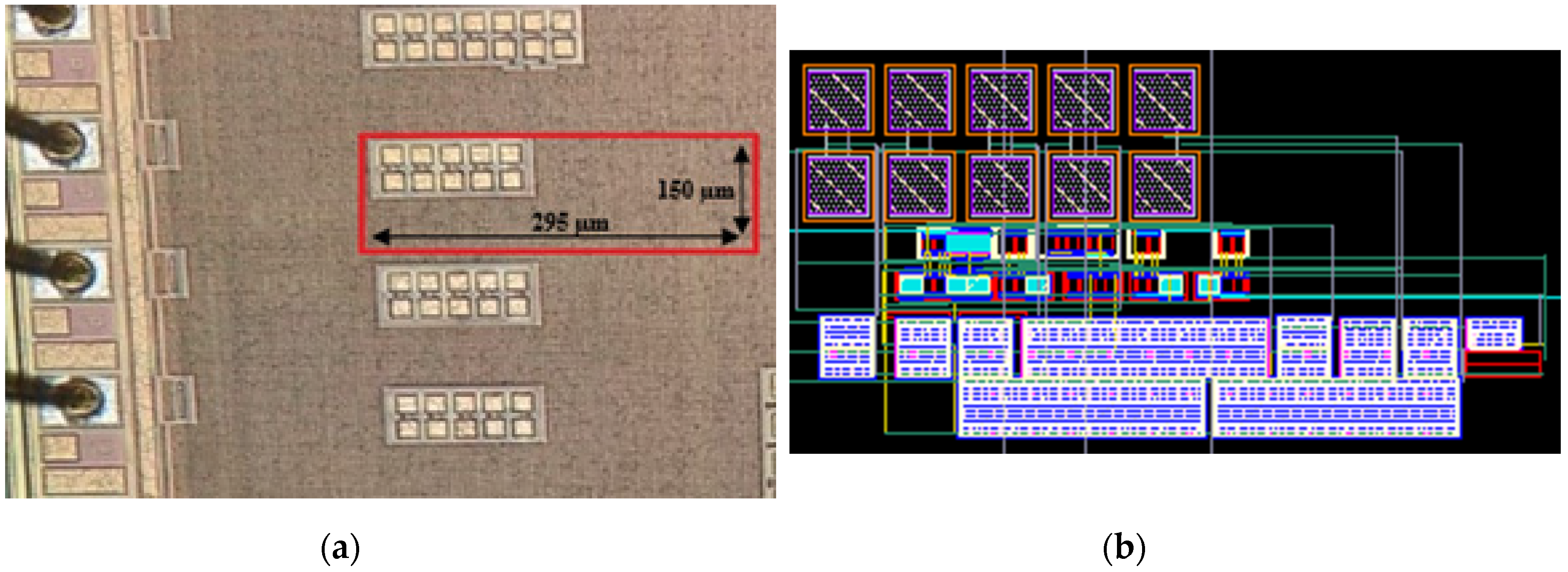
The proposed circuit is fabricated in a TSMC 180 nm CMOS process for a fixed gain of 10 with resistors
and
. Functionality with a gain of
is verified with dual supplies ±300 mV and
and with
bias current. An input offset of
is measured.
Figure 9 shows the chip microphotograph and circuit layout design.
Table 1 shows the design parameters of the proposed circuit.
Table 2 shows the parameters obtained from the characterization in the cadence of the circuit with
bias current. This table also contains the comparison with other gate driven and bulk driven low voltage amplifiers. Corner analysis of the performance parameters of the proposed amplifier at three temperatures is included in
Table 3.


