A 100 MHz 0.41 fJ/(Bit∙Search) 28 nm CMOS-Bulk Content Addressable Memory for HEP Experiments


Department of Physics and Italian National Institute for Nuclear Physics (INFN), University of Milano-Bicocca, 20126 Milan, Italy
*
Author to whom correspondence should be addressed.
J. Low Power Electron. Appl. 2020, 10(4), 35; https://0-doi-org.brum.beds.ac.uk/10.3390/jlpea10040035
Submission received: 8 September 2020
/
Revised: 18 October 2020
/
Accepted: 19 October 2020
/
Published: 28 October 2020
(This article belongs to the Special Issue Low-Power CMOS Analog and Digital Circuits and Filters)
Abstract
:This paper presents a transistor-level design with extensive experimental validation of a Content Addressable Memory (CAM), based on an eXclusive OR (XOR) single-bit cell. This design exploits a dedicated architecture and a fully custom approach (both in the schematic and the layout phase), in order to achieve very low-power and high-speed performances. The proposed architecture does not require an internal clock or pre-charge phase, which usually increase the power request and slow down data searches. On the other hand, the dedicated solutions are exploited in order to minimize parasitic layout-induced capacitances in the single-bit cell, further reducing the power consumption. The prototype device, named CAM-28CB, is integrated in the deeply downscaled 28 nm Complementary Metal-Oxide-Semiconductor (CMOS) Bulk (28CB) technology. In this way, the high transistor transition frequency and the intrinsic lower parasitic capacitances allow the system speed to be improved. Furthermore, the high radiation hardness of this technology node (up to 1Grad TID), together with the CAM-28CB high-speed and low-power performances, makes this device suitable for High-Energy Physics experiments, such as ATLAS (A Toroidal LHC ApparatuS) at Large Hadron Collider (LHC). The prototype operates at a frequency of up to 100 MHz and consumes 46.86 µW. The total area occupancy is 1702 µm2 for 1.152 kb memory bit cells. The device operates with a single supply voltage of 1 V and achieves 0.41 fJ/bit/search Figure-of-Merit.
1. Introduction
Content Addressable Memories (CAMs), also known as Associative Memories (AM), are very popular digital devices used for data storage and data processing applications. They are exploited, for example, as look up tables for IP addresses in network routers and find applications as well in data compression algorithms, database management, and image pattern recognition processing [1,2,3,4,5]. In recent years, they have also been exploited in Artificial Neural Networks [6,7] and hyperdimensional computing for Artificial Intelligence (AI) [8], where highly efficient associative memories tend to be a common specification. Usually, CAM devices are also an important building block in the front-end for High-Energy Physics experiments, such as ATLAS and CMS (Compact Muon Solenoid) at LHC. In such systems, they are exploited for fast searching operations, especially for particle tracks recognition in the Trigger system (for filtering the huge amount of data coming from the detectors [4]).
The CAM is a static memory whose main function is to conduct a bit-to-bit comparison of an input digital word (searching data) and all of the data stored inside the memory itself. When the input data match the stored data, the CAM simultaneously returns an acknowledge bit (MATCH) and the address of the matching data inside the memory bank. The fully parallel comparison only lasts one single clock cycle, allowing fast searching operations at a hardware level w.r.t. other software implementations. However, this architecture might lead to an increase in power consumption, due to the contemporary and continuous comparison activity in every device cell [3]. For this reason, different hardware solutions, based on particular single-bit cells [3,4,5,9,10,11] or various power saving algorithms [11,12,13], have been explored in the past.
The novelty of this work, compared to the state-of-the-art, is the presentation of a Content Addressable Memory developed with a full-custom design approach in the 28 nm CMOS-Bulk node (CAM-28CB). The highly downscaled technology node offers a speed increase, without a power consumption increase (with the standard digital design flow, a device speed increase and a size reduction, up to a factor of 3, result, compared to the CMOS 65 nm node [3,9]). Moreover, the main aim of this work is to produce aggressive power reduction achieved with a full-custom design, both in the schematic and the layout phase. The core scheme relies on a fast asynchronous architecture, with only logic XOR or NOR cells and without internal clocking or a pre-charge phase, which are characteristics that usually tend to decrease CAM speed performances and sometimes require several clock cycle latency periods before the output is provided. In terms of the layout side, the full-custom approach allows the minimization of area occupancy and layout parasitic capacitances, reducing the dynamic power consumption. A detailed analysis of the layout-induced parasite’s impact on the overall CAM power consumption will be provided in the following. Furthermore, the 28 nm CMOS-Bulk node exhibits an excellent rad-hard performance, as demonstrated in [14], up to 1Grad-TID. Being resilient against long-term radiation damage is a crucial requirement in every system for High-Energy Physics and particle physics. Thanks to its performances, the proposed CAM meets the specifications needed for the Fast-TracKer (FTK) processor to be integrated in the next ATLAS upgrade, where CAM stages are placed very close to the detectors and a certain radiation hardness is required. Moreover, CMOS-Bulk is preferred to Fully Depleted Silicon-on-Insulator (FD-SoI), which exhibits a higher sensitivity due to radiation-induced charge entrapped in the substrate oxide. In detail, the proposed prototype (CAM-28CB) is able to store 64 different digital words with an 18-bit length (for an overall 1.152 kb storage capability). This meets the specifications of the ATLAS application, whilst increasing the digital word length does not have a significant impact on the energy spent per search per bit. On the other hand, increasing the amount of stored data may reduce the maximum device speed, especially at a low supply voltage. The prototype operates with a single supply voltage ranging from 0.85 up to 1 V, with a working frequency of up to 100 MHz. The prototype core area is 1702 µm2. Its overall average power consumption (both static and dynamic power) is 46.86 µW, which is equivalent to 0.41 fJ/(Bit∙Search).
The rest of the paper is organized as follows. Section 2 presents the general architecture and the transistor-level design of the proposed CAM device. Information about the layout-induced parasitic capacitances and their impact on the power consumption is provided. In Section 3, complete experimental validation of the prototype test chip is provided. The overall CAM performances are compared with the state-of-the-art in this section. At the end of the paper, conclusions are drawn.
2. The CMOS 28NM CAM Design
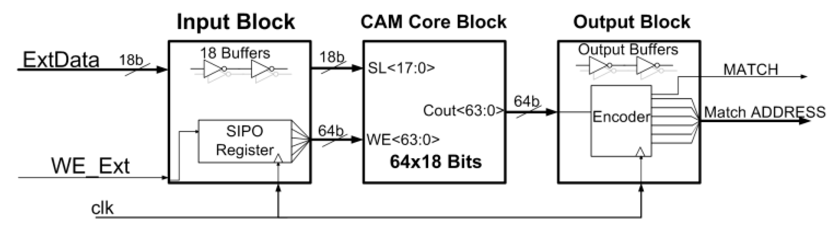
The CAM-28CB proposed in this paper is composed of three main blocks: An Input Block; a Core Block; and an Output Block. The overall functional scheme is illustrated in Figure 1.
The Input Block stage contains 18 input buffers and a Serial-Input-Parallel-Output (SIPO) synchronous register. This stage, as well as the entire CAM, operates in two different modes: WRITE and SEARCH. Every 18-bit digital word that must be stored (or searched) inside the memory is provided by the ExtData bus signal (generated from an external setup). An external Write Enable signal (WE_Ext) asserts the CAM operation mode. In the case of the WRITE mode, this signal feeds the input of the SIPO register, which, in turn, provides the Write Enable signals (WE<63:0>) for each CAM row. In this way, 64 18-bit data, coming from the ExtData bus, are correctly stored inside the 64 rows of the CAM, once every clock cycle. In order to correctly operate, ExtData must be synchronous with the SIPO clock: ExtData changes every clock rising edge and at the same time, the WE signal shifts to the following memory row. Lastly, before reaching the CAM memory bank and being stored, digital words from ExtData are buffered into the Search Lines (SL<17:0>) bus, and are the same for storage or search operations. Driving the data lines is a power-hungry operation and, for this reason, these buffers’ power consumption must be taken into account for complete device characterization.
The second stage, as shown in Figure 1, is the 1.152 kb CAM Core Block, performing both storage and searching operations in a completely asynchronous way. The particular architecture of the single-bit cell will be illustrated in the following text. Lastly, the prototype design also includes the output stages, which drive the output load for testing purposes, and a digital encoder, which provides the address of the matching data for developing an appropriate measurement setup.
Therefore, the device has three main output signals: The MATCH signal (logic ‘1’ if the searched word has been found inside the memory core); the 8-bit MATCH address bus; and the SIPO output. The MATCH signal and MATCH bus only operate during the search mode, while the SIPO register is only active during the write phase.
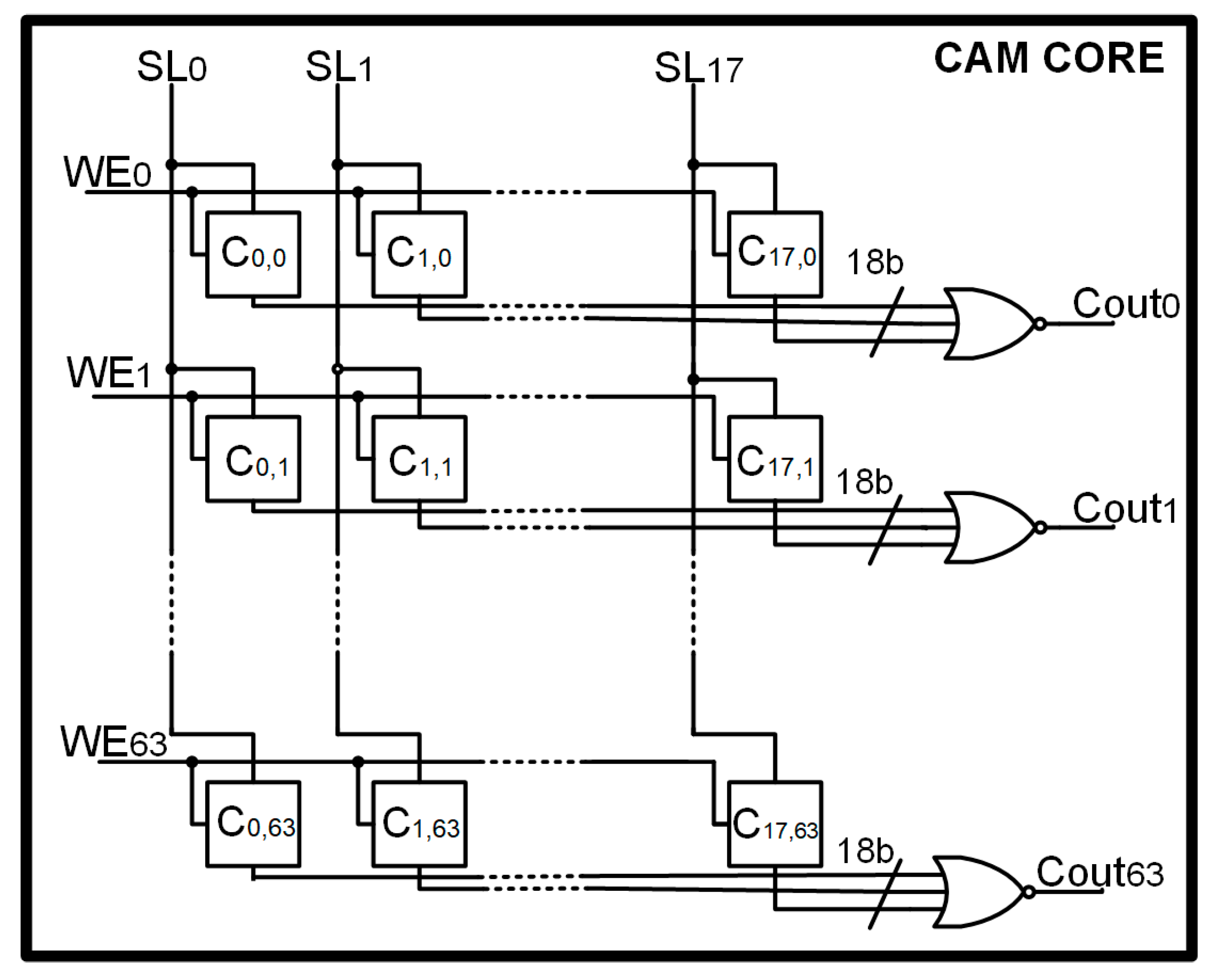
2.1. The CAM Core
The CAM-28CB Core stores 64 digital words (j = 0–63) of 18-bit (i = 0–17). Each one of the 18 single-bit cells in the j-th row is connected to an NOR gate, whose output (Coutj) feeds the final encoder located in the Output Block. Figure 2 illustrates a schematic view of the Core Block. Each cell located in the j-th row shares the same WE signal, in order to store every bit of a digital word in the same clock cycle during the WRITE phase.
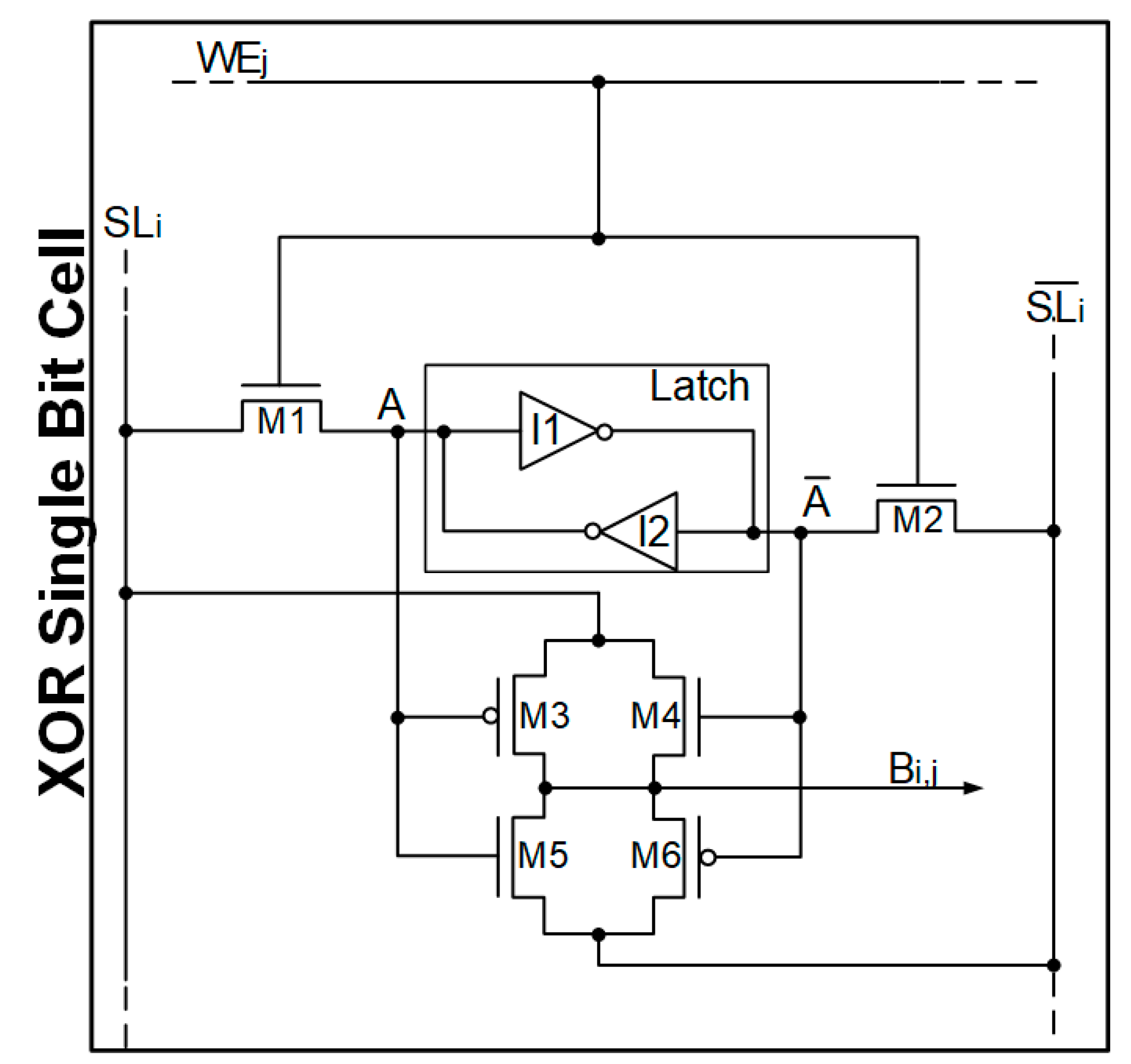
The single-bit cell is able to store a single bit, while, during the SEARCH phase, it performs an XOR logic operation. A schematic of the single-bit cell is shown in Figure 3. It is composed of a latch (cross coupled inverters), which stores the bit, two Metal-Oxide-Semiconductor (MOS) transistors (M1 and M2) used as switches, and four MOS transistors (M3, M4, M5, and M6) performing the XOR operation between searched data (coming from the SL bus) and stored data.
As already stated, the CAM works in two different operating modes: WRITE and SEARCH.
Consider the case of a single-bit cell in the WRITE mode operation. The WRITE mode is set by the corresponding WEj signal. In this case, both M1 and M2 transistors operate as a switch connecting the i-th SL bit with the latch. In this way, data on the SLi are stored inside the cell Ci,j.
On the other hand, in SEARCH mode, M1 and M2 are open. MOS M3, M4, M5, and M6 perform an XOR operation between the data stored inside the i-th latch and the data on the SLi. Only in the case of a match between searched and stored data does the cell output bit Bij’s becomes logic low.
The 18 outputs of the j-th row feed an 18-bit NOR gate that only turns quickly if every Bij node is logic low, asserting that a complete data match occurred in that row.
2.2. Power Consumption Evaluation
Power consumption is one of the most important performance indicators for static memories. In this design, it is possible to achieve very low-power performances thanks to the full-custom design approach in the layout phase. The parasitic capacitances of each switching node are reduced compared to standard cell designs and minimized according to the stringent 28 nm layout rules.
The static power consumption is assumed to be negligible, since its contribution to the overall CAM power is in the order of a few pA/bit and for this reason, only the dynamic power consumption must be taken into account.
The dynamic power consumption can be divided into two main contributions: The power of the SL buffers and the power of logic (for every row) and latches (inside the single-bit cells).
The CAM dynamic power in write mode is given by the well-known Equation (1):
where is the overall capacitance in write mode per single bit, fCLK is the clock frequency, and VDD is the supply voltage. The overall capacitance in WRITE mode is composed of the parallelity between the CA,W capacitance (the equivalent capacitance to the ground of the A setting node in Figure 3) and the SL parasitic capacitance (CP,SL), as shown in Equation (2):
Specifically, in order to achieve a very low CP,SL, the SL is realized with a minimum width/minimum length metal 1 connection, which is evaluated at 0.46 fF by the parasitic extraction tool.
The CA,W is, in turn, the equivalent capacitance of the A setting node, given by Equation (3):
where CG,I1 is the I1 gate capacitance, CD,I2 is the I2 output capacitance, CG,M35 represents the input capacitance of both M3 and M5 transistors, and CBij is the total capacitance on the XOR single-bit output node, described by Equation (4):
where CG,NORj is the input capacitance of the following j-th NOR gate in the same row, CD,M35 represents the output capacitance of both M3 and M5 transistors, and CD,M46 represents the output capacitance of both M4 and M6 transistors.
CA,W ≅ CG,I1 + CD,I2 + CG,M35 + CBij + CP,A ≈ 1.25 fF,
CBij ≅ CG,NORj + CD,M35 + CD,M46 + CP,LAYOUT B ≈ 1.15 fF,
Moreover, the total capacitance in WRITE mode at node A also depends on the routing parasitics in both A and Bij nodes, and more specifically, on CP,LAYOUT A and CP,LAYOUT B. Unfortunately, it is not possible to avoid vias when designing these nodes because of the 28 nm stringent layout rules. In order to minimize the impact of parasitics, these nodes are designed to have the minimum number of vias and the minimum area of metal possible. In this way, it is possible to achieve a very low value for parasitic capacitance in these nodes (0.21 and 1.05 fF for CP,LAYOUT A and CP,LAYOUT B respectively).
On the other hand, the dynamic power in search mode (more important, since this is the usual operating mode of the CAM) is given by Equation (5):
where is the overall capacitance per bit given by Equation (6):
Table 1 shows some of the most important parasitic routing and small-signal capacitance values of the MOS transistor in both search and write mode. All transistors in the design have a minimum size (W/L = 100 nm/30 nm) to minimize the total gate capacitance CG (mainly, the overlap capacitance given by Cox∙W∙L) and area occupancy.
Table 1 demonstrates that the transistor MOS small signal capacitance is typically negligible in 28 nm CMOS-Bulk technology in terms of the effects on the power and speed. On the other hand, this also forces dedicated layout solutions able to reduce both the CP,LAYOUT B and CP,LAYOUT SL term as much as possible in SEARCH mode, since they are dominant and increase the power.
From post-layout simulations, the falling time for the ij-th cell output node (Bij) is 82.8 ps. This results in a 0.012 V/ps output slew-rate that will need an average switching current of approximately 8.37 µA, provided by the SL buffers. From Equation (5), assuming a 100 MHz clock frequency and 0.85 V supply voltage, applying capacitance values from Table 1, PWSEARCH is 75 nW per bit.
3. Experimental Results
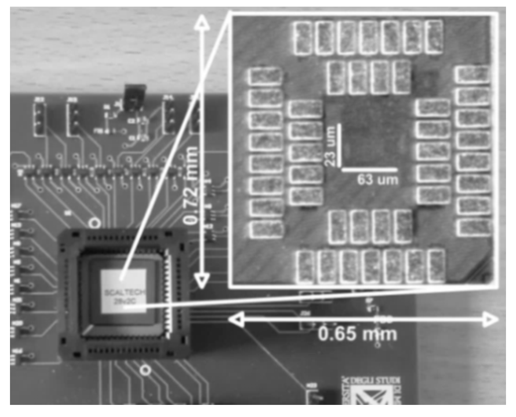
A chip photo of the integrated CAM-28CB device is shown in Figure 4.
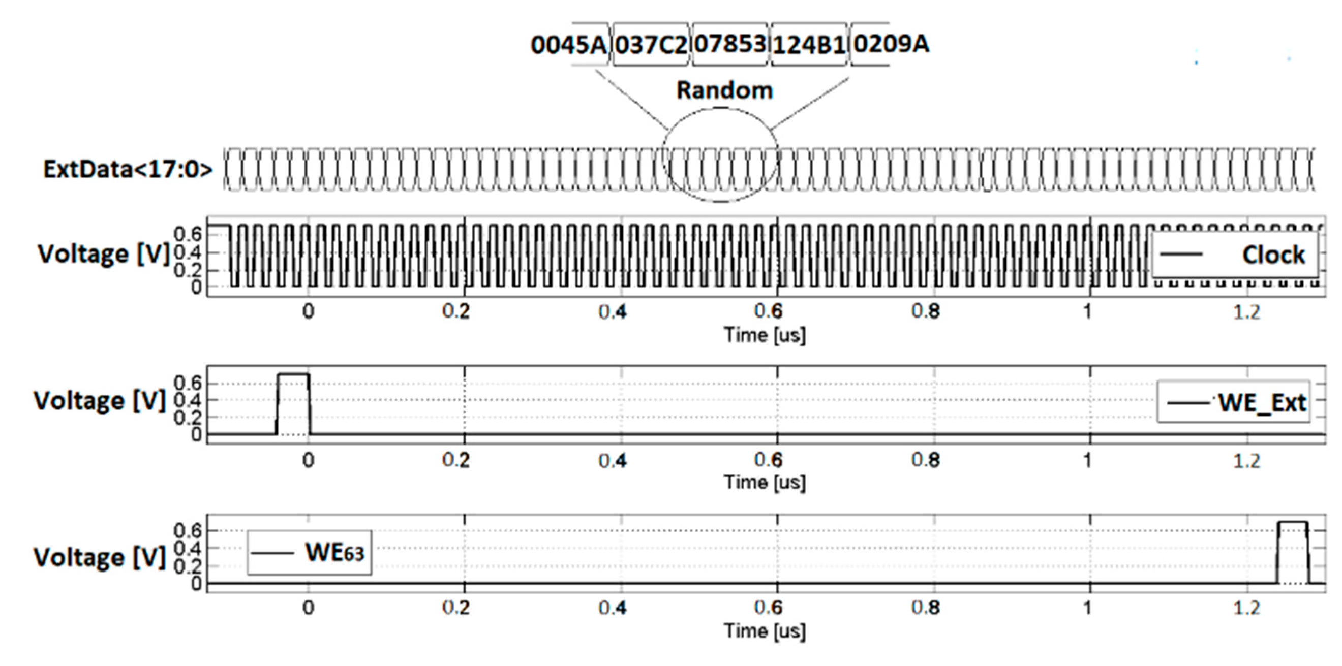
For testing purposes, the memory is filled with a random 64 data pattern (WRITE Mode, Figure 5). Afterwards the SEARCH mode runs with one pattern for four different input patterns, repeated cyclically, in order to test several minutes of device activity. These patterns are used to measure CAM performances in terms of the power consumption and speed. The four patterns are as follows:
The first three patterns are limited to only 128 different searched data values, periodically repeated.
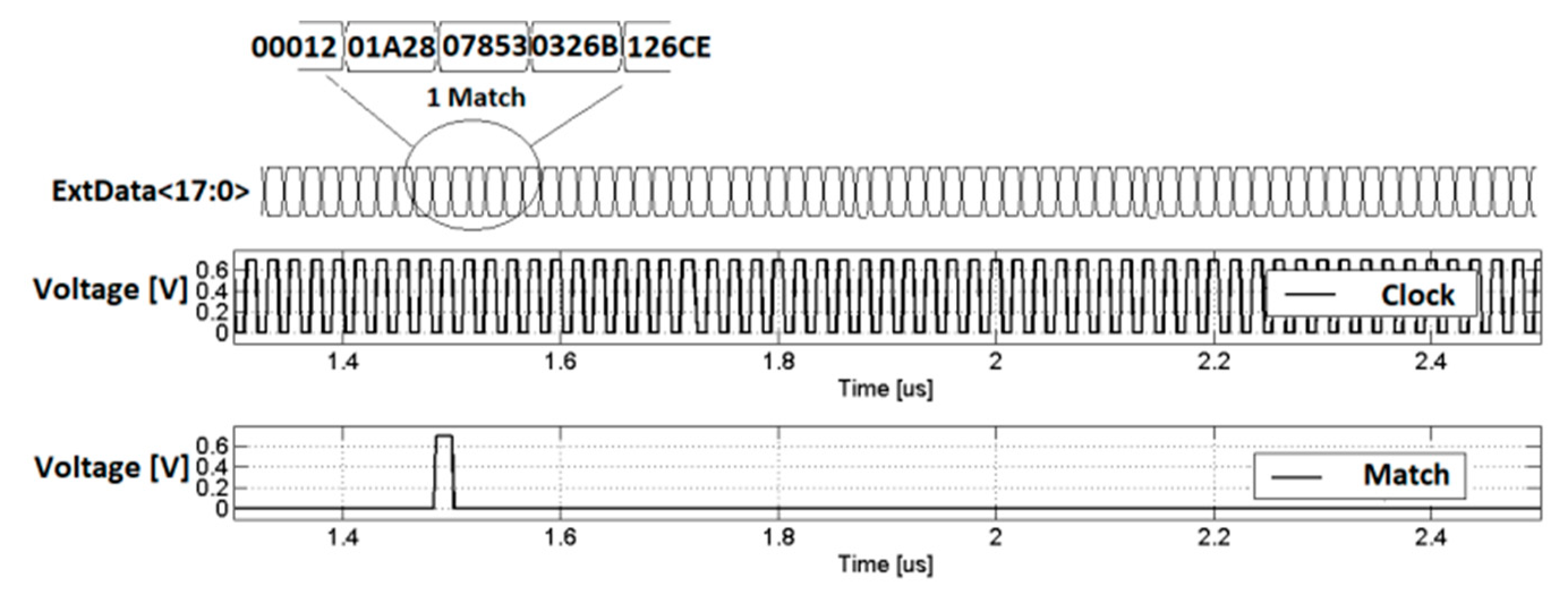
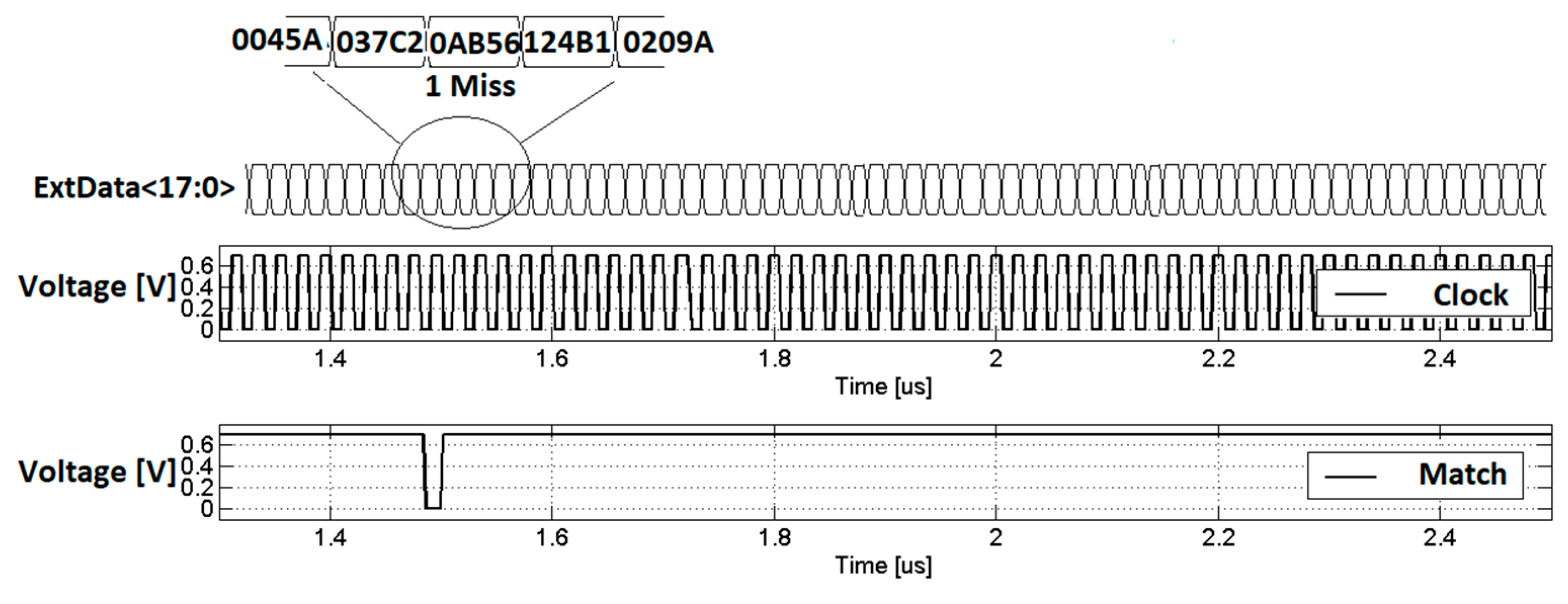
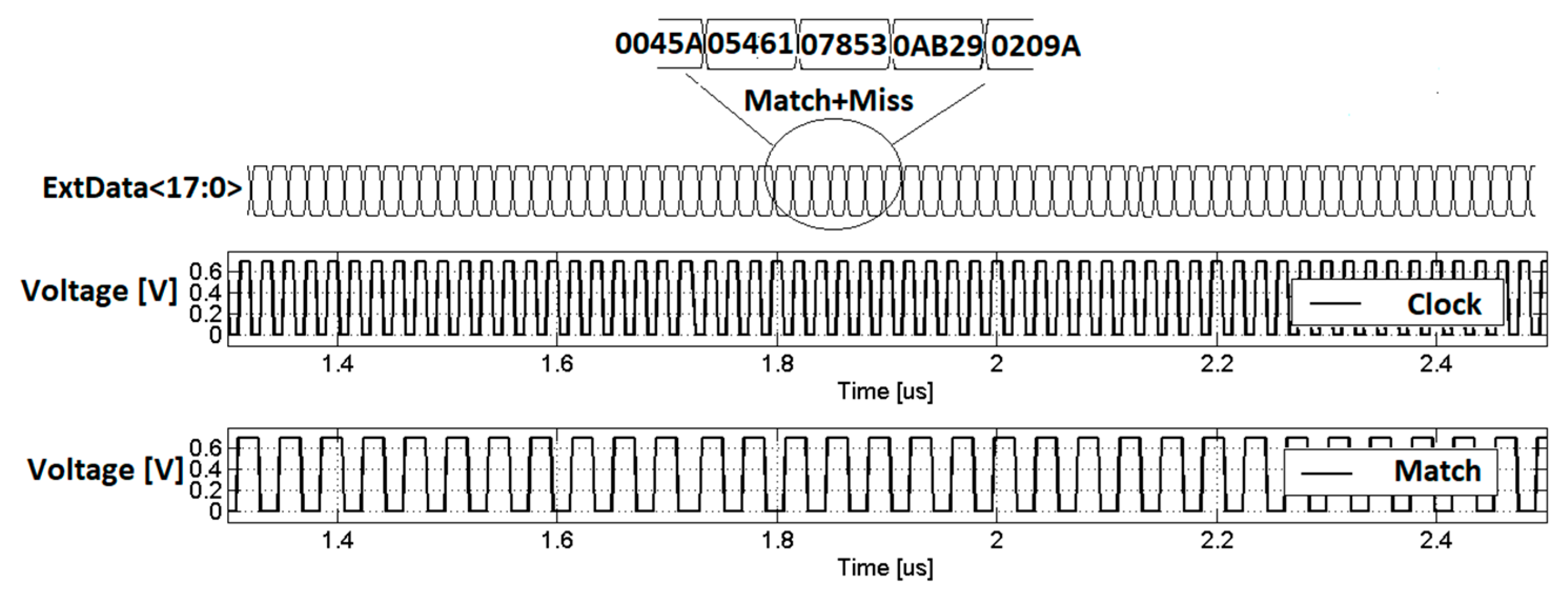
Figure 5, Figure 6, Figure 7 and Figure 8 show the time diagrams, taken from a Logic Analyzer (LA), of some of the most important input and output signals. A specific Pattern Generator module, embedded in the LA, synchronizes the input signal with the CAM clock and outputs.
The last pattern is a fully Random Pattern generated by a Field Programmable Gate Array (FPGA). In this case, a dedicated algorithm, which exploits a Fibonacci Linear-Feedback Shift-Register (LFSR), is used to randomly generate every possible data value from 1 to 218−1. In this way, only 64 random matches occur every 218 clock cycles, emulating CAM real-life utilization.
After the WRITE mode operation is concluded, the ExtData bus starts to switch as a function of the selected pattern. The input (WE_Ext) and output (WE63) signals of the SIPO register in write mode are also shown in Figure 5, in order to assert the start and end of the WRITE phase. The clock frequency in this case is set to 100 MHz. The power consumption of the prototype has been measured, cyclically repeating these patterns and also spreading the supply voltage and clock frequency. The power () is mainly dynamic and can be in first approximation expressed as a function of the total number of bits of the memory (Nbit,i), switching at frequency fCLK,i (usually different bit switches at different frequencies) and the equivalent capacitance (Cbit) per bit, according to Equation (7):
depends on the chosen pattern. In the simplest case (MIN, MAX, and Medium pattern), and meaning that the MSB switches every clock cycle, the second MSB switches at half the clock frequency, and so on. In this way, Cbit can be easily calculated and is equal to 1.914 fF, in perfect agreement with the simulated post-layout net-list power.
For a random pattern, it is not possible to determine the fCLK,i term, since every i-th bit randomly switches. For this reason, it is necessary to exploit Equation (8):
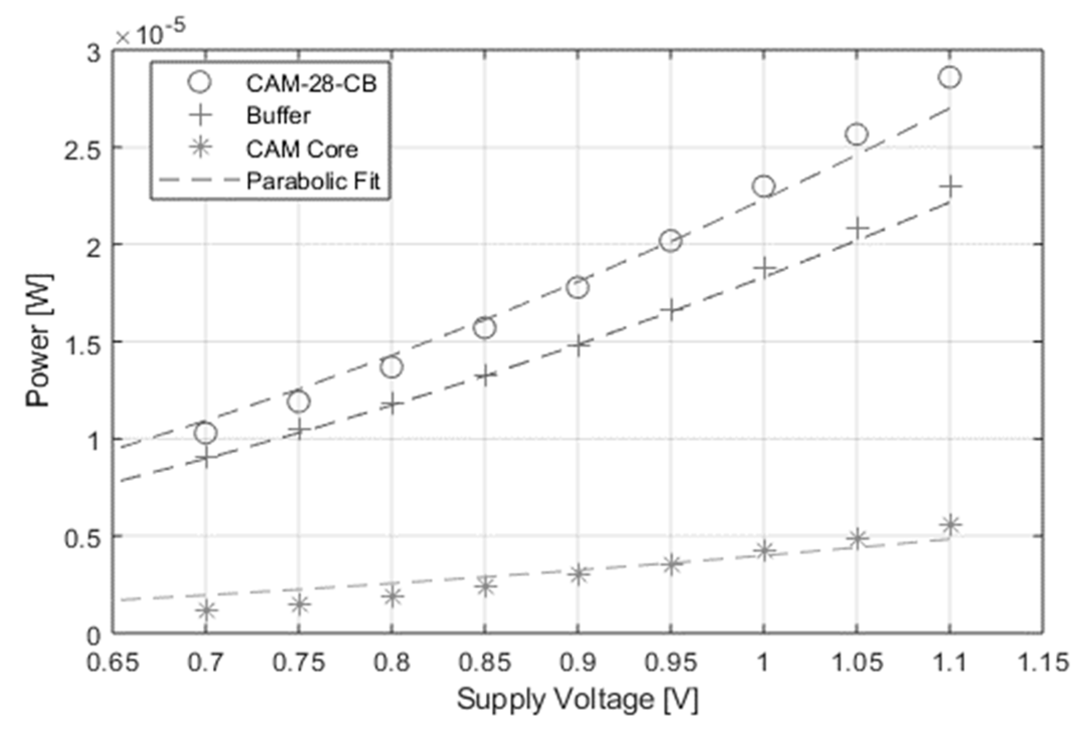
where Nbit,eq is the equivalent number of bits switching at clock frequency (fCLK) and is equal to 378.15, which is a much lower value than the overall number of bits (1152), as expected. The vs. VDD at a 100 MHz clock frequency has been plotted in Figure 9, fitting with the parabolic behavior vs. VDD presented in Equation (7). Figure 10 shows the vs. clock frequency at a 0.85 V supply voltage and compares the measurement results with the linear fitting vs. fCLK derived from Equation (4). In both Figure 9 and Figure 10, the power has been divided into buffer and core power consumption, in order to better highlight all the contributions to the overall power consumption of the prototype.
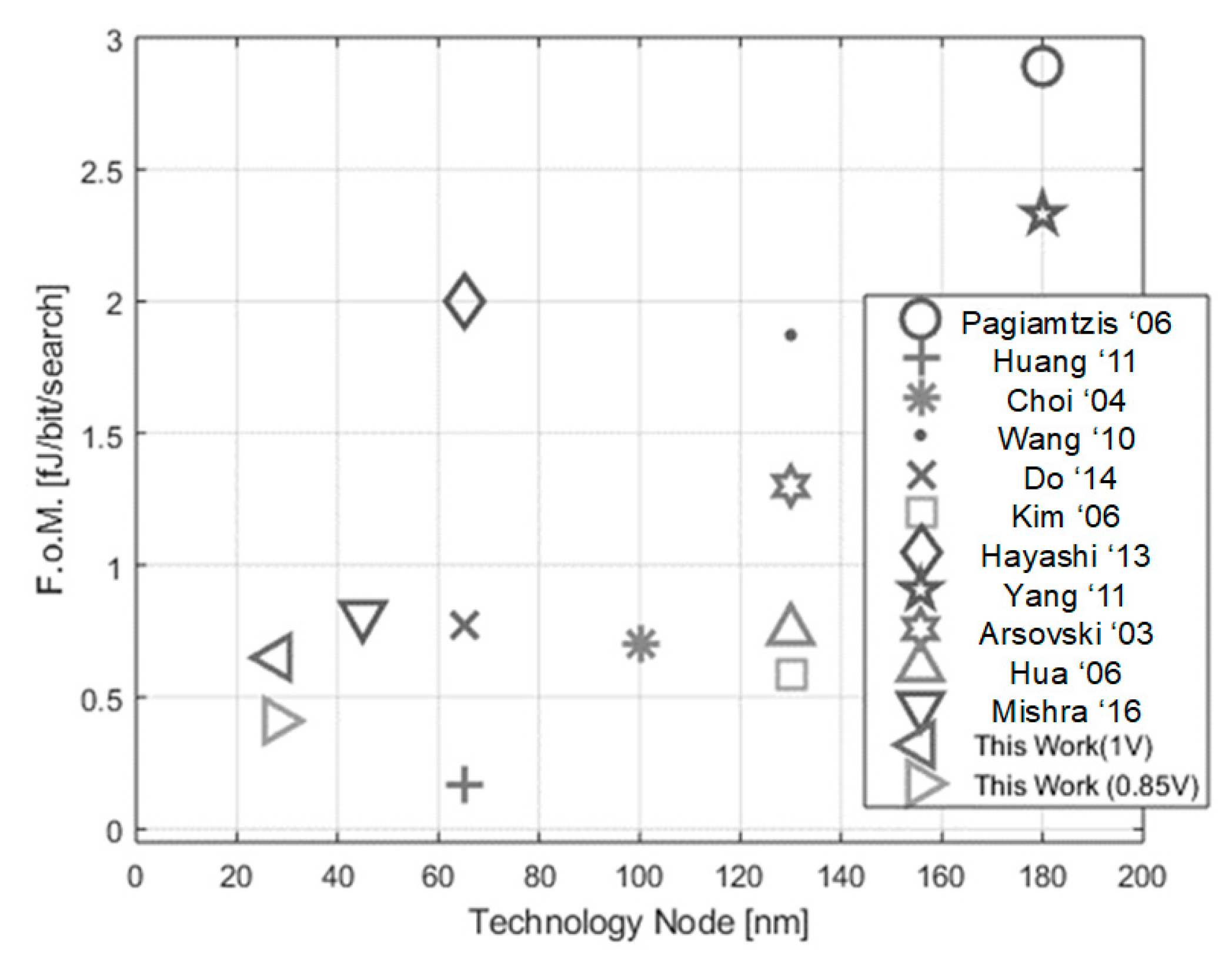
Finally, the overall performance of this memory prototype has been compared with the state-of-the-art of the associative memories available in the literature. More specifically, Table 2 reports the most important performance and Figure 11 shows the Figure-of-Merit (F.o.M.) vs. CMOS Technology node of this prototype and the literature [2,3,9,11,12,13,15,16,17,18,19]. The adopted F.o.M. is given by Equation (9):
where PWCAM is the total power consumption expressed in Watt (W), fCLK is the clock frequency (100 MHz), and SIZE is the CAM memory size (1.152 kb).
Thanks to the 28 nm CMOS-Bulk node and the customized layout solutions that minimize the parasitic capacitance contribution in the XOR single-bit cell, this work has achieved one of the lowest F.o.M. in the literature. Moreover, it reaches a factor of 3 in size reduction compared to the 65 nm technology node [15]. On the other hand, the same factor is not reached in the power consumption as a consequence of the fact that the channel length (on which the device size depends) scales faster than the parasitic capacitance (on which the power consumption depends, according to Equation (7)) with the technology node [16]. Moreover, the purpose of the CAM-28-CB is to conduct power consumption reduction through the single-bit XOR cells’ architecture and parasitic capacitance minimization in a strongly downscaled technology such as CMOS 28 nm, and for this reason, the proposed CAM architecture does not implement any advanced algorithm for power saving, such as pipeline or hierarchical SL. At the same time, the CAM-28-CB performances are comparable and even improved compared to other nanoscale technologies.
4. Conclusions
This work presents measurement validation of a 0.85 V 1.152 kb Content Addressable Memory that operates at a searching frequency of up to 100 MHz. The device is realized in 28 nm CMOS-bulk technology, exploiting the low-power and low-capacitance nodes. The architecture, based on XOR single-bit cells and full-custom layout solutions, allows a very low power consumption and small device dimensions to be achieved. The memory operates from a single 0.85 V supply voltage, consumes 46.86 µW dynamic power, and occupies 1702 µm2, resulting in one of the lowest F.o.M. presented in the literature.
Author Contributions
Conceptualization, F.F. and A.B.; Methodology, Software, Validation, Formal Analysis, Writing Original Draft, F.F.; Writing Review & Editing, Visualization, Supervision, Project Administration, A.B. All authors have read and agreed to the published version of the manuscript.
Funding
This research received no external funding.
Conflicts of Interest
The authors declare no conflict of interest.
References
- Pagiamtzis, K.; Sheikholeslami, A. Content-Addressable Memory (CAM) Circuits and Architectures: A Tutorial and Survey. IEEE J. Solid-State Circuits 2006, 41, 712–727. [Google Scholar] [CrossRef]
- Pagiamtzis, K.; Sheikholeslami, A. A low-power content-addressable memory (CAM) using pipelined hierarchical search scheme. IEEE J. Solid-State Circuits 2004, 39, 1512–1519. [Google Scholar] [CrossRef]
- Huang, P.T.; Hwang, W. A 65 nm 0.165 fJ/Bit/Search 256×144 TCAM Macro Design for IPv6 Lookup Tables. IEEE J. Solid-State Circuits 2011, 46, 507–519. [Google Scholar] [CrossRef]
- Annovi, A.; Baschirotto, A.; Beretta, M.M.; Biesuz, N.V.; Citraro, S.; Crescioli, F.; De Matteis, M.; Fary, F.; Frontini, L.; Giannetti, P.; et al. A XOR-based associative memory block in 28 nm CMOS for interdisciplinary applications. In Proceedings of the 2015 IEEE International Conference on Electronics, Circuits, and Systems (ICECS), Cairo, Egypt, 6–9 December 2015; pp. 392–395. [Google Scholar]
- Fary, F.; Mangiagalli, L.; Pipino, A.; Resta, F.; De Matteis, M.; Baschirotto, A. A 200 MHz 0.65fJ/(Bit·Search)1.152kb pipeline content addressable memory in 28 nm CMOS. In Proceedings of the 2017 13th Conference on Ph.D. Research in Microelectronics and Electronics (PRIME), Giardini Naxos, Italy, 12–15 June 2017; pp. 353–356. [Google Scholar]
- Gong, W.; Liang, J.; Li, D. Design of high-capacity auto-associative memories based on the analysis of complex-valued neural networks. In Proceedings of the 2017 International Workshop on Complex Systems and Networks (IWCSN), Doha, Qatar, 8–10 December 2017; pp. 161–168. [Google Scholar]
- Tanaka, G.; Nakane, R.; Takeuchi, T.; Yamane, T.; Nakano, D.; Katayama, Y.; Hirose, A. Spatially Arranged Sparse Recurrent Neural Networks for Energy Efficient Associative Memory. IEEE Trans. Neural Netw. Learn. Syst. 2020, 31, 24–38. [Google Scholar] [PubMed]
- Karunaratne, G.; Le Gallo, M.; Cherubini, G.; Benini, L.; Rahimi, A.; Sebastian, A. In-memory hyperdimensional computing. Nat. Electron. 2020, 3, 327–337. [Google Scholar] [CrossRef]
- Choi, S.; Sohn, K.; Lee, M.-W.; Kim, S.; Choi, H.-M.; Kim, D.; Cho, U.-R.; Byun, H.-G.; Shin, Y.-S.; Yoo, H.-J. A 0.7fJ/bit/search, 2.2ns search time hybrid type TCAM architecture. IEEE J. Solid-State Circuits 2004, 40, 254–260. [Google Scholar] [CrossRef]
- Li, H.-Y.; Chen, C.-C.; Wang, J.-S.; Yeh, C. An AND-Type Match-Line Scheme for High-Performance Energy-Efficient Content Addressable Memories. IEEE J. Solid-State Circuits 2006, 41, 1108–1119. [Google Scholar] [CrossRef]
- Wang, C.-C.; Hsu, C.-H.; Huang, C.-C.; Wu, J.-H. A Self-Disabled Sensing Technique for Content-Addressable Memories. IEEE Trans. Circuits Syst. II 2010, 57, 31–35. [Google Scholar] [CrossRef]
- Do, A.T.; Yin, C.; Velayudhan, K.; Lee, Z.C.; Yeo, K.S.; Kim, T.T.-H. 0.77 fJ/bit/search Content Addressable Memory Using Small Match Line Swing and Automated Background Checking Scheme for Variation Tolerance. IEEE J. Solid-State Circuits 2014, 49, 1487–1498. [Google Scholar] [CrossRef]
- Kim, Y.-D.; Ahn, H.-S.; Park, J.-Y.; Kim, S.; Jeong, D.-K. A Storage- and Power-Efficient Range-Matching TCAM for Packet Classification. In Proceedings of the 2006 IEEE International Solid State Circuits Conference—Digest of Technical Papers, San Francisco, CA, USA, 6–9 February 2006; pp. 587–596. [Google Scholar]
- Pezzotta, A.; Zhang, C.M.; Jazaeri, F.; Bruschini, C.; Borghello, G.; Faccio, F.; Mattiazzo, S.; Baschirotto, A.; Enz, C. Impact of GigaRad Ionizing Dose on 28 nm bulk MOSFETs for future HL-LHC. In Proceedings of the 2016 46th European Solid-State Device Research Conference (ESSDERC), Lausanne, Switzerland, 12–15 September 2016; pp. 146–149. [Google Scholar]
- Hayashi, I.; Amano, T.; Watanabe, N.; Yano, Y.; Kuroda, Y.; Shirata, M.; Dosaka, K.; Nii, K.; Noda, H.; Kawai, H. A 250-MHz 18-Mb Full Ternary CAM with Low-Voltage Matchline Sensing Scheme in 65-nm CMOS. IEEE J. Solid-State Circuits 2013, 48, 2671–2680. [Google Scholar] [CrossRef]
- Yang, M.T.; Liao, K.; Welstand, R.; Teng, C.; Sy, W.; Chen, Y.; Dutta, R.; Chidambaram, P.R.; Han, M.; Du, Y.; et al. RF and mixed-signal performances of a low cost 28nm low-power CMOS technology for wireless system-on-chip applications. In Proceedings of the 2011 Symposium on VLSI Technology—Digest of Technical Papers, Honolulu, HI, USA, 14–16 June 2011; pp. 40–41. [Google Scholar]
- Arsovski, I.; Sheikholeslami, A. A current-saving match-line sensing scheme for content-addressable memories. In Proceedings of the 2003 IEEE International Solid-State Circuits Conference, 2003. Digest of Technical Papers (ISSCC), San Francisco, CA, USA, 13 February 2003; pp. 304–305. [Google Scholar]
- Hua, C.-H.; Peng, C.-W.; Hwang, W. A noise-tolerant matchline scheme with XOR-based conditional keeper for energy-efficient TCAM. In Proceedings of the 2006 IEEE International Symposium on Circuits and Systems, Island of Kos, Greece, 21–24 May 2006; pp. 4–10. [Google Scholar]
- Mishra, S.; Mahendra, T.V.; Dandapat, A. A 9-T 833-MHz 1.72-fJ/Bit/Search Quasi-Static Ternary Fully Associative Cache Tag with Selective Matchline Evaluation for Wire Speed Applications. IEEE Trans. Circuits Syst. I 2016, 63, 1910–1920. [Google Scholar]
Figure 1.
Content Addressable Memory (CAM)-28-CB top view schematic diagram.

Figure 2.
CAM-28-CB core schematic diagram.

Figure 3.
XOR single-bit cell (Ci,j) schematic diagram.

Figure 4.
CAM-28-CB chip board and photo.

Figure 5.
CAM-28-CB experimental time diagram (WRITE MODE).

Figure 6.
CAM-28-CB search mode (1 Minimum Pattern).

Figure 7.
CAM-28-CB search mode (Maximum Pattern).

Figure 8.
CAM-28-CB search mode (Medium Pattern).

Figure 9.
Measured power consumption vs. supply voltage at 33 MHz.

Figure 10.
Measured power consumption vs. clock frequency at 0.85 V.

Figure 11.
CAM F.o.M. vs. CMOS node.


Table 1.
XOR single-bit cell capacitance values in WRITE mode.
| Parameter | Value | |
|---|---|---|
| Write Mode | CG,I1 | 92 aF |
| CD,I2 | 36 aF | |
| CG,M35 | 80 aF | |
| CBij | 1.15 fF | |
| Cp,layout A | 0.21 fF | |
| Cp,layout SL | 0.46 fF | |
| CWrite, bit | 2.5 fF |
Table 2.
XOR single-bit cell capacitance values in SEARCH mode.
| Parameter | Value | |
|---|---|---|
| Search Mode | CG,NORj | 96 aF |
| CD,M35 | 34 aF | |
| CD,M46 | 38 aF | |
| Cp,layout B | 1.05 fF | |
| CSearch, bit | 2.07 fF |
Publisher’s Note: MDPI stays neutral with regard to jurisdictional claims in published maps and institutional affiliations. |
© 2020 by the authors. Licensee MDPI, Basel, Switzerland. This article is an open access article distributed under the terms and conditions of the Creative Commons Attribution (CC BY) license (http://creativecommons.org/licenses/by/4.0/).
Share and Cite
MDPI and ACS Style
Fary, F.; Baschirotto, A. A 100 MHz 0.41 fJ/(Bit∙Search) 28 nm CMOS-Bulk Content Addressable Memory for HEP Experiments. J. Low Power Electron. Appl. 2020, 10, 35. https://0-doi-org.brum.beds.ac.uk/10.3390/jlpea10040035
AMA Style
Fary F, Baschirotto A. A 100 MHz 0.41 fJ/(Bit∙Search) 28 nm CMOS-Bulk Content Addressable Memory for HEP Experiments. Journal of Low Power Electronics and Applications. 2020; 10(4):35. https://0-doi-org.brum.beds.ac.uk/10.3390/jlpea10040035
Chicago/Turabian StyleFary, Federico, and Andrea Baschirotto. 2020. "A 100 MHz 0.41 fJ/(Bit∙Search) 28 nm CMOS-Bulk Content Addressable Memory for HEP Experiments" Journal of Low Power Electronics and Applications 10, no. 4: 35. https://0-doi-org.brum.beds.ac.uk/10.3390/jlpea10040035
Note that from the first issue of 2016, this journal uses article numbers instead of page numbers. See further details here.