Article

Minimization of the Line Resistance Impact on Memdiode-Based Simulations of Multilayer Perceptron Arrays Applied to Pattern Recognition

by
Fernando Leonel Aguirre
1,2,3,*,
Nicolás M. Gomez
4,
Sebastián Matías Pazos
1,2,
Félix Palumbo
1,2,
Jordi Suñé
3 and
Enrique Miranda
3,*
1
Unidad de Investigación y Desarrollo de las Ingenierías (UIDI), Facultad Regional Buenos Aires, Universidad Tecnológica Nacional (UTN-FRBA), Buenos Aires C1179AAQ, Argentina
2
Consejo Nacional de Investigaciones Científicas y Técnicas (CONICET), Buenos Aires C1425FQB, Argentina
3
Departament d’Enginyeria Electrònica, Universitat Autònoma de Barcelona (UAB), 08193 Cerdanyola del Vallès, Spain
4
Departamento de Ingeniería Electrónica, Facultad Regional Buenos Aires, Universidad Tecnológica Nacional (UTN-FRBA), Buenos Aires C1179AAQ, Argentina
*
Authors to whom correspondence should be addressed.
J. Low Power Electron. Appl. 2021, 11(1), 9; https://0-doi-org.brum.beds.ac.uk/10.3390/jlpea11010009
Submission received: 4 January 2021 / Revised: 1 February 2021 / Accepted: 2 February 2021 / Published: 5 February 2021
(This article belongs to the Special Issue Low Power Memory/Memristor Devices and Systems)

Abstract

:
In this paper, we extend the application of the Quasi-Static Memdiode model to the realistic SPICE simulation of memristor-based single (SLPs) and multilayer perceptrons (MLPs) intended for large dataset pattern recognition. By considering ex-situ training and the classification of the hand-written characters of the MNIST database, we evaluate the degradation of the inference accuracy due to the interconnection resistances for MLPs involving up to three hidden neural layers. Two approaches to reduce the impact of the line resistance are considered and implemented in our simulations, they are the inclusion of an iterative calibration algorithm and the partitioning of the synaptic layers into smaller blocks. The obtained results indicate that MLPs are more sensitive to the line resistance effect than SLPs and that partitioning is the most effective way to minimize the impact of high line resistance values.

1. Introduction

In-memory-computation [1] has been recently proposed as an alternative approach to overcome the inherent bottleneck that limits the performance improvement of traditional Von-Neuman architectures, while also allowing significant energy saving. The key elements to enable the further maturing of this technology are the memory cells, which are required to be nonvolatile (nonvolatile memory, NVM) and to operate at low power [2]. Resistive memories (RRAM) [1] were found to meet these requirements as well as allowing dense memory integration (up to 4F2, F being the feature size of the technology node [3]) via architectures such as memristor cross-bar arrays (MCA see Figure 1a). In particular, MCAs are of great interest for the development of hardware-based deep neural networks (DNN, Figure 1b) as they are suitable for implementing the matrix-vector-multiplication (MVM) method necessary to perform operations and propagate signals through the neural layers [2] with reduced power consumption. Such applications have been extensively studied in previous works [4,5,6,7,8] considering various MCA architectures as well as different memristor models. For instance, Li et al. reported in [9] the case of character classification using an MCA-based multilayer perceptron (MLP) of 64 × 54 × 10 neurons with a single layer of hidden neurons.
However, despite these promising studies, the development of in-memory computation is still hindered by the many practical limitations faced by MCAs, such as the line or wire resistances (RL), the limited resistance window of the devices (RON and ROFF) as well as the inherent features associated with the integration of memristors in an MCA such as the so-called sneakpath problem (see Figure 1a). While the former are mainly a consequence of the RL increase as the fabrication technology node scales down [8,10] and which in combination with a reduced resistance window or low RON causes a significant voltage drop across the MCA lines, the latter refers to the non-negligible current flowing through the unselected devices. This causes errors in the read and write processes [10]. Although hardware-based techniques were proposed to address these challenges, they are in general both time, power and cost demanding [9]. Instead, software solutions [4,5,6,7,8,10,11,12,13,14] allow a more systematic study and thus different approaches have been proposed. Among them, SPICE simulation appears to be the most suitable approach as it allows studying the full system, i.e., the MCA and the control electronics necessary to operate the network. However, this approach is normally constrained to the limitations of the memristor model considered and to the size of the memristor-based MLP given the high computational requirements [15,16].
In this regard, the results presented by Aguirre et al. in [17] represent a step forward in the realistic circuital modeling of MCA-based single-layer perceptrons (SLP) involving thousands of devices intended for the classifications of large pattern datasets. A key element in that study is the Quasi-Static Memdiode Model (QMM), a memristor model originally proposed by Miranda in [18,19], that provides high simulation accuracy at reduced computational cost. The closed-form expression for the transport equation, i.e., the current-voltage (I-V) curve (continuous and differentiable) and the recursive nature of the state variable computation, makes the QMM suitable for dealing with arbitrary input signals (continuous or discontinuous, differentiable or nondifferentiable). This is a significant advantage when compared to other widely explored memristor models such as the general phenomenological models (Yakopcic [20], TEAM [21], VTEAM [22], Eshraghian [23], etc.) that although capable of successfully fitting experimental data, rely on various internal equations or artificial window functions (commonly used for modeling the SET/RESET transitions) in the memory equation (ME, a first order differential equation that links the current flowing through or the voltage applied to the structure with its internal memory state) that can seriously affect the model’s convergence [24,25]. Nevertheless, the extension of the results obtained for the SLP test structures to more practical implementations such as MLPs considering the aforementioned line parasitics is still to be addressed.
It is worth pointing out that other memristor device nonidealities threaten the performance of MCA DNNs and are currently the focus of intense research: nonlinearity in the I-V characteristics [26], retention failures [27,28,29], nonuniformity [17,30], Device-to-Device (D2D) and Cycle-to-Cycle (C2C) variability are some of the most representative challenges. However, nonlinearity factors well below 10 have been obtained by optimizing the device fabrication process [31,32] and have also been addressed through specific training [33,34] and voltage mapping [26] methodologies. Additionally, the use of devices with a higher ROFF/RON ratio has been shown to reduce the impact of the D2D variability [17]. Moreover, for the specific case of on-line training, nonlinear weight update [35,36,37] is another relevant source of inaccuracy. In this regard, it has been shown that activation function engineering and threshold weight update schemes effectively suppress training noise [36]. Particularly, the write–verify approach, as the one described in [17,38], allows to mitigate the impact of this effect while also providing robustness against C2C and D2D variability [39]. Line resistance (RL) is another nonideal factor that worsens as the technology scales down [8,10]. Therefore, the realistic simulation and optimization of DNNs considering the impact of line resistance is of utmost importance to enable robust implementation of neuromorphic circuits independently of the technology node and RRAM device optimization.
In this paper, we demonstrate the applicability of the QMM to SPICE simulations of MCA-based MLPs and evaluate the inference accuracy degradation as a function of RL. Ex-situ training is considered and the classification of the grayscale images from the MNIST dataset [40] is assumed for benchmarking purposes. The simulation workflow presented in [17] was modified so as to account for multiple synaptic layers and hidden neural layers. In order to minimize the impact of RL, two approaches were evaluated, they are the divisions of each synaptic layer into smaller partitions and the inclusion of a calibration procedure that compensates the effects associated with RL. The rest of this paper is organized as follows: the fundamentals (I-V and ME characteristics) of the QMM are presented in Section 2. Section 3 explains the MCA-based MLP training and simulation procedures, including the MCA partitioning and RL-dependent calibration. In Section 4, the obtained simulation results in terms of the aforementioned features are discussed. Finally, in Section 5, the general conclusions of this paper are presented. To the best of the authors knowledge, the study of MLPs including the parasitic effects by means of SPICE simulations and considering a realistic memristor model has not been published before.

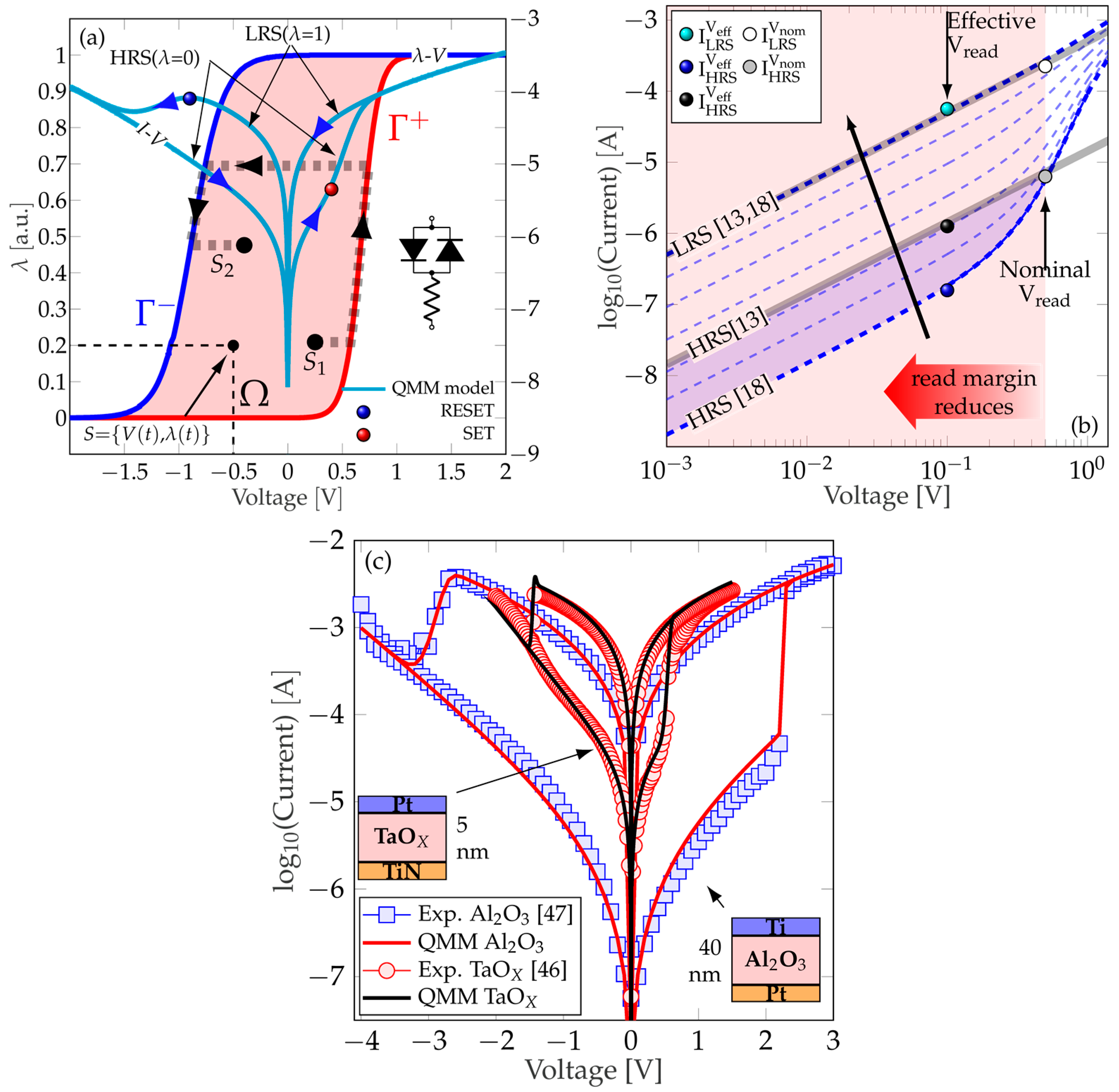
2. Quasi-Static Memdiode Model

The resistive switching (RS) mechanism is the fundamental phenomenon behind RRAM devices. In the particular cases of CBRAMs and OxRAMs, RS relies on the displacement of metal ions/oxygen vacancies within the dielectric film in a metal–insulator–metal (MIM) structure originated from the application of an external electrical stimulus, current or voltage [41,42,43,44]. Such migration of ions causes the alternate completion and destruction of a conductive filament (CF) spanning across the insulating film. For a ruptured CF, the device is in the high resistance state (HRS), often characterized by an exponential I-V relationship, while the completion of the CF leads to the low resistance state (LRS), which often exhibits a linear I-V curve [45,46]. In between these two extreme situations, the modulation of the CF transport properties renders intermediate states by voltage-controlled redox reactions. From the modeling viewpoint, the compact model originally proposed by Miranda in [18] and later extended by Patterson et al. in [19] is able to describe the major and minor I-V loops and the gradual transitions in bipolar resistive switches. This is accomplished, as shown in the inset of Figure 2a, by considering a nonlinear transport equation based on two identical opposite-biased diodes in series with a resistor. The I-V relationship resembles a diode with memory and that is why this device was termed memdiode. Notice that the antiparallel connected diodes allow the bidirectional current flow through the memdiode device, as for both positive and negative polarities there will be a forward biased diode. For the sake of completeness, the QMM is succinctly reviewed in the next paragraphs.
Physically, the memdiode is associated with a potential barrier that controls the electron flow in the CF. The conduction properties of this nonlinear device change according to the variation of this barrier. Due to the uncertainty in the area of the CF, instead of the potential barrier height, the diode current amplitude is used as the reference variable. Following Chua’s memristive device theory, the proposed model comprises two equations, one for the electron transport and a second equation for the memory state of the device (ME), which is controlled by a hysteresis operator. The equation for the I-V characteristic of a memdiode is given by the expression:
I = s g n ( V ) { W ( α R I 0 ( λ ) e α ( a b s ( V ) + R I 0 ( λ ) ) ) α R I 0 ( λ ) }
where I0(λ) = Imin(1 − λ) + Imaxλ is the diode current amplitude, α a fitting constant, and R a series resistance. Equation (1) is the solution of a diode with series resistance and W is the Lambert function. Imin and Imax are the minimum and maximum values of the current amplitude, respectively. abs(V) is the absolute value of the applied bias and sgn() the sign function. As I0 increases in Equation (1), the I-V curve changes its shape from exponential to linear through a continuum of states as experimentally observed for this kind of device. λ is a control parameter that runs between 0 (HRS) and 1 (LRS) and is given by the recursive operator (Equation (2)):
λ ( V ) = m i n { Γ ( V ) , m a x [ λ ( V ) , Γ + ( V ) ] }
where min() and max() are the minimum and maximum functions, respectively, and V is the voltage a timestep before V. The positive and negative ridge functions in Equation (2), Γ+(V) and Γ(V) represent the transitions from HRS to LRS (SET) and vice versa (RESET) and can be physically linked to the completion and destruction of the CF [45,46], respectively. They are defined by Equations (3) and (4)
Γ + ( V ) = { 1 + e η + ( V V + ) } 1
Γ ( V ) = { 1 + e η ( V V ) } 1
where η+ and η are the transition rates and V+ and V the threshold voltages for SET and RESET, respectively. λ(V) defines the so-called logistic hysteron or memory map of the device and keeps track of the history of the device as a function of the applied voltage (see Figure 2a). λ calculated from Equation (2) yields the transition from HRS to LRS and vice versa through a change in the properties of the diodes depicted in the inset of Figure 2a. The combination of Equations (1) and (2) results in a I-V loop such as that superimposed to the hysteron loop in Figure 2a, which starts in HRS (λ = 0) and evolves as indicated by the blue arrows. The name quasi-static comes from the fact that the characteristic time of the ions/vacancies responsible of the switching phenomenon is assumed to be infinite for a state within the hysteron structure. This implies that for a state located inside the hysteron loop no changes occur in the conduction characteristics, unless it reaches the ridge functions Γ+(V) or Γ(V). The QMM can be transformed into a dynamic model by incorporating the time module described in [19].
Figure 2b shows the HRS (exponential) to LRS (linear) transition, altogether with some intermediate states (solid blue lines). Note that the memdiode model can successfully describe both HRS and LRS curves by solely changing a single parameter in the transport equation. As λ is swept from 10 7 to 1, I0 in Equation (1) varies between I m i n and I m a x , causing the I-V curve to gradually change its shape from linear-exponential (HRS regime) to linear (LRS regime). This is a consequence of the potential drop in the series resistance which linearizes the transport equation. In a neuromorphic application such as the one discussed in this paper, the intermediate conductance states are achieved by means of a Write–Verify iterative loop approach. In such method, pulses of incremental amplitude are applied to the devices (Write) until the required conductance is reached (Verify) [17,38]. If the target conductance is exceeded, then increasing pulses with the opposite polarity are applied in a similar fashion to gradually reduce the conductance value (within an error margin). This writing methodology implies a transition as the one depicted in Figure 2a by the red-thick faded line, where the incremental pulses cause the system to evolve from the initial state S1 up to the final state S2 following Γ+. If the conductance target is exceeded, then the system moves down along Γ by the application of voltage pulses with the appropriate polarity. Another relevant feature of the proposed model is that it can be described by a simple SPICE script as shown in [17]. Finally, the accuracy of the model is reported in Figure 2c by fitting experimental data extracted from different published works. In particular, results obtained for Al2O3 [47] and TaOx [46] structures at room temperature under DC voltage sweeps are presented. In summary, the proposed QMM not only provides a simple SPICE-compatible implementation for the resistive memory devices but also a versatile one, as it can accurately fit the major and minor I-V loops measured in a wide variety of RRAM devices

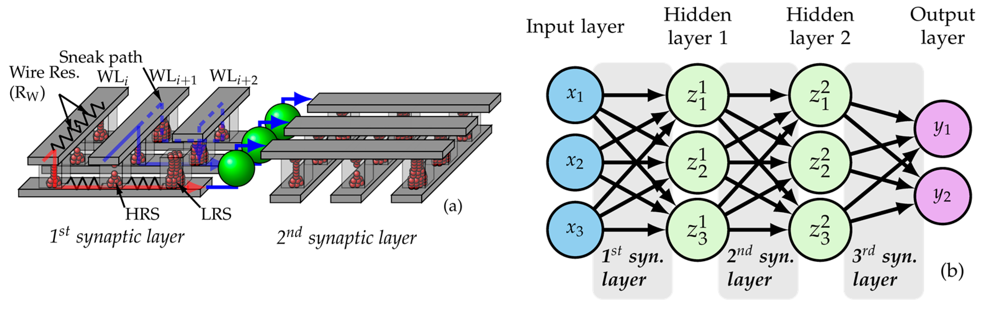
3. MCA-Based MLP Modeling and RL Calibration

Based on the procedure previously reported in [17] to create and simulate realistic circuital MCA-based SLPs intended for large dataset pattern recognition tasks, a novel procedure is derived here to account for a more practical case such as the MLP. For simplicity, ex-situ (off-line) supervised learning will remain as the training method of choice. To evaluate the MLP performance, the recognition of patterns from the MNIST [40] database (see Figure 3a,b) will be considered. Besides the extension to MLP classifiers, this modified workflow also involves an iterative calibration algorithm intended to minimize the RL-induced degradation of the inference accuracy. The chart depicted in Figure 3c summarizes the workflow. The tasks can be split into three parts: the first one comprises a set of MATLAB subroutines for creating, training, and writing the SPICE netlist for an ideal feed-forward MLP. The second part creates an idealized fully linear model of the MCA-based artificial neural networks (ANNs) in Python to calibrate the synaptic weights obtained during the training to account for the parasitic line resistances (the details can be seen in Figure 3d). Last but not least, the third part relates to the SPICE simulation of the proposed circuit during the inference phase.

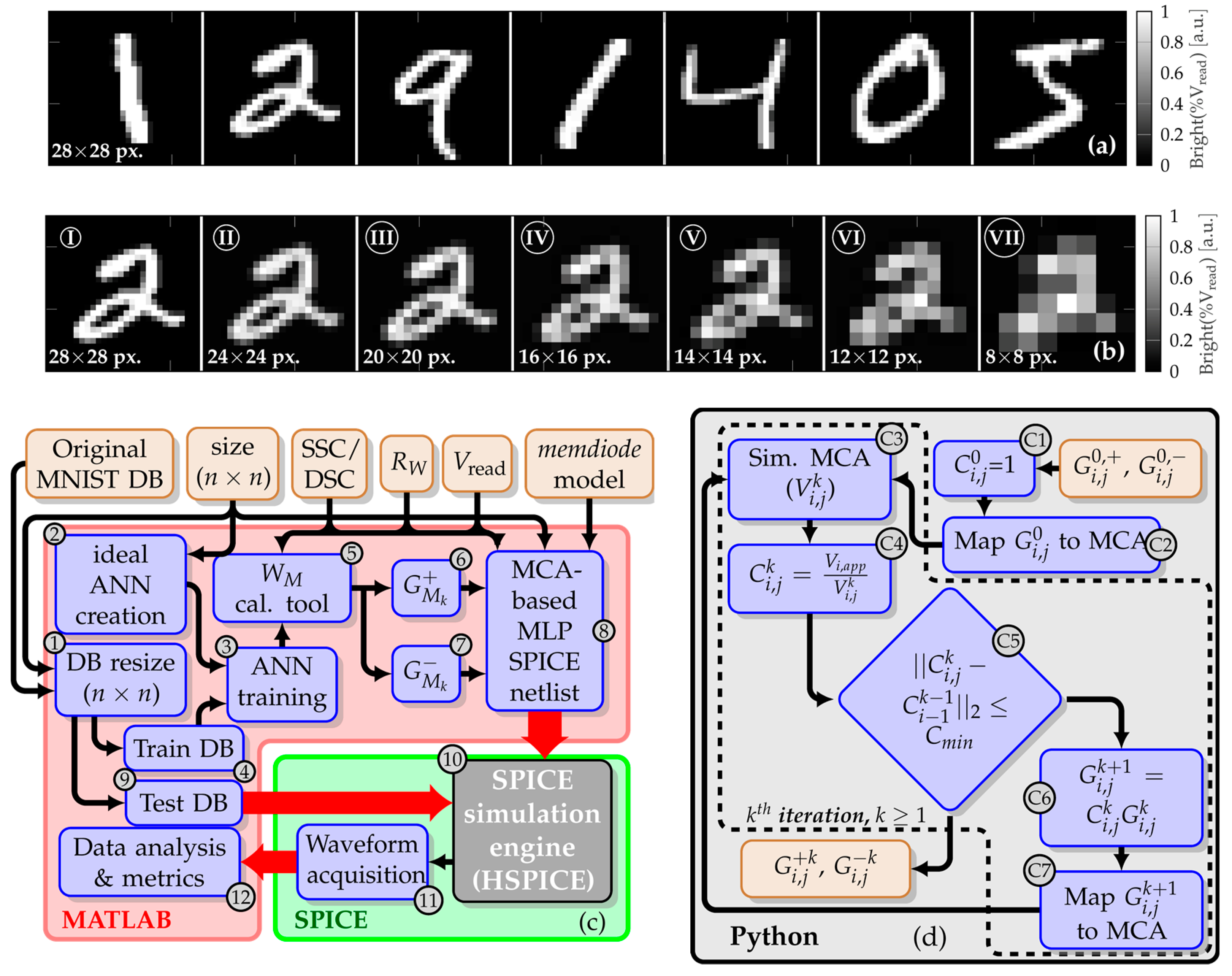
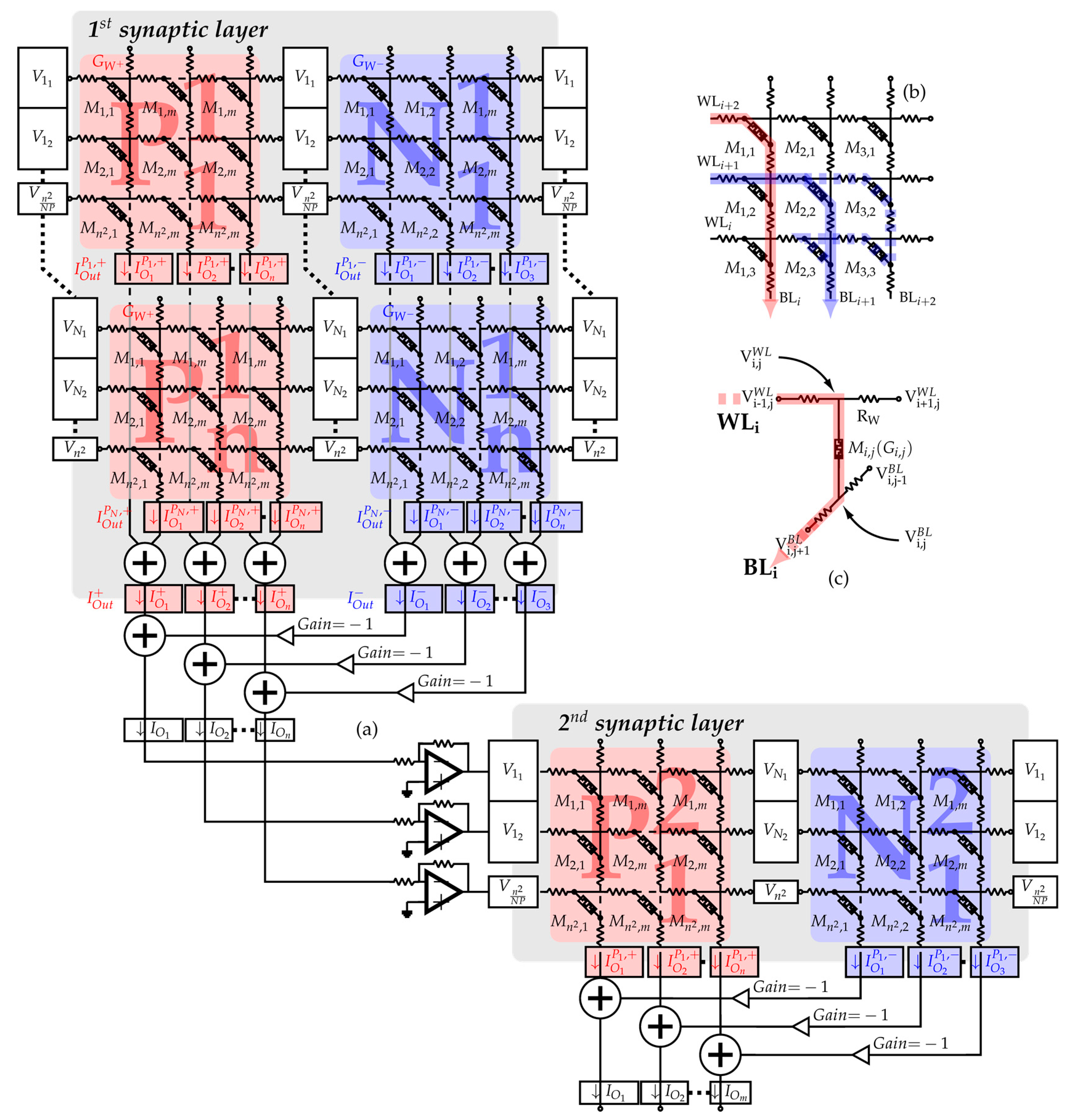
3.1. Simulation Flow

Regarding the MATLAB-implemented part of the procedure, the first step consists in creating the image (n × n pixels) database. This includes rescaling each image of the original database (item (1) in the flowchart shown in Figure 3c). The MNIST (Modified National Institute of Standards and Technology) is a large database of handwritten digits from 0 to 9 commonly used for training and testing image processing systems including ANNs in the field of machine learning. This database contains 60,000 training images and 10,000 testing images, both in grayscale and with a 28 × 28 pixels resolution [40]. A few examples of these images can be seen in Figure 3a where the x and y axes stand for the pixel index. Pixel brightness is codified into 256 gray levels between 0 (fully OFF, black) and 1 (fully ON, white). Resizing to different resolutions can be seen in Figure 3b.
Then, a software-based SLP or MLP with n2 inputs, 10 outputs and a number N of hidden neural layers (each of them comprising mi neurons) is created (2) and trained (3) using the previously rescaled database of training images (4). The MLP (or SLP) is ex-situ trained considering the scaled conjugate gradient (SCG) [48] as the training algorithm, as proposed in [17]. Further details concerning the training function are beyond the scope of this work, as we focus on the MCA-based implementation of the MLP. This produces N + 1 weight matrices W M k , with k ∈ {1, 2, …, N + 1} (5) (for instance for two hidden layers with m1 and m2 neurons each, three weight matrices W M 1 , W M 2 and W M 3 are obtained, with sizes n2 × m1, m1 × m2 and m2 × 10, respectively). To allow rendering both the positive and negative elements of W M k with the always positive conductance of the MCA, each synaptic weight is implemented using two memdiodes as suggested in [49,50,51] resulting in two MCAs per synaptic layer. Thereby, each W M K matrix is split into two matrices W M k + and W M k as:
w M k i , j + = { w M k i , j , w M i , j > 0 0 , w M i , j 0
w M k i , j = { w M k i , j , w M i , j < 0 0 , w M i , j 0
each of them containing only positive weights, so that W M K = W M k + W M k . In the next step, the conductance matrices G M k + and G M k ((6) and(7)) to be mapped onto the MCAs are calculated by the linear transformation [52]:
G M + , = G m a x G m i n m a x { W M k } m i n { W M k } W M k + , + [ G m a x ( G m a x G m i n ) m a x { W M k } m a x { W M k } m i n { W M k } ]
where [ G m i n , G m a x ] is a selected conductance range for a linear computation in matrix-vector calculations. For simplicity, we consider G m a x = G L R S = 1 R O N and G m i n = G H R S = 1 R O F F , where m a x { W M K } and m i n { W M K } are the maximum and minimum synaptic weight values in the software obtained W M K . In this way, the synaptic weights in the W M k + and W M k matrices are converted to conductance values within the range [ G H R S , G L R S ].
The subsequent subroutines generate the circuit netlist for the dual- n 2 x   m i , m i   x   m i + 1 , …, m N × 10 memdiode MCA-based MLP (8), adding the parasitic wire resistance, connection scheme, and control logic necessary to perform the inference phase. As reported in [17], a single MCA is not efficient for implementing large matrices. Given that both RL and RON/ROFF are normally defined by the selected fabrication node and RS mechanism, respectively, a widely accepted [51,53] alternative design consists of dividing the large matrices into smaller partitions, whose reduced size improves the voltage effectively delivered to the memristive cell. Figure 4a shows the simplified circuit schematic of the partitioned MCA and the interconnections required to realize the complete matrix-vector multiplication (MVM) in the 1st synaptic layer. Exploding the integrability of the MCA with CMOS circuitry, vertical interconnects used to connect the outputs of the vertical MCA partitions may be placed under the partitioned structure, as well as the analogue sensing electronics, allowing the partitioned MCA to maintain a similar area consumption than the original nonpartitioned case [51]. The vertical interconnects are grounded through the sensing circuit to absorb the currents within the same vertical wire.
Each memdiode in the MCAs is set to the corresponding conductance value from the G M k + and G M k matrices by adjusting the control parameter λ . The required value of λ is obtained by solving Equation (1), I = g k 1 , j + ( ) V , g k 1 , j + ( ) being each of the elements of G M k + ( G M k ). As in this work we focus on the artificial synapses modeling using the memdiode model, hidden neurons in the kth hidden neural layer connecting the two adjacent layers of synapses k − 1 and k + 1 are implemented in terms of a behavioral SPICE model. The model for each neuron involves a trans-impedance amplifier (TIA) that translates the output current in the associated bitline on the i − 1 synaptic layer to a voltage which is fed to a nonlinear activation function and then propagated to the corresponding wordline in the i + 1 synaptic layer. In this paper, we consider a log-sigmoidal (1/(1 + e−x)) activation function, though a tan-sigmoidal activation function could be used as well. The input stimulus in each synaptic layer is delivered following a dual side connection (DSC) scheme, as shown in the simplified equivalent circuit in Figure 4a. Despite the increased peripheral circuitry complexity, this scheme improves the voltage delivery to each synapse [10] by connecting the two wordline terminals to the same input stimuli. The input stimuli of the 1st synaptic layer is obtained by unrolling each of the rescaled grayscale n × n images of the test database (9) into an equivalent n2 × 1 vector and scaling it by a voltage V r e a d . V r e a d is chosen such as to prevent altering the memdiode states during the inference simulation. In this way, during the inference process each of the test images is presented to the MLP as a vector of analogue voltages in the range [0, Vread]. Once the circuit netlist has been generated, it is passed to the HSPICE simulator (10) which evaluates the voltage and current distributions in the MCA-based MLP circuit while it processes and classifies the input images (11) and then passes the resulting waveforms back to the MATLAB routine for metrics extraction (12).

3.2. Calibration Tool Workflow

In an ideal case scenario, that is with RL negligible, the output current for a column (or bitline) in a MCA of the kth synaptic layer of a MLP or SLP is given by Equation (8), where the g k i , j + ( ) elements are the junction conductances along one bitline and V k i , a p p the wordline voltages. Note that the voltage applied to each artificial synapse (conductances) is independent of the device location within the MCA provided that no voltage drops occur in the interconnection lines. Instead, in a real case scenario, the voltage applied across each junction depends on the device location in the MCA partition as indicated by Equation (9). This happens because a significant IR-drop occurs in the line resistances. Consequently, the voltage applied across each junction is always lower than the applied wordline voltage, and so it is the resulting output current I r e a l k j
I i d e a l j k + ( ) = g k 1 , j + ( ) V k 1 , a p p + g k 2 , j + ( ) V k 2 , a p p + g k 3 , j + ( ) V k 3 , a p p + + g k N , j + ( ) V k 1 , a p p
I r e a l j k + ( ) = g k 1 , j + ( ) V k 1 , j + g k 2 , j + ( ) V k 2 , j + g k 3 , j + ( ) V k 3 , j + + g k N , j + ( ) V k 1 , j
An interesting approach to compensate for the smaller currents was presented by Lee et al. in [13]. In their study, the authors propose to increase the conductance level of each individual memory cell proportionally to the voltage reduction. Let us then consider a calibration factor c k i , j + ( ) = V k i , a p p V k i , j 1 for each element in the MCA. Then the compensated conductance of each memristive device is calculated as g k i , j + ( ) = g k i , j + ( ) c k i , j + ( ) . Since the calibrated conductances ( g k i , j + ( ) ) are higher than the previous ones ( g k i , j + ( ) ), the overall current increases and consequently so does the IR-drops along the word and bitlines. Thereby, this method implies multiple iterations until convergence is reached.
To speed-up the iterative calibration process, a parametric fully linear model of the MCA-based MLP was developed. In this scenario each memristor is represented as a resistor of fixed value and the overall MCA model (see Figure 4b) is expressed in terms of a system of coupled equations arising from considering the Current Kirchhoff Law at each junction of the MCA (see Figure 4c). The details of such modeling approach first considered in [10] are included in Appendix A. This method avoids calculating the required values of λ for each memdiode in each iteration, which significantly reduces the calibration time, especially for large networks. The simulation code was implemented in Python, taking advantage of the object oriented programming characteristic of such language. In this context, each MCA in a partitioned multilayer perceptron can be easily created as an instance of a unique class that describes the properties and behavior of a single MCA.
The details of the iterative calibration process (block (5) in the flowchart of Figure 3c) are illustrated in Figure 3d and Algorithm 1. First, the synaptic weight matrices W M K , delivered from the training process (block (4) in the flowchart of Figure 3c) are mapped onto each MCA of the complete MLP (block (C2) in the flowchart of Figure 3d). The input stimuli feed to each MCA during calibration consists of a vector of analogue voltages obtained from averaging the brightness of each pixel from the images of the training set (C3). By solving the system of coupled equations, the effective voltage delivered to each memristor is calculated and used to compute the required calibration factor c k i , j + ( ) = V k i , a p p V k i , j (C4). Then, the absolute distances to the values calculated in the previous loop are compared against a predefined target, which represents a termination criterion for the process (C5). If the distance to the target exceeds the criterion, the conductance matrices are calculated as g k i , j + ( ) = g k i , j + ( ) c k i , j + ( ) (C6) and remapped onto the MCA object (C7) and the voltages at the nodes recalculated (C3). The iterative loop from (C3)–(C7) is then repeated until the termination criterion is met. The results of this iterative calibration process are the 2k matrices of calibrated conductance values G M k + , G M k , (blocks (6) and (7) in the flowchart of Figure 3c).
Algorithm 1: Iterative calibration algorithm
Jlpea 11 00009 i001

4. Simulation Results and Discussion

The line resistance between adjacent cells can be calculated as RL = ρ · L/(W · T), where L and W are the wire length between adjacent cells and wire width, respectively. For simplicity, they are taken equal to the feature size F. T is the metal thickness which is assumed >10 nm. In this context, RL ranges from 1 to 10 Ω, as the resistivity of conventional metal wires (ρ) ranges from 10−8 to 10−7 Ω·m. Thereby, RL can be estimated to be ≈4.53, 2.97, and 1.55 Ω for the 16, 22, and 32 nm technology nodes, respectively [13]. However, in Cu-wires there is a non-negligible size-dependent resistivity for technology nodes below the 10 nm limit, caused by the surface and grain boundary scattering as the mean free path of electrons becomes comparable to the wire dimensions. According to the Fuchs–Sondheimer (FS) and the Mayadas–Shatzkes (MS) models [53], RL for highly scaled nodes can be as large as ≈100 kΩ. Considering the QMM model, the influence of the line resistance is evaluated in the following Section 4.1 and Section 4.2, assuming a different number of hidden layers and two alternative approaches to minimize the parasitic voltage drop, respectively.

4.1. Influence of the Number of Hidden Layers

Unlike the case of SLP, where the network size (in terms of the number of devices) is fixed by the pattern features and possible output classes, in case of MLP, the introduction of hidden neural layers results in multiple possible networks for the classification of a given pattern dataset [54]. In this regard, it is known that as the number of hidden layers increases, so does the overall network accuracy. Nevertheless, when considering a realistic memristor-based implementation as done in this paper, there is a degradation of the signals propagated across each synaptic layer due to the line resistance in combination with the sneakpath effect. Consequently, the hidden neurons are prone to propagate erroneous signals, thus threatening the accuracy of the MLP. To shed light on this issue, five MLPs comprising different numbers of hidden layers and neurons per layer were simulated. The obtained results are summarized in Table 1, considering for all cases the MNIST images resized to 8 × 8 px, dual-side-connection, no partitioning of the MCA used for each synaptic layer, Vread = 300 mV and RL swept from 100 mΩ to 1 kΩ. The synaptic connections are modeled with the QMM SPICE subcircuit described in [17] and considering the following set of parameters: Imin = 85 nA, Imax = 52 µA, αmin = 4.5, αmax = 2.5, Rmin = Rmin = 110 Ω, and β = 0.5. This combination of values renders (at the nominal Vread) resistances ROFF ≈ 577 kΩ and RON ≈ 7.5 kΩ (approx. an ROFF/RON ratio in the order of 100).
The simulation results are graphically reported in Figure 5, where the inference accuracy as function of RL is shown normalized against the inference accuracy for RL→0 Ω. A central point to highlight here is the notorious increase of the MLP sensitivity to RL when compared against the reference SLP, regardless of the number of hidden layers and neurons per layer. This could be explained by taking into account the larger size of the synaptic layers involved for the MLPs cases (the MCAs used for the SLP has a maximum size of 64 × 10 while for the MLP-#a it increases up to 64 × 54). The use of larger MCAs with no partitions to implement the synaptic connections degrades the effective voltage delivered to the synapses located away from the driving ports of the MCA. The ratio between the effective voltage delivered to each synapse and the nominal applied voltage is known as the read margin, and it has been shown in [17] that for a given value of RL, it decreases as the size of the MCA grows, directly degrading the inference accuracy. This interpretation is also supported by the results obtained for the set of MLPs named MLP-#b. For these simulations, the RL sensitivity further increases as it could be expected given the bigger size of the largest MCA involved in the network (64 × 100 for the set MLP-#b against 64 × 54 for MLP-#a). It is also worth noting that both the MLP-#a and MLP-#b sets follow unique decreasing trends with RL regardless of the number of layers. Thereby the increase in the number of hidden layers does not significantly compromise the RL sensitivity but allows a non-negligible increase in the inference accuracy, as shown in the inset of Figure 5. Instead, the number of neurons per layer causes a sensible increase of the inference accuracy degradation caused by RL, as it implies changes in the MCAs used to implement the MLP.

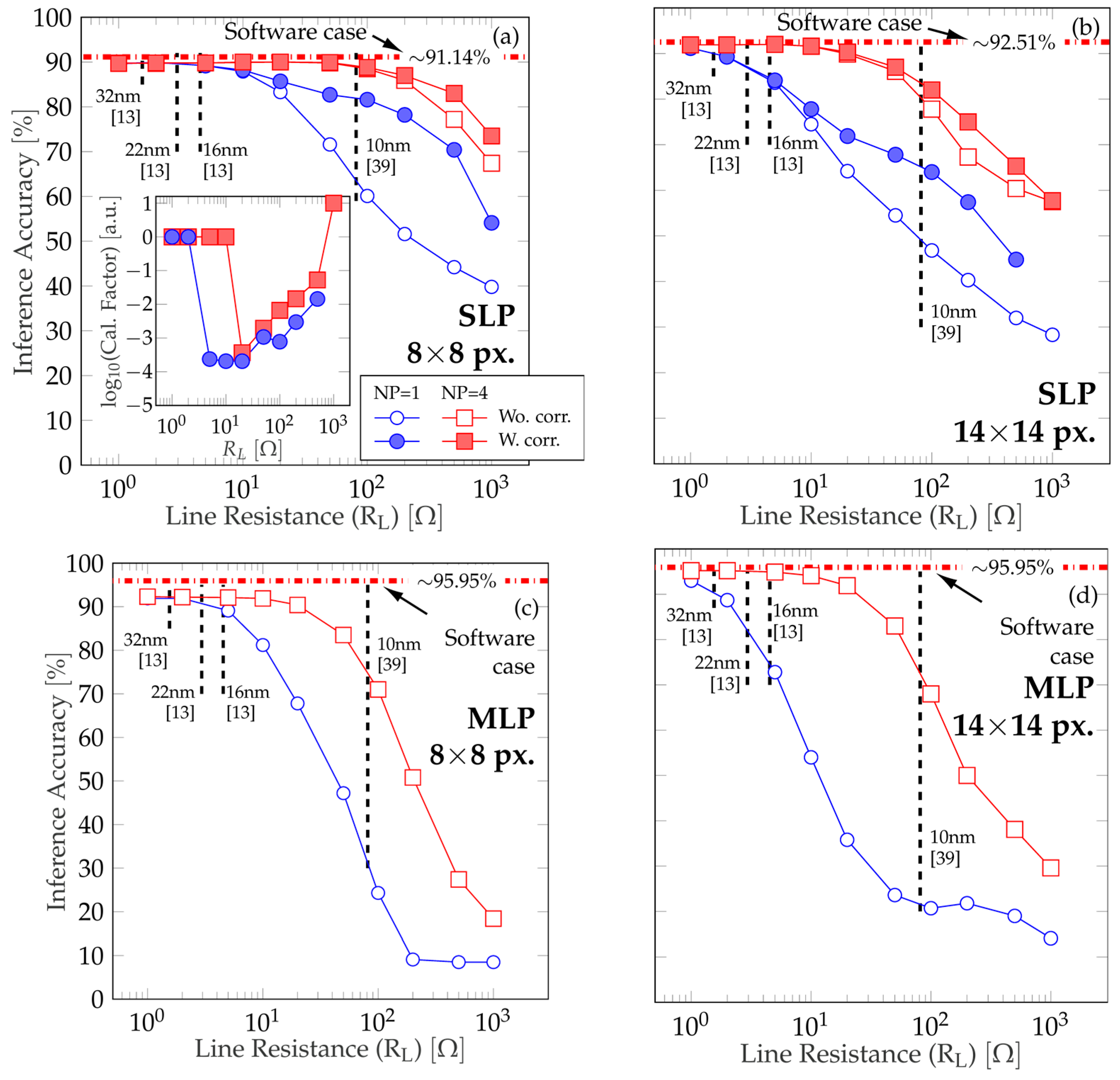
4.2. Techniques to Minimize the Impact of the Line Resistance (RL)

As mentioned in the previous subsection, the voltage drop occurring across the parasitic line resistances imposes a serious limitation to the number of neurons that can be included in each neural layer without causing a major reduction of the inference accuracy. Methods to minimize this problem are thereby mandatory to allow rendering MLPs capable of dealing with large input patterns. For instance, in [55], Truong et al. proposed a circuit to compensate the voltage drop across the interconnections. Although capable of improving the inference metrics, the proposed method implies a significant circuit overhead and might be not suitable for networks involving a large number of neurons. Therefore, the search for alternative solutions requiring lesser additional circuitry is encouraged. Two of them were discussed in Section 3.1 and Section 3.2, namely the MCA partitioning and the iterative calibration of the synaptic weights. Although tested in [13,17], their applicability in MLP has not yet been addressed considering realistic electrical simulations. Thus, in this section the capability of such techniques to mitigate the line resistance impact on MLP is studied based on the framework defined in Section 3.1 and using the same values for the QMM as in Section 4.1. Only one hidden layer is considered as it was shown in Section 4.1 that the number of layers does not significantly alter the RL dependency. Instead two different MNIST representation sizes are considered: 8 × 8 px. (64 × 54 × 10 as reported in [9]) and 14 × 14 px. (196 × 20 × 10 as reported in [38]) to account for the MCA size dependency. For comparison purposes we also report the case of pattern classification with SLPs (of sizes 64 × 10 and 196 × 10).
Let us first consider the nonpartitioned (NP = 1), uncalibrated cases (blue empty markers). As it can be seen in Figure 6, in all cases (MLP and SLP for 8 × 8 px. and 14 × 14 px. images) the inference accuracy approaches the ideal case as RL tends to zero. Nonetheless, when considering the 14 × 14 px. images (Figure 6b,d) a higher accuracy degradation is observed, as expected for the use of a larger MCA as the first synaptic layer. This can be seen as a left-shift of the accuracy vs. RL curves when the image size is increased and occurs both for the SLP (see the displacement of the trend from Figure 6a,b) and the MLP (Figure 6c,d) cases. Note that for the 14 × 14 px. images there is a significant accuracy loss even for low values of the line resistance (see Figure 6d for instance, where a value of RL of approx. 5 Ω obtained for a feature size of 16 nm causes the inference accuracy to drop from approx. 96% to 73%). It is also worth mentioning that the steeper decrease of the inference accuracy vs. RL observed in MLPs vs. SLP trained to classify the 8 × 8 px. images in Figure 5 is also present for the 14 × 14 px. images (see Figure 6b,d).
To improve the metrics discussed in the previous paragraph, the post-training iterative calibration of the synaptic weights is first performed on the nonpartitioned SLP (filled blue lines). This process has two different outcomes: on one hand when considering the SLP case, a clear improvement of up to approx. 30% for the 8 × 8 px images (Figure 6a) can be observed for RL values approaching 100 Ω in highly scaled fabrication nodes [53]. Beyond this limit, the capability of the calibration method to reduce the voltage drop in the interconnections is not enough and thereby the accuracy improvement becomes smaller. A very similar behavior is shown in Figure 6b for the 14 × 14 px images. However, given the larger size of the MCAs involved, the improvement is smaller (not bigger than 20%). As the target calibration factor passed to the calibration routine is defined by the user, in this paper we performed an iterative loop to automatically determine the calibration factor that allows maximizing the inference accuracy. The resulting factors are plotted against the inference accuracy in the inset of Figure 6a for the 8 × 8 px. images. Note that for low RL values, the calibration factor plays no role as no calibration is indeed required (the parasitic voltage drop due to the line resistance is negligible). Then the factor is tightened and progressively relaxed as the line resistance increases, as if the calibration factor is too exigent the calibration cannot yield a real accuracy improvement.
When addressing the case of the MLPs with different sizes, it was found that the calibration process produces a marginal improvement, resulting in identical inference vs. RL trends as in the noncalibrated cases (and thereby not plotted in Figure 6c,d as they would coincide with the noncalibrated trends). Instead, the use of partitioned schemes for the realization of the complete MCA-based synaptic layers is shown to be efficient both for SLPs and MLPs. For instance, when the 64 × 10 SLP shown in Figure 6a is partitioned into four blocks of 16 × 10 the inference accuracy notably increases (note the empty red markers). The same effect is observed for the 196 × 10 MCA (partitioned into four blocks of 49 × 10) from which the results presented in Figure 6b were extracted. Furthermore, the inference accuracy of the partitioned SLP can also be improved by using the calibration algorithm (filled red markers in Figure 6a,b). For the MLP, the enhancement achieved with the partitioning is seen as a right shift in the accuracy vs. RL trends. Note that in these cases, the first layer in the 64 × 54 × 10 MLP (Figure 6c) was implemented with 12 blocks of 16 × 18 and the second layer with three blocks of 18 × 10 and for the 196 × 20 × 10 MLP (Figure 6d), the first layer was implemented using four partitions of 49 × 20 and the second layer was not partitioned (20 × 10).

5. Conclusions

In this paper we extended the use of the Quasi-static Memdiode Model (QMM) previously proven for single-layer perceptrons (SLPs) to the SPICE modeling and simulation of multilayer perceptrons (MLPs) intended for large dataset pattern recognition. The versatility and reduced computational cost of this model allow performing electrical simulations without losing accuracy. The inference performance was tested considering the MNIST dataset of grey-scale handwritten digits, rescaled to different resolutions to test MLPs of different sizes. Two aspects were analyzed: the impact of the MLP structure (number of layers and neurons per layer) on the inference accuracy and alternative techniques to mitigate the impact of the line resistance. Concerning the first point, it was found that the number of hidden layers does not cause major variations in the line resistance dependence of the inference accuracy. Instead, it is the size of the largest synaptic layer what acts as a bottleneck, severely limiting the overall accuracy. Thereby the addition of memristive-based synaptic layers helps improving the accuracy without inducing further RL-related degradation. Concerning the second point, the use of partitioned schemes was shown to provide the best performance results both in SLP and MLP when compared to the calibration technique. In fact, the calibration technique resulted in no gain in terms of accuracy when applied to MLP networks. This should be taken into account by circuit designers.

Author Contributions

Conceptualization, F.L.A. and E.M.; methodology, F.L.A., N.M.G. and E.M.; software, F.L.A., N.M.G. and E.M.; validation, F.L.A., N.M.G., S.M.P., F.P., J.S. E.M.; formal analysis, F.L.A., E.M.; investigation, F.L.A., N.M.G., S.M.P., F.P., J.S. E.M.; resources, F.P, J.S and E.M.; data curation, F.L.A.; writing—original draft preparation, F.L.A., N.M.G. and E.M.; writing—review and editing, F.L.A., N.M.G., S.M.P., F.P., J.S. and E.M.; visualization, F.A, E.M.; supervision, E.M.; project administration, F.P., J.S. and E.M; funding acquisition, F.P., J.S. and E.M. All authors have read and agreed to the published version of the manuscript.

Funding

This research has been funded by both Argentinean and European institutions. Argentine funding was provided by MINCyT (Contracts PICT2013/1210, PICT 2016/0579 and PME 2015-0196), CONICET (Project PIP-11220130100077CO) and UTN.BA (Projects PID-UTN EIUTIBA4395TC3, CCUTIBA4764TC, MATUNBA4936, CCUTNBA5182 and CCUTNBA6615). E.M. and J. S. acknowledge the support from TEC2017-84321-C4-4-R and WAKeMeUP 783176 projects, cofunded by grants from the Spanish Ministerio de Ciencia e Innovación and the ECSEL-EU Joint Undertaking.

Conflicts of Interest

The authors declare no conflict of interest.

Appendix A

Each MCA is described using the equivalent circuit schematic represented in Figure 4b, by considering the 2nd Kirchhoff’s law on the terminals of each memristive device (see Figure 4c), which will have the form of any of the Equations (A1)–(A6) depending on the device location within the MCA. GL is the line conductance (1/RL), G i , i n B L = G i , i n W L are the wordline and bitline access conductances (resistance in the BL/WL terminals) ( G i , i n W L = 1 / R i , i n W L and G i , i n B L = 1 / R i , i n B L ), V i , a p p W L are the applied voltages in the WL terminals, corresponding to the MNIST images and V j , a p p B L are grounded through a sensing resistor. Node voltages in the WLs are indicated as V i , j W L and, in the same way, V i , j B L refers to node voltages in the BLs. Six different equations arise as they account for the elements located at the BL/WL terminals (Equations (A2), (A3), (A5) and A6) or somewhere in between (Equations (A1) and (A4)).
( W L , ( i , j ) ) : G L ( V i , j W L V i , i 1 W L ) G i , j ( V i , j B L V i , i W L ) G L ( V i , j + 1 W L V i , j W L ) = 0
( W L , j = 1 ) : G i , i n W L ( V i , 1 W L V i , a p p W L ) G i , j ( V i , 1 B L V i , 1 W L ) G L ( V i , 2 W L V i , 1 W L ) = 0
( W L , j = n ) : G L ( V i , n W L V i , n 1 W L ) G i , n ( V i , n B L V i , n W L ) = 0
( B L , ( i , j ) ) : G L ( V i + 1 , j B L V i , i B L ) G i , j ( V i , j B L V i , j W L ) G L ( V i , j B L V i 1 , j B L ) = 0
( B L ,   i = m ) : G i n , j B L ( V i , j W L V i , i 1 W L ) G i , j ( V i , j B L V i , i W L ) G L ( V i , j + 1 B L V i , j B L ) = 0
( B L , i = 1 ) : G L ( V 2 , j B L V 1 , j B L ) G i , j ( V 1 , j B L V 1 , j W L ) = 0
This results in a system of 2 mn coupled equations, with 2mn unknown voltages corresponding to the WL ( V W L = [ V 1 , 1 W L , V 1 , 2 W L , , V 1 , n W L , V 2 , 1 W L , , V n , m W L ] T ) and BL ( V B L = [ V 1 , 1 B L , V 1 , 2 B L , , V 1 , n B L , V 2 , 1 B L , , V n , m B L ] T ) voltages. By defining the column vectors EWL and EBL as [ G 1 , i n W L V 1 , i n W L , 0 , , G 2 , i n W L V 2 , i n W L , 0 , , G m , i n W L V m , i n W L ] and [ G 1 , i n B L V 1 , i n B L , 0 , , G 2 , i n B L V 2 , i n B L , 0 , , G n , i n B L V n , i n B L ] respectively, Equations (A1)–(A6) can be represented following a matrix formulation as in Equation (A7):
[ A B C D ] [ V W L V B L ] = [ E W L E B L ]
where all A, B, C, and D matrix are m × n. Further details regarding the structure of these matrices can be found in [10]. Then the output of the m × n MCA is a row vector of 1 × n currents, defined as I O u t = V n , j B L G L , with 1 j m , obtained by solving Equation (A7). It should be noted that the system of coupled equations presented in the matrix formulation of Equation (A7) allow representing both the case of the input voltage being applied from one single side or from both sides of WLs.

References

  1. Li, C.; Belkin, D.; Li, Y.; Yan, P.; Hu, M.; Ge, N.; Jiang, H.; Montgomery, E.; Lin, P.; Wang, Z.; et al. In-Memory Computing with Memristor Arrays. In Proceedings of the 2018 IEEE International Memory Workshop (IMW), Kyoto, Japan, 13–16 May 2018; pp. 1–4. [Google Scholar]
  2. Upadhyay, N.K.; Joshi, S.; Yang, J.J. Synaptic electronics and neuromorphic computing. Sci. China Inf. Sci. 2016, 59, 1–26. [Google Scholar] [CrossRef] [Green Version]
  3. Sasago, Y.; Kinoshita, M.; Morikawa, T.; Kurotsuchi, K.; Hanzawa, S.; Mine, T.; Shima, A.; Fujisaki, Y.; Kume, H.; Moriya, H.; et al. Cross-Point Phase Change Memory with 4F2 Cell Size Driven by Low-Contact-Resistivity Poly-Si Diode. In Proceedings of the Digest of Technical Papers-Symposium on VLSI Technology, Kyoto, Japan, 16–18 June 2009; pp. 24–25. [Google Scholar]
  4. Truong, S.N.; Ham, S.-J.; Min, K.-S. Neuromorphic crossbar circuit with nanoscale filamentary-switching binary memristors for speech recognition. Nanoscale Res. Lett. 2014, 9, 629. [Google Scholar] [CrossRef] [PubMed] [Green Version]
  5. Truong, S.N.; Min, K.-S. New Memristor-Based Crossbar Array Architecture with 50-% Area Reduction and 48-% Power Saving for Matrix-Vector Multiplication of Analog Neuromorphic Computing. J. Semicond. Technol. Sci. 2014, 14, 356–363. [Google Scholar] [CrossRef]
  6. Truong, S.N.; Shin, S.; Byeon, S.-D.; Song, J.; Min, K.-S. New Twin Crossbar Architecture of Binary Memristors for Low-Power Image Recognition with Discrete Cosine Transform. IEEE Trans. Nanotechnol. 2015, 14, 1104–1111. [Google Scholar] [CrossRef]
  7. Hu, M.; Li, H.; Chen, Y.; Wu, Q.; Rose, G.S.; Linderman, R.W. Memristor Crossbar-Based Neuromorphic Computing System: A Case Study. IEEE Trans. Neural Netw. Learn. Syst. 2014, 25, 1864–1878. [Google Scholar] [CrossRef]
  8. Liu, B.; Li, H.; Chen, Y.; Li, X.; Huang, T.; Wu, Q.; Barnell, M. Reduction and IR-drop compensations techniques for reliable neuromorphic computing systems. In Proceedings of the 2014 IEEE/ACM International Conference on Computer-Aided Design (ICCAD), San Jose, CA, USA, 2–6 November 2014; pp. 63–70. [Google Scholar] [CrossRef]
  9. Li, C.; Belkin, D.; Li, Y.; Yan, P.; Hu, M.; Ge, N.; Jiang, H.; Montgomery, E.; Lin, P.; Wang, Z.; et al. Efficient and self-adaptive in-situ learning in multilayer memristor neural networks. Nat. Commun. 2018, 9, 1–8. [Google Scholar] [CrossRef] [Green Version]
  10. Chen, A. A Comprehensive Crossbar Array Model with Solutions for Line Resistance and Nonlinear Device Characteristics. IEEE Trans. Electron Devices 2013, 60, 1318–1326. [Google Scholar] [CrossRef]
  11. Park, S.; Kim, H.; Choo, M.; Noh, J.; Sheri, A.; Jung, S.; Seo, K.; Park, J.; Kim, S.; Lee, W.; et al. RRAM-based synapse for neuromorphic system with pattern recognition function. In Proceedings of the 2012 International Electron Devices Meeting, San Francisco, CL, USA, 10–13 December 2012; Institute of Electrical and Electronics Engineers (IEEE): New York, NY, USA, 2012; pp. 10.2.1–10.2.4. [Google Scholar]
  12. Ham, S.-J.; Mo, H.-S.; Min, K.-S. Low-Power VDD/3 Write Scheme with Inversion Coding Circuit for Complementary Memristor Array. IEEE Trans. Nanotechnol. 2013, 12, 851–857. [Google Scholar] [CrossRef]
  13. Lee, Y.K.; Jeon, J.W.; Park, E.-S.; Yoo, C.; Kim, W.; Ha, M.; Hwang, C.S. Matrix Mapping on Crossbar Memory Arrays with Resistive Interconnects and Its Use in In-Memory Compression of Biosignals. Micromachines 2019, 10, 306. [Google Scholar] [CrossRef] [Green Version]
  14. Han, R.; Huang, P.; Zhao, Y.; Cui, X.; Liu, X.; Jin-Feng, K. Efficient evaluation model including interconnect resistance effect for large scale RRAM crossbar array matrix computing. Sci. China Inf. Sci. 2018, 62, 22401. [Google Scholar] [CrossRef] [Green Version]
  15. Yakopcic, C.; Taha, T.M.; Subramanyam, G.; Pino, R.E. Memristor SPICE Modeling. In Advances in Neuromorphic Memristor Science and Applications; Springer Nature: London, UK, 2012; pp. 211–244. [Google Scholar]
  16. Yakopcic, C.; Hasan, R.; Taha, T.; McLean, M.; Palmer, D. Memristor-based neuron circuit and method for applying learning algorithm in SPICE. Electron. Lett. 2014, 50, 492–494. [Google Scholar] [CrossRef] [Green Version]
  17. Aguirre, F.L.; Pazos, S.M.; Palumbo, F.; Sune, J.; Miranda, E. Application of the Quasi-Static Memdiode Model in Cross-Point Arrays for Large Dataset Pattern Recognition. IEEE Access 2020, 8, 202174–202193. [Google Scholar] [CrossRef]
  18. Miranda, E. Compact Model for the Major and Minor Hysteretic I–V Loops in Nonlinear Memristive Devices. IEEE Trans. Nanotechnol. 2015, 14, 787–789. [Google Scholar] [CrossRef]
  19. Patterson, G.; Sune, J.; Miranda, E. Voltage-Driven Hysteresis Model for Resistive Switching: SPICE Modeling and Circuit Applications. IEEE Trans. Comput. Des. Integr. Circuits Syst. 2017, 36, 2044–2051. [Google Scholar] [CrossRef] [Green Version]
  20. Yakopcic, C.; Taha, T.M.; Subramanyam, G.; Pino, R.E. Generalized Memristive Device SPICE Model and its Application in Circuit Design. IEEE Trans. Comput. Des. Integr. Circuits Syst. 2013, 32, 1201–1214. [Google Scholar] [CrossRef]
  21. Kvatinsky, S.; Friedman, E.G.; Kolodny, A.; Weiser, U.C. TEAM: ThrEshold Adaptive Memristor Model. IEEE Trans. Circuits Syst. I Regul. Pap. 2013, 60, 211–221. [Google Scholar] [CrossRef]
  22. Kvatinsky, S.; Ramadan, M.; Friedman, E.G.; Kolodny, A. VTEAM: A General Model for Voltage-Controlled Memristors. IEEE Trans. Circuits Syst. II Express Briefs 2015, 62, 786–790. [Google Scholar] [CrossRef]
  23. Eshraghian, K.; Kavehei, O.; Cho, K.R.; Chappell, J.M.; Iqbal, A.; Al-Sarawi, S.F.; Abbott, D. Memristive device fundamentals and modeling: Applications to circuits and systems simulation. Proc. IEEE 2012, 100, 1991–2007. [Google Scholar] [CrossRef] [Green Version]
  24. Biolek, D.; Biolek, Z.; Biolková, V.; Kolka, Z. Modeling of TiO2 memristor: From analytic to numerical analyses. Semicond. Sci. Technol. 2014, 29, 125008. [Google Scholar] [CrossRef]
  25. Biolek, Z.; Biolek, D.; Biolkova, V.; Kolka, Z. Reliable Modeling of Ideal Generic Memristors via State-Space Transformation. Radioengineering 2015, 24, 393–407. [Google Scholar] [CrossRef]
  26. Kim, T.; Kim, H.; Kim, J.; Kim, J.-J. Input Voltage Mapping Optimized for Resistive Memory-Based Deep Neural Network Hardware. IEEE Electron Device Lett. 2017, 38, 1228–1231. [Google Scholar] [CrossRef]
  27. Choi, S.; Lee, J.; Kim, S.; Lu, W.D. Retention failure analysis of metal-oxide based resistive memory. Appl. Phys. Lett. 2014, 105, 113510. [Google Scholar] [CrossRef]
  28. Raghavan, N.; Frey, D.D.; Bosman, M.; Pey, K.L. Statistics of retention failure in the low resistance state for hafnium oxide RRAM using a Kinetic Monte Carlo approach. Microelectron. Reliab. 2015, 55, 1422–1426. [Google Scholar] [CrossRef]
  29. Lin, Y.-D.; Chen, P.S.; Lee, H.-Y.; Chen, Y.-S.; Rahaman, S.Z.; Tsai, K.-H.; Hsu, C.-H.; Chen, W.-S.; Wang, P.-H.; King, Y.-C.; et al. Retention Model of TaO/HfOX and TaO/AlOX RRAM with Self-Rectifying Switch Characteristics. Nanoscale Res. Lett. 2017, 12, 407. [Google Scholar] [CrossRef] [PubMed] [Green Version]
  30. Wong, H.S.P.; Lee, H.Y.; Yu, S.; Chen, Y.S.; Wu, Y.; Chen, P.S.; Lee, B.; Chen, F.T.; Tsai, M.J. Metal–oxide RRAM. Proc. IEEE 2012, 100, 1951–1970. [Google Scholar] [CrossRef]
  31. Wu, W.; Wu, H.; Gao, B.; Yao, P.; Zhang, X.; Peng, X.; Yu, S.; Qian, H. A methodology to improve linearity of analog RRAM for neuromorphic computing. In Proceedings of the IEEE Symposium on VLSI Technology, Honolulu, HI, USA, 18–22 June 2018; pp. 103–104. [Google Scholar]
  32. Kim, S.; Park, B.-G. Nonlinear and multilevel resistive switching memory in Ni/Si3N4/Al2O3/TiN structures. Appl. Phys. Lett. 2016, 108, 212103. [Google Scholar] [CrossRef]
  33. Ciprut, A.; Friedman, E.G. Energy-Efficient Write Scheme for Nonvolatile Resistive Crossbar Arrays with Selectors. IEEE Trans. Very Large Scale Integr. (VLSI) Syst. 2018, 26, 711–719. [Google Scholar] [CrossRef]
  34. Yao, P.; Wu, H.; Gao, B.; Tang, J.; Zhang, Q.; Zhang, W.; Yang, J.J.; Qian, H. Fully hardware-implemented memristor convolutional neural network. Nat. Cell Biol. 2020, 577, 641–646. [Google Scholar] [CrossRef]
  35. Wang, C.; Feng, D.; Tong, W.; Liu, J.; Li, Z.; Chang, J.; Zhang, Y.; Wu, B.; Xu, J.; Zhao, W.; et al. Cross-point Resistive Memory. ACM Trans. Des. Autom. Electron. Syst. 2019, 24, 1–37. [Google Scholar] [CrossRef]
  36. Chang, C.-C.; Chen, P.-C.; Chou, T.; Wang, I.-T.; Hudec, B.; Chang, C.-C.; Tsai, C.-M.; Chang, T.-S.; Hou, T.-H. Mitigating Asymmetric Nonlinear Weight Update Effects in Hardware Neural Network Based on Analog Resistive Synapse. IEEE J. Emerg. Sel. Top. Circuits Syst. 2018, 8, 116–124. [Google Scholar] [CrossRef]
  37. Wang, W.; Song, W.; Yao, P.; Li, Y.; Van Nostrand, J.; Qiu, Q.; Ielmini, D.; Yang, J.J. Integration and Co-design of Memristive Devices and Algorithms for Artificial Intelligence. iScience 2020, 23, 101809. [Google Scholar] [CrossRef]
  38. Milo, V.; Zambelli, C.; Olivo, P.; Perez, E.; Mahadevaiah, M.K.; Ossorio, O.G.; Wenger, C.; Ielmini, D. Multilevel HfO2-based RRAM devices for low-power neuromorphic networks. APL Mater. 2019, 7, 081120. [Google Scholar] [CrossRef] [Green Version]
  39. Tuli, S.; Rios, M.; Levisse, A.; Esl, D.A.; Tuli, S.; Rios, M.; Levisse, A. Rram-vac: A variability-aware controller for rram-based memory architectures. In Proceedings of the 25th Asia and South Pacific Design Automation Conference (ASP-DAC), Beijing, China, 13–16 January 2020; pp. 181–186. [Google Scholar]
  40. LeCun, Y.; Cortes, C.; Burges, C.J.C. MNIST Handwritten Digit Database. Available online: http://yann.lecun.com/exdb/mnist/ (accessed on 28 January 2021).
  41. Lee, A.R.; Bae, Y.C.; Im, H.S.; Hong, J.P. Complementary resistive switching mechanism in Ti-based triple TiOX/TiN/TiOX and TiOx/TiOxNy/TiOx matrix. Appl. Surf. Sci. 2013, 274, 85–88. [Google Scholar] [CrossRef]
  42. Duan, W.J.; Song, H.; Li, B.; Wang, J.-B.; Zhong, X. Complementary resistive switching in single sandwich structure for crossbar memory arrays. J. Appl. Phys. 2016, 120, 084502. [Google Scholar] [CrossRef]
  43. Yang, M.; Wang, H.; Ma, X.; Gao, H.; Hao, Y. Voltage-amplitude-controlled complementary and self-compliance bipolar resistive switching of slender filaments in Pt/HfO2/HfOx/Pt memory devices. J. Vac. Sci. Technol. B 2017, 35, 032203. [Google Scholar] [CrossRef]
  44. Chen, C.; Gao, S.; Tang, G.; Fu, H.; Wang, G.; Song, C.; Zeng, F.; Pan, F. Effect of Electrode Materials on AlN-Based Bipolar and Complementary Resistive Switching. ACS Appl. Mater. Interfaces 2013, 5, 1793–1799. [Google Scholar] [CrossRef]
  45. Aguirre, F.; Rodriguez, A.; Pazos, S.; Sune, J.; Miranda, E.; Palumbo, F. Study on the Connection Between the Set Transient in RRAMs and the Progressive Breakdown of Thin Oxides. IEEE Trans. Electron Devices 2019, 66, 3349–3355. [Google Scholar] [CrossRef]
  46. Frohlich, K.; Kundrata, I.; Blaho, M.; Precner, M.; Ťapajna, M.; Klimo, M.; Šuch, O.; Skvarek, O. Hafnium oxide and tantalum oxide based resistive switching structures for realization of minimum and maximum functions. J. Appl. Phys. 2018, 124, 152109. [Google Scholar] [CrossRef]
  47. Lin, C.-Y.; Wu, C.-Y.; Wu, C.-Y.; Hu, C.; Tseng, T.-Y. Bistable Resistive Switching in Al2O3 Memory Thin Films. J. Electrochem. Soc. 2007, 154, G189–G192. [Google Scholar] [CrossRef]
  48. Møller, M.F. A scaled conjugate gradient algorithm for fast supervised learning. Neural Netw. 1993, 6, 525–533. [Google Scholar] [CrossRef]
  49. Prezioso, M.; Merrikh-Bayat, F.; Hoskins, B.D.; Adam, G.C.; Likharev, K.K.; Strukov, D.B. Training and operation of an integrated neuromorphic network based on metal-oxide memristors. Nat. Cell Biol. 2015, 521, 61–64. [Google Scholar] [CrossRef] [Green Version]
  50. Hu, M.; Li, H.; Wu, Q.; Rose, G.S.; Chen, Y. Memristor Crossbar Based Hardware Realization of BSB Recall Function. In Proceedings of the 2012 International Joint Conference on Neural Networks (IJCNN), Brisbane, Australia, 10–15 June 2012; pp. 1–7. [Google Scholar]
  51. Fouda, M.E.; Lee, S.; Lee, J.; Eltawi, A.M.; Kurdahi, F. Mask Technique for Fast and Efficient Training of Binary Resistive Crossbar Arrays. IEEE Trans. Nanotechnol. 2019, 18, 704–716. [Google Scholar] [CrossRef]
  52. Hu, M.; Strachan, J.P.; Li, Z.; Grafals, E.M.; Davila, N.; Graves, C.; Lam, S.; Ge, N.; Yang, J.J.; Williams, R.S. Dot-Product Engine for Neuromorphic Computing. In Proceedings of the 53rd Annual Design Automation Conference, Austin, TX, USA, 5–9 June 2016; pp. 1–6. [Google Scholar]
  53. Liang, J.; Yeh, S.; Wong, S.S.; Wong, H.-S.P. Effect of Wordline/Bitline Scaling on the Performance, Energy Consumption, and Reliability of Cross-Point Memory Array. ACM J. Emerg. Technol. Comput. Syst. 2013, 9, 1–14. [Google Scholar] [CrossRef]
  54. Hagan, M.; Demuth, H.; Beale, M.; De Jesús, O. Neural Network Design, 2nd ed.; Hagan, M., Ed.; Oklahoma State University: Stillwater, OK, USA, 2014; ISBN 978-0971732117, 0971732116. [Google Scholar]
  55. Truong, S.N. Compensating Circuit to Reduce the Impact of Wire Resistance in a Memristor Crossbar-Based Perceptron Neural Network. Micromachines 2019, 10, 671. [Google Scholar] [CrossRef] [PubMed] [Green Version]
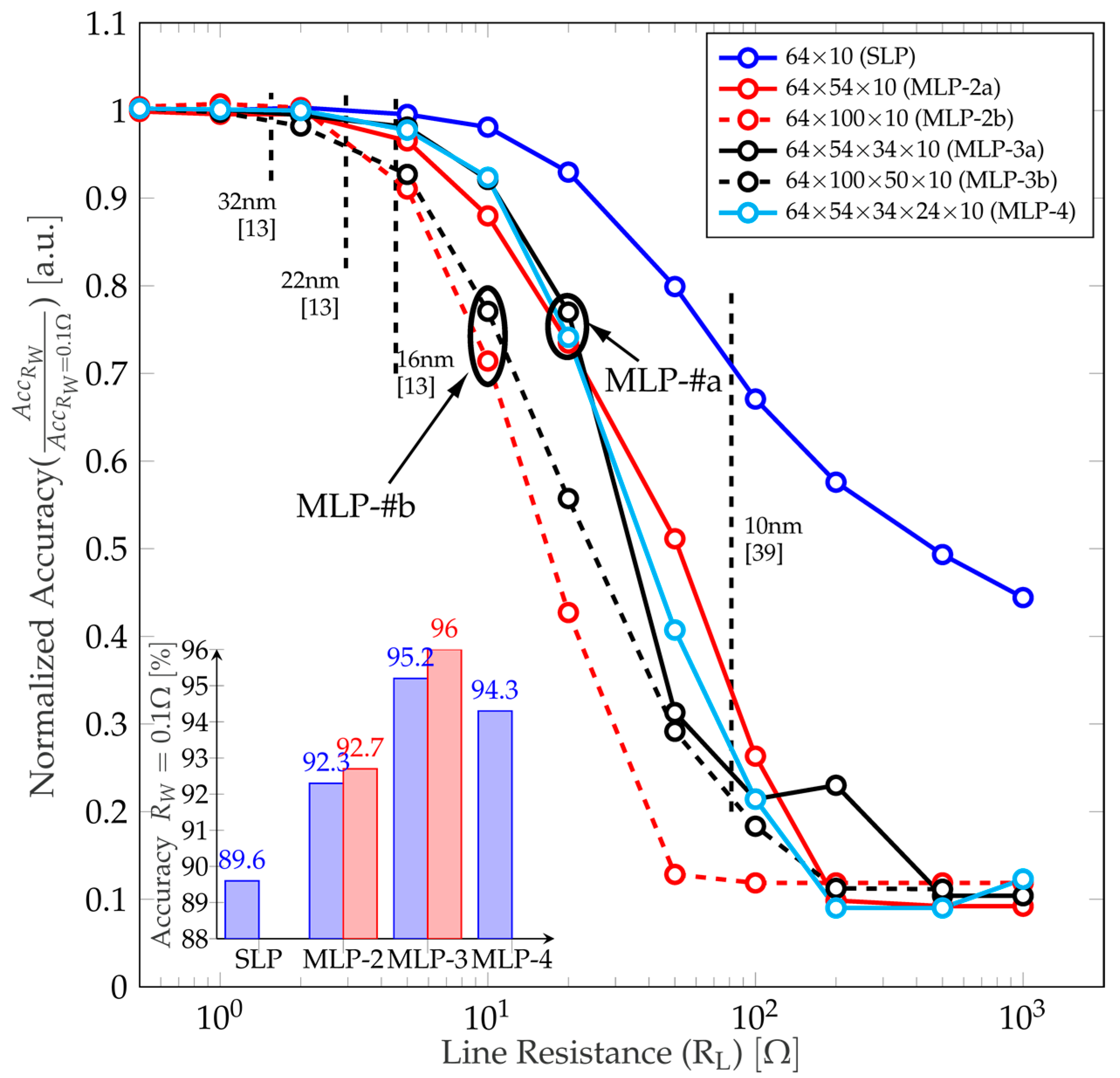
Figure 1. (a) Sketch of the MCA structure. Red and blue arrows show currents from the top (word lines—WL) to the bottom lines (bit lines—BL). Different resistance states are represented (high (HRS) to low (LRS) resistance states). The dashed blue line depicts the sneak path problem. The parasitic R L is indicated for WLi and BLi. Two MCAs are depicted, representing two layers of synapses. (b) Sketch of a DNN with two hidden layers.
Jlpea 11 00009 g001
Figure 2. (a) Hysteron model with logistic ridge functions Γ+ (Equation (3)) and Γ (Equation (4)). Ω is the space of feasible states S. The red thick faded line superimposed to the hysteron model indicates the trajectory of the state variable λ inside Ω from an initial S1 to a final S2 state. The inset in the right shows the equivalent circuit model for the current equation (Equation (1)) including the series resistance. The diodes are driven by the memory state of the device and one diode is activated at a time. Typical I-V characteristic for a memdiode obtained via simulation of the proposed model are superimposed. Current evolution is indicated by the blue arrows. (b) I-V characteristics of the memdiode showing the exponential (HRS) to lineal (LRS) transition by varying λ. The red shaded region indicates the possible voltages applied to the device as the read margin reduces. IHRS and ILRS currents are pinpointed at nominal Vread with the grey and white circle markers, respectively. Overestimation of IHRS may occur when considering a linear model for the HRS regime and lower effective Vread voltages as indicated by the cyan, blue and black ball markers. (c) Experimental I-V loops of different materials reported in the literature fitted with the QMM model: Al2O3 [47] and TaOX [46].
Jlpea 11 00009 g002
Figure 3. (a) Samples of the MNIST database considered in this article. In all cases images are represented in 28 × 28 px. Pixel brightness (or intensity) is codified in 256 levels ranging from 0 (fully OFF, black) to 1 (fully ON, white). (b) Readability loss as the resolution decreases from 28 × 28 px (case I) to 8 × 8 (case VII). (c) Flowchart diagram for the simulation procedure. Starting with the image size specification, RL, Vread, and connection scheme, the routine creates the dataset, trains the MLP, translates it into an MCA, performs the simulations and processes the results. (d) Flowchart diagram of the calibration method to minimize the impact of RL. It is included in block 5 from (c).
Jlpea 11 00009 g003
Figure 4. (a) Simplified equivalent circuit schematic for a partitioned MCA-based MLP. Each MCA in the 1st synaptic layer is subdivided into N identically sized partitions to minimize the parasitic voltage drops. Partial output current vectors are indicated in the output of each partition. (b) Equivalent circuit schematic for an MCA based SLP. Red and blue arrows exemplify the electron flow through the memdiodes connecting the top (word lines—WL) and bottom lines (bit lines—BL). The dashed blue line depicts the so-called sneakpath problem. (c) Individual RRAM cell with the associated RL resistors.
Jlpea 11 00009 g004
Figure 5. Inference accuracy vs. RL, normalized against the inference accuracy obtained for RL→0 Ω. Two different sets of MLP (#a and #b, see Table 1 for details) are considered as well as a SLP for comparison purposes. The inset in the lower left shows the inference accuracy at RL→0 Ω for the different cases considered. Note that the RL dependency of the inference accuracy is determined by the size of the largest MLP layer, and it presents a very shallow dependence on the number of hidden layers. In fact, the increase in the number of hidden layers allows boosting the inference accuracy as RL decreases without compromising the MLP sensitivity to RL variations.
Jlpea 11 00009 g005
Figure 6. Inference accuracy plotted against the line resistance (RL) for four different scenarios: SLPs considering (a) 8 × 8 px. images (the SLP structure is 64 × 10) and (b) 14 × 14 px. (196 × 10) and MLP considering (c) 8 × 8 px. images (64 × 54 × 10) and (d) 14 × 14 px. images (196 × 20 × 10). The ideal results considering software implementation of the same networks is added in each subfigure by a red dash-dotted line. For (a,b) both the calibration and partitioned implementations are superimposed for comparison. Instead for (c,d) only the partitioned scenario is shown as no relevant improvement was found by the calibration procedure. The inset in (a) shows the optimal calibration factor as function of RL.
Jlpea 11 00009 g006
Table 1. Structures of the MLPs considered in the simulations of this section. In all cases the MNIST images resized to 8 × 8 px are considered as the input pattern.
Hidden LayersCodeNetwork StructureNumber of Memristive Sys.Accuracy at RL→0 ΩAccuracy (Soft. Case)
0SLP64 × 101280 sys.89.6%91.14%
1MLP-2a64 × 54 × 107992 sys.92.3%95.95%
MLP-2b64 × 100 × 1014,800 sys.92.7%96.89%
2MLP-3a64 × 54 × 34 × 1011,263 sys.95.2%96.30%
MLP-3b64 × 100 × 50 × 1023,800 sys.96%96.92%
3MLP-464 × 54 × 34 × 24 × 1012,696 sys.94.3%95.81%
Publisher’s Note: MDPI stays neutral with regard to jurisdictional claims in published maps and institutional affiliations.

