1. Introduction
Source-follower (SF) analog filters are a well-established and popular topic in analog filter design [
1,
2,
3,
4,
5]. They exploit the intrinsic features of source follower stages, such as large bandwidths at low noise powers, low harmonic distortion, and limited power consumption. These features make SF filters very attractive for new-generation telecommunication transceivers [
6] and front-end analog sensors [
7] where analog filter bandwidths have been raised up to 50/100 MHz to fit the increasing communication rate.
These innovative applications force analog filters to comply with stringent noise power spectral density (PSD) requirements because the noise is spread over a wider bandwidth, imposing lower in-band noise PSD at constant integrated noise power [
8]. Nonetheless, lower in-band noise PSD should be accompanied by an (almost) rail-to-rail output swing to avoid dynamic range drops for the following A-to-D converter.
Dedicated analog solutions based on open-loop g
m-C filters [
9] have intrinsic low-noise and low-power performances that partially fit the telecommunications requirements. On the other hand, g
m-C filters are not able to preserve linearity, unless to increase overdrive voltage that is often not an option in nanometer-range technologies where voltage headroom (V
DD − V
TH; supply and threshold, respectively) is significantly smaller. Nonetheless, increasing overdrive leads to increasing power at constant transconductance (g
m) and, moreover, intrinsically limits the available output voltage swing (and thus dynamic range, which is further reduced by scaled-down V
DD, not higher than 1 V for standard-process (SP) MOS transistors (MOST) in CMOS 65 nm and below).
For these reasons, several studies in the literature [
10,
11,
12,
13,
14] exploit closed-loop active-RC solutions that meet linearity specifications, and easily manage rail-to-rail output swings, whereas they require an intrinsic power budget to be allocated to the larger unity gain frequency amplifiers. In this scenario, some studies have explored alternative circuital options, taking advantage of the low noise, low power, and large linearity performance of SF filters.
1.1. Source-Follower Filter State-of-the-Art vs. CMOS Technology
State-of-the-art SF filters adopt scarcely scaled-down technological nodes (0.13 µm [
1] and 0.18 µm [
2,
3,
4,
5] CMOS at 1.2 V and 1.8 V supply voltage, respectively, for SP MOST). One of the main motivations is the intrinsic operating DC voltage difference between input/output (gate/source) nodes for biasing. Moreover, both 0.13 µm and 0.18 µm CMOS operate with a safe operating point voltage headroom (V
DD-V
TH = 1.3 V and 0.9 V, respectively), enabling a moderate inversion region for SF input MOSTs (for instance, M1 in
Figure 1). This increases the characteristic transconductance (g
m), minimizes in-band noise power spectral density (PSD), and improves linearity performance when input tone frequency approaches filter pole frequency. In other words, SF filters well adapt to 0.13 µm [
1] and 0.18 µm [
2,
3,
4,
5] CMOS nominal characteristics, resulting in very advanced and efficient circuital solutions.
In [
2] he single N-channel MOST SF has been improved by including a second gain stage (based on a p-channel MOST) in the direct path of the closed-loop scheme that allows synthesis of a specific complex pole pair and to separately optimize the two MOSTs (the input stage MOST for noise and linearity; the second stage MOST for loop-gain enhancement), increasing the circuit efficiency. If the additional gain stage is a P-channel device, and the input stage MOST is an N-channel type, mismatch between two different MOST carriers’ mobility could be an issue for the closed-loop transfer function, where both MOSTs operate with their own transconductances. Moreover, an additional PMOS gain stage requires additional current consumption to be allocated directly to the stage (increasing power) or to be subtracted from the input stage (increasing noise).
In order to overcome these issues, M. De Matteis et al. [
3] proposes (by Spice simulations) to adopt the flipped version of the SF circuit, where two cascode MOSTs concentrate the gain in the same stack, have the same channel carrier typology, and maintain the separation between noise/linearity (input MOST) and loop gain (the bottom MOST in the cascode). Unfortunately, this solution, even presenting an efficient design results (large in-band linearity with >20 dBm input IP3 and 5.8 nV/√Hz in-band noise PSD), scarcely fits with the reduction in both V
DD-V
TH (0.5 V in 28 nm CMOS against 1.3 V in 0.18 µm CMOS) voltage headroom for biasing and MOST intrinsic gain.
Xu Yang, et al. [
4,
5] present a similar biquadratic (biquad) cell concept in CMOS 0.18 μm technology nodes. Both devices achieve large in-band IIP3 and, importantly, operate with 1.35 V and 1.3 V supply voltages at 0.55 V nominal threshold voltages for SP MOST in CMOS 0.18 μm, approaching, without targeting, nanometer-range technology scenarios.
1.2. CMOS 28 nm Flipped-Source-Follower Filter
The filter presented here [
15] advances the state of the art by:
The filter is composed of the cascade of two biquads, synthesizing a 100 MHz pole frequency response and consuming 968 µW power from a single 1 V supply voltage. Measured input IP3 is 12.5 dBm and 2.5 dBm for 10 and 11 MHz and 50 and 51 MHz input tones, respectively. The final achieved figure-of-merit outperforms the state-of-the-art filters with 160 dBJ-1@10 and 11 MHz and 160.7 dBJ-1@50 and 51 MHz.
This paper is organized as follows.
Section 2 presents the transistor-level scheme of the filter and most relevant design aspects in terms of operating point, closed-loop, and loop-gain transfer function, noise, and linearity.
Section 3 shows the experimental validation of the filter prototype carried out by both time and frequency domain electrical characterizations. Finally, at the end of the paper, conclusions will be drawn.
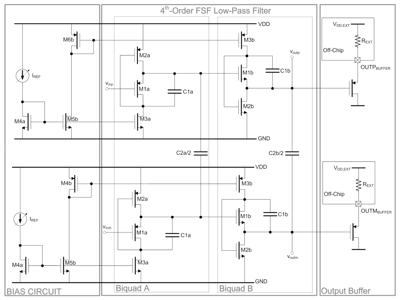
2. Flipped-Source-Follower Filter Transistor-Level Design
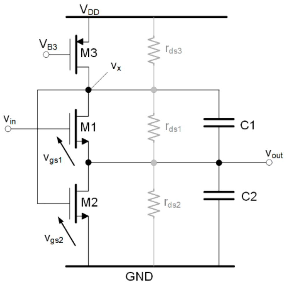
The transistor-level scheme of the proposed biquadratic cell based on FSF analog stage is shown in
Figure 1. The FSF filter is composed of an M1-M2 MOST biased by a current source (M3). C
1-C
2 capacitances with g
m1-g
m2 (M1-M2 transconductances) synthesize a specific pair of complex conjugated poles. r
ds1, r
ds2 and r
ds3 are the output resistances of M1, M2 and M3 MOSTs, respectively.
The M1 gate-source voltage swing is strongly reduced by the M1-M2 loop-gain and all the nodes of the circuit (whose electrical voltages are vout and vx) have lower impedance to the ground compared to what was happening without the action of the loop-gain (low frequency output impedance to ground is approximately equal to 1/(gm1·gm2·rds3) and M1 drain node impedance to ground is approximately equal to 1/gm2).
This implies that both M1 and M2 have very limited gate-source voltage (V
GS) swings. As a result, the biquad cell presented in
Figure 1 synthesizes a specific complex pole pair, while ideally zeroing the gate-source voltage swing of all MOSTs, thus minimizing harmonic distortion (among other aspects directly proportional to the voltage swing at the MOST gate node). Moreover, at the first order, because M1 drain and source nodes have very small equivalent impedance to ground, any M2 noise current will flow by ground with negligible noise voltage swing.
2.1. Operating Point and Output Signal Swing
The input transistor (M1) operates with a finite DC voltage between gate and source nodes for biasing. A strong inversion region would limit the output swing, reducing the dynamic range (DR) for a given noise power.
On the other hand, a sub-threshold region leads to higher harmonic distortion power when the input tone frequency approaches the closed-loop pole frequency (where the filter has very small loop-gain and linearity is no longer preserved by the loop gain). Therefore, a larger VOV would mitigate this increasing distortion at higher frequencies.
For these reasons, this design adopts a trade-off approach between DR maximization and harmonic distortion reduction, by setting the biasing overdrive voltage (VOV = VGS-VTH) at 75 mV for both M1-M2 (i.e., the transition voltage point between weak and moderate inversion regions). This choice preserves DR while avoiding the deep sub-threshold region, where high-frequency distortion should dramatically increase.
Assuming that all MOSTs have the same V
TH and V
OV, then the input common-mode voltage (V
in,CM) of the biquad n-channel M1 MOST input stage and the input voltage swing (V
in,SW) are limited by the following relationship:
Hence, V
in,CM + V
in,SW ranges from 0.65 V to 1 V (VDD), with V
TH ≈ 0.5 V and V
OV = 0.075 V. This design adopts V
in,CM = 0.825 V, to maximize the filter input signal swing (V
in,SW = 0.175 V
0-PEAK) that perfectly matches with the output swing limitations as follows. The M1 source common mode voltage (V
out,CM) is limited by Equation (2):
Thus, Vout,CM = Vin,CM − (VTH + VOV) = 0.25 V agrees with a ±0.175 V0-PEAK input/output swing.
The design approach operates both M1-M2 without considering body effect (which is non-null in M1). This leads to a slight mismatch between two transconductances, resulting in limited quality factor and pole frequency deviation that can be easily adjusted by recalculating C1-C2 values.
2.2. Biquad Closed-Loop Transfer Function
The biquad transfer function (assuming infinite MOST output resistances) is given by Equation (3):
It features 0 dB DC gain. Pole frequencies (ω
0) and quality factors (
Q) are given by:
2.3. Biquad Loop Gain
The proposed FSF filter uses C
1-C
2 capacitances for synthesizing complex conjugated poles. This changes the loop gain, compared with generic FSF buffers, in terms of lower unity gain frequency (which is now, in first approximation, equal to the filter closed-loop pole frequency). Equation (5) reports loop-gain transfer function including, in addition to g
m1-g
m2 and C
1-C
2 pairs, all MOST output drain-source resistances:
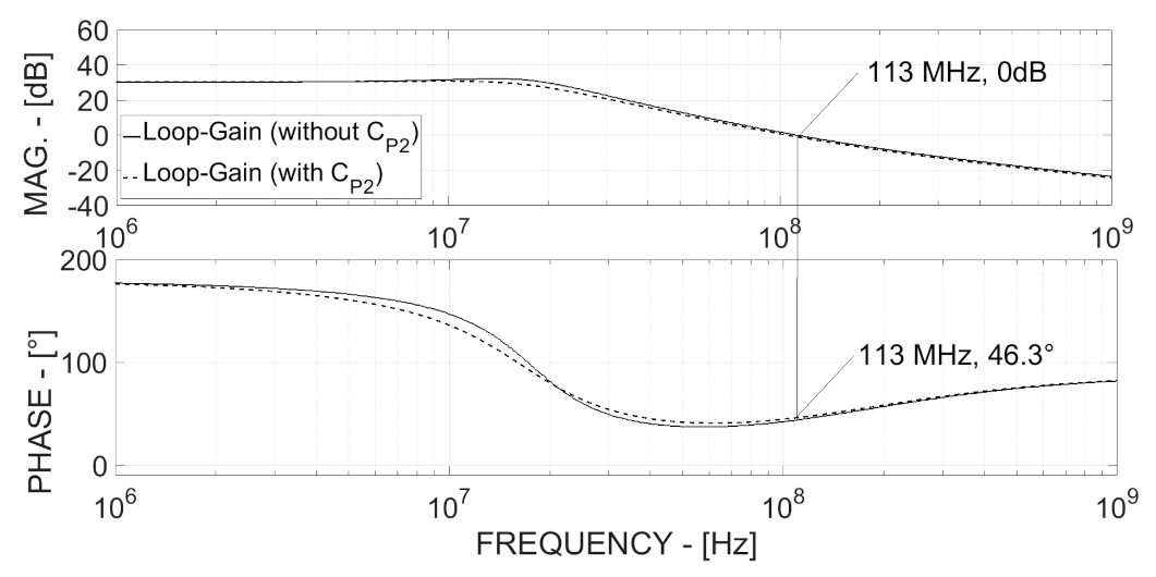
The loop-gain magnitude and phase frequency response are plotted in
Figure 2, with and without the effect of the M2 gate-source parasitic capacitance (C
P2) which does not significantly modify the phase margin at the unity gain frequency and whose impact is negligible comparing with C
1-C
2. FSF has lower loop-gain at higher frequency while approaching the pole frequency.
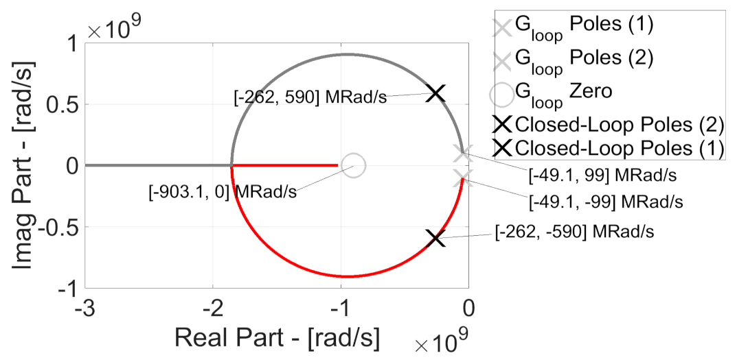
Figure 3 shows the Gauss plane root locus of the FSF biquad cell, where the loop-gain poles and zero with closed-loop poles are plotted, and as expected, the locus is attracted by the zero (whose frequency is 2·π·g
m1/C
1≈900 MRad/s) and moved away from the poles ((−49.1 ± j·99) MRad/s which have an equivalent quality factor (Q
Loop) equal to 1.12).
The root locus (starting in the negative real part Gauss plane region) moves towards the left half Gauss plane, without any eventual stability issue.
Table 1 lists the values of the root locus main singularities, and
Table 2 reports the design parameters of each cell.
The filter is composed of the cascade of two biquads, and this analysis is referred to the higher quality factor (Q = 1.3066).
2.4. Biquad Linearity Performances
Inter-modulation (IM) distortions in FSF biquads are substantially set by M1 and M2. M3 operates as a current source and it does not introduce a relevant distortion contribution in its first approximation. The M1 IM distortion power ratio of the two components at ω
1 ± ω
2 to the fundamental, called IM
3,M1 (IM
3,M2), is measured at the output of the FSF biquad and it is in first approximation depending on two key design parameters: the amount of M1 (M2) gate-source voltage swing (v
gs1 and v
gs2) vs. the overdrive voltage and the loop gain [
15,
16].
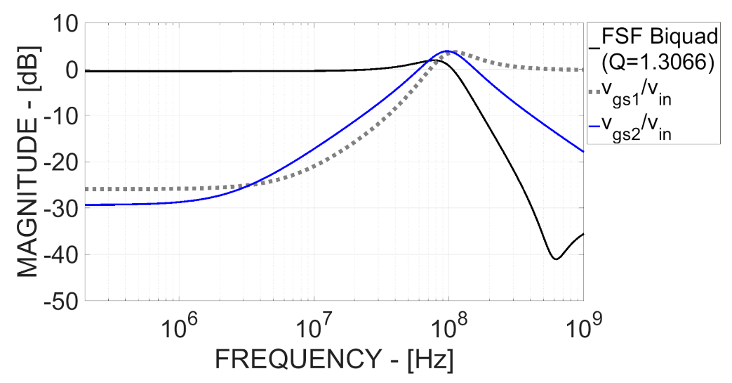
Figure 4 shows v
gs1/v
in and v
gs2/v
in frequency responses extracted by the following transfer functions, referring to the scheme in
Figure 1:
Notice that:
vgs1/vin magnitude frequency response has a −27 dB dc gain, two zeros, and two poles, inducing high-frequency 0 dB gain;
vgs2/vin is −30 dB at low frequency, has one zero and two poles, and this implies −20 dB/decade high frequency drop.
It follows that the FSF biquad has low distortion power at low frequency (where the signal is lower, and the loop-gain is higher) and IM distortion increases at high frequency while approaching the closed-loop pole frequency.
Assuming to operate with both M1 and M2 MOSTs at V
OV1 = V
OV2 = 75 mV, IM
3,M1 and IM
3,M2 are given by:
where
Gloop is the loop-gain of the biquad, whose transfer function is reported in Equation (5). As a result,
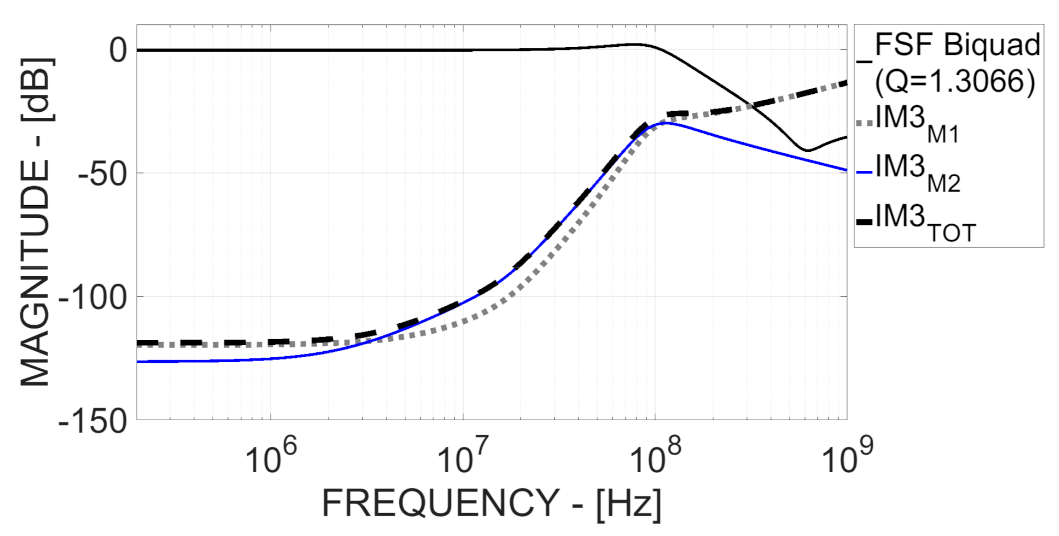
Figure 5 shows IM
3,M1 and IM
3,M2 vs. frequency (with v
in1 = v
in2 = 10 mV
0-PEAK amplitude, i.e., −30 dBm power-per-tone). The total IM
3 resulting from both M1-M2 distortion contributions is also plotted. IM
3 is dominated by the M1 MOST up to approximately 10 MHz, whereas from 10 MHz up to 100 MHz, the distortion contribution due to M2 MOST becomes more important.
Figure 4 and
Figure 5 curves were obtained by simulating a MATLAB small-signal model of the biquad B, whose main design parameters are listed in
Table 2. IM
3TOT is −118 dB at low frequency, and it rises to −28 dB at 100 MHz; therefore, the resulting simulated input IP3 for the FSF biquad will range from 29 dBm at low frequency down to −2 dBm at 100 MHz, which is in line with the expected measurement results for single cell linearity.
2.5. Biquad Noise Performances
There are three noise sources that contribute to the final input referred noise (IRN) power spectral density:
Here,
,
and
are M1, M2 and M3 MOST thermal noise voltage sources and they are in first approximation given by the following equation:
For these MOSTs operating at the transition point between weak and moderate inversion regions, the characteristic transconductance can be in first approximation equal to I
1/(n
N·V
Thermal) for n-channel MOST (or I
1/(n
P·V
Thermal) for p-channel MOST devices). I
1 is the M1-M2-M3 common DC current, V
thermal is 25 mV at room temperature, and n
N-n
P are the sub-threshold slope factors [
17], which in first approximation are dependent on the MOST depletion layer and oxide capacitances).
Hence, Equation (10) can be simplified as follows:
Assuming nN ≈ nP, the target of 7 nV/√Hz noise PSD for a fourth-order low pass filter (equivalent to 5 nV/√Hz noise PSD per-biquad), is achieved with gm1 = 1.8 mA/V at 242 µA bias current for each single branch cell.
3. Experimental Measurements Results
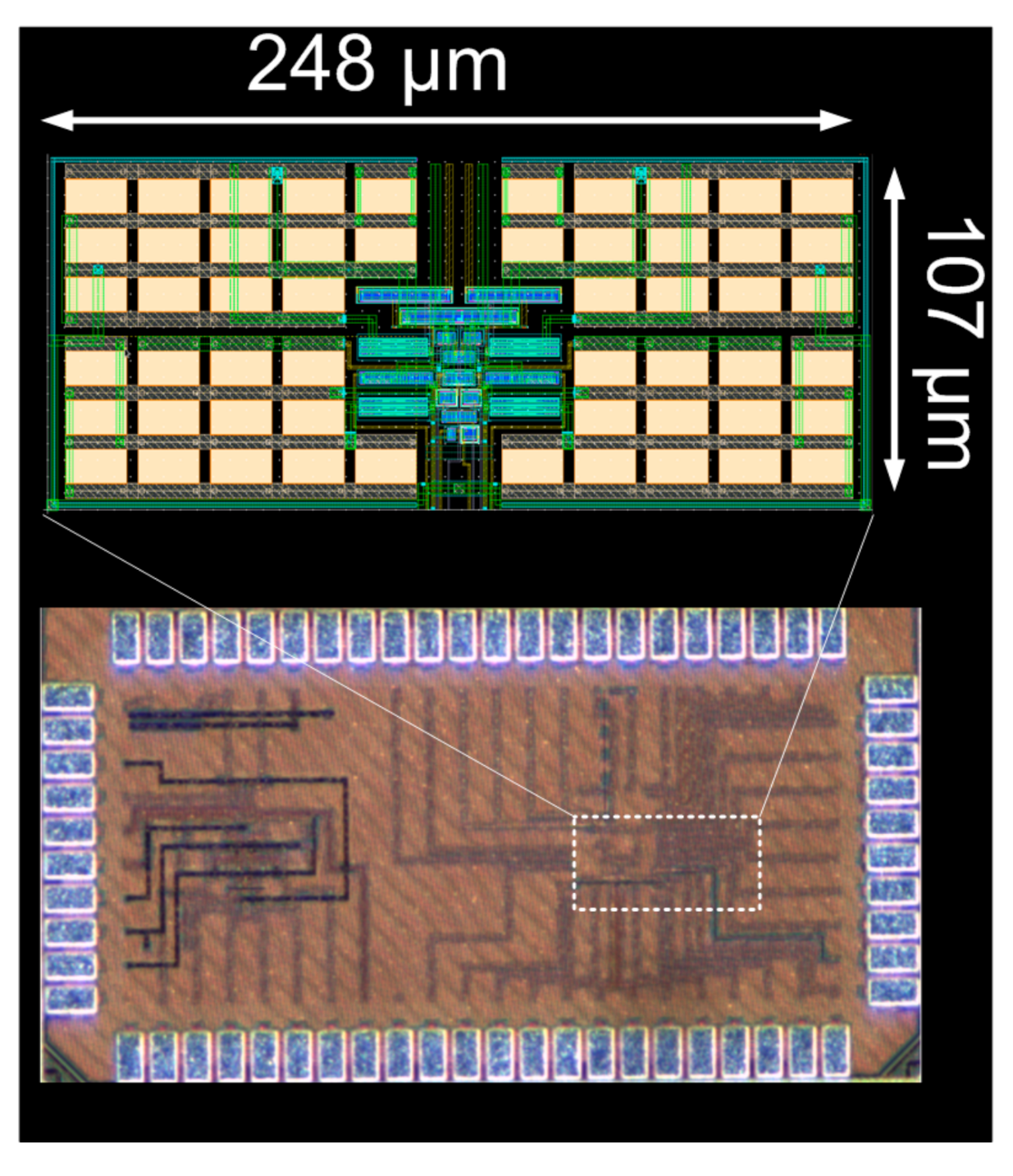
The transistor-level pseudo-differential scheme of the proposed filter is shown in
Figure 6. The device has been integrated in 28 nm CMOS technology and fully characterized in terms of operating point, frequency, and time domain performances. The chip and layout photo are shown in
Figure 7. The whole FSF filter occupies 0.026 mm
2.
The fourth-order filter cascades two biquad cells (Biquad A at Q = 0.5412 and Biquad B at Q = 1.3066).
The lower quality factor cell is placed at the beginning of the cascade, performing some filtering of the in-band and out-of-band power with the main aim of improving linearity performance (at the cost of a slight noise increase). Specific output buffers based on a PMOS source follower have been used to drive the output load (mainly capacitive and in the order of some pF).
The bias reference current is used to align the filter frequency response in front of CMOS process technological variations.
Total power consumption (excluding both bias circuit and output buffers) is 0.968 mW. The measured power consumption per biquad is 0.4356 mW (0.2178 mW per branch) for biquad A and 0.532.4 mW for biquad B (0.266.2 mW per branch).
Biquad B uses a slightly higher current because it should synthesize the higher quality factor, and intrinsically require more bandwidth.
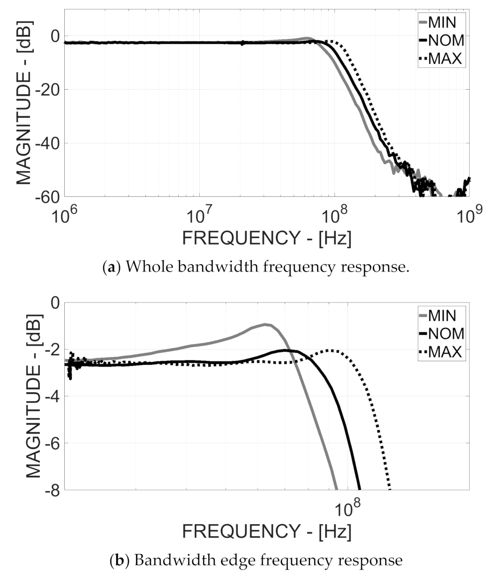
3.1. Frequency Response
Figure 8 shows whole pass-band (and pass-band right edge) filter frequency responses in nominal conditions (nominal I
REF of 10 µA) and with maximum and minimum currents (where I
REF is 12 µA and 8 µA, respectively). The filter DC gain is −2.5 dB. This drop is mainly due to the output buffer that has been biased to maximize bandwidth at the cost of a small gain reduction.
The measured −3 dB frequency was 100 MHz at nominal IREF, whereas it ranged from 85 MHz to 120 MHz for max. and min. IREF. The maximum in-band ripple was +1.5 dB for max IREF frequency response, and it was lower than 0.5 dB for the minimum and nominal IREF.
3.2. Linearity Performance
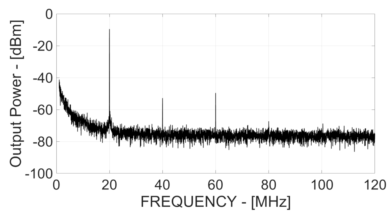
The filter linearity has been characterized by single and double tone tests. The output spectrum of a 0.33 V
0-PEAK output signal at 20 MHz input frequency is shown in
Figure 9. The third-order harmonic distortion is dominant, and it is equal to −49.5 dB, resulting in a Total-Harmonic-Distortion (THD) of −40 dBc.
The total output noise power is 98 µV
RMS. In this way, the final FSF filter DR for −40 dBc@THD is 67.6 dB, which is, in some cases, better than the state-of-the-art analog filters in the literature, as illustrated in
Table 3 [
2,
4,
5,
10,
11,
12,
13,
14,
17,
18,
19,
20].
Importantly, this FSF filter maintains the SNR performance compared with state-of-the-art analog devices, even when using the most scaled-down technology.
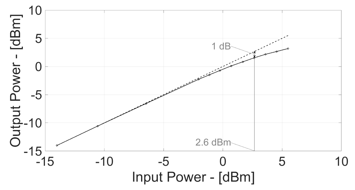
The 1 dB compression point (1dB-CP) of 2.6 dBm (0.426 V
0-PEAK output voltage) has been measured, and the corresponding input/output characteristics are shown in
Figure 10.
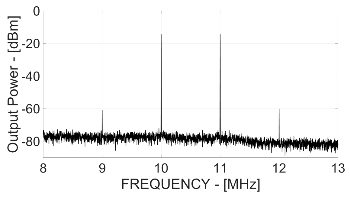
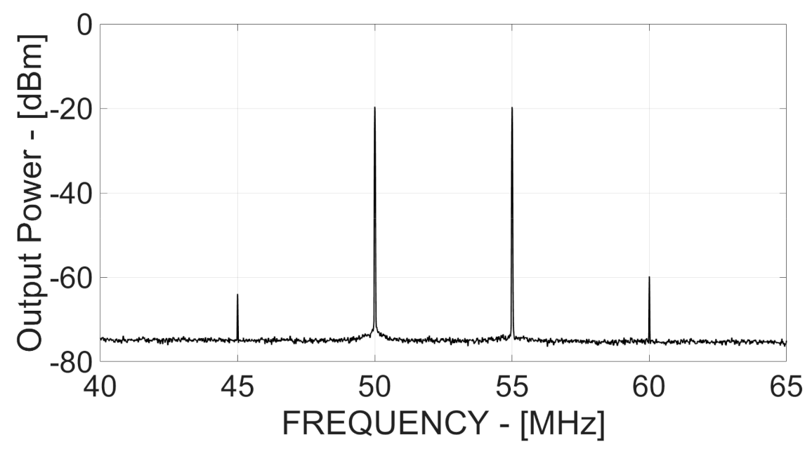
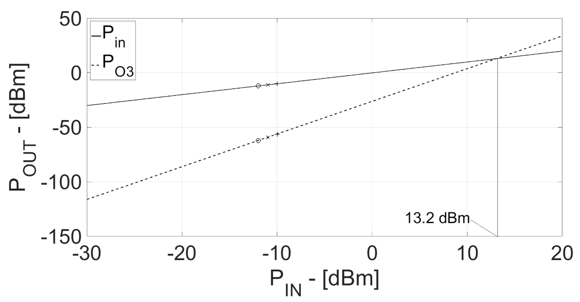
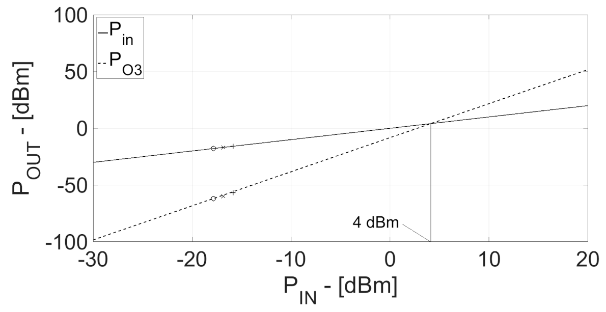
Figure 11 and
Figure 12 show the two-tone output spectra for 10 and 11 MHz and 50 and 55 MHz input tones frequency.
The third-order intermodulation product is −46 dB and −40 dB, respectively (with a two output iso-power tones of −14 dBm and −20 dBm).
This gives an input IP3 of 13.2 dBm and 4 dBm at 10 and 11 MHz and 50 and 55 MHz input tones frequency, respectively, as shown in
Figure 13 and
Figure 14.
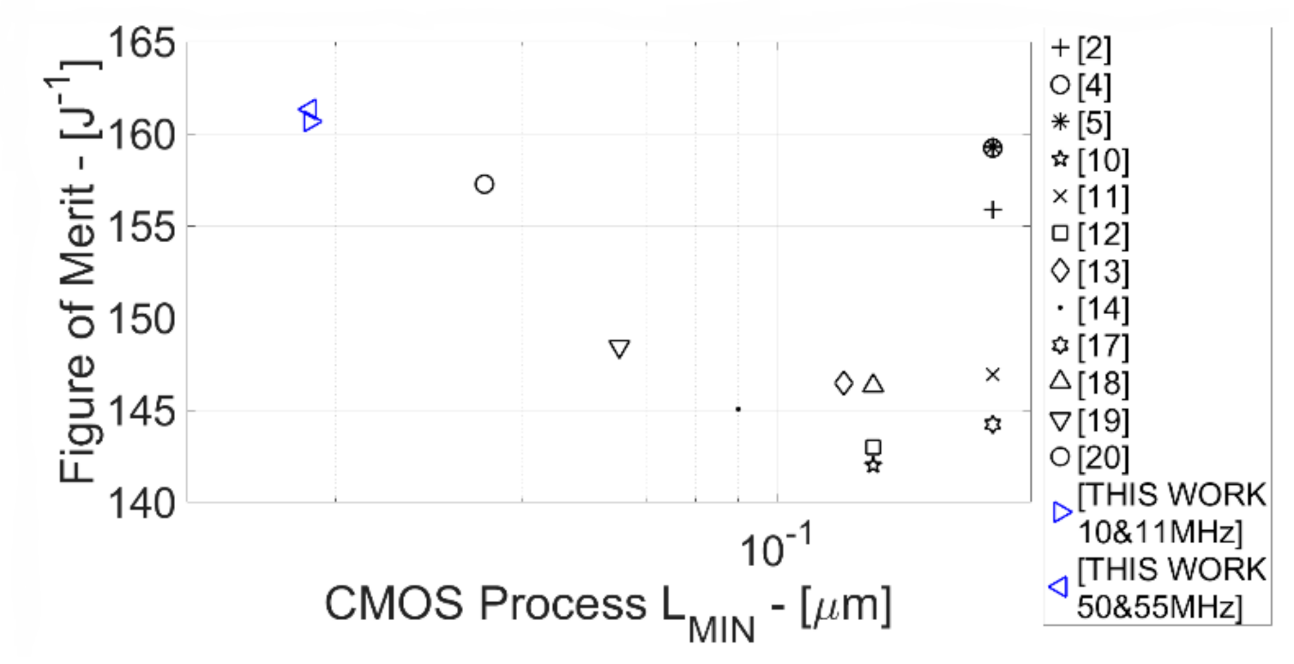
Finally, this filter has been compared with the state-of-the-art filters by adopting the following figure-of-merit (FoM [
2]):
where PW is the total power consumption, f
−3dB is the cut-off frequency,
N is the number of poles, and
IMFDR3 is the spurious-free IM3. Such FoM takes into account the distance of the inter-modulation products from the pole frequencies by including the ratio between the lower frequency third-order inter-modulation tone (f
IM3,LOW) and the pole frequency (f
POLES), as discussed in [
2].
The filter achieves the significant 160 and 161 dBJ
−1 FoM (for 10 and 11 MHz and 50 and 55 MHz, respectively, as shown in
Figure 15), outperforming analog filter implementations in scaled nodes (<130 nm), enabling 28 nm CMOS analog filters for future telecommunications wireless transceivers.
4. Conclusions
In this paper, both complete design and electrical/experimental characterization of a fourth-order flipped-source-follower filter have been presented. The device synthesizes a fourth-order low-pass Butterworth transfer function at 100 MHz −3 dB frequency using a single cascode stack, optimizing a noise/power trade-off and improving matching comparing with source-follower state-of-the-art analog filters. Moreover, this paper proposes the most scaled-down CMOS implementation of FSF filters operating with the lower supply voltage (1 V). The device achieved one of the better FoM (and the most scaled CMOS process) compared with the state-of-the-art filters (160 dBJ−1).
Author Contributions
Conceptualization and Methodology, M.D.M.; Validation, M.D.M., E.A.V. and F.F.; data curation, M.D.M.; Validation, M.D.M., E.A.V.; writing—original draft preparation, writing—review and editing, M.D.M., E.A.V., F.F. and A.B.; supervision, M.D.M.; project administration, funding acquisition, A.B. All authors have read and agreed to the published version of the manuscript.
Funding
This research was funded by AnyThing project (within Research Projects of National Interest (PRIN 2015), grant number 2015ABZ44K.
Conflicts of Interest
The authors declare no conflict of interest.
References
- Baschirotto, A.; D’Amico, S.; De Matteis, M. Advances on analog filters for telecommunications. In Proceedings of the Advanced Signal Processing, Circuits, and System Design Techniques for Communications—2006 IEEE International Symposium on Circuits and Systems, ISCAS 2006, Kos, Greece, 21–24 May 2006; pp. 131–138. [Google Scholar]
- De Matteis, M.; Pezzotta, A.; D’Amico, S.; Baschirotto, A. A 33 MHz 70 dB-SNR super-source-follower-based low-pass analog filter. IEEE J. Solid-State Circuits 2015, 50, 1516–1524. [Google Scholar] [CrossRef]
- De Matteis, M.; Baschirotto, A. A Biquadratic Cell based on the Flipped-Source-Follower Circuit. IEEE Trans. Circuits Syst. II Express Briefs 2017, 64, 867–871. [Google Scholar] [CrossRef]
- Xu, Y.; Leuenberger, S.; Venkatachala, P.K.; Moon, U.-K. A 0.6 mW 31 MHz 4th-order low-pass filter with+ 29 dBm IIP3 using self-coupled source follower based biquads in 0.18 µm CMOS. In Proceedings of the 2016 IEEE Symposium on VLSI Circuits, Honolulu, HI, USA, 15–17 June 2016; pp. 1–2. [Google Scholar]
- Xu, Y.; Muhlestein, J.; Moon, U.-K. A 0.65 mW 20 MHz 5th-order low-pass filter with+ 28.8 dBm IIP3 using source follower coupling. In Proceedings of the 2017 IEEE Custom Integrated Circuits Conference (CICC), Austin, TX, USA, 30 April–3 May 2017; pp. 1–4. [Google Scholar]
- Hong, S.; Brand, J.; Choi, J.; Jain, M.; Mehlman, J.; Katti, S.; Levis, P. Applications of self-interference cancellation in 5G and beyond. IEEE Commun. Mag. 2014, 52, 114–121. [Google Scholar] [CrossRef]
- De Matteis, M.; Resta, F.; Richter, R.; Kroha, H.; Fras, M.; Zhao, Y.; Abovyan, S.; Baschirotto, A. An Eight-Channels 0.13µm-CMOS Front End for ATLAS Muon-Drift-Tubes Detectors. IEEE Sens. J. 2017, 17, 3406–3415. [Google Scholar] [CrossRef]
- De Matteis, M.; D’Amico, S.; Baschirotto, A. Power-minimization design procedure for Rauch biquadratic cells. In Proceedings of the 2006 Ph.D. Research in Microelectronics and Electronics, Otranto, Italy, 12–15 June 2006; pp. 141–144. [Google Scholar]
- Saari, V.; Kaltiokallio, M.; Lindfors, S.; Ryynänen, J.; Halonen, K. A 240-MHz low-pass filter with variable gain in 65-nm CMOS for a UWB radio receiver. IEEE Trans. Circuits Syst. I Regul. Papers 2009, 56, 1488–1499. [Google Scholar] [CrossRef]
- Amir-Aslanzadeh, H.; Pankratz, E.J.; Sanchez-Sinencio, E. A 1-V +31 dBm IIP3, reconfigurable, continuously tunable, power-adjustable active-RC LPF. IEEE J. Solid-State Circuits 2009, 44, 495–508. [Google Scholar] [CrossRef]
- Thyagarajan, S.V.; Pavan, S.; Sankar, P. Active-RC filters using the Gm-assisted OTA-RC technique. IEEE J. Solid-State Circuits 2011, 46, 1522–1533. [Google Scholar] [CrossRef]
- Kousai, S.; Hamada, M.; Ito, R.; Itakura, T. A 19.7 MHz, fifth-order active-RC Chebyshev LPF for draft IEEE802.11n with automatic quality-factor tuning scheme. IEEE J. Solid-State Circuits 2007, 42, 2326–2337. [Google Scholar] [CrossRef]
- Vasilopoulos, A.; Vitzilaios, G.; Theodoratos, G.; Papananos, Y. A low-power wideband reconfigurable integrated active-RC filter with 73 dB SFDR. IEEE J. Solid-State Circuits 2006, 41, 1997–2008. [Google Scholar] [CrossRef]
- Oskooei, S.; Masoumi, N.; Kamarei, M.; Sjoland, H. A CMOS 4.35-mW +22-dBm IIP3 continuously tunable channel select filter for WLAN/WiMAX receivers. IEEE J. Solid-State Circuits 2011, 46, 1382–1391. [Google Scholar] [CrossRef]
- Fary, F.; De Matteis, M.; Vergine, T.; Baschirotto, A. A 28 nm-CMOS 100 MHz 1 mW 12 dBm-IIP3 4th-Order Flipped-Source-Follower Analog Filter. In Proceedings of the ESSCIRC 2018-IEEE 44th European Solid State Circuits Conference, Dresden, Germany, 3–6 September 2018; pp. 298–301. [Google Scholar]
- Sansen, W. Distortion in elementary transistor circuits. IEEE Trans. Circuits Syst. II Analog Digit. Signal Process. 1999, 46, 315–325. [Google Scholar] [CrossRef]
- Ye, L.; Shi, C.; Liao, H.; Huang, R.; Wang, Y. Highly power-efficient active-RC filters with wide bandwidth-range using low-gain push-pull opamps. IEEE Trans. Circuits Syst. I Regul. Pap. 2012, 60, 95–107. [Google Scholar] [CrossRef]
- Mobarak, M.; Onabajo, M.; Silva-Martinez, J.; Sanchez-Sinencio, E. Attenuation-predistortion linearization of CMOS OTA with digital correction of process variations in OTA-C filter Applications. IEEE J. Solid-State Circuits 2010, 45, 351–367. [Google Scholar] [CrossRef]
- Lim, J.; Kim, J. A 20-kHz~16-MHz Programmable-Bandwidth 4th Order Active Filter Using Gain-Boosted Opamp With Negative Resistance in 65-nm CMOS. IEEE Trans. Circuits Syst. II Express Briefs 2018, 66, 182–186. [Google Scholar] [CrossRef]
- Panigrahi, A.; Parhi, A. 1.2 V, 12.5 MHz fourth-order low-pass filter with 83 dB stopband attenuation using low output impedance source follower in 45 nm CMOS. IET Circuits Devices Syst. 2018, 12, 382–389. [Google Scholar] [CrossRef]
| Publisher’s Note: MDPI stays neutral with regard to jurisdictional claims in published maps and institutional affiliations. |
© 2021 by the authors. Licensee MDPI, Basel, Switzerland. This article is an open access article distributed under the terms and conditions of the Creative Commons Attribution (CC BY) license (https://creativecommons.org/licenses/by/4.0/).


