
Internet of Things: A Review on Theory Based Impedance Matching Techniques for Energy Efficient RF Systems

 , ,
, ,  ,
,  ,
,
Abstract
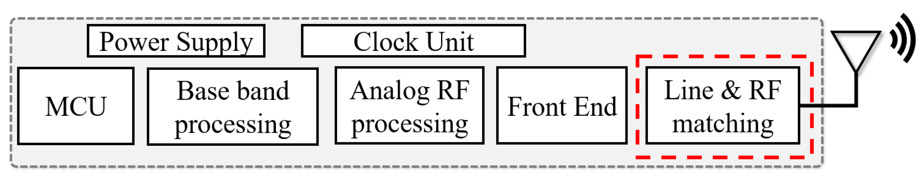
:1. Introduction
2. Formal Expressions of the Power Gain in Typical RF Systems
2.1. ABCD-Parameters Approach
2.2. Transducer Gain
2.3. Transmission Lines Approach
2.4. Power Waves
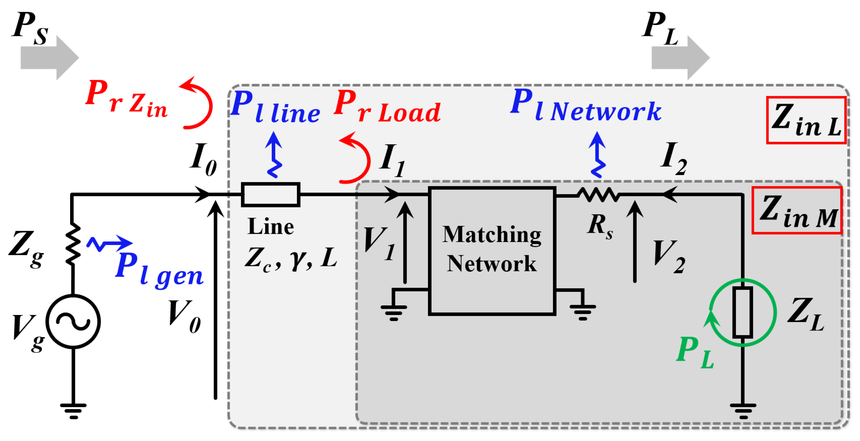
3. Optimal Design of RF Systems Using an Analytical Approach
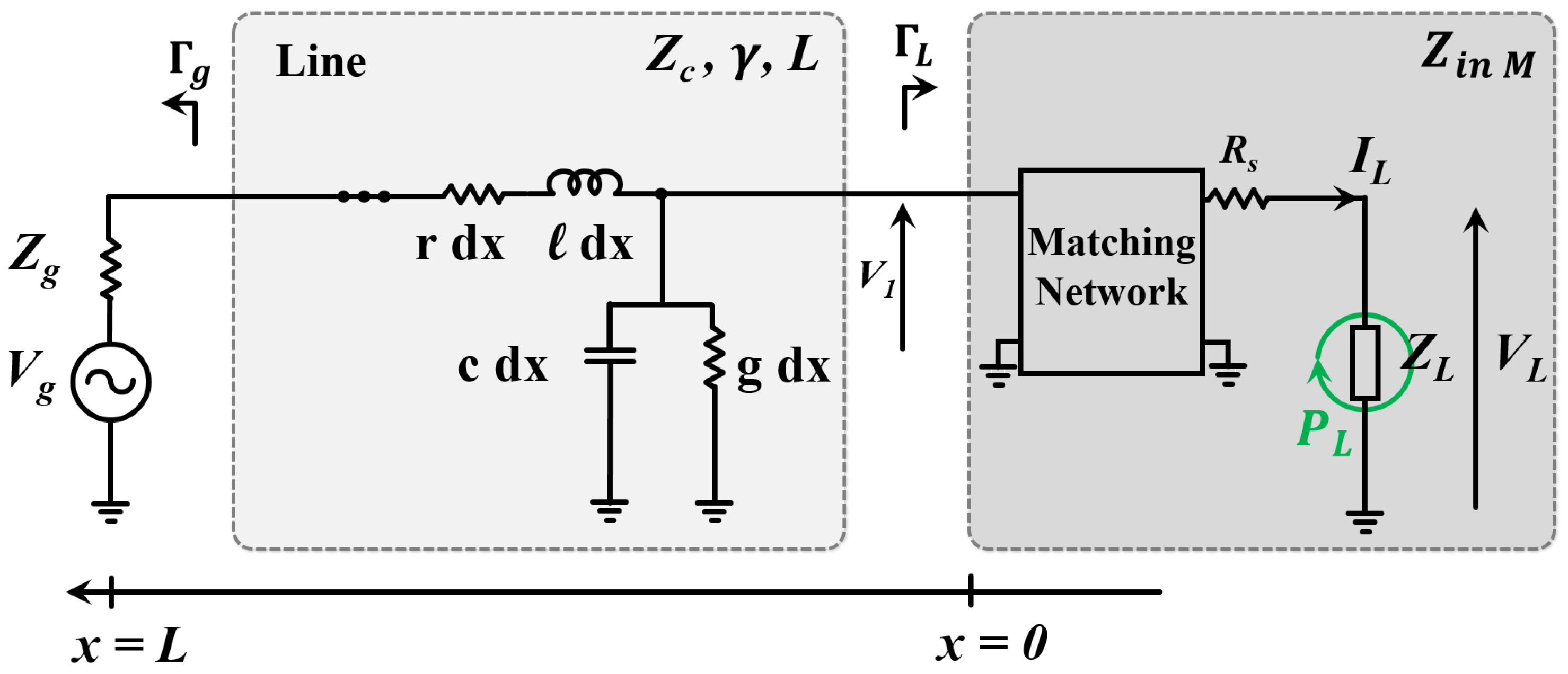
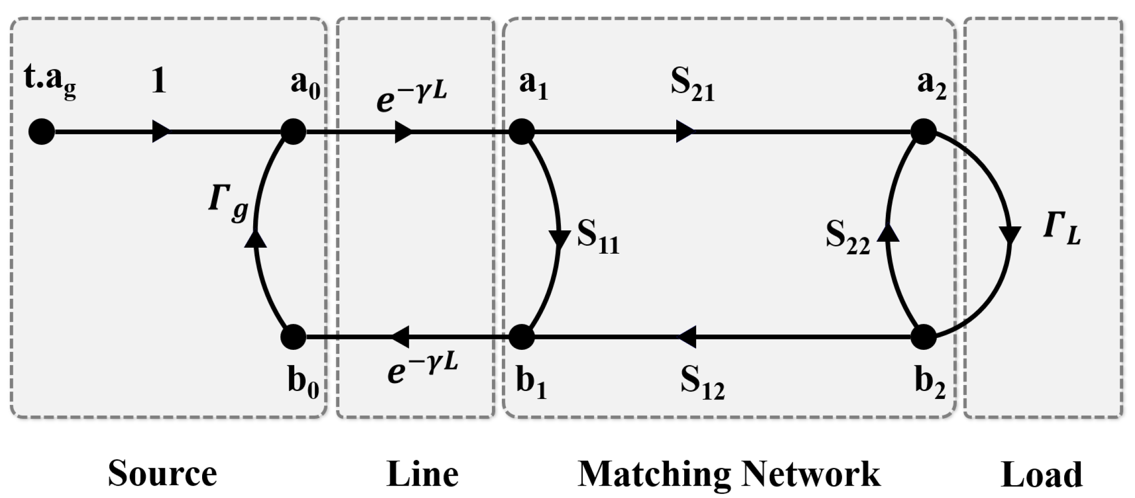
3.1. Integration of the Transmission Line Parameters
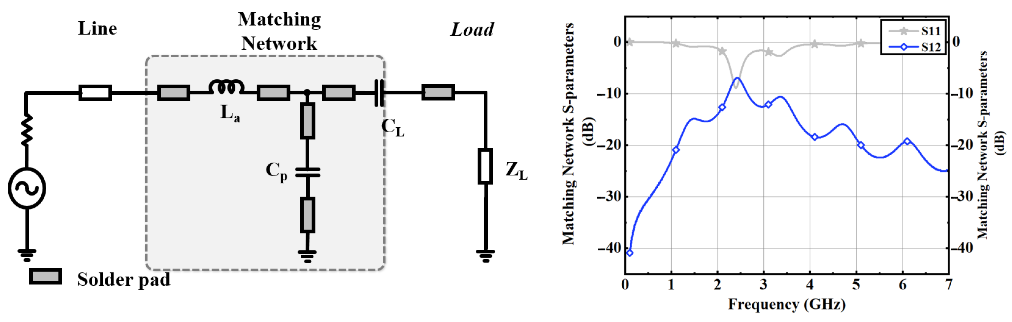
3.2. Integration of Matching Network Parameters
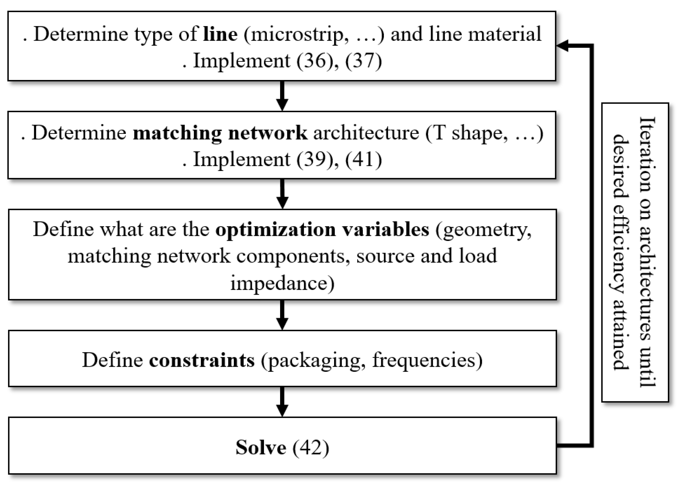
3.3. RF Design Framework
4. Validation and Implementation of the Design Framework
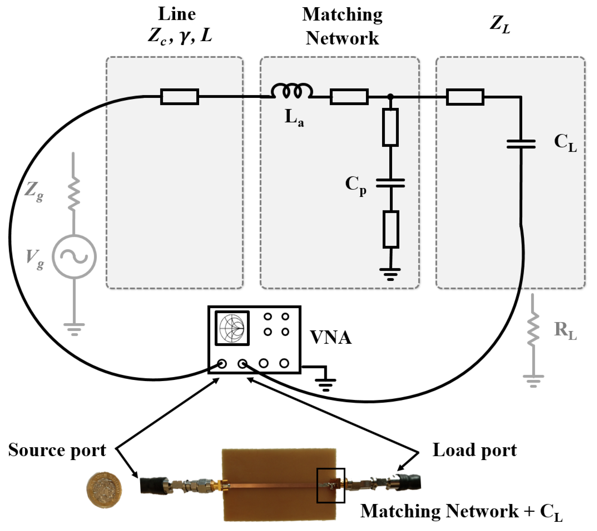
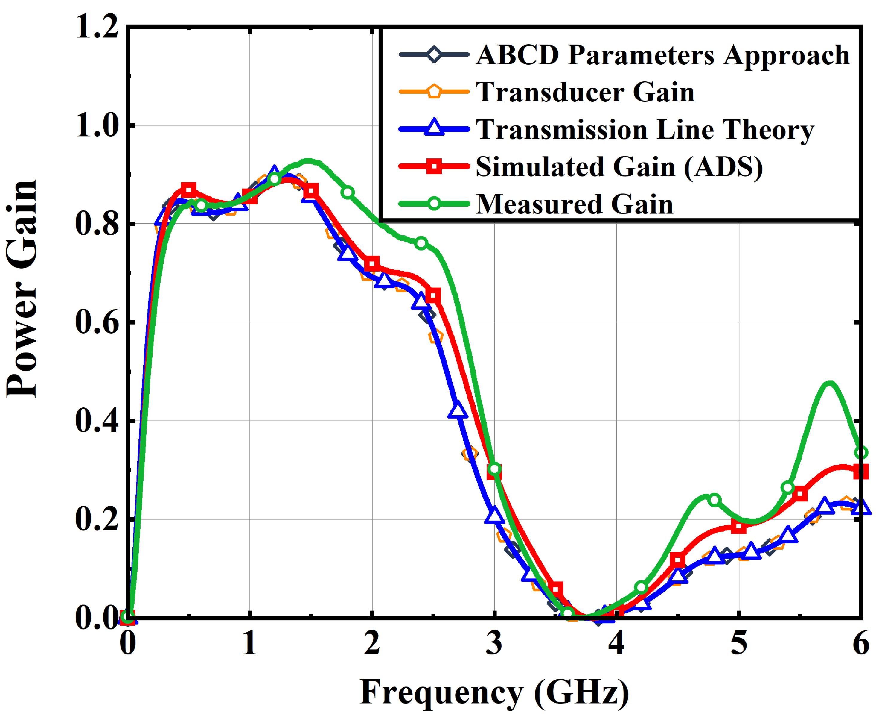
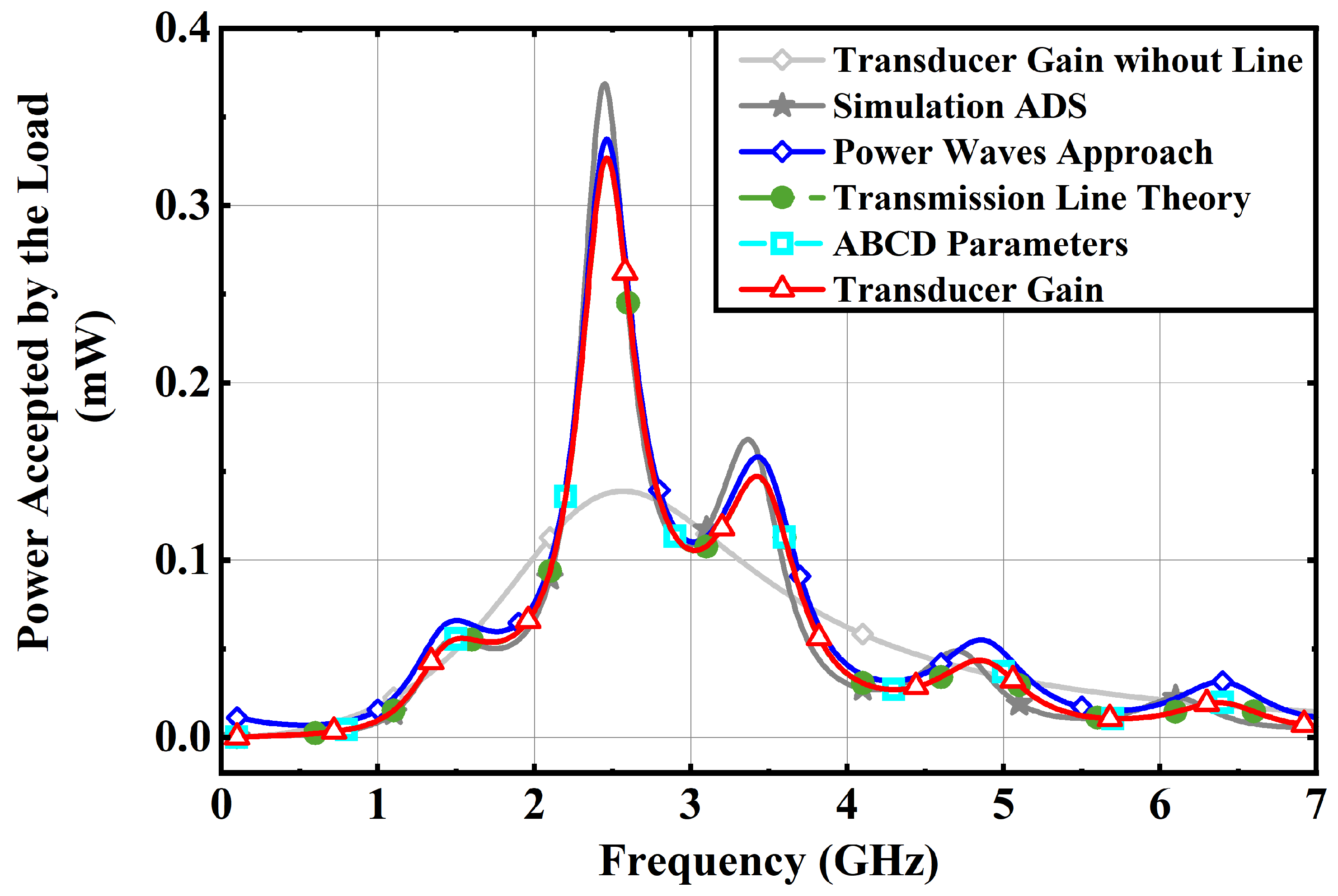
4.1. Validation of Theoretical Approaches
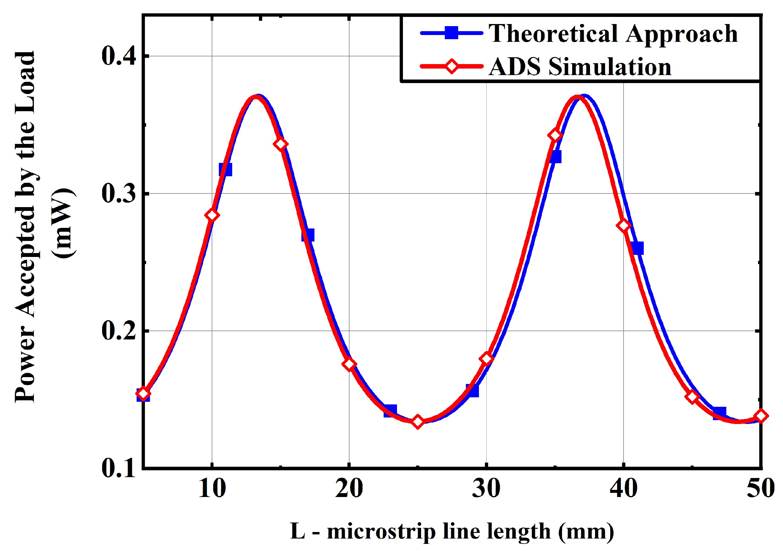
4.2. Implementation of the Proposed Design Framework
5. Conclusions
Funding
Conflicts of Interest
References
- Number of Internet of Things (IoT) Connected Devices Worldwide in 2018, 2025 and 2030. Available online: https://0-www-statista-com.brum.beds.ac.uk/statistics/802690/worldwide-connected-devices-by-access-technology/ (accessed on 30 March 2021).
- Big Data Analytics in the Smart Grid: Big Data Analytics, Machine Learning and Artificial Intelligence in the Smart Grid: Introduction, Benefits, Challenges and Issues, IEEE, United States, WorkingPaper, Nov. 2017, iEEE Smart Grid White Paper. Available online: https://0-smartgrid-ieee-org.brum.beds.ac.uk/images/files/pdf/big_data_analytics_white_paper.pdf (accessed on 30 March 2021).
- Tang, W.; Andoni, M.; Robu, V.; Flynn, D. Accurately forecasting the health of energy system assets. In Proceedings of the 2018 IEEE International Symposium on Circuits and Systems (ISCAS), Florence, Italy, 27–30 May 2018; pp. 1–5. [Google Scholar]
- Tang, W.; Roman, D.; Dickie, R.; Robu, V.; Flynn, D. Prognostics and health management for the optimization of marine hybrid energy systems. Energies 2020, 13, 4676. [Google Scholar] [CrossRef]
- Barnes, M.; Brown, K.; Carmona, J.; Cevasco, D.; Collu, M.; Crabtree, C.; Crowther, C.; Djurovic, S.; Flynn, D.; Green, P.; et al. Technology Drivers in Windfarm Asset Management. Available online: https://researchportal.hw.ac.uk/en/publications/technology-drivers-in-windfarm-asset-management (accessed on 30 March 2021).
- Huynh, N.; Robu, V.; Flynn, D.; Rowland, S.; Coapes, G. Design and demonstration of a wireless sensor network platform for substation asset management. Cired Open Access Proc. J. 2017, 105–108. [Google Scholar] [CrossRef]
- Fisher, M.; Collins, E.; Dennis, L.; Luckcuck, M.; Webster, M.; Jump, M.; Page, V.; Patchett, C.; Dinmohammadi, F.; Flynn, D.; et al. Verifiable self-certifying autonomous systems. In Proceedings of the 2018 IEEE International Symposium on Software Reliability Engineering Workshops (ISSREW), Memphis, TN, USA, 15–18 October 2018; pp. 341–348. [Google Scholar]
- Rana, M.M.; Xiang, W.; Wang, E.; Li, X.; Choi, B.J. Internet of things infrastructure for wireless power transfer systems. IEEE Access 2018, 6, 19295–19303. [Google Scholar] [CrossRef]
- Gurjar, D.S.; Nguyen, H.H.; Tuan, H.D. Wireless information and power transfer for IoT applications in overlay cognitive radio networks. IEEE Internet Things J. 2019, 6, 3257–3270. [Google Scholar] [CrossRef] [Green Version]
- Sheng, Z.; Mahapatra, C.; Zhu, C.; Leung, V.C.M. Recent advances in industrial wireless sensor networks toward efficient management in iot. IEEE Access 2015, 3, 622–637. [Google Scholar] [CrossRef]
- Thingpark Market. Available online: https://market.thingpark.com/ (accessed on 30 January 2021).
- Daskalakis, S.N.; Goussetis, G.; Assimonis, S.D.; Tentzeris, M.M.; Georgiadis, A. A uW backscatter-morse-leaf sensor for low-power agricultural wireless sensor networks. IEEE Sensors J. 2018, 18, 7889–7898. [Google Scholar] [CrossRef] [Green Version]
- Daskalakis, S.; Assimonis, S.D.; Kampianakis, E.; Bletsas, A. Soil moisture scatter radio networking with low power. IEEE Trans. Microw. Theory Tech. 2016, 64, 2338–2346. [Google Scholar] [CrossRef]
- Daskalakis, S.N.; Assimonis, S.D.; Goussetis, G.; Tentzeris, M.M.; Georgiadis, A. The Future of Backscatter in Precision Agriculture. In Proceedings of the IEEE International Symposium on Antennas and Propagation and USNC-URSI Radio Science Meeting, Atlanta, GA, USA, 7–12 July 2019; pp. 647–648. [Google Scholar]
- Zhaksylyk, Y.; Halvorsen, E.; Hanke, U.; Azadmehr, M. Analysis of Fundamental Differences between Capacitive and Inductive Impedance Matching for Inductive Wireless Power Transfer. Electronics 2020, 3, 476. [Google Scholar] [CrossRef] [Green Version]
- Monti, G.; Mastri, F.; Mongiardo, M.; Corchia, L.; Tarricone, L. Transducer gain maximization for a resonant inductive WPT link using relay resonators. In Proceedings of the 2018 IEEE MTT-S International Wireless Symposium (IWS), Chengdu, China, 6–10 May 2018; pp. 1–4. [Google Scholar]
- Vandelle, E.; Bui, D.H.N.; Vuong, T.; Ardila, G.; Wu, K.; Hemour, S. Harvesting ambient RF energy efficiently with optimal angular coverage. IEEE Trans. Antennas Propag. 2019, 67, 1862–1873. [Google Scholar] [CrossRef]
- da Silva, E.F.; Gomes Neto, A.; Peixeiro, C. Fast and accurate rectenna design method. IEEE Antennas Wirel. Propag. Lett. 2019, 18, 886–890. [Google Scholar] [CrossRef]
- Daskalakis, S.N.; Georgiadis, A.; Goussetis, G.; Tentzeris, M.M. A rectifier circuit insensitive to the angle of incidence of incoming waves based on a Wilkinson power combiner. IEEE Trans. Microw. Theory Tech. 2019, 67, 3210–3218. [Google Scholar] [CrossRef]
- Assimonis, S.D.; Daskalakis, S.; Bletsas, A. Sensitive and efficient RF harvesting supply for batteryless backscatter sensor networks. IEEE Trans. Microw. Theory Tech. 2016, 64, 1327–1338. [Google Scholar] [CrossRef] [Green Version]
- Assimonis, S.D.; Daskalakis, S.N.; Fusco, V.; Tentzeris, M.M.; Georgiadis, A. High efficiency RF energy harvester for iot embedded sensor nodes. In Proceedings of the 2019 IEEE International Symposium on Antennas and Propagation and USNC-URSI Radio Science Meeting, Atlanta, GA, USA, 7–12 July 2019; pp. 1161–1162. [Google Scholar]
- Assimonis, S.D.; Fusco, V. RF energy harvesting with dense rectenna-arrays using electrically small rectennas suitable for iot 5G embedded sensor nodes. In Proceedings of the 2018 IEEE MTT-S International Microwave Workshop Series on 5G Hardware and System Technologies (IMWS-5G), Dublin, Ireland, 30–31 August 2018; pp. 1–3. [Google Scholar]
- Couraud, B.; Deleruyelle, T.; Vauche, R.; Flynn, D.; Daskalakis, S.N. A low complexity design framework for nfc-rfid inductive coupled antennas. IEEE Access bf 2020, 8, 111. [Google Scholar] [CrossRef]
- Charthad, J.; Dolatsha, N.; Rekhi, A.; Arbabian, A. System-level analysis of far-field radio frequency power delivery for mm-sized sensor nodes. IEEE Trans. Circuits Syst. Regul. Pap. 2016, 63, 300–311. [Google Scholar] [CrossRef]
- Neubauer, A.; Hammes, M. A digital receiver architecture for Bluetooth in 0.25- μm CMOS technology and beyond. IEEE Trans. Circuits Syst. Regul. Pap. 2007, 54, 2044–2053. [Google Scholar] [CrossRef]
- Oh, S.; Kim, S.; Ali, I.; Nga, T.T.K.; Lee, D.; Pu, Y.; Yoo, S.; Lee, M.; Hwang, K.C.; Yang, Y.; et al. A 3.9 mw bluetooth low-energy transmitter using all-digital PLL-based direct FSK modulation in 55 nm CMOS. IEEE Trans. Circuits Syst. Regul. Pap. 2018, 65, 3037–3048. [Google Scholar] [CrossRef]
- Li, S.C.; Kao, H.-S.; Chen, C.-P.; Su, C.-C. Low-power fully integrated and tunable CMOS RF wireless receiver for ISM band consumer applications. IEEE Trans. Circuits Syst. Regul. Pap. 2005, 52, 1758–1766. [Google Scholar] [CrossRef]
- Xu, K. Integrated silicon directly modulated light source using p-well in standard cmos technology. IEEE Sensors J. 2016, 16, 6184–6191. [Google Scholar] [CrossRef]
- Shafiee, N.; Tewari, S.; Calhoun, B.; Shrivastava, A. Infrastructure circuits for lifetime improvement of ultra-low power IoT devices. IEEE Trans. Circuits Syst. Regul. Pap. 2017, 64, 2598–2610. [Google Scholar] [CrossRef]
- Zeng, W.; Ren, Y.; Lam, C.; Sin, S.; Che, W.; Ding, R.; Martins, R.P. A 470-nA quiescent current and 92.7 control buck converter with seamless mode selection for IoT application. IEEE Trans. Circuits Syst. Regul. Pap. 2020, 1–14. [Google Scholar] [CrossRef]
- Assimonis, S.; Fusco, S.; Georgiadis, A.; Samaras, T. Efficient and sensitive electrically small rectenna for ultra-low power RF energy harvesting. Sci. Rep. 2018, 8. [Google Scholar] [CrossRef] [Green Version]
- Sheng, W.; Emira, A.; Sanchez-Sinencio, E. CMOS RF receiver system design: A systematic approach. IEEE Trans. Circuits Syst. Regul. Pap. 2006, 53, 1023–1034. [Google Scholar] [CrossRef] [Green Version]
- Ivrlac, M.T.; Nossek, J.A. Toward a circuit theory of communication. IEEE Trans. Circuits Syst. Regul. Pap. 2010, 57, 1663–1683. [Google Scholar] [CrossRef]
- Vasjanov, A.; Barzdenas, V. A methodology improving off-chip, lumped RF impedance matching network response accuracy. Electronics 2018, 7, 188. [Google Scholar] [CrossRef] [Green Version]
- Rathod, V. A Review of Electric Impedance Matching Techniques for Piezoelectric Sensors, Actuators and Transducers. Electronics 2019, 2, 169. [Google Scholar] [CrossRef] [Green Version]
- Thompson, M.; Fidler, J.K. Determination of the impedance matching domain of impedance matching networks. IEEE Trans. Circuits Syst. Regul. Pap. 2004, 51, 2098–2106. [Google Scholar] [CrossRef]
- Chappidi, C.R.; Sengupta, K. Globally optimal matching networks with lossy passives and efficiency bounds. IEEE Trans. Circuits Syst. Regul. Pap. 2018, 65, 257–269. [Google Scholar] [CrossRef]
- Wu, Y.; Jiao, L.; Liu, Y. Comments on ’novel dual-band matching network for effective design of concurrent dual-band power amplifiers. IEEE Trans. Circuits Syst. Regul. Pap. 2015, 62, 2361–2363. [Google Scholar] [CrossRef]
- Sjoblom, P.; Sjoland, H. An adaptive impedance tuning CMOS circuit for ism 2.4-ghz band. IEEE Trans. Circuits Syst. Regul. Pap. 2005, 52, 1115–1124. [Google Scholar] [CrossRef]
- Hur, B.; Eisenstadt, W.; Melde, K. Testing and validation of adaptive impedance matching system for broadband antenna. Electronics 2019, 8, 1055. [Google Scholar] [CrossRef] [Green Version]
- Bodway, G. Two port power flow analysis using generalized scattering parameters. In Microwave Journal; Horizon House Publications: Norwood, MA, USA, 1967. [Google Scholar]
- Pozar, D.M. Microwave engineering; Wiley: Hoboken, NJ, USA, 2012; ISBN 978-0-470-63155-3. [Google Scholar]
- Kurokawa, K. Power waves and the scattering matrix. IEEE Trans. Microw. Theory Tech. 1965, 13, 194–202. [Google Scholar] [CrossRef] [Green Version]
- Finkenzeller, K. RFID Handbook: Fundamentals and Applications in Contactless Smart Cards, Radio Frequency Identification and near-Field Communication; John Wiley and Sons: Hoboken, JK, USA, 2010. [Google Scholar]
- Frickey, D.A. Conversions between s, z, y, h, abcd, and t parameters which are valid for complex source and load impedances. IEEE Trans. Microw. Theory Tech. 1994, 42, 205–211. [Google Scholar] [CrossRef]
- Baudin, P. Wireless transceiver architecture: Bridging RF and digital communications; Wiley: Hoboken, NJ, USA, 2014; ISBN 978-1-118-87482-0. [Google Scholar]
- Sadiku, M. Elements of Electromagnetics; Oxford University Press: Oxford, UK, 2014. [Google Scholar]
- Denlinger, E.J. Losses of microstrip lines. IEEE Trans. Microw. Theory Tech. 1980, 28, 513–522. [Google Scholar] [CrossRef]
- Chang, K. Handbook of Microwave and Optical Components, Microwave Passive and Antenna Components; ser. Handbook of Microwave and Optical Components; Wiley: Hoboken, NJ, USA, 1989. [Google Scholar]
- Matthaei, G. Microwave Filters, Impedance-Matching Networks, and Coupling Structures; McGraw-Hill: New York, NY, USA, 1964. [Google Scholar]
- Ferrero, A.; Pirola, M. Harmonic load-pull techniques: An overview of modern systems. IEEE Microw. Mag. 2013, 14, 116–123. [Google Scholar] [CrossRef]
- Angelotti, A.M.; Gibiino, G.P.; Nielsen, T.S.; Schreurs, D. Santarelli, A. Wideband active load-pull by device output match compensation using a vector network analyzer. IEEE Trans. Microw. Theory Tech. 2021, 69, 874–886. [Google Scholar] [CrossRef]
- Couraud, B.; Deleruyelle, T.; Kussener, E.; Vauche, R. Real-time impedance characterization method for rfid-type backscatter communication devices. IEEE Trans. Instrum. Meas. 2018, 67, 288–295. [Google Scholar] [CrossRef]
- Michalewicz, Z.; Schoenauer, M. Evolutionary algorithms for constrained parameter optimization problems. Evol. Comput. 1996, 4, 1–32. [Google Scholar] [CrossRef]
- Cihangir, A.; Panagamuwa, C.J.; Whittow, W.G.; Jacquemod, G.; Gianesello, F.; Pilard, R.; Luxey, C. Dual-band 4G eyewear antenna and sar implications. IEEE Trans. Antennas Propag. 2017, 65, 2085–2089. [Google Scholar] [CrossRef] [Green Version]
- Zheng, Y.F.; Sun, G.H.; Huang, Q.K.; Wong, S.W.; Zheng, L.S. Wearable PIFA antenna for smart glasses application. In Proceedings of the 2016 IEEE International Conference on Computational Electromagnetics (ICCEM), Guangzhou, China, 23–25 February 2016; pp. 370–372. [Google Scholar]


| Approach Name Name | Strengths | Weakness of Usual Use Case |
|---|---|---|
| ABCD parameters | Multiplication of matrices that depend on system’s impedances | None |
| Transducer gain | Expressed as a function of scattering parameters | Does not include transmission line |
| Transmission lines theory | Simple formula models the effects of the line | Expression depends on unknown parameters ( in (24)) |
| Power waves | Simple formula | Does not include transmission line nor matching network |
| Parameter | Value | Unit | Parameter | Value | Unit |
|---|---|---|---|---|---|
| 50 | d | 1.5 | mm | ||
| 50 | 1 | nH | |||
| w | 2.3 | mm | 1 | pF | |
| h | 1.6 | mm | 10 | pF | |
| L | 67 | mm | 4.4 |
| Parameter | Value | Unit | Parameter | Value | Unit |
|---|---|---|---|---|---|
| 75 | 5.7 | nH | |||
| 72 | 0.6 | pF | |||
| w | 2.1 | mm | 0.1 | pF | |
| h | 1.6 | mm | 9.6 | ||
| L | 37 | mm |
Publisher’s Note: MDPI stays neutral with regard to jurisdictional claims in published maps and institutional affiliations. |
© 2021 by the authors. Licensee MDPI, Basel, Switzerland. This article is an open access article distributed under the terms and conditions of the Creative Commons Attribution (CC BY) license (https://creativecommons.org/licenses/by/4.0/).
Share and Cite
Couraud, B.; Vauche, R.; Daskalakis, S.N.; Flynn, D.; Deleruyelle, T.; Kussener, E.; Assimonis, S. Internet of Things: A Review on Theory Based Impedance Matching Techniques for Energy Efficient RF Systems. J. Low Power Electron. Appl. 2021, 11, 16. https://0-doi-org.brum.beds.ac.uk/10.3390/jlpea11020016
Couraud B, Vauche R, Daskalakis SN, Flynn D, Deleruyelle T, Kussener E, Assimonis S. Internet of Things: A Review on Theory Based Impedance Matching Techniques for Energy Efficient RF Systems. Journal of Low Power Electronics and Applications. 2021; 11(2):16. https://0-doi-org.brum.beds.ac.uk/10.3390/jlpea11020016
Chicago/Turabian StyleCouraud, Benoit, Remy Vauche, Spyridon Nektarios Daskalakis, David Flynn, Thibaut Deleruyelle, Edith Kussener, and Stylianos Assimonis. 2021. "Internet of Things: A Review on Theory Based Impedance Matching Techniques for Energy Efficient RF Systems" Journal of Low Power Electronics and Applications 11, no. 2: 16. https://0-doi-org.brum.beds.ac.uk/10.3390/jlpea11020016