Article

A 0.3 V Rail-to-Rail Ultra-Low-Power OTA with Improved Bandwidth and Slew Rate

by
Francesco Centurelli
,
Riccardo Della Sala
,
Pietro Monsurrò
,
Giuseppe Scotti
* and
Alessandro Trifiletti
Dipartimento di Ingegneria dell’Informazione, Elettronica e Telecomunicazioni (DIET), Università di Roma La Sapienza, 00184 Roma, Italy
*
Author to whom correspondence should be addressed.
J. Low Power Electron. Appl. 2021, 11(2), 19; https://0-doi-org.brum.beds.ac.uk/10.3390/jlpea11020019
Submission received: 26 March 2021 / Revised: 14 April 2021 / Accepted: 18 April 2021 / Published: 21 April 2021

Abstract

:
In this paper, we present a novel operational transconductance amplifier (OTA) topology based on a dual-path body-driven input stage that exploits a body-driven current mirror-active load and targets ultra-low-power (ULP) and ultra-low-voltage (ULV) applications, such as IoT or biomedical devices. The proposed OTA exhibits only one high-impedance node, and can therefore be compensated at the output stage, thus not requiring Miller compensation. The input stage ensures rail-to-rail input common-mode range, whereas the gate-driven output stage ensures both a high open-loop gain and an enhanced slew rate. The proposed amplifier was designed in an STMicroelectronics 130 nm CMOS process with a nominal supply voltage of only 0.3 V, and it achieved very good values for both the small-signal and large-signal Figures of Merit. Extensive PVT (process, supply voltage, and temperature) and mismatch simulations are reported to prove the robustness of the proposed amplifier.

1. Introduction

The development of ultra-low-power (ULP) and ultra-low-voltage (ULV) integrated circuits is driven by applications such as the Internet of Things (IoT) [1,2,3,4] and implanted biomedical devices [5,6,7,8]. The number of IoT devices connected to the internet for gathering and processing information is increasing at a faster and faster rate. The enormous number of connected devices and the fact that they are often battery powered or must scavenging energy from the environment make low power consumption a key feature in IoT devices [1]. Therefore, the design of integrated circuits (ICs) for IoT applications is becoming more and more difficult due to the stringent constraints in terms of power dissipation, minimum supply voltage, and area footprint [1,2]. Due to the above constraints and the low intrinsic gain of nanometer MOS transistors, analog interfaces are, in many cases, the most challenging building blocks of ICs for IoT applications [2,3].
In the context of implanted biomedical applications, front-end amplifiers for neural recording systems often rely on AC coupling with cutoff frequencies below 1 Hz to eliminate the DC offset of the electrodes and to properly process the neural signals [5,6]. Such devices are usually designed for different frequency slots in the range from 1 Hz to 10 kHz. For example, in the case of epileptic seizure detection, band-pass filters in the range of 250 to 500 Hz are required to extract the signals of interest. Low-voltage operation, low power consumption, and a small silicon area are the main requirements of ICs for these systems [7,8].
ULP and ULV operational transconductance amplifiers (OTAs) are key components for both the IoT and implanted biomedical devices, and a huge number of OTAs have been presented in recent years [9]. In [10], Stockstad et al. presented a 0.9 V operational amplifier that, for the first time, exploited the bulk-driven technique to attain rail-to-rail input–output swing. Over the years, the research community has increasingly focused on reducing the supply voltage and power consumption at the expense of common-mode rejection ratio (CMRR) performance [11,12,13,14]. Several common-mode feedback (CMFB) approaches, which exploit triode-biased devices or current cancellation, have been proposed with the aim of minimizing the common-mode gain in fully differential OTAs, thus improving their CMRR performance [15,16,17,18,19].
Multi-stage OTAs based on folded cascode or gain-boosting topologies and with supply voltages in the range from 0.6 to 0.9 V have been presented in the literature [20,21,22,23,24]. However, when targeting supply voltages lower than 0.4 V, the adoption of the topologies and design strategies reported above is no longer possible, and pseudo-differential or inverter-based architectures are often used [25,26,27,28,29,30,31,32]. In fact, at these supply voltages, gate-driven amplifiers are not adequate for ensuring a rail-to-rail input common-mode range (ICMR). However, due to the lack of tail current generators, pseudo-differential and inverter-based circuits typically exhibit a not-well-defined bias point and a poor CMRR, and body bias strategies are less effective due to the limited available voltage swing on body terminals.
ULV circuits can employ floating gate devices [33] or body-driven stages [34,35] to increase the input common-mode swing. Body-driven input stages are inherently rail-to-rail in ULV applications, and forward biasing of the NP junctions is not a concern when supply voltages are lower than about 0.6 V. Unlike gate-driven stages, however, they tend to have higher noise, lower bandwidth, and resistive input impedance. Despite these shortcomings, there is no alternative at supply voltages around 0.3 V if a large common-mode input signal swing is desired. Furthermore, the gate terminals of the input devices can be used for biasing, the biasing current of the amplifiers can be accurately set, and pseudo-differential architectures can even be exploited.
Additional interesting OTA architectures based on fully digital operation were recently proposed in [36,37], which showed the feasibility of full standard-cell-based analog amplifiers.
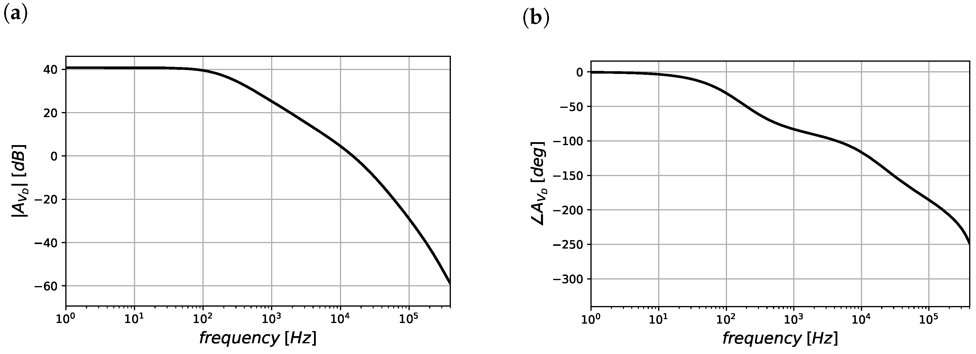
In addition to gain and robustness considerations, ULP and ULV topologies may have low bandwidth (because of sub-threshold biasing) and poor slew-rate performance (because of low biasing currents). Hence, it is important to assess the OTA performance in terms of bandwidth and slew rate for a given current or power consumption and capacitive load, which refer to the popular large-signal and small-signal Figures of Merit (FOMs).
In this paper, we present a novel OTA topology based on a body-driven input stage with a dual path to improve CMRR that exploits body-driven current mirror load for differential-to-single-ended conversion at the output. The proposed OTA has only one high-impedance node, and can therefore be compensated at the output stage, thus avoiding Miller compensation. The body-driven input stage ensures the rail-to-rail input common-mode range, whereas the coupling between the first and second stages and the gate-driven output stage ensure high open-loop gain and good slew-rate performance.
The paper is organized as follows: Section 2 describes the proposed topology; Section 3 analyzes the small-signal and large-signal circuit responses, including the CMRR; Section 4 reports the design and simulation results, with emphasis on the process, supply voltage, and temperature (PVT) variations, as well as on stochastic mismatch variations; a comparison with the related literature to highlight the advantages of the proposed topology in terms of the FOMs is also presented in Section 4. Finally, the conclusions are reported in Section 5.

2. Proposed Topology

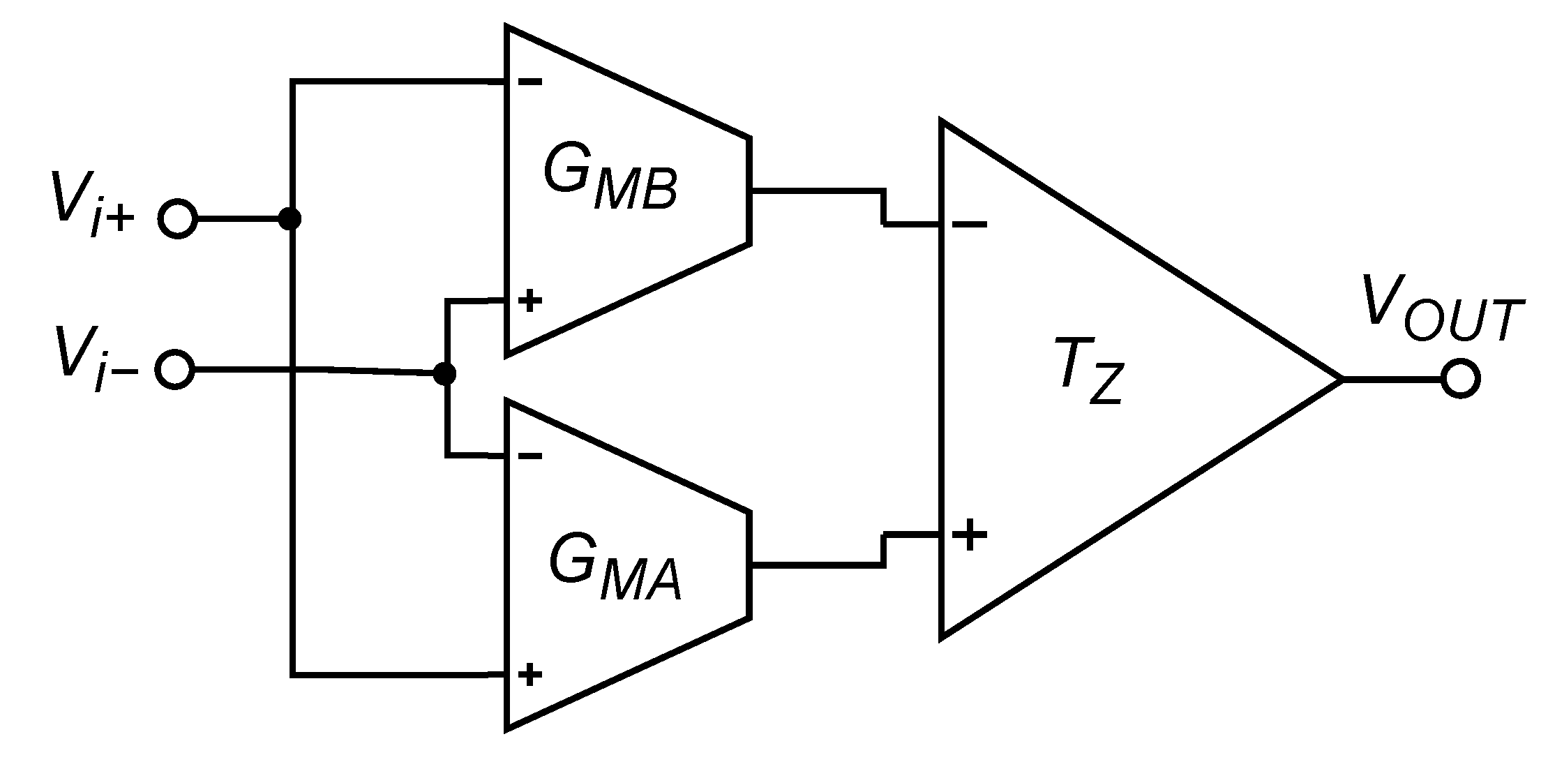
The block scheme of the proposed OTA is reported in Figure 1, showing the usage of two matched transconductors G M A and G M B , whose output currents are sent to a transimpedance stage T Z , in which the common-mode currents are ideally cancelled, and the differential currents are summed to double the transconductance gain. 
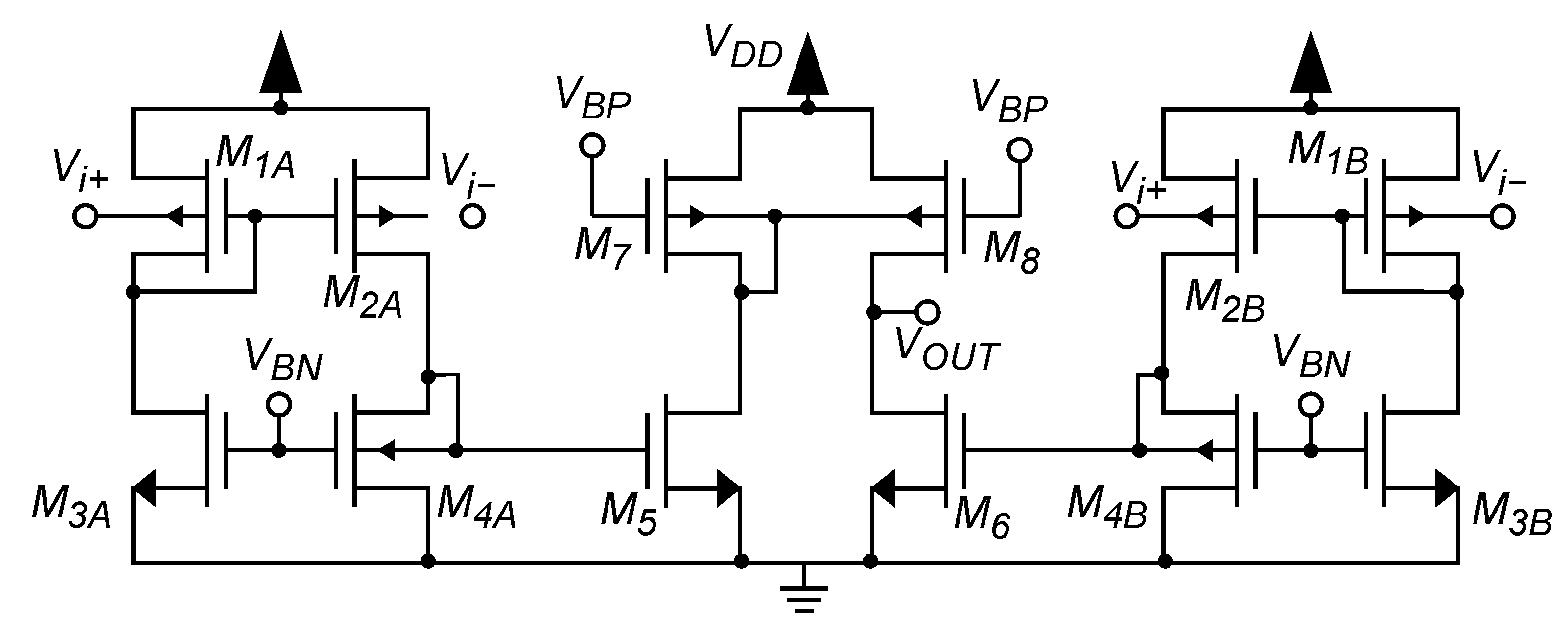
Figure 2 shows the detailed schematic of the OTA. Transistors M 1 A , M 2 A , M 3 A and M 1 B , M 2 B , M 3 B form the two input transconductance stages, which are shown in Figure 1 as G M A and G M B . The second stage of the OTA is made up of transistors M 4 A , M 4 B , M 5 , M 6 , M 7 , M 8 , which implement the transimpedance stage T Z shown in Figure 1.
To allow rail-to-rail input swing, a body-driven first stage is used. Due to the ULV supply, particular care was taken to identify a biasing strategy that was able to guarantee robustness with respect to the PVT and mismatch variations. In fact, since each transistor requires a minimum V d s to properly operate, tail current generators are not an option, and the lack of tail current generators reduces common-mode rejection. Hence, the dual transconductance path in the input stage was exploited to guarantee high CMRR under the hypothesis of well-matched transconductances. Furthermore, since M 1 A , B and M 2 A , B comprise a current mirror and M 3 A , B acts as a current source, a well-defined bias current is obtained. It has to be noted that the two transconductors G M A and G M B have to be designed symmetrically and must be well matched with each other in order to optimize common-mode cancellation. The second stage of the OTA exploits two body-diode NMOSs, so the input impedance is equal to 1 / g m b . Transistors M 4 A , M 5 and M 4 B , M 6 act as current amplifiers. The gates of transistors M 7 and M 8 determine the biasing current of the second stage. The body-driven current mirror M 7 and M 8 provides differential-to-single-ended conversion and allows further rejection of the common-mode current component, since the common-mode current in M 6 and M 8 is the same. The output conductance g d s 8 + g d s 6 of the stage provides voltage gain to the amplifier.
It has to be noted that the differential input stage is very similar to the one used in [35,38,39]. However, in these works, the transconductors G M A and G M B are loaded by a conventional gate-driven current mirror, which performs the differential-to-single-ended conversion in the first stage. The first stage is then followed by one or two stages with Miller or Nested Miller compensation. In the proposed circuit, instead, the transconductors G M A and G M B are loaded by a differential body-diode load, and therefore, the input stage can be considered as a fully differential amplifier. The second stage of the proposed topology can be seen as a pseudo-differential pair loaded with a body-driven current mirror that performs the differential-to-single-ended conversion at the output, thus further increasing the CMRR and avoiding Miller compensation. The relatively high CMRR is obtained as a combination of two kinds of effects: the intrinsic CMRR of the simple differential pairs M1A-M3A and M1B-M3B, as explained in [38], and trough symmetry and cancellation of currents due to the body-driven current mirror in the output stage.

3. Circuit Analysis

In this section, we present a small-signal and large-signal analysis of the proposed amplifier, including the frequency response, the CMRR, and the slew-rate performance.

3.1. Differential Gain Frequency Response

Referring to the block scheme in Figure 1, the differential gain of the proposed OTA can be easily computed as:
A V D = 2 · G M A ( B ) · T Z
where G M A ( B ) is the transconductance gain of the first stage and T Z is the transimpedance gain of the second stage. To calculate the gains, we refer to the detailed schematic in Figure 2 and denote with subscript p 1 the small-signal parameters of M 1 A M 1 B M 2 A M 1 B , with subscript n 1 the small-signal parameters of M 3 A M 3 B M 4 A M 4 B , with subscript n 2 the parameters of M 5 and M 6 , and with subscript p 2 those of M 7 and M 8 . Note that we have exploited both the symmetry of the matched devices and the identity of their bias point due to the appropriate sizing of the devices.
Therefore:
g m 1 A ( B ) = g m 2 A ( B ) = g m p 1 ; g m b 1 A ( B ) = g m b 2 A ( B ) = g m b p 1 ;
g m b 4 A ( B ) = g m b n 1 ; g m b 7 ( 8 ) = g m b p 2 ;
g m 5 ( 6 ) = g m n 2 ;
C g s 1 A ( B ) = C g s 2 A ( B ) = C g s p 1 ; C g s 5 ( 6 ) = C g s n 2 ;
and under the hypotheses that
g d s 1 A ( B ) + g d s 2 A ( B ) < < g m 1 A ( B )
C g d 2 A ( B ) < < C g s 1 A ( B ) + C g s 2 A ( B )
G M A ( B ) can be calculated as:
G M A ( B ) = g m b p 1 · 1 + s C g s p 1 g m p 1 1 + s 2 C g s p 1 g m p 1
Since the ratio between the pole and the zero in the above equation is 2 and because they are at a high frequency, the effect of the pole–zero doublet can usually be neglected.
Now, focusing on the second stage, the transimpedance gain T z can be expressed as:
T z = g m n 2 g m b n 1 g d s n 2 + g d s p 2 · 1 s C g d n 2 g m n 2 1 + s p 1 1 + s p 2
where p 1 and p 2 are respectively equal to:
p 1 = g d s n 2 + g d s p 2 C L
p 2 = g m b n 1 C g s n 2
In Equation (9), we neglect the effect of the pole–zero doublet of the current mirror M 7 M 8 , analogously to the one in Equation (8), and that of the mirror M 4 A M 5 ( M 4 B M 6 ), since they have a negligible impact on the frequency response. In addition, the additional pole–zero doublets were neglected due to transistors M 4 A ( B ) and M 5 ( 6 ) , thus introducing a limited error in the frequency response derivation.
Now, we focus on the DC differential gain, which can be expressed as:
A V D = 2 · g m b p 1 g m b n 1 · g m n 2 g d s n 2 + g d s p 2
Considering Equations (8) and (9), it is clear that the dominant pole is given by the output impedance g d s 8 + g d s 6 , whereas the poles and zeros proportional to g m b i or g m i are positioned at a higher frequency. Therefore, the GBW can be easily derived as:
G B W = A V D · p 1 2 π = 1 π g m b p 1 g m b n 1 · g m n 2 C L

3.2. Common-Mode Gain

The common-mode gain was estimated under the hypothesis of there being no mismatch between the two input transconductors (i.e., G M A = G M B ).
According to these approximations and to Equation (3), the common-mode gain can be written as:
A V C = g m n 2 α 1 + α · g m b p 1 g m b n 1 · β 1 + β · γ 1 + γ · 1 g d s n 2 + g d s p 2
where α depends on the M 1 M 2 current mirror:
α = g d s n 1 + g d s p 1 g m n 1
β is defined as:
β = g d s n 1 + g d s p 1 g m b p 1
and the third term γ depends on the M 7 M 8 mirror:
γ = 2 · g d s p 2 g m b p 2
The factors in Equations (15)–(17) are inversely proportional to g m / g d s (the intrinsic gain of the device) or g m b / g d s (the intrinsic gain when driven by the body terminal). Equation (14) thus shows that, for the ideal case of infinite output resistance (infinite intrinsic gain), the common-mode gain would be zero. This is, however, not the case for deep submicron devices, which present a limited intrinsic gain; thus, the gain in Equation (15) is not negligible. Equations (13)–(15) allow the calculation of the CMRR as:
C M R R = 2 1 + 1 α 1 + 1 β 1 + 1 γ

3.3. Noise Analysis

The noise analysis of the amplifier can be performed by considering a current noise generator between the drain and source terminals for each device. The generator includes both thermal channel noise and flicker noise; thus, its power spectral density can be expressed with Equation (19):
I n ( p ) d = I n ( p ) w + I n ( p ) f
where:
i n ( p ) w 2 ¯ = 4 k T n n ( p ) γ g m i 2 q I d
i n ( p ) f 2 ¯ = K n ( p ) f C o x g m 2 W L
The equivalent input noise voltage can be derived by calculating the output voltage due to the noise sources and dividing it by the differential gain in Equation (12).
v e q 2 ¯ = i n 1 2 ¯ + i p 1 2 ¯ g m b p 1 2 + g m b n 1 2 2 g m b p 1 2 g m n 2 2 i n 2 2 ¯ + i p 2 2 ¯
The resulting power spectral density can be expressed as Equation (22), where the noise spectra i n ( p ) i 2 ¯ (i = 1, 2) represent the noise spectra of i-th NMOS or PMOS stage.
Therefore, Equation (22) shows that the main noise contributions are due to the input stages of N(P)MOS, as can be expected. However the body-driven stage rejects the noise contributions less efficiently than the gate-driven ones. Thus, a larger device size must be chosen to achieve the same noise performance.

3.4. Large-Signal Analysis

The amplifier was optimized for large-signal performance by exploiting class AB behavior. Indeed, the first-stage output current is not limited by the M 3 ( A , B ) bias current I b i a s , but by the voltage swing on the input body terminals. The output terminal of the first stage can thus practically reach the supply voltage V D D . Therefore, the current in the output stage is also not limited by the bias current, but by the maximum V g s of M 5 and M 6 . To be more precise, the negative slew rate is limited by the gate voltage of M 6 reaching the supply voltage. On the other hand, the maximum current of M 8 is limited by the available voltage swing of the body terminal of M 7 and M 8 , thus resulting in a slightly asymmetrical slew rate. The positive and negative slew rates are respectively equal to:
S R + = I d 0 C L · W 8 L 8 · exp α V D D V t h p 0 V g s q 8 n U T
and
S R = I d 0 C L · W 6 L 6 · exp V D D V t h n n U T
where V t h p 0 represents the absolute value of the threshold voltage when V s b is equal to 0. On the other hand, in Equation (24), the V t h n represents the NMOS threshold voltage at the selected V b s n .

4. Amplifier Design and Simulation Results

The proposed amplifier was designed with the 130 nm STMicroelectronics CMOS technology and simulated within the Cadence Virtuoso environment.

4.1. Sizing

To achieve the minimum power consumption with a supply voltage V d d - V s s of only 0.3 V and | V t h | 0.35 V, all devices were biased in the sub-threshold region, and | V d s | and | V g s | were equal to 150 mV. A load capacitance C L of 40 pF was assumed in reference to a typical IoT sensor interface application [16,40,41,42,43].
Large transistor widths and lengths were used to reduce the contributions of thermal and flicker noise, which represent a crucial issue in body-driven amplifiers [21,39,44]. In fact, larger devices have lower narrow- and short-channel effects, lower flicker noise, and larger body transconductance, which are useful for ULV and ULP applications. The bias current of the two symmetrical stages G M A and G M B was set to 13.1 nA as a tradeoff between noise and power consumption. The bias current of the second stage was set to about 95 nA as a tradeoff between slew rate, GBW, and phase margin for the assigned load capacitance. The sizing of the MOS transistors and their small-signal parameters are reported in Table 1.

4.2. Circuit Simulations

The results of the open-loop AC simulations of the proposed OTA are reported in Figure 3 and Figure 4. In particular, Figure 3 shows that the amplifier attains an overall DC gain and GBW of about 40 dB and 18.65 kHz, respectively, as expected from the model in Equations (12) and (13). Furthermore, as previously mentioned, the pole–zero doublets have a marginal effect on the amplifier frequency response. The positive zero g m n 2 / C g d n 2 is at a much greater frequency than the poles p 1 and p 2 , and is therefore negligible. The phase margin (m φ ) of the amplifier is set with the position of pole p 2 with respect to the unity gain frequency: the transistor sizing reported in Table 1 results in m φ = 52°. Figure 4 shows the CMRR of the amplifier, which resulted in about 67 dB.
The amplifier was then simulated in a non-inverting buffer configuration, as shown in Figure 5a. The closed-loop frequency response of the OTA is depicted in Figure 5b, whereas the DC transfer characteristics are shown in Figure 6a, which highlights a rail-to-rail behavior. Figure 6b shows the dependence of the first-stage bias current when the amplifier is excited with a rail-to-rail signal. The positive and negative slew rates of the proposed amplifier were simulated with a full-swing input square wave. Figure 7a shows the time-domain response of the non-inverting buffer in the slew-rate test. The positive and negative slew rates are S R + = 10.83 V/ms and S R = 32.37 V/ms, respectively, and are thus in good agreement with Equations (23) and (24). The simulation results validate the preliminary analysis. The total harmonic distortion (THD) was simulated for different values of the peak-to-peak amplitude of a sinusoidal wave as the input, and is plotted in Figure 7b, which shows a THD lower than 1% for peak-to-peak amplitudes lower than about 230 mV. The plot of the power supply rejection ratio (PSRR) as a function of frequency is reported in Figure 8a, which shows a PSRR of about 45 dB at low frequencies.
Figure 8b reports the input-referred noise plot of the proposed OTA, which shows a noise corner frequency of about 1 kHz and an input-referred noise at f n c of about 2.1 μ V/ H z .

4.3. Robustness to Mismatch and PVT Variations

The robustness of the amplifier to device mismatches was validated through Monte Carlo simulations, whose results are summarized in Table 2. The results are consistent with those of typical simulations. However, mismatches negatively affect the CMRR of the amplifier, as it strongly depends on the matching between two symmetrical paths. The Monte Carlo simulations still show a CMRR of about 52 dB, which is a good result considering the low supply voltage and the lack of tail generators. The amplifier area amounts to about 0.0036 μ m 2 , and it was estimated with the aid of Cadence Layout XL. Additionally, the amplifier performances were also validated using PVT variations. The amplifier shows a good stability with ±10% supply voltage variations, as shown in Table 3.
It has to be pointed out that the proposed topology can work at higher supply voltages provided that the circuit is properly resized according to the main guidelines reported at the beginning of this section (e.g., | V d s | and | V g s | are equal to half of | V d d - V s s | ). As a confirmation, we successfully resized the circuit to operate at 0.4 V, thus obtaining an improvement of about 12 dB in the DC gain. If a supply voltage in the range of 0.6 V is available, the topology can still work, but in this case, it would be preferable to add cascode MOS devices in order to keep the devices in the sub-threshold and to achieve a much larger DC gain.
Table 4 reports the performance of the OTA as a function of the operating temperature, showing that the amplifier is robust in a range of [−10, 80] °C, whereas at higher temperatures, the performances exhibit larger variations. However, if needed, the effects of temperature variations could be mitigated by exploiting PTAT (proportional to absolute temperature) current sources.

4.4. Results and Comparison with the Literature

In Table 5, the proposed amplifier is compared to other ULV–ULP topologies from the literature. To fairly compare the performance of different designs, we considered the following well-known small-signal and large-signal FOMs:
I F O M S = G B W · C L I T O T
I F O M L = S R A V G · C L I T O T
F O M S = G B W · C L P D I S S
F O M L = S R A V G · C L P D I S S
The small-signal FOMs (25) and (27) measure the efficiency of the OTA in providing high-frequency performance, since they measure the gain–bandwidth product, which is normalized to the load capacitance, for a given power consumption. In particular, both the total DC current and power consumption are taken into account. This also allows the comparison of the effects of different supply voltages. Analogously, the FOMs (26) and (28) measure the efficiency for large-signal behavior, since they measure the slew rate, which is normalized to the load capacitance, for a given power or current consumption. This is particularly significant for class AB amplifiers, where the large-signal performance is often the most significant one. As in the literature, the average slew rate is considered; however, for practical applications, the parameter of interest is the worst-case slew rate; thus, the FOMs (29) and (30) were also considered:
I F O M L W C = S R W C · C L I T O T
F O M L W C = S R W C · C L P D I S S
In the cases where the OTA presents an asymmetric slew rate, both kinds of large-signal FOMs could be of interest.
The comparison in Table 5 shows that the proposed amplifier provides a trade-off between small-signal and large-signal FOMs in the state of the art. The OTAs in [28,36,44] present higher values for the small-signal FOMs; however, their large-signal performance is not optimized. The authors of [44] also used a higher supply voltage; nevertheless, their F O M S in Equation (27) was lower than the OTA in this work. The topology in [28] is made up of an Arbel-like body-driven pseudo-differential input stage followed by a dual-path differential-to-single-ended converter with gain, and the resulting OTA is compensated by a Miller capacitance. The OTA presented in this paper has a common-mode cancelling body-driven input stage with a body-diode load, which produces a high-frequency pole, followed by a differential-to-single-ended converter, without the need for Miller compensation, as the OTA is output-compensated. The proposed design exhibits a much better slew rate and, consequently, large-signal FOM performance than those in [28]. The amplifier in [35] presents a higher value for the large-signal FOMs due to its class-AB approach, even if the worst-case SR is much lower than the average value. On the other hand, the amplifier in [38] presents good values for this latter FOM. Both of these amplifiers are, however, optimized for the large-signal behavior, providing lower values than the proposed ones for the small-signal FOMs.

5. Conclusions

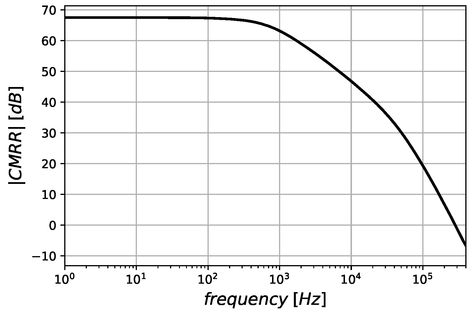
In this paper, we proposed an ultra-low-voltage amplifier that operates at a supply voltage of 0.3 V and attains good Figures of Merit for both small-signal and large-signal behaviors. The amplifier exploits a pseudo-differential body-driven fully differential input stage and a gate-driven second stage, which performs differential-to-single-ended conversion. This provides a rail-to-rail input common-mode signal swing, large DC gain and CMRR, and good frequency performance. In particular, the amplifier does not present high-impedance internal nodes thanks to the body-diode active loads; thus, it does not require Miller compensation. The gate terminals are used for biasing, thus achieving robustness against PVT variations.
The comparison against the state of the art of ULV OTAs has shown how the proposed topology optimizes the trade-off between small-signal and large-signal performance, and achieves very good values for all of the considered FOMs.
On the other hand, the proposed architecture presents limitations in terms of noise performance, exhibits an input impedance that is not purely capacitive, and shows a CMRR that is strongly dependent on mismatch variations. Another limitation is due to the body-driven current mirror load of the second stage, which causes an asymmetric slew rate. Nevertheless, these drawbacks are common to many ULV and ULP OTAs, in which a trade-off between many requirements has to be pursued.
It also has to be pointed out that, even if we presented results referring to a 130 nm CMOS process, the proposed topology can be implemented in even more advanced CMOS technology nodes, provided that the design guidelines outlined in the manuscript are properly followed. In particular, if a fully depleted silicon-on-insulator (FDSOI) CMOS process is available, the implementation of the proposed OTA (as well as of all body-driven OTAs) results in an input impedance similar to those of gate-driven circuits, and this is an interesting advantage over implementations based on conventional bulk CMOS processes, especially if switched applications are targeted.

Author Contributions

Conceptualization, R.D.S. and G.S.; methodology, F.C., R.D.S., P.M. and G.S.; software, R.D.S.; validation, F.C., R.D.S., P.M. and A.T.; formal analysis, F.C.; investigation, F.C., R.D.S. and G.S.; resources, A.T.; writing—original draft preparation, R.D.S.; writing—review and editing, F.C., P.M., G.S. and A.T.; supervision, G.S.; funding acquisition, A.T. All authors have read and agreed to the published version of the manuscript.

Funding

This research received no external funding.

Conflicts of Interest

The authors declare no conflict of interest.

Abbreviations

The following abbreviations are used in this manuscript:
BDBody-Driven
CMFBCommon-Mode Feedback
CMRRCommon-Mode Rejection Ratio
GDGate-Driven
FOMFigure of Merit
ICMRInput Common-Mode Range
IoTInternet of Things
OTAOperational Transconductance Amplifier
PSRRPower Supply Rejection Ratio
PTATProportional to Absolute Temperature
PVTProcess, Supply Voltage, and Temperature
THDTotal Harmonic Distortion
ULVUltra-Low Voltage
ULPUltra-Low Power

References

  1. Alioto, M. Enabling the Internet of Things—from Integrated Circuits to Integrated Systems; Springer: Berlin/Heidelberg, Germany, 2017. [Google Scholar]
  2. Toledo, P.; Rubino, R.; Musolino, F.; Crovetti, P. Re-Thinking Analog Integrated Circuits in Digital Terms: A New Design Concept for the IoT Era. IEEE Trans. Circuits Syst. II Express Briefs 2021, 68, 816–822. [Google Scholar]
  3. Aiello, O.; Crovetti, P.; Alioto, M. Ultra-Low Power and Minimal Design Effort Interfaces for the Internet of Things: Invited paper. In Proceedings of the 2019 IEEE International Circuits and Systems Symposium (ICSyS), Kuantan, Malaysia, 18–19 September 2019; pp. 1–4. [Google Scholar]
  4. Harpe, P.; Gao, H.; Dommele, R.V.; Cantatore, E.; van Roermund, A.H.M. A 0.20 mm2 3 nW Signal Acquisition IC for Miniature Sensor Nodes in 65 nm CMOS. IEEE J. Solid State Circuits 2016, 51, 240–248. [Google Scholar] [CrossRef] [Green Version]
  5. Avoli, M.; Centurelli, F.; Monsurrò, P.; Scotti, G.; Trifiletti, A. Low power DDA-based instrumentation amplifier for neural recording applications in 65 nm CMOS. AEU Int. J. Electron. Commun. 2018, 92, 30–35. [Google Scholar] [CrossRef]
  6. Lee, J.; Johnson, M.; Kipke, D. A Tunable Biquad Switched-Capacitor Amplifier-Filter for Neural Recording. Biomed. Circuits Syst. IEEE Trans. 2010, 4, 295–300. [Google Scholar] [CrossRef] [PubMed]
  7. Della Sala, R.; Monsurrò, P.; Scotti, G.; Trifiletti, A. Area-Efficient Low-Power Bandpass Gm-C Filter for Epileptic Seizure Detection in 130 nm CMOS. In Proceedings of the 2019 26th IEEE International Conference on Electronics, Circuits and Systems (ICECS), Genoa, Italy, 27–29 November 2019; pp. 298–301. [Google Scholar]
  8. Liu, Z.; Tan, Y.; Li, H.; Jiang, H.; Liu, J.; Liao, H. A 0.5-V 3.69-nW Complementary Source-Follower-C Based Low-Pass Filter for Wearable Biomedical Applications. IEEE Trans. Circuits Syst. I Regul. Pap. 2020, 67, 4370–4381. [Google Scholar] [CrossRef]
  9. Grasso, A.D.; Pennisi, S. Ultra-Low Power Amplifiers for IoT Nodes. In Proceedings of the 2018 25th IEEE International Conference on Electronics, Circuits and Systems (ICECS), Bordeaux, France, 9–12 December 2018; pp. 497–500. [Google Scholar]
  10. Stockstad, T.; Yoshizawa, H. A 0.9-V 0.5-/spl mu/A rail-to-rail CMOS operational amplifier. IEEE J. Solid State Circuits 2002, 37, 286–292. [Google Scholar] [CrossRef]
  11. Ferreira, L.H.C.; Pimenta, T.C.; Moreno, R.L. An Ultra-Low-Voltage Ultra-Low-Power CMOS Miller OTA With Rail-to-Rail Input/Output Swing. IEEE Trans. Circuits Syst. II Express Briefs 2007, 54, 843–847. [Google Scholar] [CrossRef]
  12. Yang, Y.; Li, Y.; Zhu, Z. A 0.8 V bulk-driven rail-to-rail operational amplifier. J. Circuits Syst. 2009, 29, 439–443. [Google Scholar]
  13. Raikos, G.; Vlassis, S. 0.8 V bulk-driven operational amplifier. Analog. Integr. Circuits Signal Process. 2010, 63, 425–432. [Google Scholar] [CrossRef]
  14. Pan, S.; Chuang, C.; Yang, C.; Lai, Y. A novel OTA with dual bulk-driven input stage. In Proceedings of the 2009 IEEE International Symposium on Circuits and Systems, Taiwan, China, 24–27 May 2009; pp. 2721–2724. [Google Scholar]
  15. Centurelli, F.; Monsurrò, P.; Parisi, G.; Tommasino, P.; Trifiletti, A. A Topology of Fully Differential Class-AB Symmetrical OTA With Improved CMRR. IEEE Trans. Circuits Syst. II Express Briefs 2018, 65, 1504–1508. [Google Scholar] [CrossRef]
  16. Ng, K.A.; Xu, Y.P. A Low-Power, High CMRR Neural Amplifier System Employing CMOS Inverter-Based OTAs With CMFB Through Supply Rails. IEEE J. Solid State Circuits 2016, 51, 724–737. [Google Scholar]
  17. Castaño, F.; Torelli, G.; Pérez-Aloe, R.; Carrillo, J.M. Low-voltage rail-to-rail bulk-driven CMFB network with improved gain and bandwidth. In Proceedings of the 2010 17th IEEE International Conference on Electronics, Circuits and Systems, Athens, Greece, 12–15 December 2010; pp. 207–210. [Google Scholar]
  18. Kumngern, M.; Khateb, F.; Kulej, T. 0.5 V bulk-driven CMOS fully differential current feedback operational amplifier. IET Circuits Devices Syst. 2019, 13, 314–320. [Google Scholar] [CrossRef]
  19. Centurelli, F.; Monsurrò, P.; Trifiletti, A. Comparative performance analysis and complementary triode based CMFB circuits for fully differential class AB symmetrical OTAs with low power consumption. Int. J. Circuit Theory Appl. 2016, 44, 1039–1054. [Google Scholar] [CrossRef]
  20. Grasso, A.D.; Marano, D.; Palumbo, G.; Pennisi, S. Design Methodology of Subthreshold Three-Stage CMOS OTAs Suitable for Ultra-Low-Power Low-Area and High Driving Capability. IEEE Trans. Circuits Syst. I Regul. Pap. 2015, 62, 1453–1462. [Google Scholar] [CrossRef]
  21. Zuo, L.; Islam, S.K. Low-Voltage Bulk-Driven Operational Amplifier With Improved Transconductance. IEEE Trans. Circuits Syst. I Regul. Pap. 2013, 60, 2084–2091. [Google Scholar] [CrossRef]
  22. Cabrera-Bernal, E.; Pennisi, S.; Grasso, A.D.; Torralba, A.; Carvajal, R.G. 0.7-V Three-Stage Class-AB CMOS Operational Transconductance Amplifier. IEEE Trans. Circuits Syst. I Regul. Pap. 2016, 63, 1807–1815. [Google Scholar] [CrossRef]
  23. Cellucci, D.; Centurelli, F.; Di Stefano, V.; Monsurrò, P.; Pennisi, S.; Scotti, G.; Trifiletti, A. 0.6-V CMOS cascode OTA with complementary gate-driven gain-boosting and forward body bias. Int. J. Circuit Theory Appl. 2020, 48, 15–27. [Google Scholar] [CrossRef]
  24. Khade, A.S.; Musale, S.; Suryawanshi, R.; Vyas, V. A DTMOS-based power efficient recycling folded cascode operational transconductance amplifier. Analog. Integr. Circuits Signal Process. 2021, 107, 227–238. [Google Scholar] [CrossRef]
  25. Manfredini, G.; Catania, A.; Benvenuti, L.; Cicalini, M.; Piotto, M.; Bruschi, P. Ultra-Low-Voltage Inverter-Based Amplifier with Novel Common-Mode Stabilization Loop. Electronics 2020, 9, 1019. [Google Scholar] [CrossRef]
  26. Baghtash, H.F. A 0.4 V, body-driven, fully differential, tail-less OTA based on current push-pull. Microelectron. J. 2020, 99, 104768. [Google Scholar] [CrossRef]
  27. Richelli, A.; Colalongo, L.; Kovacs-Vajna, Z.; Calvetti, G.; Ferrari, D.; Finanzini, M.; Pinetti, S.; Prevosti, E.; Savoldelli, J.; Scarlassara, S. A Survey of Low Voltage and Low Power Amplifier Topologies. J. Low Power Electron. Appl. 2018, 8, 22. [Google Scholar] [CrossRef] [Green Version]
  28. Centurelli, F.; Della Sala, R.; Scotti, G.; Trifiletti, A. A 0.3 V, Rail-to-Rail, Ultralow-Power, Non-Tailed, Body-Driven, Sub-Threshold Amplifier. Appl. Sci. 2021, 11, 2528. [Google Scholar] [CrossRef]
  29. Rodovalho, L.H.; Aiello, O.; Rodrigues, C.R. Ultra-Low-Voltage Inverter-Based Operational Transconductance Amplifiers with Voltage Gain Enhancement by Improved Composite Transistors. Electronics 2020, 9, 1410. [Google Scholar] [CrossRef]
  30. Veldandi, H.; Shaik, R.A. A 0.3-v pseudo-differential bulk-input ota for low-frequency applications. Circuits Syst. Signal Process. 2018, 37, 5199–5221. [Google Scholar] [CrossRef]
  31. Lv, L.; Zhou, X.; Qiao, Z.; Li, Q. Inverter-Based Subthreshold Amplifier Techniques and Their Application in 0.3-V ΣΔ-Modulator. IEEE J. -Solid-State Circuits 2019, 54, 1436–1445. [Google Scholar] [CrossRef]
  32. Colletta, G.D.; Ferreira, L.H.; Pimenta, T.C. A 0.25-V 22-nS symmetrical bulk-driven OTA for low-frequency G_m G m-C applications in 130-nm digital CMOS process. Analog. Integr. Circuits Signal Process. 2014, 81, 377–383. [Google Scholar] [CrossRef]
  33. Miguel, J.M.A.; Lopez-Martin, A.J.; Acosta, L.; Ramirez-Angulo, J.; Carvajal, R.G. Using Floating Gate and Quasi-Floating Gate Techniques for Rail-to-Rail Tunable CMOS Transconductor Design. IEEE Trans. Circuits Syst. I Regul. Pap. 2011, 58, 1604–1614. [Google Scholar] [CrossRef]
  34. Ferreira, L.; Sonkusale, S. A 60-dB gain OTA operating at 0.25-V power supply in 130-nm digital CMOS process. Circuits Syst. I Regul. Pap. IEEE Trans. 2014, 61, 1609–1617. [Google Scholar] [CrossRef]
  35. Kulej, T.; Khateb, F. A 0.3-V 98-dB Rail-to-Rail OTA in 0.18 μm CMOS. IEEE Access 2020, 8, 27459–27467. [Google Scholar] [CrossRef]
  36. Toledo, P.; Crovetti, P.; Aiello, O.; Alioto, M. Fully Digital Rail-to-Rail OTA With Sub-1000-μm2 Area, 250-mV Minimum Supply, and nW Power at 150-pF Load in 180 nm. IEEE Solid State Circuits Lett. 2020, 3, 474–477. [Google Scholar] [CrossRef]
  37. Toledo, P.; Crovetti, P.; Klimach, H.; Bampi, S. A 300 mV-Supply, 2 nW-Power, 80 pF-Load CMOS Digital-Based OTA for IoT Interfaces. In Proceedings of the 2019 26th IEEE International Conference on Electronics, Circuits and Systems (ICECS), Genoa, Italy, 27–29 November 2019; pp. 170–173. [Google Scholar]
  38. Kulej, T.; Khateb, F. Design and implementation of sub 0.5-V OTAs in 0.18-μm CMOS. Int. J. Circuit Theory Appl. 2018, 46, 1129–1143. [Google Scholar] [CrossRef]
  39. Kulej, T.; Khateb, F. A Compact 0.3-V Class AB Bulk-Driven OTA. IEEE Trans. Very Large Scale Integr. (VLSI) Syst. 2019, 28, 224–232. [Google Scholar] [CrossRef]
  40. Jérôme, F.K.; Evariste, W.T.; Bernard, E.Z.; Crespo, M.L.; Cicuttin, A.; Reaz, M.B.I.; Bhuiyan, M.A.S. An 8.72 µW Low-Noise and Wide Bandwidth FEE Design for High-Throughput Pixel-Strip (PS) Sensors. Sensors 2021, 21, 1760. [Google Scholar] [CrossRef]
  41. Mishra, R.B.; El-Atab, N.; Hussain, A.M.; Hussain, M.M. Recent Progress on Flexible Capacitive Pressure Sensors: From Design and Materials to Applications. Adv. Mater. Technol. 2021, 2001023. [Google Scholar] [CrossRef]
  42. Hajiaghajani, A.; Tseng, P. Microelectronics-Free, Augmented Telemetry from Body-Worn Passive Wireless Sensors. Adv. Mater. Technol. 2021, 2001127. [Google Scholar] [CrossRef]
  43. Gao, Y.; Soman, V.V.; Lombardi, J.P.; Rajbhandari, P.P.; Dhakal, T.P.; Wilson, D.G.; Poliks, M.D.; Ghose, K.; Turner, J.N.; Jin, Z. Heart Monitor Using Flexible Capacitive ECG Electrodes. IEEE Trans. Instrum. Meas. 2020, 69, 4314–4323. [Google Scholar] [CrossRef]
  44. Deo, N.; Sharan, T.; Dubey, T. Subthreshold biased enhanced bulk-driven double recycling current mirror OTA. Analog. Integr. Circuits Signal Process. 2020, 105, 229–242. [Google Scholar] [CrossRef]
  45. Abdelfattah, O.; Roberts, G.W.; Shih, I.; Shih, Y. An Ultra-Low-Voltage CMOS Process-Insensitive Self-Biased OTA with Rail-to-Rail Input Range. IEEE Trans. Circuits Syst. I Regul. Pap. 2015, 62, 2380–2390. [Google Scholar] [CrossRef]
  46. Magnelli, L.; Amoroso, F.A.; Crupi, F.; Cappuccino, G.; Iannaccone, G. Design of a 75-nW, 0.5-V subthreshold complementary metal–oxide–semiconductor operational amplifier. Int. J. Circuit Theory Appl. 2014, 42, 967–977. [Google Scholar] [CrossRef]
Figure 1. Block scheme of the proposed OTA.
Jlpea 11 00019 g001
Figure 2. Detailed schematic of the proposed OTA.
Jlpea 11 00019 g002
Figure 3. Differential gain of the proposed OTA: magnitude (a) and phase (b).
Jlpea 11 00019 g003
Figure 4. CMRR of the proposed OTA.
Jlpea 11 00019 g004
Figure 5. Schematic of the unity gain non-inverting buffer (a) and closed-loop frequency response (b).
Jlpea 11 00019 g005
Figure 6. DC input–output transfer characteristics of the buffer (a) and quiescent current of the input stage as a function of the input common-mode voltage (b).
Jlpea 11 00019 g006
Figure 7. Transient response to a full-swing square-wave input. (a) and the THD as a function of the peak-to-peak amplitude of the input voltage (b).
Jlpea 11 00019 g007
Figure 8. PSRR (a) and input-referred noise (b) of the proposed OTA.
Jlpea 11 00019 g008
Table 1. Transistor sizing and small-signal parameters of the proposed OTA.
W [ μ m]L [ μ m] I D [nA] g m [nS] g mb [nS] g ds [nS]
M 1 , 2 A ( B ) 15213396.365.382.13
M 3 , 4 A ( B ) 1.59.313335.458.614.13
M 5 , 6 129.3952462430.325.90
M 7 , 8 120295290335.2915.67
Table 2. Results of mismatched Monte Carlo simulations.
OutputOffset [mV]Pd [nW] SR p [V/ms] SR m [V/ms] SR AVG [V/ms]Gain (1 Hz) [dB]m φ [deg]GBW [kHz]CMRR [dB]
Mean0.07273.310.8232.3221.5742.9352.1218.651.77
Std Dev4.6147.1610.1890.4883.5973.1562.1875.64
Table 3. Amplifier performance vs. power supply voltage variations [±10%].
V d d - V s s [mV]270.0276.0282.0288.0294.0300.0306.0312.0318.0324.0330.0
Pd [nW]49.4153.4057.7762.5067.6073.0979.0085.3292.0499.11106.4
S R [ V m s ] 19.1021.4423.9026.5429.3732.3735.4838.6941.9245.1748.28
S R + [ V m s ] 9.40410.1310.7311.1111.1610.8310.219.4728.7278.0317.411
m φ [deg]71.3065.6461.0457.5754.6351.9349.3846.9944.8043.8642.32
DC Gain (dB)40.3239.8239.6139.8540.2940.8041.3641.9742.7143.6845.14
GBW [kHz]8.90810.7312.9615.0216.8718.6520.4122.1623.8225.2726.29
CMRR (dB)47.7551.1057.5865.0168.6767.4964.5461.4258.4655.7653.62
Offset [mV]3.8342.0491.0900.620.360.170.006−0.17−0.38−0.67−1.094
Noise [ μ V / H z ]2.3102.1842.1302.1202.1202.1232.1282.1332.1402.1512.172
Table 4. Amplifier performance vs. temperature variations: [−10, 110] °C.
Temperature [°C]−10.000.00010.0020.0030.0040.0050.0060.0070.0080.0090.00100.0110.0
Offset [mV]10.674.4591.3140.450.057−0.472−1.896−5.711−12.00−19.81−28.76−38.95−50.75
Pd [nW]36.9843.8853.0564.1777.1991.88106.7117.7123.8127.3130.0132.6136.2
DC Gain [dB]41.0343.1341.7140.9740.7640.9743.1457.9243.0035.3330.7527.2824.68
GBW [kHz]6.6408.19212.0416.1719.6522.4622.7620.6218.9317.5616.2214.8313.39
m φ 81.8474.8363.1355.8850.3846.0043.9845.8048.0249.3450.5151.9854.16
CMRR [dB]51.6851.0858.2370.9364.7555.8049.2858.5240.7931.4925.9922.2119.99
S R p [V/ms]10.5011.7812.2711.7810.328.5516.9965.8025.0014.5254.2113.9603.735
S R m [V/ms]22.6226.4129.0331.0832.9034.2735.1135.5535.6435.5035.1034.4633.54
S R A V G [V/ms]16.5619.1020.6521.4321.6121.4121.0520.6820.3220.0119.6619.2118.64
Noise [ μ V/ H z ]2.3672.1972.0422.0792.1432.2142.3482.7173.0953.3623.5633.7263.860
Table 5. Comparison with the state of the art.
This Work a [28] a [39] b [29] a [36] b [35] b [44] a [31] b [30] a [38] b [45] b [32] b [46] b [34] b
Year20212021202020202020202020202019201820182015201420142014
Technology [ μ m]0.130.130.181800.180.180.180.130.0650.180.0650.130.180.13
V D D [ V ] 0.30.30.30.30.30.30.50.30.30.30.350.250.50.25
V D D / V T H [ V ] 0.860.860.60.60.60.61.190.86-0.61.161.161.291.16
D C g a i n [dB]40.8064.664.7393098.169.549.86065.843-7060
C L [ p F ] 40503010150301525203203015
G B W [kHz]18.653.582.960.90.253.1369100702.783600-181.88
m φ [ d e g ] 51.9353.76529090546576536156-5552.5
S R + [ V m s ] 10.831.71.9-0.068149.7-256.445600-30.64
S R [ V m s ] 32.370.156.4-0.1014.29.7-257.85600-30.77
S R a v g [ V m s ] 21.600.934.15-0.0859.19.73.8257.12560094.6030.71
T H D [ % ] 1.40.841120.490.27--1-0.53-0.2
% of input swing8010085239083.3380--93.33-40-60
C M R R [dB]67.496111030416090-1267246---
P S R R [dB] c 4526/28D5633306181/99D-90/91D6235---
s p o t n o i s e [ μ V H z ] 2.122.691.60.81-1.80.910.0352.821.850.937.070.313.3
@freq1000100-1000--1000100,000100036-2001000100
P o w e r [nW]7311.412.60.62.4136018005115.417,000107518
M o d e BDBDBDGDDIGITALBDBDGDBDBDBDBDGDBD
I F O M S [ M H z · p F m A ] 3061471121144500468021484500303320581083223-3600392
I F O M L [ V · p F μ s · m A ] 305712242964-15906300121314007352790346-680146
F O M S [ M H z · p F m W ] 10,20015,702704715,00015,6007154900010,11168623610635-72001568
F O M L [ V · p F μ s · m W ] 11,82040799880-530021,0002425466624509247988-1200587
I F O M L W C [ V · p F μ s · m A ] 15891971357-127518901212-7352509345.8-600146
F O M L W C [ V · p F μ s · m W ] 59266584524-425063002425-24508364988-1200583
A r e a [mm 2 ]0.00360.00640.00850.000470.0009820.00980.0034-0.0030.00820.00500.0530.0570.083
a Simulated. b Measured. c P S R R + / P S R R [dB].
Publisher’s Note: MDPI stays neutral with regard to jurisdictional claims in published maps and institutional affiliations.

