
A New VCII Application: Sinusoidal Oscillators

 , , , ,
  ,
,  ,
,
Abstract
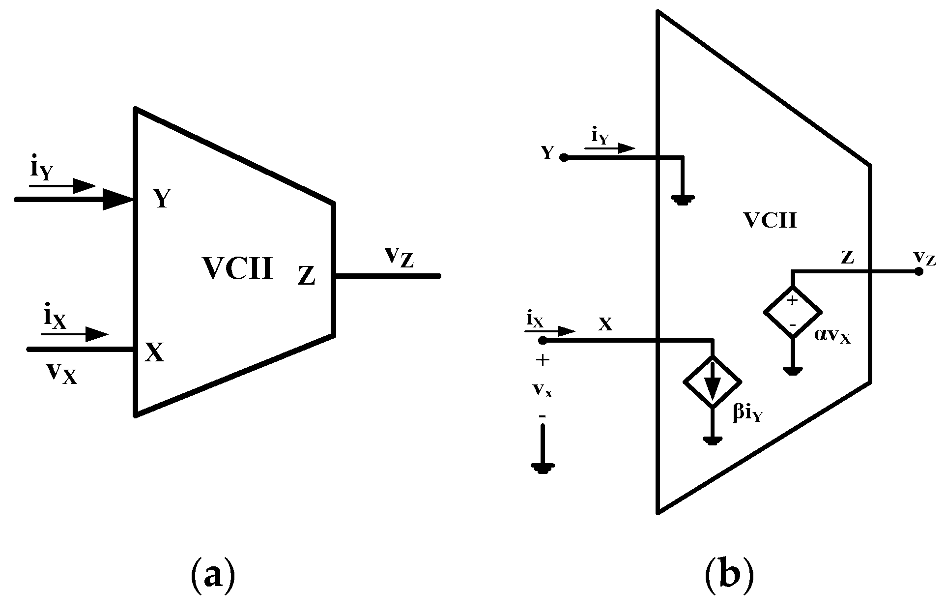
:1. Introduction
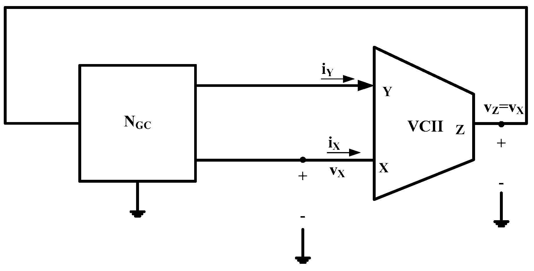
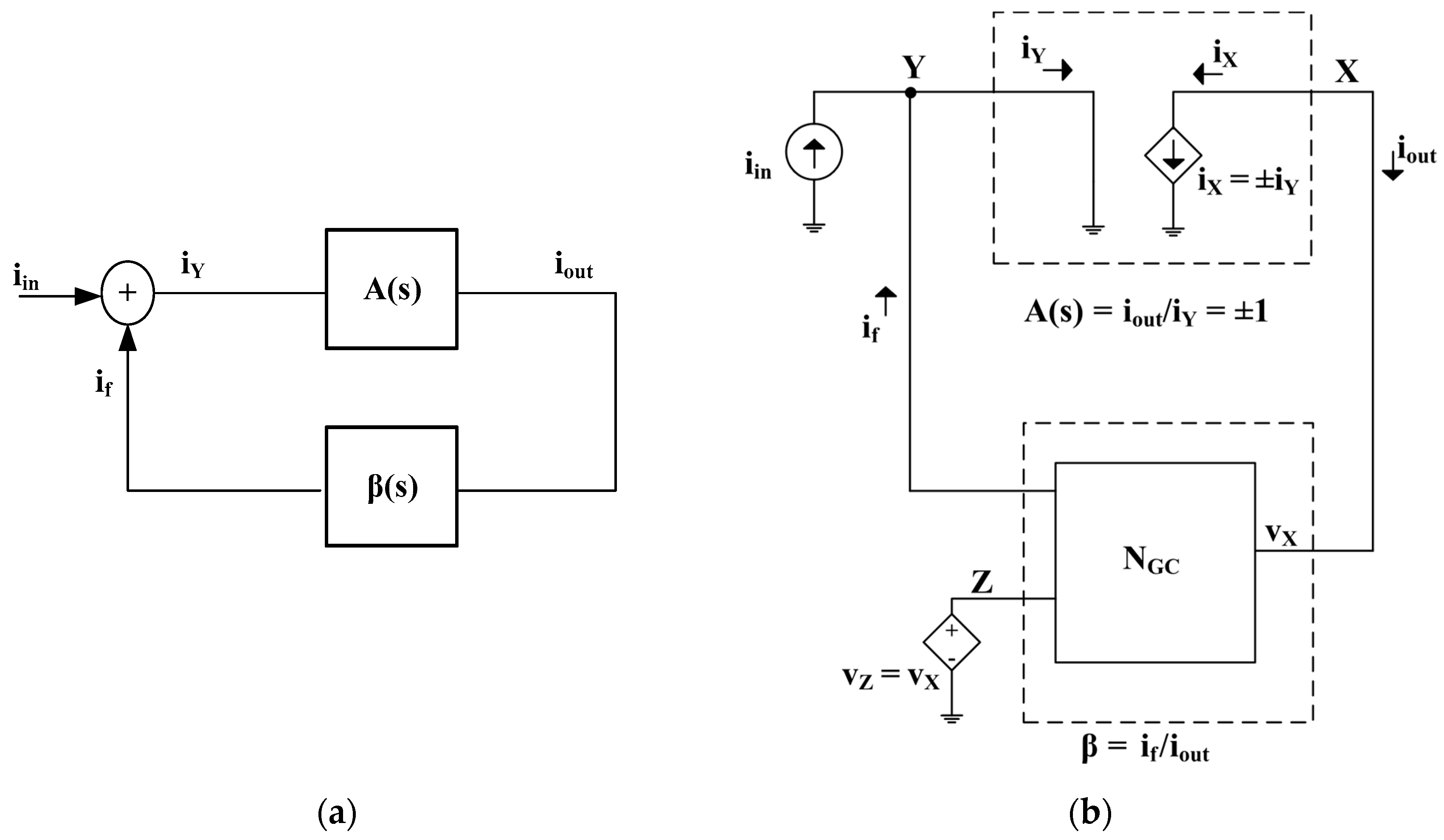
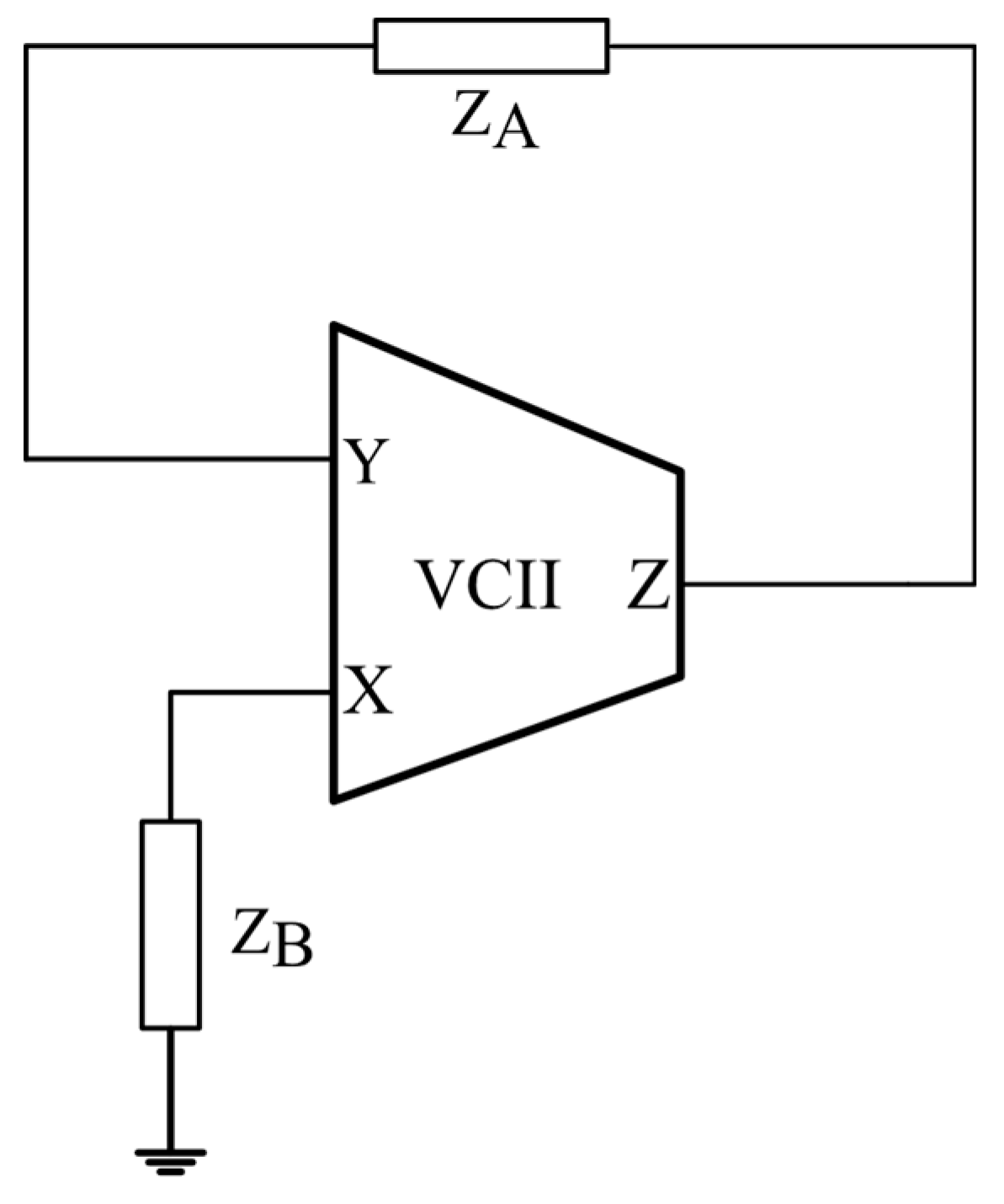
2. General Configuration of the VCII-Based Oscillator
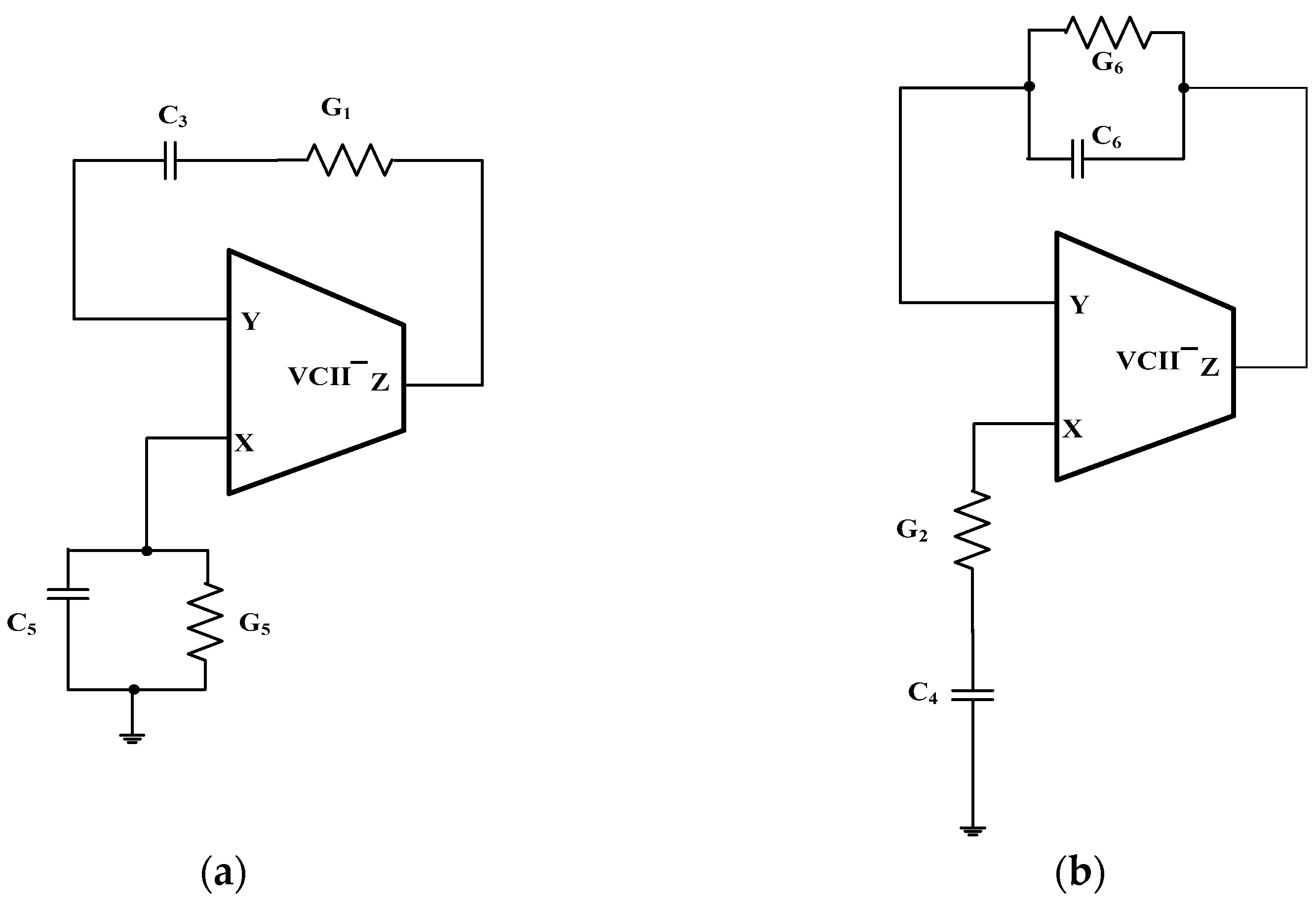
3. Oscillator Circuits
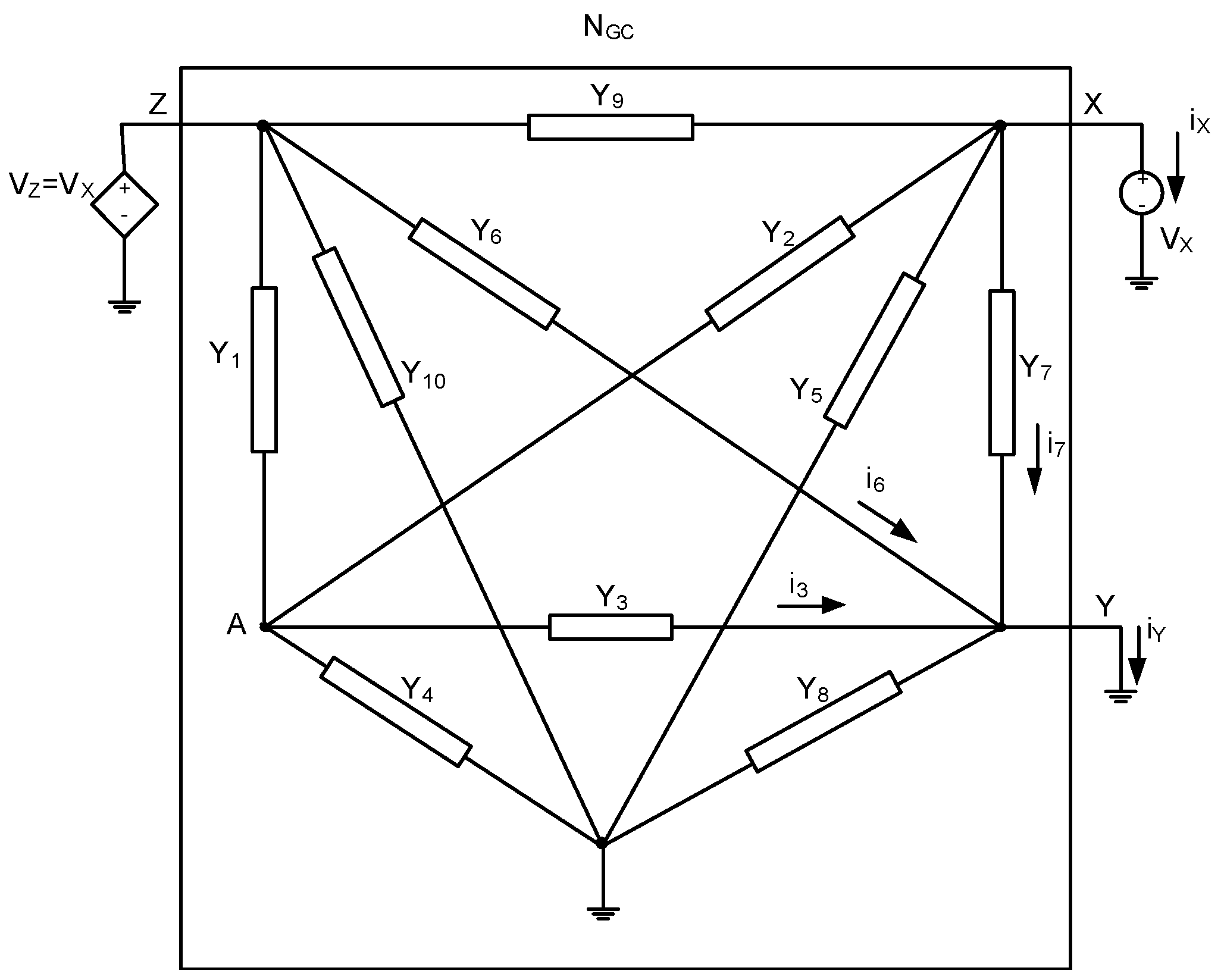
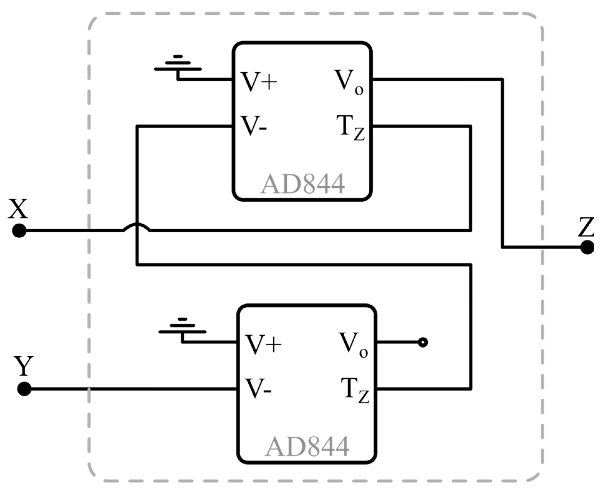
NGC as a Five-Node Network
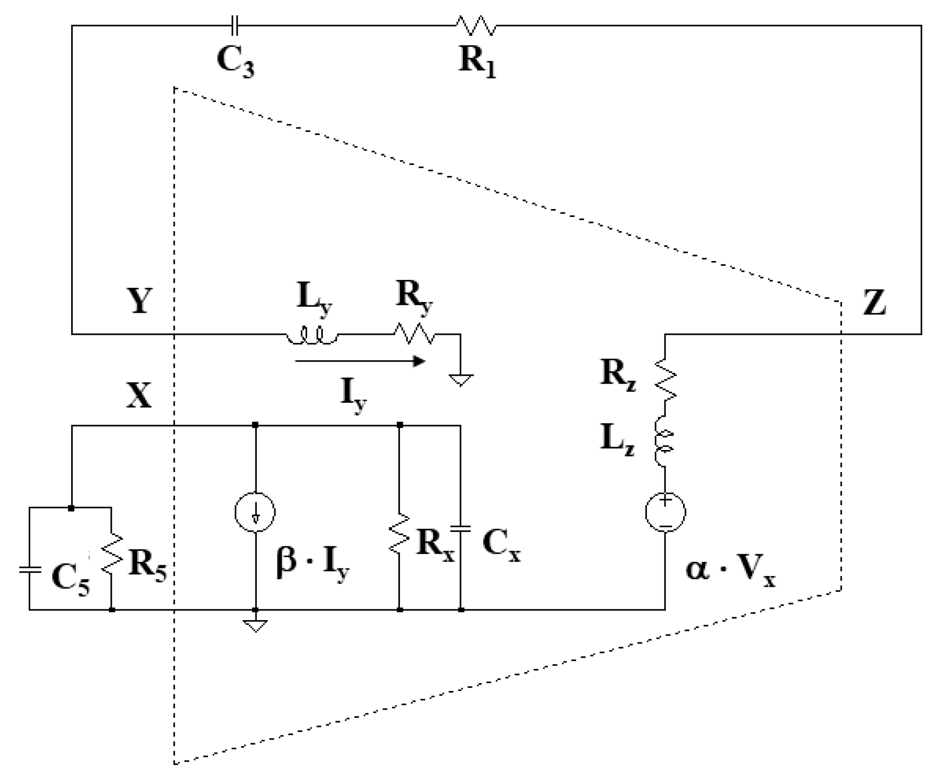
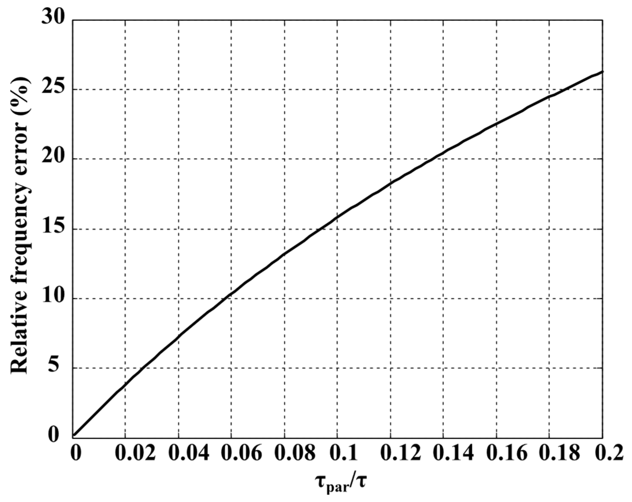
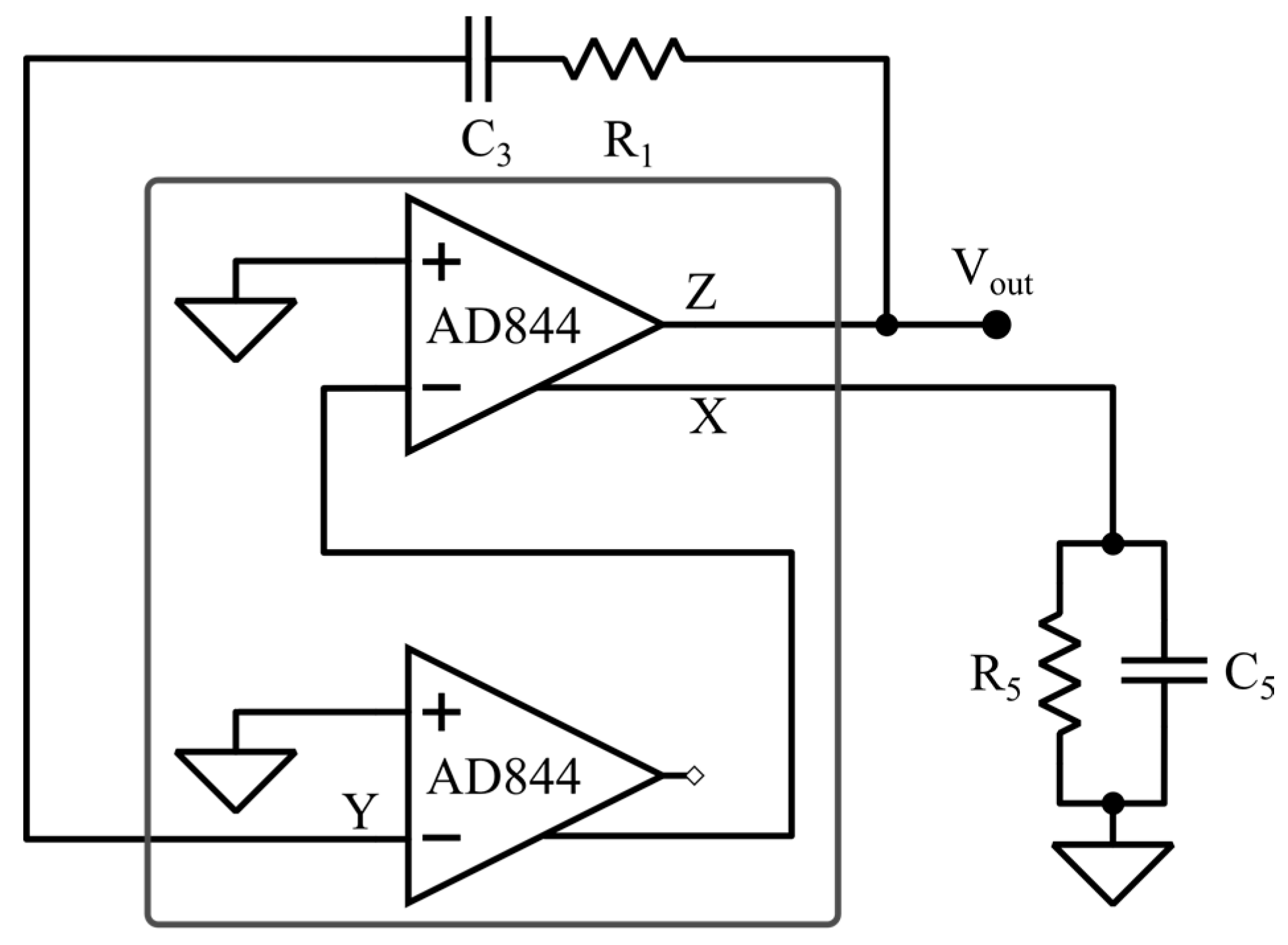
4. Analysis of Parasitic Effects: A Case Study
4.1. Resistive Port Impedances
4.2. Single-Pole Transfer Functions
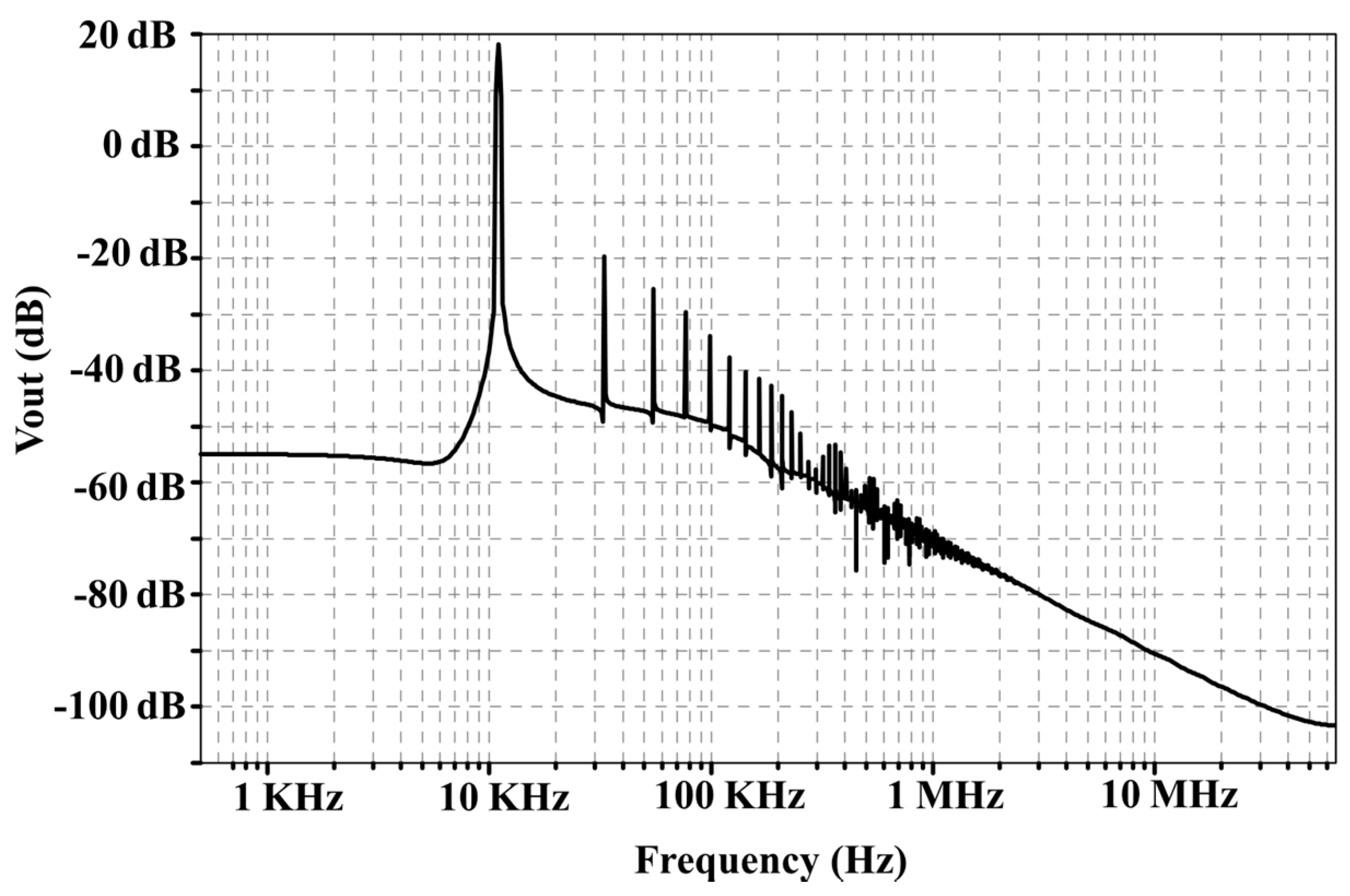
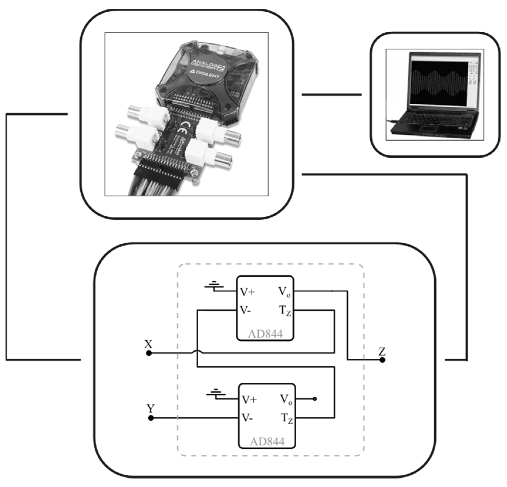
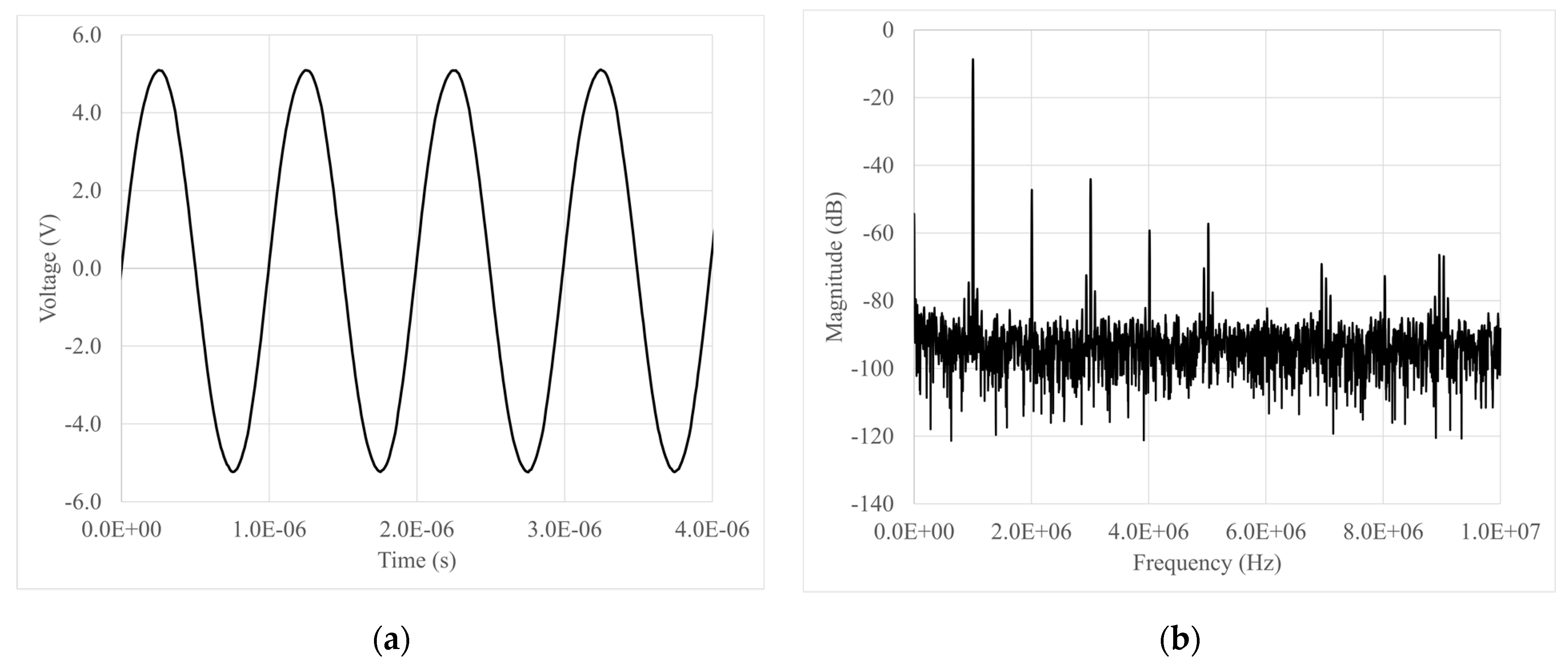
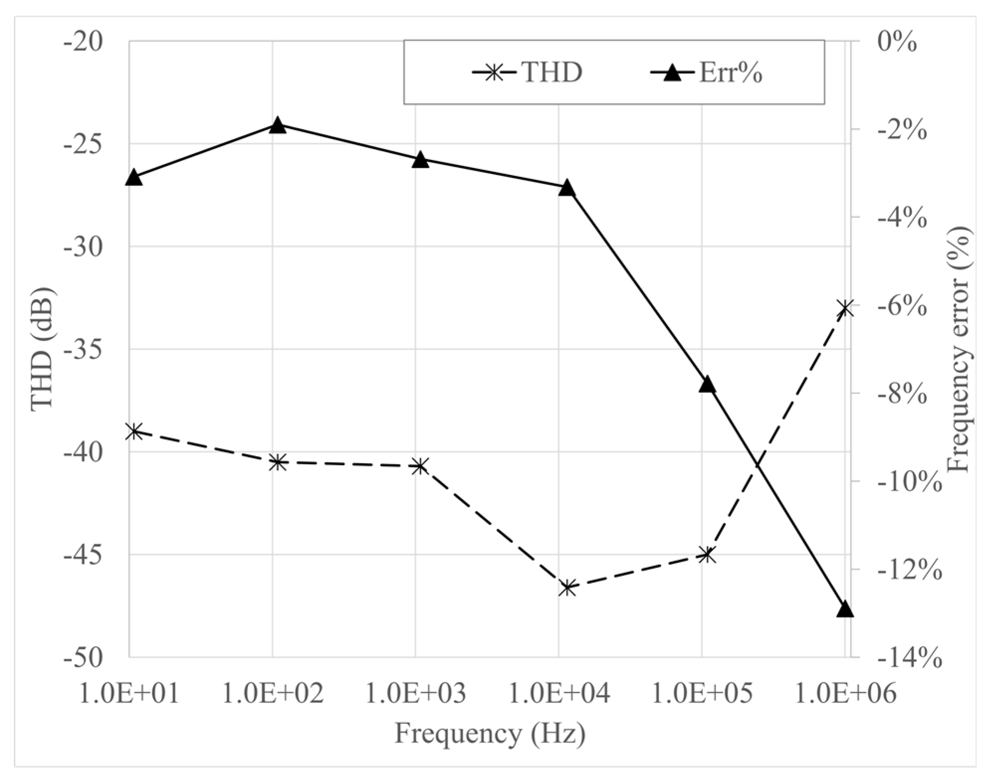
5. Experimental Results
6. Conclusions
Author Contributions
Funding
Data Availability Statement
Conflicts of Interest
References
- Jaikla, W.; Adhan, S.; Suwanjan, P.; Kumngern, M. Current/voltage controlled quadrature sinusoidal oscillators for phase sensitive detection using commercially available IC. Sensors 2020, 20, 1319. [Google Scholar] [CrossRef] [PubMed] [Green Version]
- Mohsen, M.; Said, L.; Elwakil, A.; Madian, A.; Radwan, A. Extracting optimized bio-impedance model parameters using different topologies of oscillators. IEEE Sensors J. 2020, 20, 9947–9954. [Google Scholar] [CrossRef]
- Li, G.; Cui, J.; Yang, H. A new detecting method for underwater acoustic weak signal based on differential double coupling oscillator. IEEE Access 2021, 9, 18842–18854. [Google Scholar] [CrossRef]
- Senani, R. New canonic sinusoidal oscillator with independent frequency control through a single grounded resistor. Proc. IEEE 1979, 67, 691–692. [Google Scholar] [CrossRef]
- Bhattacharyya, B.; Tavakoli Darkani, M. A unified approach to the realization of canonic RC-active, single as well as variable, frequency oscillators using operational amplifiers. J. Frankl. Inst. 1984, 317, 413–439. [Google Scholar] [CrossRef]
- Senani, R.; Bhaskar, D.R.; Gupta, M.; Singh, A.K. Canonic OTA-C sinusoidal oscillators: Generation of new grounded-capacitor versions. Am. J. Electr. Electron. Eng. 2015, 3, 137–146. [Google Scholar]
- Gupta, S.; Senani, R. State variable synthesis of single-resistance-controlled grounded capacitor oscillators using only two CFOAs: Additional new realisations. IEE Proc. Circuits Devices Syst. 1998, 145, 135–138. [Google Scholar] [CrossRef]
- Soliman, A.M. Current-mode oscillators using single output current conveyors. Microelectron. J. 1998, 29, 907–912. [Google Scholar] [CrossRef]
- Celma, S.; Martinez, P.A.; Carlosena, A. Approach to the synthesis of canonic RC-active oscillators using CCll. IEE Proc. Circuits Devices Syst. 1994, 141, 493–497. [Google Scholar] [CrossRef]
- Khan, A.A.; Bimal, S.; Dey, K.K.; Roy, S.S. Novel RC sinusoidal oscillator using second-generation current conveyor. IEEE Trans. Instrum. Meas. 2005, 54, 2402–2406. [Google Scholar] [CrossRef]
- Bajer, J.; Lahiri, A.; Biolek, D. Current-mode CCII+ based oscillator circuits using a conventional and a nodified Wien-bridge with all capacitors grounded. Radio Eng. 2011, 20, 245–251. [Google Scholar]
- Çam, U.G.; Toker, A.; Çicekoglu, O.G.; Kuntman, H. Current-mode high output impedance sinusoidal oscillator configuration employing single FTFN. Analog Integr. Circuits Signal Process. 2000, 24, 231–238. [Google Scholar] [CrossRef]
- Lahiri, A. New canonic active RC sinusoidal oscillator circuits using second-generation current conveyors with application as a wide frequency digitally controlled sinusoidal generator. Act. Passiv. Electron. Compon. 2011, 2011, 274394. [Google Scholar] [CrossRef]
- Horng, J.-W. Current-mode third-order quadrature oscillator using CDTAs. Act. Passiv. Electron. Compon. 2009, 2009, 789171. [Google Scholar] [CrossRef]
- Uttaphut, P.; Mekhum, W.; Jaikla, W. Current-mode multiphase sinusoidal oscillator using CCCCTAs and grounded elements. In Proceedings of the NEWCAS 11 IEEE 9th Int. New Circuits and Systems Conference, Bordeaux, France, 26–29 June 2011; pp. 345–349. [Google Scholar]
- Jin, J.; Wang, C. Current-mode universal filter and quadrature oscillator using CDTAs. Turk. J. Electr. Eng. Comput. Sci. 2014, 22, 276–286. [Google Scholar] [CrossRef] [Green Version]
- Agrawal, D.; Maheshwari, S. An active-C current-mode universal first order filter and oscillator. J. Circuits Systems Comput. 2019, 28, 1950219. [Google Scholar] [CrossRef]
- Soliman, A.M. Current-mode oscillators using inverting CCII. J. Act. Passive Electron. Devices 2011, 6, 305–320. [Google Scholar]
- Cam, U. A novel single-resistance-controlled sinusoidal oscillator employing single operational transresistance amplifier. Analog Integr. Circ. Sig. Proc. 2002, 32, 183–186. [Google Scholar] [CrossRef]
- Gupta, S.S.; Sharma, R.K.; Bhaskar, D.R.; Senani, R. Sinusoidal oscillators with explicit current output employing current-feedback op-amps. Int. J. Circuit Theory Appl. 2010, 38, 131–147. [Google Scholar] [CrossRef]
- Li, Y. Derivation for current-mode Wien oscillators using CCCCTAs. Analog Integr. Circ. Sig. Proc. 2015, 84, 479–490. [Google Scholar] [CrossRef]
- Abduelma’atti, M.T.; Alsuhaibani, E.S. New current-feedback operational-amplifier based sinusoidal oscillators with explicit current output. Analog Integr. Circ. Sig. Proc. 2015, 85, 513–523. [Google Scholar] [CrossRef]
- Sharma, R.K.; Arora, T.S.; Senani, R. On the realization of canonic single-resistance-controlled oscillators using third generation current conveyors. IET Circuits Devices Syst. 2017, 11, 10–20. [Google Scholar] [CrossRef]
- Chen, H.-P.; Hwang, Y.-S.; Ku, Y.-T. Voltage-mode and current-mode resistorless third-order quadrature oscillator. Appl. Sci. 2017, 7, 179. [Google Scholar] [CrossRef]
- Pushkar, K.L. Single-resistance controlled sinusoidal oscillator employing single universal voltage conveyor. SCIRP Circuits Syst. 2018, 9, 1–7. [Google Scholar] [CrossRef] [Green Version]
- Banerjee, K.; Singh, D.; Paul, S.K. Single VDTA based resistorless quadrature oscillator. Analog Integr. Circ. Sig. Proc. 2019, 100, 495–501. [Google Scholar] [CrossRef]
- Komanapalli, G.; Pandey, R.; Pandey, N. New sinusoidal oscillator configurations using operational transresistance amplifier. Int. J. Circuit Theory Appl. 2019, 47, 666–685. [Google Scholar] [CrossRef]
- Yuce, F.; Yuce, E. Supplementary CCII based second-order universal filter and quadrature oscillators. AEU Int. J. Electron. Commun. 2020, 118, 153138. [Google Scholar] [CrossRef]
- Srivastava, D.K.; Singh, V.K.; Senani, R. A class of single-CFOA-based sinusoidal oscillators. Am. J. Electr. Electron. Eng. 2020, 8, 1–10. [Google Scholar]
- Kumari, S.; Gupta, M. A new CMOS design of high transconductance current follower transconductance amplifier and its applications. Analog Integr. Circ. Sig. Process. 2018, 95, 325–349. [Google Scholar] [CrossRef]
- Pushkar, K.L.; Bhaskar, D.R. Voltage-mode third-order quadrature sinusoidal oscillator using VDIBAs. Analog Integr. Circ. Sig. Process. 2019, 98, 201–207. [Google Scholar] [CrossRef]
- Bhagat, R.; Bhaskar, D.R.; Kumar, P. Quadrature sinusoidal oscillators using CDBAs: New realizations. Circuits Systems Sig. Process. 2021, 40, 2634–2658. [Google Scholar] [CrossRef]
- Gupta, S.; Arora, T.S. Design and experimentation of VDTA based oscillators using commercially available integrated circuits. Analog Integr. Circ. Sig. Process. 2021, 106, 713–728. [Google Scholar] [CrossRef]
- Roy, S.; Pal, R.R. Electronically tunable third-order dual-mode quadrature sinusoidal oscillators employing VDCCs and all grounded components. Integr. VLSI J. 2021, 76, 99–112. [Google Scholar] [CrossRef]
- Safari, L.; Barile, G.; Stornelli, V.; Ferri, G. An overview on the second generation voltage conveyor: Features, design and applications. IEEE Trans. Circuits Syst. Part II Express Briefs 2019, 66, 547–551. [Google Scholar] [CrossRef]
- Safari, L.; Barile, G.; Ferri, G.; Stornelli, V. A new low-voltage low-power dual-mode VCII-based SIMO universal filter. Electronics 2019, 8, 765. [Google Scholar] [CrossRef] [Green Version]
- Safari, L.; Barile, G.; Ferri, G.; Stornelli, V. Traditional Op-Amp and new VCII: A comparison on analog circuits applications. AEU Int. J. Electron. Commun. 2019, 110, 152845. [Google Scholar] [CrossRef]
- Pantoli, L.; Barile, G.; Leoni, A.; Muttillo, M.; Stornelli, V. A novel electronic interface for micromachined Si-based photomultipliers. Micromachines 2018, 9, 507. [Google Scholar] [CrossRef] [PubMed] [Green Version]
- Barile, G.; Ferri, G.; Safari, L.; Stornelli, V. A new high drive class-AB FVF-based second generation voltage conveyor. IEEE Trans. Circuits Syst. Part II Express Briefs 2020, 67, 405–409. [Google Scholar] [CrossRef]
- Centurelli, F.; Monsurrò, P.; Tommasino, P.; Trifiletti, A. On the use of voltage conveyors for the synthesis of biquad filters and arbitrary networks. In Proceedings of the ECCTD 17 23rd Eur. Conf. Circuit Theory and Design, Catania, Italy, 4–6 September 2017. [Google Scholar]
- Yesil, A.; Minaei, S. New simple transistor realizations of second-generation voltage conveyor. Int. J. Circuit Theory Appl. 2020, 48, 2023–2038. [Google Scholar] [CrossRef]
- Al-Shahrani, S.M.; Al-Absi, M.A. Efficient inverse filter based on second-generation voltage conveyor (VCII). Arab J. Sci. Eng. 2021. [Google Scholar] [CrossRef]
- Al-Absi, M.A. Realization of inverse filters using second generation voltage conveyor (VCII). Analog Integr. Circ. Sig. Process. 2021. [Google Scholar] [CrossRef]
- Kumngern, M.; Torteanchai, U.; Khateb, F. CMOS class AB second generation voltage conveyor. In Proceedings of the 2019 IEEE International Circuits and Systems Symposium (ICSyS), Kuantan, Malaysia, 18–19 September 2019. [Google Scholar]
- Analog Devices. AD844 Datasheet and Product Info|Analog Devices. Analog.com. 2020. Available online: https://www.analog.com/en/products/ad844.html (accessed on 6 June 2021).
- Analog Discovery 2 [Digilent Documentation]. Available online: https://reference.digilentinc.com/reference/instrumentation/analog-discovery-2/start (accessed on 6 June 2021).
- Soliman, A.M. Current feedback operational amplifier based oscillators. Analog Integr. Circ. Sig. Process. 2000, 23, 45–55. [Google Scholar] [CrossRef]
- Chien, N.-C. New realizations of single OTRA-based sinusoidal oscillators. Act. Passiv. Electron. Compon. 2014, 2014, 938987. [Google Scholar] [CrossRef]
- Srivastava, D.K.; Singh, V.K.; Senani, R. Novel single-CFOA-based sinusoidal oscillator capable of absorbing all parasitic impedances. Am. J. Electr. Electron. Eng. 2015, 3, 71–74. [Google Scholar]
- Arora, T.S.; Gupta, S. A new voltage mode quadrature oscillator using grounded capacitors: An application of CDBA. Eng. Sci. Technol. 2018, 21, 43–49. [Google Scholar] [CrossRef]
- Komanapalli, G.; Pandey, N.; Pandey, R. New realization of third order sinusoidal oscillator using single OTRA. AEU Int. J. Electron. Commun. 2020, 93, 182–190. [Google Scholar] [CrossRef]


| C3 = 2C5 (nF) | R5 (kΩ) | R1 (kΩ) | f0 (Spice) (Hz) | f0 (Model) (Hz) | f0 Error (%) | THD (%) |
|---|---|---|---|---|---|---|
| 2000 | 15 | 7.3 | 10.8 | 10.74 | 0.6 | 0.7 |
| 200 | 15 | 7.35 | 107.3 | 107.0 | 0.3 | 0.4 |
| 20 | 15 | 7.35 | 1.073 K | 1.070 K | 0.3 | 0.4 |
| 2 | 15 | 7.3 | 10.80 K | 10.70 K | 0.9 | 0.5 |
| 0.2 | 15 | 6.9 | 108.1 K | 107.2 K | 0.9 | 0.7 |
| 0.2 | 1.5 | 0.65 | 1.080 M | 1.040 M | 3.7 | 1.7 |
| R1 (kΩ) | R5 (kΩ) | C3 (F) | C5 (F) | Ideal Frequency (Hz) | Measured Frequency (Hz) | Error (%) | THD (%) |
|---|---|---|---|---|---|---|---|
| 15 | 6.8 | 2 µ | 1 µ | 11.1 | 10.8 | −3 | 1.12 |
| 15 | 6.8 | 200 n | 100 n | 111 | 109 | −1.9 | 0.94 |
| 15 | 6.8 | 20 n | 10 n | 1.11 k | 1.08 k | −2.7 | 0.92 |
| 15 | 6 | 2 n | 1 n | 11.9 k | 11.5 k | −3.3 | 0.47 |
| 15 | 6 | 200 p | 100 p | 119 k | 109 k | −7.8 | 0.56 |
| 15 | 0.64 | 200 p | 100 p | 1.15 M | 1.0 M | −12.9 | 2.24 |
| Ref. | ABB Type | ABB Number | C (Grounded) | R (Grounded) | Output Phases | Indep. wo/Co |
|---|---|---|---|---|---|---|
| [5] | Op-Amp | 1 | 2 (2) | 4 (2) | 1 | NO |
| [7] | OTA | 3 | 2 (2) | -- | 2 | YES |
| [9] | CCII | 1 | 2 (2) | 2 (1) | 1 | NO |
| [9] | CCII | 1 | 2 (1) | 3 (3) | 1 | YES |
| [12] | FTFN | 1 | 2 (1) | 5 (1) | 1 | YES |
| [13] | CCII | 2 | 2 (2) | 2 (1) | 1 | YES |
| [16] | CDTA | 2 | 2 (1) | -- | 2 | NO |
| [19] | OTRA | 1 | 2 (0) | 3 (1) | 1 | YES |
| [21] | CCCCTA | 1 | 2 (2) | 1 (1) | 1 | YES |
| [23] | CCIII | 2 | 2 (2) | 3 (3) | 1 | YES |
| [25] | UVC | 1 | 2 (1) | 3 (1) | 1 | YES |
| [26] | VDTA | 1 | 2 (2) | -- | 2 | YES |
| [29] | CFOA | 1 | 3 (2) | 4 (2) | 1 | YES |
| [47] | CFOA | 1 | 2 (2) | 2 (1) | 1 | NO |
| [47] | CFOA | 1 | 2 (1) | 3 (1) | 1 | YES |
| [48] | OTRA | 1 | 2 (0) | 2 (0) | 1 | NO |
| [48] | OTRA | 1 | 2 (0) | 3 (1) | 1 | YES |
| [49] | CFOA | 1 | 3 (2) | 3 (3) | 1 | YES |
| [50] | CDBA | 2 | 2 (2) | 3 (0) | 2 | YES |
| [51] | OTRA | 1 | 3 (1) | 3 (0) | 1 | YES |
| This Work | VCII | 1 | 2 (1) | 2 (1) | 1 | NO |
Publisher’s Note: MDPI stays neutral with regard to jurisdictional claims in published maps and institutional affiliations. |
© 2021 by the authors. Licensee MDPI, Basel, Switzerland. This article is an open access article distributed under the terms and conditions of the Creative Commons Attribution (CC BY) license (https://creativecommons.org/licenses/by/4.0/).
Share and Cite
Stornelli, V.; Barile, G.; Pantoli, L.; Scarsella, M.; Ferri, G.; Centurelli, F.; Tommasino, P.; Trifiletti, A. A New VCII Application: Sinusoidal Oscillators. J. Low Power Electron. Appl. 2021, 11, 30. https://0-doi-org.brum.beds.ac.uk/10.3390/jlpea11030030
Stornelli V, Barile G, Pantoli L, Scarsella M, Ferri G, Centurelli F, Tommasino P, Trifiletti A. A New VCII Application: Sinusoidal Oscillators. Journal of Low Power Electronics and Applications. 2021; 11(3):30. https://0-doi-org.brum.beds.ac.uk/10.3390/jlpea11030030
Chicago/Turabian StyleStornelli, Vincenzo, Gianluca Barile, Leonardo Pantoli, Massimo Scarsella, Giuseppe Ferri, Francesco Centurelli, Pasquale Tommasino, and Alessandro Trifiletti. 2021. "A New VCII Application: Sinusoidal Oscillators" Journal of Low Power Electronics and Applications 11, no. 3: 30. https://0-doi-org.brum.beds.ac.uk/10.3390/jlpea11030030