
Comprehensive Study of Security and Privacy of Emerging Non-Volatile Memories


School of EECS, The Pennsylvania State University, State College, PA 16801, USA
*
Author to whom correspondence should be addressed.
J. Low Power Electron. Appl. 2021, 11(4), 36; https://0-doi-org.brum.beds.ac.uk/10.3390/jlpea11040036
Submission received: 25 July 2021
/
Revised: 23 August 2021
/
Accepted: 29 August 2021
/
Published: 24 September 2021
(This article belongs to the Special Issue Low-Power Hardware Security)
Abstract
:Several promising non-volatile memories (NVMs) such as magnetic RAM (MRAM), spin-transfer torque RAM (STTRAM), ferroelectric RAM (FeRAM), resistive RAM (RRAM), and phase-change memory (PCM) are being investigated to keep the static leakage within a tolerable limit. These new technologies offer high density and consume zero leakage power and can bridge the gap between processor and memory. The desirable properties of emerging NVMs make them suitable candidates for several applications including replacement of conventional memories. However, their unique characteristics introduce new data privacy and security issues. Some of them are already available in the market as discrete chips or a part of full system implementation. They are considered to become ubiquitous in future computing devices. Therefore, it is important to ensure their security/privacy issues. Note that these NVMs can be considered for cache, main memory, or storage application. They are also suitable to implement in-memory computation which increases system throughput and eliminates von Neumann bottleneck. Compute-capable NVMs impose new security and privacy challenges that are fundamentally different than their storage counterpart. This work identifies NVM vulnerabilities and attack vectors originating from the device level all the way to circuits and systems, considering both storage and compute applications. We also summarize the circuit/system-level countermeasures to make the NVMs robust against security and privacy issues.
1. Introduction
Static RAM (SRAM) [1,2,3,4,5,6,7,8,9,10] and dynamic RAM (DRAM) [11,12,13,14,15,16,17,18,19,20] (conventional volatile memories) suffer from significant leakage power and flash memory [21,22,23,24,25,26,27,28,29,30] (conventional non-volatile memories (NVMs)) suffers from high write power and poor endurance/performance. However, emerging NVMs can be beneficial since they offer zero leakage and high scalability, density, and endurance [31]. Some flavors of emerging NVMs are spin-transfer torque RAM (STTRAM) [32,33,34,35], magnetic RAM (MRAM) [36,37,38], phase-change memory (PCM) [39,40,41], resistive RAM (RRAM) [42,43,44], and ferroelectric RAM (FeRAM) [45,46]. Emerging NVMs can also bridge the widening performance gap between processor and memory. The majority of these memories are also compatible with conventional complementary metal oxide semiconductor (CMOS) technology, enabling easy integration with the logic process. Due to promising aspects, emerging NVMs are already being commercialized by industries, e.g., Everspin (MRAM) [47], Adesto (RRAM) [48], Intel/Micron (PCM) [49], and Cypress (FeRAM) [50]. Intel’s 3D Xpoint memory [49] is a recent example of NVM’s adoption as a cache for solid state drives. Applications of NVMs range from energy-harvested Internet-of-Things (IoT) and normally OFF devices such as body sensors and infrastructure health monitors [51] all the way to supercomputers. Significant effort has been devoted to integrating NVMs (henceforth, ‘NVM’ is used to denote ‘emerging NVM’) in different levels of memory hierarchy [32,33,34,35,36,37,38,39,40,41,42,43,44,45,46,51,52,53,54,55,56,57,58,59,60,61,62,63,64,65,66,67,68,69,70,71,72,73,74]. PCM and resistive RAM (RRAM) offer high TMR but are limited by their endurance/power requirement and are mainly considered for main-memory applications [39,40,44]. FeRAM is more suited towards main-memory applications due to a destructive read operation [46]. Spintronic memories such as STTRAM and MRAM offer very high endurance, high density, and low voltage operation, and are therefore more suitable for cache memory applications [32,33,34,37,38].
Prior research has shown significant energy and performance gain with NVMs [32,35,36,38,54,61,68,71,74]. They can provide desired memory bandwidth and reliability in high-performance computing, enable in-memory computing (IMC), an instant-ON feature and energy efficiency in mobiles, and power efficiency in IoTs. Although NVMs can reap energy and performance benefits, they may face new security issues that were not perceived before.
Motivational example: STTRAM contains a magnetic tunnel junction (MTJ) that acts as the storage component (Figure 1a). An MTJ contains one fixed and one free magnetic layer. The MTJ free layer’s magnetic orientation can be toggled from anti-parallel to parallel (or vice versa) by injecting current from bit-line to source-line (or vice versa). The security challenges of STTRAM pertain to persistent data and its sensitivity to ambient parameters that can be exploited for low-cost tampering. Similarly, RRAM is sensitive to temperature and gases which can be used to tamper with the data. Broadly, there are two major threats to NVMs’ security:
- (i)
- Threat to data security—pertains to data corruption (functional/timing) or destruction by a malicious attack to launch a denial-of-service (DoS) attack. The fixed layer of STTRAM is robust, however, the free layer could be toggled using both spin-polarized current and magnetic field [75]. Therefore, it is susceptible to manipulation through the magnitude and the polarity of the external magnetic field. Figure 1b,c show that the STTRAM free layer could flip its polarity either using current or with a 250 Oe magnetic field (easily produced by a horseshoe magnet). Figure 1d shows the number of errors in commercial MRAM using a permanent magnet [76]. Similar results can also be obtained through temperature modulation. Ensuring data security against malicious attacks through ambient effect is particularly critical in deployed systems where enforcing and maintaining physical security are difficult.
- (ii)
- Threat to data privacy—pertains to the compromise of sensitive data (e.g., keys, passwords, credit card details) present in raw form through unauthorized access and side channels. The desire to have a larger last level cache (LLC) for performance gain presents more persistent data that become vulnerable. The hard disk drive (HDD) has been the non-volatile part of the memory system. Encryption [77,78] is used to address the privacy of the sensitive data of the HDD. Volatile memory such as SRAM is considered safe due to the randomization of data at power down. As non-volatility is introduced at higher levels of memory stacks that were traditionally volatile, more data become vulnerable that were originally safe. As the memory level moves closer to the central processing unit (CPU), it becomes more sensitive to latency. Consequently, the application of encryption in LLC is difficult. Thus, addressing data privacy in higher levels of memory stack while maintaining performance is a challenge. New measures are required to resolve this. Designing a magnetic or heat shield around the device can be a possible solution but owing to its cost and weight, it may not be practical or effective for a range of applications including IoTs and mobiles. Existing packaging specification only considers the ambient stray magnetic field (~25 Oe). However, NVMs can face an intentional magnetic field and temperature which may not be protected by the packaging itself. Everspin lists the maximum magnetic tolerance for their MRAM chips during write/read/standby to be only ~100 Oe [47]. High and asymmetric write current [79] and long and asymmetric write latency [80] (common in most NVMs) can serve as side channels exposing the number of ‘1’s and ‘0’s in a memory word, weakening the data privacy [80,81,82,83,84]. Higher write current provides a knob to the adversary to launch fault injection [85], information leakage [86], and row hammer attack [87] through voltage droop/ground bounce. Furthermore, the inherent non-volatility of NVMs can be leveraged to design NVM Trojan [88,89] which is difficult to detect during the testing phase or prevent from being activated using system-level mitigation techniques.
Figure 1.
(a) Schematic of STTRAM; (b) flipping of MTJ free layer due to STT (Happ = 0 Oe, I = 0.638 mA) [90]; (c) flipping due to external magnetic field (Happ = 260 Oe, I = 0). Plots obtained using LLG equation with 60 × 120 × 3 nm MTJ, α = 0.01, Δ = 56, Ms = 1000 A/m, P = 0.8 [90]; (d) write errors with magnetic attack strength obtained from commercial MRAM chip.

Interestingly, the implementations and usages of NVMs for various applications such as cache, main memory, storage, and IMC vary significantly. Cache memory may employ IT-1S (S: storage), storage and main memory may use 1D-1S (D: diode), and IMC may use either of them but with different write/read/computing modes. Therefore, they may not be vulnerable to same attack models. Furthermore, if they suffer from the same vulnerability, a common solution may not be applicable to all application modes. For example, advanced wear-leveling techniques suitable for the main memory may not be applicable for cache as cache has tighter performance requirements. NVM Trojan triggers and payloads also differ with respect to NVM’s placement in the cache hierarchy. For example, a Trojan trigger inside the processor can directly tap the raw addressing of L1 cache for sensitization, however, a trigger in the main memory has to work harder to extract the trigger signal (naturally obfuscated due to address translation). Therefore, NVM vulnerabilities should be characterized for all application modes to get a deeper understanding. This will help to design and develop strong countermeasures.
This paper is related to [90] that reviews the security properties and applications of spintronic devices. The detailed differences are as follows: (i) We present security and privacy issues of a broad range of emerging non-volatile memories (NVMs) (such as STTRAM, RRAM, MRAM, PCM, and FeRAM) instead of focusing on only spintronic memories; (ii) we cover various vulnerabilities of various emerging NVMs such as supply noise and data signature leakage, etc. instead of vulnerabilities of spintronic memories such as susceptibility to external magnetic field and persistence; (iii) we cover a wide range of attack models such as side channel attack, fault injection attack, information leakage attack, row hammer attack and denial-of-service (DoS) attack instead of covering only external magnetic field and probing after power down; (iv) we present security issues of NVM as memory (for cache, main memory, and storage) as well as compute application.
The rest of the paper is organized as follows:
- Section 2 provides background on various NVM technologies and describes their vulnerabilities;
- Section 3 presents the privacy issues and countermeasures of NVM-based cache;
- Section 4 describes the NVM-enabled hardware Trojan attacks;
- Section 5 explains the security issues and countermeasures of NVM-based cache;
- Section 6 presents security and privacy analysis of NVM-based main memory and storage memory;
- Section 7 summarizes the threats to the compute-capable NVMs;
- Section 8 describes the test techniques to detect the security issues of NVMs after manufacturing;
- Section 9 presents the future directions for NVM security and privacy research;
- Finally, Section 10 draws the conclusion.
2. NVM Devices and Their Vulnerabilities
In this section, the basics of a few emerging NVM technologies are described along with their vulnerabilities. We mainly investigate STTRAM, MRAM, and RRAM for the sake of brevity and use them for drawing general conclusions on emerging NVMs. We also introduce other flavors of NVMs as necessary.
STTRAM/MRAM: STTRAM bitcell (Figure 2a) contains MTJ as the storage element which contains a free (FL) magnetic layer, a pinned (PL) (also known as fixed) magnetic layer, and an oxide layer between them. Each bitcell also contains an n-MOS as the selector device. Equivalent resistance of MTJ is high (denoted by RAP) if FL magnetic orientation is anti-parallel (AP) compared to the PL and the resistance is low (denoted by RP) if FL magnetic orientation is parallel (P) compared to the PL. MTJ can be toggled from P state (data ‘0’) to AP state (data ‘1’) (or vice versa) using current-induced spin-transfer torque by passing the appropriate write current (>critical current) from source-line (SL) to bit-line (BL) (or vice versa). MRAM bitcell (Figure 2b) is similar to STTRAM. However, the MRAM write operation is magnetic field driven. Current is passed through BL and digitline (DL) with appropriate direction and magnitude which flips the magnetic orientation of FL and thereby writes the data. During a read operation, a small voltage is applied and the resistance of the bitcell is sensed out for both STTRAM and MRAM.
Vulnerabilities: STTRAM/MRAM suffers from:
- (i)
- (ii)
- (iii)
- Susceptibility to external fields: An external magnetic field can lead to magnetic orientation flip of MTJ free layer of MTJ which corrupts the data [80]. Adversary can leverage this to launch attacks (e.g., DoS).
- (iv)
- Susceptibility to temperature: High temperature reduces data retention. An adversary can trigger a DoS attack by leveraging this.
RRAM: RRAM contains an oxide material between two electrodes. The electrodes are known as bottom electrode (BE) and top electrode (TE) (Figure 3). A conduction filament (CF) can be created or broken by oxide break down and re-oxidation. These can be done by applying an electric field (by applying a voltage across RRAM). The two resistance states of the RRAM are termed as high resistance state (HRS) and low resistance state (LRS). LRS → HRS switching is known as SET and HRS → LRS switching is known as RESET. During a read operation, a small voltage is applied and the resistance of the bitcell is sensed out.
Vulnerabilities: RRAM suffers from (i) asymmetric write and read current; (ii) high write current; (iii) susceptibility to external temperature; and (iv) low endurance. The adversary could hammer a memory bitcell to exhaust the lifetime of RRAM.
PCM: There are two major PCM designs: Heater based (Figure 4a) and self-heating based (Figure 4b) [91]. The first one contains a material layer (e.g., titanium nitride or tungsten [91,92,93]) that acts as a heat source to heat the adjacent layer of phase-change material [91]. The latter relies on the internal generated heat within the PCM and helps the state change of the material. Ge2Sb2Te5 (GST) [92,94] is used as a phase-change material for both designs. Another example of a similar phase-change material is In3Sb1Te2 [95,96,97].
A current is applied through the PCM cell to force the cell to either SET (low resistance) or RESET (high resistance) during write. A small voltage is applied across the cell during read operation and the resistance is sensed to read the stored data. Vulnerabilities PCM suffers from include (i) asymmetric write/read current; (ii) high write current; and (iii) low endurance. The adversary can hammer a cell to exhaust the lifetime of the PCM. The adversary could hammer a memory bitcell to exhaust the lifetime of RRAM.
FeRAM: FeRAM bitcell (Figure 5) contains one capacitor and one access transistor. The bitcell is similar to DRAM, except a dielectric structure containing ferroelectric material is used in FeRAM instead of a linear capacitor. During a write operation, an applied electric field across the ferroelectric layer is applied which forces the atoms inside into the ‘up’ or ‘down’ orientation (based on electric field polarity), thereby storing a ‘1’ or ‘0’. During a read operation, the transistor forces the cell into a particular state, say ‘0’. If the cell is holding a ‘0’, bit-line voltage remains the same. Otherwise, the re-orientation of the atoms in the film will cause a brief pulse of current in the output which indicates the cell is held a ‘1’. Note that FeRAM read is destructive in nature and requires the cell to be re-written.
Vulnerabilities: FeRAM suffers from (i) asymmetric read current; (ii) high write current; and (iii) susceptibility to an external thermal and electric field. An adversary can launch a DoS attack by applying an external electric field.
Comparative Analysis
Table 1 summarizes the vulnerabilities of some of the emerging NVMs along with conventional memories. The vulnerabilities can be categorized into data privacy and data security. Side channel, fault injection, information leakage, and row hammer attacks can be termed as data privacy attacks whereas DoS, thermal, magnetic, and electric field attacks can be termed as data security attacks. From the table, it can be noted that spintronic memories are more vulnerable to the attacks while FeRAM is the least. Additionally, SRAM is susceptible to side channel attack and DRAM is susceptible to row hammer attack [99,100,101,102,103,104,105,106,107,108]. In the following sections, the data security and privacy attacks on NVMs are explained.
3. Privacy Issues and Countermeasures of NVM-Based Cache
In this section, the privacy issues related to the NVM-based cache and various countermeasures are explained.
3.1. Side Channel Attack (SCA)
In this subsection, NVM susceptibility to SCA is discussed, taking STTRAM as a test case. However, other NVMs also exhibit similar susceptibility.
3.1.1. Background
SCA [109] targets the weak implementation of cryptographic algorithms. The weakness in the implementation may arise from several factors such as the design of the compute element or its device physics. This makes it difficult to fix the issue.
SCA exploits the various leakages observed in various physical channels, such as timing [110], consumption of power [109], emanation of electromagnet (EM) [111], etc., to extract the secret key. Compared to conventional SCA that exploits the computing elements such as SBOX to extract information, SCA on memory is based on the observation of physical signature during the read/write of sensitive data. A physical signature which is dependent on the value of a secret key can in turn reveal the secret since (0 → 1/1 → 0) data transitions have different and distinctive physical signatures (e.g., read/write time, consumption of power or current, etc.). SCA targets a sensitive computation device that reveals a physical signature dependent on the key value leveraging assumptions on the leakage model.
The Hamming distance (HD) model is used for memory SCA. The HD is equal to the number of bit transitions taking place while the value in the memory bitcell is being updated. Next, a statistical dependency between the observed leakage and the hypothetical leakage (computed leveraging some hypotheses and the leakage model) is tested.
One major advantage of SCA is that it can leverage the divide and conquer approach. Basically, SCA can recover small key parts independently at once and later they can be combined to get the full key. This enables the attacker to exhaustively test all hypotheses on the keys. For example, a 128-bit AES key has 2128 possible combinations and it is practically impossible to test all of them. Instead, if SCA targets 8 bits of the key at a time, the key hypothesis reduces to 28. The rest of the 120 bits is considered as noise. The correct key hypothesis exhibits a significantly higher statistical dependency compared to others if the attack is successful. Once the first 8 bits of the key are recovered, the attack can be repeated 16 more times to retrieve the rest of the key. This reduces the complexity to 28 × 16 = 212 from 2128. Difference of means (DoM) [111] and the Pearson correlation coefficient [112] are some widely used statistical tools.
3.1.2. SCA on STTRAM
STTRAM write current is a function of the polarity of the stored data. The equivalent resistance of MTJ is low (high) in state ‘0’ (‘1’). Figure 6a shows Iwrite for 1 → 0. During write, the initial current is high since MTJ resistance is low. However, the current becomes low after successful write. Similarly, write current for 1 → 0 goes from low to high (Figure 6b).
Note that three phases can be identified in the waveform for Iwrite of 0 → 1 and 1 → 0; ‘old data’, ‘transition from old data to new data’, and finally, ‘new data’. Iwrite of 1 → 1 and 0 → 0 are fairly constant since the MTJ state does not change. The current magnitude difference of low and high states of current waveform (for 0 → 1 and 1 → 0) is significant and, therefore, reveals the information about new and previous data.
The read current for both data ‘0’ and ‘1’ (Figure 6c) depends on the current state of the bit. Therefore, the key could be extracted when it is being read during the intermediate steps of an encryption operation (such as AES or MICKEY-128 2.0). Furthermore, read/write operations can be distinctly identified from the corresponding current waveforms.
In [84], a differential power analysis (DPA) on STTRAM read/write operation and MRAM read operation is performed. The work used the HD model with Pearson correlation. The key extraction is focused during the AES-128 last round. The first byte of the key can be retrieved in around 600 traces, which is suboptimal. The work further improved the attack model with some basic pre-processing (subtracting the average initial write current from the final write current, which results in the change in write current). The result is shown in Figure 7a. The black line is the correct hypothesis and the attack is considered successful when it emerges from the cloud of all wrong hypotheses. Similarly, analysis is extended to STTRAM read operation and SRAM write operation. Figure 7b summarizes the result. STTRAM write operation revealed 8 bytes of the key in ~2000 traces before the pre-processing. However, after pre-processing, STTRAM write reveals all 16 bytes in ~1600 traces. Note that the latter is similar to SRAM write operation. However, STTRAM read is more vulnerable as it leaks the full key (16bytes) in only ~400 traces.
The work further verified the analysis on MRAM read operation using a commercial MRAM chip. A window of 15 ns (termed as window of interest (WOI)) is identified that relates to the sensing of data from bitcells. Figure 8 shows the average read current in the WOI for data 0 to 255. It is apparent that the read current is a function of the number of ones in 8-bit data. A trend can be observed where read current reduces as Hamming weight (HW) increases. This proves that MRAM read current reveals the stored data. The work further shows that the attack on MRAM read can retrieve the key (Figure 9).
In [83], a correlation power analysis (CPA) on MRAM write operation was performed. The work proposes a hypothetical power model that considers the difference of 0 → 1 and 1 → 0 transitions to estimate the post-alignment power consumption while writing to MRAM. They considered the stream cipher MICKEY-128 2.0 to validate the proposed attack model. The results show that the secret key can be retrieved from MRAM write operation traces.
3.1.3. Considerations for Other NVMs
SCA exploits asymmetric write current to extract data. Since all NVMs (except technologies such as spin-orbit torque MRAM) incur asymmetric write and/or read current, they are equally susceptible to SCA.
3.1.4. Countermeasures
The asymmetry (data dependent) in the Iread/Iwrite current needs to be eliminated to secure the memory against SCA. Data encoding could be one solution [84]. However, note that it can be very sensitive to process variation [113]. A solution to remove write asymmetry could be to implement constant current write [84]. However, this method incurs high power overhead. Another method to eliminate side channels is to mask the asymmetry using an on-chip capacitor [114] and stable voltage regulators [115,116].
3.2. Fault Injection Attack
In this subsection, NVM susceptibility to fault injection attack is discussed, taking RRAM as a test case. However, other NVMs also exhibit similar susceptibility.
3.2.1. Background
Fault injection attacks during write (read) operation can prevent successful writing of specific data polarity (read incorrect data for specific data polarity). Such attacks can be exploited to leak system assets such as cryptographic keys. One example is when an adversary induces multi-bit or single-bit faults in a system (cryptographic) and performs differential analysis to extract the keys. The differential analysis could be done by observing correct and faulty pairs of input/output and in turn deriving simplified equations. Several studies have shown techniques to extract sensitive keys by injecting faults [117]. In contrast to existing methods that focus on fault injection in clock and/or power rail, we describe techniques that inject faults in NVMs.
In [85], a fault injection attack on NVM (taking RRAM as a test case) using supply noise was investigated. Figure 10 shows a high-level idea. An adversary writes in their memory space and generates a specific supply noise which can propagate to a victim’s memory space and cause failures in a specific polarity read/write operation.
3.2.2. Attack Model and Assumption
It has been shown [85] that an adversary can leverage high/asymmetric write current and long latency of NVMs (which causes supply voltage droop and ground bounce) to launch fault injection attacks. An adversary can write specific data patterns (i.e., a specific number of 0s and 1s) to generate deterministic droop/bounce. This will propagate to the user’s memory space and create read/write failure. For this analysis, an RRAM-based (i.e., 1T1R) last level cache (LLC) has been considered as a test case.
The work [85] assumes that: (i) NVM LLC is being shared by two users (i.e., an adversary and a victim); (ii) bank-level parallel read/write operation is performed to increase the throughput; (iii) the adversary has the knowledge of the amount of droop/bounce that can be generated by a read/write data pattern; (iv) the adversary also knows how the generated droop/bounce propagates (decays with distance) and how it affects the victim’s write/read operation; (v) the adversary is an expert in computer architecture and can exploit knobs, e.g., accessing specific data patterns in pre-defined physical locations to prevent their replacement by policies, e.g., least recently used (LRU).
3.2.3. Supply Noise Due to High Write Current
High current (50–100 mA assuming ~100 μA/bit) is drawn from the supply for a full cache line (512–1024 bit) write. This creates two types of supply noise:
- Supply voltage droop: On-chip voltage regulator or power supply keeps the supply voltage constant. However, the supply voltage (distributed in metal M8) reaches the memory bitcell (implemented in metal M1) via the power-grid RC network. The interconnect resistance causes a significant voltage droop at the bitcell due to high current. Voltage droop lowers headroom for the bitcell and increases the write latency or decreases the sense margin for the read. It can eventually lead to a read/write failure.
- Local ground bounce: Similar to supply voltage, the true ground is routed on the upper metal layer (e.g., M8) and connects to the transistors in M1. Therefore, the local ground rail bounces when the charge (due to high write/read current) is dumped.
Droop/bounce magnitude depends on the present state of the memory bit as well as the new data being written since Iwrite for 0 → 0, 0 → 1, 1 → 0 and 1 → 1 is different (for a write operation), and on the stored data (for a read operation). For example, Figure 11a shows the bounce generated by a full cache line write for various data patterns. It is notable that 1 → 1 write creates the lowest and 0 → 0 creates the highest bounce.
3.2.4. Fault Injection Using Write Operation
RRAM write with additional supply noise (generated from another parallel operation) is simulated generated by a parallel operation [86]. As supply noise increases, write latency for both LRS to HRS and HRS to LRS increases. Figure 11b shows the RRAM resistance switching during write operation with respect to supply noise. Supply noise beyond 50 mV and less than 120 mV will cause LRS to HRS write failure but successful HRS to LRS write is still possible. If the adversary can generate supply noise in a way that the victim incurs noise in this range, it will launch a 0 → 1 polarity fault injection attack. However, if the victim incurs combined voltage loss > 120 mV, it will cause complete write failure, i.e., DoS attack.
Detection of victim’s write initiation: The adversary needs to know when and where the user is writing to launch DoS/fault injection/information leakage attack (discussed in the next subsection). One possible approach adopted by the adversary is to store data that generates high noise (i.e., all 0) in various locations of the memory and read them frequently. If a read error occurs, it can be assumed that the victim has started a write operation nearby. This is true since the victim’s read cannot generate enough noise to cause failure in the adversary’s read operation.
3.2.5. Fault Injection Using Read Operation
Figure 12a shows the supply noise generated by various read data patterns. It can be noted that the adversary can control generated noise magnitude by reading specific data patterns (stored before launching an attack). Figure 12b shows that the sense margin reduces with supply noise. However, ground bounce causes a greater effect compared to droop as it (i) reduces the discharge current and (ii) reduces VGS of the access transistor (RTransistor is higher) while voltage droop only reduces the discharge current. It is evident from Figure 12b that if the adversary can generate supply noise in a way that the victim incurs noise > 150 mV, the victim will read ‘1’ incorrectly. However, injecting a read error into data ‘0’ requires significantly higher noise. Therefore, both polarity read failures (DoS by a read failure) might not be possible as the required noise is too high.
3.2.6. Considerations for Other NVMS
The NVM fault injection attack leverages supply noise. Since all NVMs incur high supply noise due to their high write current and their write current/time for data ‘0’ and data ‘1’ are asymmetric, all NVMs are susceptible to a similar fault injection attack.
3.2.7. Countermeasures
Following techniques can prevent or alleviate the attack:
- (i)
- Sequential read/write access: This can be a naïve solution as non-pipelined access hurts system throughput. However, the adversary will not be able to create droop/bounce or sense data by launching parallel access.
- (ii)
- Architecture-level mitigation: Parallel operations of different processes can be initiated to addresses with highest possible RInt. This will alleviate the issue to some extent.
- (iii)
- Good quality power/ground grid: A good power/gnd grid reduces supply line parasitics which in turn reduces bounce. However, this cannot eliminate the issue.
- (iv)
- Power rail separation for each bank: Separation of supply and gnd rails between parallel accessed banks will prevent the propagation of supply noise. However, this will incur significant area-overheard and reduce the power rail capacitance (which is not desirable).
- (v)
- System clock slow down: Higher TClock gives more time to read/write at lower headroom voltage to fix latency failures.
3.3. Information Leakage Attack
In this section, we describe an information leakage attack to approximate the HW of the victim’s data by an aggressor in a shared computing environment. RRAM is taken as a test case.
3.3.1. Overview of Information Leakage Attack by Supply Noise
Figure 13 shows the concept of an information leakage attack by leveraging supply noise. The victim writes sensitive data patterns which create data-dependent supply noise and propagate to the adversary memory space. The adversary reads known data (i.e., known supply noise) which adds up to the propagated noise and creates a read failure. From the read failure, the adversary can detect the amount of sensitive noise from the victim and back-calculate the HW of the victim’s sensitive data. For example, if the victim writes data that generates > 150 mV droop in the adversary’s memory space, the adversary can conclude that the victim’s write data HW is >66.77% (with some assumptions).
3.3.2. Attack Model and Assumption
It has been shown that an adversary can leverage a high and asymmetric write current and long latency of NVMs (which causes supply voltage droop and ground bounce) to approximate the HW of the victim’s write data [86]. An adversary can keep reading data in their memory space. If a read failure is incurred, the adversary can approximate the noise generated by the victim’s write data which can further reveal the range of the HW of the data. For this analysis, an RRAM-based (i.e., 1T1R) last level cache (LLC) has been considered as a test case.
It has been assumed [86] that: (i) NVM LLC is being shared by two users (i.e., an adversary and a victim); (ii) a bank-level parallel read/write operation is performed to increase the throughput; (iii) the adversary has the knowledge of the amount of droop/bounce that can be generated by a read/write data pattern; (iv) the adversary also knows how the generated droop/bounce propagates (decays with distance) and how it affects the victim’s write/read operation; (v) the adversary is an expert in computer architecture and can exploit knobs, e.g., accessing specific data patterns in pre-defined physical locations to prevent their replacement by policies, e.g., least recently used (LRU).
3.3.3. Data Information Approximation
RRAM write waveforms can be divided into two regions with respect to time. The first region represents the old data state and the last region represents the new data state of the memory cells. Write current in the last region is approximately two values, namely, for data ‘1’ (low current) and data ‘0’ (very high current). The adversary can leverage these observations to approximate the HW of the victim’s write data. Therefore, the adversary’s WOI will be the last region once the write initiation is detected. The adversary can focus on the read/write failure characteristics in their memory space near to the victim’s write operation (after a write initiation detection as mentioned in Section 3.2) and guess the HW of the victim’s write data with some hypotheses. This information can be used in other attack models (e.g., SCA) to reduce the search space significantly, thereby improving the attack.
3.3.4. Considerations for Other NVMs
It has been noted that information leakage attacks leverage supply noise. Similar to RRAM, all NVMs incur high supply noise due to their high write current and their write current/time for data ‘0’ and data ‘1’ are asymmetric. Therefore, all NVMs are susceptible to similar information leakage attacks.
3.3.5. Countermeasures
The countermeasures against fault injection (discussed in Section 3.2) by leveraging supply noise are also applicable for information leakage attack prevention by leveraging supply noise.
3.4. Row Hammer Attack
In this subsection, NVM susceptibility to row hammer (RH) attack is discussed, taking STTRAM as a test case. However, other NVMs also show similar susceptibility.
3.4.1. Overview of RH Attack Using Supply Noise
RH on traditional memories, e.g., dynamic RAM (DRAM) [99,100,101,102,103,104,105,106,107,108,118] has revealed that it is possible to corrupt the data in nearby addresses by repeatedly reading from the same address. The authors have demonstrated this attack on Intel and AMD systems using a malicious program that generates many DRAM accesses. However, emerging NVM can also be vulnerable to RH attack. Such attacks have also been investigated on STTRAM [87] as a test case.
Attack Model and Assumption
It has been assumed [87] that STTRAM is designed similar to conventional embedded memories such as SRAM and eDRAM which leads to high parasitic capacitance and resistance. The adversary can keep writing to particular addresses in their memory space. This results in high ground bounce due to high write current being dumped to the ground rail. This bounce will propagate to the word-line/source-line/bit-line drivers of the neighboring bits. If the bounce propagates to word-lines drivers, the unselected bits that share the same bit-line/source-line drives will partially turn the access transistor ON and a disturb current will pass through them. These bitcells will experience retention failure and read disturb. Furthermore, if the bounce propagates to source-line/bit-line drivers, the bitcells will experience lower voltage headroom. Therefore, read/write operations may fail.
Exploiting Write Operation
For the RH attack, one particular address is written multiple times. This generates a ground voltage bounce (as mentioned earlier) that propagates to the peripherals such as word-line, bit-line, and source-line drivers. This can cause the following issues:
(i) Bounce propagates to word-line and source-line or bit-line drivers (causes retention failure and read disturb): The nearest unselected bits (in the case of writing 0 → 1) whose source-line (or bit-line in the case of writing 1 → 0) drivers share the same supply rails as bit-line or source-line drivers of the selected cells have zero VGS at the corresponding access transistor since word-line and source-line (or bit-line) bounce together. However, the bounce propagates with a delay to the farther word-line drivers (due to different path delays) which results in a phase shift between the bounce of the word-line and source-line. Therefore, those access transistors will experience a brief period when the access transistors will weakly turn ON, i.e., the VGS will be greater than 0 V. This will introduce disturb current through those unselected cells, and they will eventually be written to either ‘0’ or ‘1’ (depending on the direction of disturb current) if the disturb current flows for a duration longer than the reduced retention time. Furthermore, if the attack takes place at elevated chip temperatures, the threshold voltage of the access transistor and the retention time of MTJ will be lowered, and the current through the MTJ will be higher, leading to faster corruption of the bits and a more effective attack. Therefore, by writing a particular address repeatedly, a massive number of unselected bits whose bit-line or source-line drivers share the same supply rails as bit-line or source-line drivers of the selected cells can be written/flipped.
It should be noted that the disturb current lowers the thermal barrier. Therefore, if the partially selected bits in other independent banks are read, the probability of a read disturb of these bits increases. Note that process variation can amplify these issues further since the weak unselected bits (with lower thermal stability) and low access transistor threshold can easily become corrupted.
(ii) Bounce propagates to source-line only (read failure): Let us assume that the adversary is writing in a bank and generating ground bounce and the victim is reading data from another independent bank. Therefore, the bitcells that are being read by the victim will have a zero source-line and non-zero word-line and bit-line (Figure 14). If the bounce generated by the adversary reaches the bitcells that are being read, the read operation will incur a lower sense margin due to lower voltage headroom (source-line voltage bounces) (Figure 14). Therefore, read failures may occur if the sense margin degrades significantly.
(iii) Bounce propagates to source-line or bit-line (write failure): Let us assume that the adversary is writing in a bank and generating ground bounce and the victim is writing in another independent bank. Therefore, the bitcells that are being written by the victim will have a zero source-line (for 1→0 writing) or bit-line (for 0→1 writing) (Figure 14). If the ground bounce generated by the adversary reaches those bitcells, the write operation will incur longer write latency due to lower voltage headroom (source-line or bit-line voltage bounces) (Figure 14). Therefore, write failures may occur if the increased write latency is greater than the design target.
Retention, Read, and Write Failure
Retention failure: Figure 15a shows that as the ground bounce seen by the bitcell increases, the retention time of the cell reduces. It has been shown that a higher temperature can reduce the retention time further (Figure 15b). The RH attack can flip the bits in ~30 s at T = 25 °C if the base retention is 1 min which can be reduced to 2.5 s and 0.2 s at T = 50 °C and T = 75 °C, respectively. Figure 15c shows that the weaker bits under process variation are more vulnerable to the attack since their retention reduces to ~19 s, ~1.7 s, and ~0.1 s at T = 25 °C, T = 50 °C, and T = 75 °C, respectively.
Read disturb: A small read current is passed through the bitcells during a read operation. Higher read current gives a better sense margin but increases read disturb probability. Therefore, the read current is selected in a way that does not flip the bit as well as yields a good sense margin. However, disturb current due to ground bounce lowers the thermal barrier of the bitcell. If the bitcell is read at the lower thermal barrier, the switching probability during a read operation (read disturb) increases [51]. Furthermore, a higher temperature further increases the switching probability.
Read failure: Read failure may occur if the bitcell being read experiences ground bounce (generated by parallel access in another independent bank) in its source-line. It is shown that the sense margin for data 1 reduces whereas the sense margin for data 0 stays relatively constant as the ground bounce experienced by a bitcell during a read operation increases. A lower sense margin can lead to an incorrect read.
Write failure: Write failure may occur if the bitcell being written experiences ground bounce (generated by parallel access in another independent bank) in its source-line (for writing 1 → 0) or bit-line (for writing 0 → 1). Figure 16a,b represent the impact of ground bounce on 0 → 1 and 1→0 writing, respectively. Writing 0 → 1 fails if the bitcell experiences 110 mV of ground bounce as the magnetic orientation (Mx) does not reach -1 (anti-parallel state). However, a 1 → 0 write failure might not be possible as even with 400 mV of ground bounce, the magnetic orientation (Mx) successfully reaches 1 (parallel state). Therefore, a 1 → 0 write failure requires high ground bounce which might be possible to generate by a parallel write operation.
At first glance, the RH attack on STTRAM might not seem severe compared to DRAM. However, in contrast to the RH attack on DRAM that only causes data corruption by retention failure, the RH attack on STTRAM can cause data corruption (retention failure, read disturb) and fault injection (read/write failure).
Consideration for Other NVMs
The NVM RH attack leverages supply noise. Although STTRAM is taken as a test case, we note that other NVMs also incur high supply noise due to their high write current. Therefore, all NVMs will incur read and write failure due to high supply noise propagated from a parallel write operation. PCM and RRAM are susceptible to resistance drift. Therefore, the RH attack can change their resistance by a few ohms if a current passes through the cell during every hammering. Eventually, the cell content may become corrupted. However, the impact of supply noise on the retention time of PCM, RRAM, and FeRAM has not been investigated. This could be a topic of future research.
Mitigation Techniques
The countermeasures mentioned to prevent fault injection by leveraging supply noise are also applicable to the RH attack by leveraging supply noise. Additionally, write operations can be stalled to facilitate recovery of lost retention to mitigate the susceptibility of STTRAM to RH attack. The average disturb current reduces by 80% by stalling write operation by one cycle after every four consecutive writes which in turn increases the attack duration to 3.2 s (1.30X improvement) and 0.3 s (1.57X improvement) for 1 min of base retention at T = 50 °C and T = 75 °C, respectively.
3.4.2. RH-Based DOS Attack
NVMs such as PCM and RRAM suffer from endurance issues. The oxide layer in the bitcell of PCM/RRAM breaks down after a specific number of write cycles. The endurance cycles of RRAM and PCM are significantly lower than other NVMs. Therefore, an adversary can keep writing new data to cache memory addresses and lower their endurance. This will lead to a DoS attack when the life cycles of the bitcells expire.
Countermeasures
Wear-leveling techniques can be implemented to prevent DoS attacks on NVM-based LLC. For example, a logical to physical address can be mapped dynamically based on the number of programming cycles. Several wear-leveling techniques are proposed for NVM-based main memory (details in Section 4.1) which can be extended to NVM-based LLC.
4. NVM-Enabled Trojan Attacks
In this section, we present various Trojan attacks by leveraging NVM characteristics.
4.1. Emerging NVM-Based Trojan Triggers (ENTTs)
In [88], a delay (Figure 17a) and voltage-based NVM Trojan trigger are proposed by exploiting the RRAM resistance drift under pulsing current (Figure 18). The basic idea is to hammer an RRAM cell which increases its resistance by a few ohms per hammer (Figure 18). This increment in resistance can be converted to an increase in delay (implementing the RRAM in an inverter) or decrement in a node voltage (by implementing the RRAM in a voltage divider (Figure 17a)). Before the hammering, the delay is below a threshold value and trigger output remains zero (Figure 17b). Once the delay (voltage) is above (below) a pre-defined threshold (Figure 17c), the circuit will generate a pulse that can be captured by an SR latch (Figure 17a). This serves as the Trojan trigger.
Simulation results indicate that these triggers can be activated by accessing a pre-selected address 2500–3000 times (varies with trigger designs). The proposed trigger evades the test phase since it requires a large number of hammerings (Figure 19a).
Due to RRAM’s non-volatility, the hammering could be rare and, therefore, can evade system-level techniques that can classify hammering as a potential security threat. The trigger circuit can be implemented in the peripheral of the memory array (Figure 19b). Sacrificial bitcells are used at the interface of array and column areas and array and word-line areas for a smooth transition to logic and to maintain high yield. These non-functional sacrificial bits can be repurposed to hide the Trojan trigger (by the designer or the fabrication house). The additional logic, e.g., inverter chains and/or comparators, can be hidden in the filler areas of the non-memory logic (e.g., address pre-decoding and pipelining units), also called midlogic, and connected to the RRAM. Floating metals are abundant in the address generation logic and can be reused to route the trigger signal without causing any area overhead. This makes it difficult to detect the Trojan via optical inspection.
The Trojan trigger consumes dynamic energy only during the hammering of a pre-defined address. The static power consumption is significantly less. Therefore, analyzing the power spectrum and comparing it with a golden chip may not be able to detect the Trojan. This makes this NVM Trojan extremely dangerous.
In [89], a capacitor-based Trojan trigger (Figure 20) for NVM is proposed which is small, sneaky, and stealthy. The Adversary hammers a pre-defined memory address with a pre-defined data pattern. Every hammering increases the charge stored in a capacitor. If the capacitor is charged more than a threshold value, it generates a signal which can be considered as the Trojan trigger signal. The advantage of this capacitor-based Trojan trigger is it requires a large number of hammerings and, therefore, can evade the detection during the testing phase. An optical inspection may not work since the Trojan circuit is small and sneaky. The circuit also consumes low static power which makes it difficult to detect via power spectrum comparison with a golden chip. However, the limitation of such a capacitor-based Trojan is the hammering is required to be fairly continuous. If hammering is stopped for a sufficiently long period of time, the capacitor may be completely discharged.
4.2. Trojan Payloads for NVM
Once triggered, the Trojans proposed for NVMs can launch the following attacks:
- (i)
- Information leakage (Figure 21a [89]): It is assumed that the victim and adversary have control over WL[0] and WL[1], respectively. The WLs share the same bit-line (BL[0]) and source-line (SL[0]) and are coupled through a Trojan transistor (switch). If the switch is activated by a Trojan trigger, the data will be copied to WL[1] whenever the victim writes to WL[0]. The adversary can read WL[1] to leak the victim’s write data.
- (ii)
- Fault injection: The Trojan can target memory addresses to prevent writing one particular data polarity (either 0 → 1 or 1 → 0). In Figure 21b [89], we note that 0 → 1 fails since the headroom voltage between bit-line and source-line is not sufficient to write the cell [85,86]. However, writing 1 → 0 is successful. As mentioned before, such fault injections can leak system assets such as cryptographic keys.
- (iii)
- DoS: If Trojan targets both write polarities (1 → 0 and 0 → 1), the victim will not be able to write anything to the memory. This results in a DoS attack.
Figure 21.
Malicious NVM Trojans causing (a) information leakage attack and (b) fault injection or DoS attack [89].
Figure 21.
Malicious NVM Trojans causing (a) information leakage attack and (b) fault injection or DoS attack [89].

4.3. Considerations for Other NVMs
In this work, an RRAM-based NVM Trojan is summarized which can evade detection during the testing phase and system-level countermeasures. However, note that a similar Trojan can be designed using PCM memory since it also exhibits resistance drift. In general, STTRAM and MRAM cells exhibit two resistance states and are not suitable to design an NVM Trojan. FeRAM resistance can change in a certain small range since the ferro-electric capacitor charge can vary. However, this FeRAM-based NVM Trojan will trigger with a significantly smaller number of hammerings which makes it suitable to be detected using testing techniques.
4.4. Countermeasures
The following countermeasures can prevent the attack:
- (i)
- Small validated ECC: A carefully validated and optically inspected ECC (free of Trojan) can be used to store the ECC for each memory word. If the Trojan performs fault injections/DoS, the ECC will detect it.
- (ii)
- Analysis of memory images: Memory Trojans are visually tedious to identify due to replication of a large number of memory instances. Machine learning can be applied to analyze the memory bank images to identify anomalies. This approach will worsen the test/validation time.
- (iii)
- Temperature/voltage modulation to screen Trojan: Higher operating voltage will accelerate the drift of the RRAM’s resistance in the trigger circuit. Therefore, the Trojan could be triggered quickly and can be detected. Similarly, higher temperatures will lower the HRS of the RRAM and aid in detection.
5. Security Issues of NVM Cache
In this section, the security issues related to NVM-based cache and countermeasures are discussed.
5.1. Tampering and DoS
In this subsection, NVM susceptibility to tampering is discussed, taking STTRAM as a test case. However, other NVMs also show similar susceptibility.
5.1.1. Tampering and DoS on STTRAM
STTRAM is susceptible to contactless tampering efforts, e.g., by subjecting it to a strong external magnetic field and/or thermal field, an adversary can corrupt stored contents. The PL of MTJ in STTRAM is robust. However, the FL of MTJ could be toggled through both spin-polarized current as well as a magnetic field. The FL is susceptible to both the magnitude and polarity of the external magnetic field it is subjected to. The motivation of tampering is to corrupt the data or steal information. This could prevent STTRAM application to a wide range of mobile devices. Note that although this work takes STTRAM as a motivational case study, other forms of magnetic memories such as MRAM are also expected to experience a similar issue, and hence be vulnerable to tampering attacks.
5.1.2. Attack Model
The attacks on STTRAM could be launched either through static (DC) magnetic field or alternating (AC) magnetic field. The DC attack is less detrimental as it can only create unipolar failures. For example, a magnetic field will cause failures only for the bits whose FL layer orientation is opposite to the applied field. However, the AC field could cause more damage as it will affect both storage polarities. Due to ease of AC field generation using a low-cost electromagnet, this type of attack is highly likely.
The attack could be launched either during retention mode or read/write (functional) mode. Note that read current is unipolar irrespective of the storage polarity whereas write current polarity is data dependent. The impact of attack during functional mode (especially read) could be more detrimental than retention due to two factors: (a) The presence of disturb current and (b) higher frequency of reads compared to writes. Both storage polarities will be affected under AC attack. During a write operation, the AC field will either assist if the current polarity matches with the magnetic field or suppress the attack if the current polarity is opposite to the applied field. In all of the above scenarios, the attack could either manifest as a hard failure (i.e., flipping of the bitcell content) or soft failure (i.e., delay in write or degraded sense margin). The soft failures could be mitigated by slowing down the read/write operation, but the hard failures need to be avoided or corrected through error correction.
The frequency of the magnetic field is important in the context of failures in functional mode. If the AC field frequency is faster than the write time, then it can affect writing both data polarities. Similarly, it can also affect both storage polarities during a read operation. If the frequency of the AC field is slow then the impact will be less harmful.
MTJ FL magnetic orientation could also be flipped in retention mode. The flip time reduces with the increase in the strength of an external magnetic field. A higher frequency AC field can cause more damage even with smaller amplitude than a lower frequency AC field and higher amplitude.
For the DC field, the bits can fail easily when the current polarity and magnetic field are in the same direction (assistive). The flip time is higher when the current and the magnetic field are in the opposite direction (suppressive). A similar conclusion also holds true for the AC field.
The stability of the MTJ FL is a function of its volume. Therefore, it is possible to enhance the robustness of the MTJ against tampering by increasing the size. The bitcell is able to withstand a weak magnetic attack with a higher volume of the MTJ FL. However, it fails to provide protection against a stronger attack (>400 Oe). A higher volume of the FL of MTJ can protect the cell against an attack of lower frequency. High-frequency attack can cause failure regardless of MTJ FL volume. Therefore, retention mode can be considered more robust to attack compared to functional modes.
5.1.3. Considerations for other NVMs
Tampering and DoS attack exploits external magnetic and temperature. All NVMs are susceptible to the external thermal field while spintronic memories are susceptible to both external magnetic and thermal fields. Furthermore, FeRAM is susceptible to an external electric field. Therefore, the conclusion drawn in this section holds true for other NVMs as well.
5.1.4. Countermeasures
MTJ that flips faster compared to the usual memory bits can be implemented to detect the attack. Once detected, the following techniques can be implemented to mitigate the attack.
- (i)
- Array sleep: This work proposes to put the memory in retention mode since retention mode is more susceptible to attack. However, a strong enough attack can corrupt all the stored information even in the idle mode.
- (ii)
- ECC: Fixed and variable length ECC can be implemented to correct the corrupted bits. However, this method will fail if more bits are corrupted compared to the strength of ECC.
- (iii)
- Stalling: CPU can be stalled and wait till the attack is over. If the cache implements a write-back policy, then the dirty data are written back to the main memory to save the system state on detection of the attack (for gradually ramping attack) and the CPU is stalled. After the attack is over, the entire LLC is invalidated and the computation starts from the last saved state. The processor’s register contents will remain intact and the computation can resume from the state in which it was halted. This technique is better than shutting down the entire system because the processor states remain intact and the computation can instantly start after the attack is over. For the user, the machine will appear to be stuck during the attack, however, the user is not required to reboot the system. Although simple, this technique will not work for a sudden attack since the dirty data will be corrupted. For such scenarios, the processor has to be restarted after the attack and the applications can restore the states if application-level checkpointing [119,120] is implemented. These methods prevent DoS attack successfully as the system does not consume corrupted data. However, both approaches disable computations during an attack and result in power loss. The attacker can also exploit these features to drain the battery of the system.
5.2. DoS Using Supply Noise
In this subsection, NVM susceptibility to DoS attack by leveraging supply noise is discussed, taking RRAM as a test case. However, other NVMs also exhibit similar susceptibility.
5.2.1. Both Polarity Write/Read Failure
In Section 3.2, it has been discussed that the adversary can generate supply noise by writing in their memory space and cause write failure. If the failure is for both polarities of data, it leads to DoS attack. Both-polarity-read failure using supply noise requires very high noise which might not be possible to generate. However, the adversary can use other voltage sources to inject supply noise and launch DoS attacks on the read operation.
5.2.2. Considerations for Other NVMs
DoS attack leverages supply noise and all NVMs incur high supply noise due to their high write current. Therefore, all NVMs will incur read and write failure (both polarities) due to high supply noise propagated from a parallel write operation.
5.2.3. Mitigation Technique
The countermeasures mentioned to prevent fault injection by leveraging supply noise are also applicable to DoS attacks by leveraging supply noise.
6. Security and Privacy Analysis of NVM Main Memory and Storage
In this section, security and privacy analysis of NVM-based main memory and storage and countermeasures are presented.
6.1. Analysis of NVM Main Memory
In prior works, PCM-based main memory was investigated for its security and privacy issues. Several secure designs are also proposed. This section summarizes these techniques.
6.1.1. i-NVMM
An adversary with physical access to the system which implements NVM as main memory can extract sensitive information long after the system is powered down due to the persistent nature of NVM data. Therefore, a unique data privacy protection technique called i-NVMM [121] is proposed where the main memory is encrypted incrementally. This means that different data are encrypted at different times depending on whether the data are predicted to be useful to the processor. This is done by predicting the ‘inert’ pages of the main memory by scanning them periodically and identifying the ones that have not been used for a long time. Once identified, these ‘inert’ pages will be encrypted by a memory-side encryption engine. Since the encryption is done periodically and does not wait for a power event, the attack window when the adversary can steal information is significantly less. Furthermore, since the encryption is done on the memory side, it does not rely on specific processor architecture and incurs zero system performance overhead. Simulation results indicate that i-NVMM encrypted across SPEC2006 benchmarks results in 3.7% execution overhead and with a negligible impact on NVM write endurance.
6.1.2. Improving Privacy and Lifetime
Although [121] claims that data encryption impacts write endurance negligibly, encrypted data are randomized due to their diffusion characteristics [122] which negates some of the prior proposed wear-leveling techniques such as redundant bit-write [123] and partial write [124]. Therefore, two methods are proposed to reduce the impact of encryption on the wear-leveling techniques [122]: (i) Extension to encryption scheme which revives partial writes; (ii) implementing age counter by leveraging encryption counter and dynamically adjusting error protection strengths. For the extension of the encryption scheme, the technique [122] adds multiple block-level counters in addition to the cache line counter for each cache line. After encryption when a write-back is done, only the dirty blocks are written and their counters are incremented. Simulation results indicate that the new encryption scheme can improve memory cell lifetime by ~2X at 1.6% area overhead.
6.1.3. DEUCE
A dual counter encryption technique, namely DEUCE [125], is proposed which leverages the fact that a typical write-back only changes a few words. Therefore, DEUCE encrypts only those changed words. This nullifies the necessity of handling the full-length encryption after every write-back and thereby increases performance. Furthermore, it also leads to an improvement of the overall lifetime of memory cells since not all cells are written after every encryption. Simulation results indicate that this technique reduces the number of bits that are modified per write-back from 50% to 24%, and improves performance and lifetime by 27% and 2X, respectively.
6.1.4. Efficient Checkpointing of Loop-Based Codes
The technique in [126] investigated the impact of different checkpointing schemes on loop-based codes on NVM main memory. The results indicate that logging applied to a title loop increases the number of the write operations to NVM main memory. This, in turn, reduces the write endurance. Therefore, ref. [126] proposes a re-compute-based technique that only logs sufficient states to enable correct re-computation. If a failure is observed, this approach can recover to a consistent state by going back to failed computation. This nullifies the necessity of continuous checkpointing or logging and thereby improves the write endurance and reduces execution time. Simulation results indicate that this approach reduces execution overhead from 8% (with logging)/207% (with checkpointing) to 5% and reduces write to NVM main memory from 111% (with logging)/330% (with checkpointing) to 7% for tiled matrix multiplication.
6.1.5. Enhancing Lifetime and Security with Start-Gap Wear-Leveling
The achievable lifetime of PCM-based main memory can be reduced by 20X due to the non-uniformity of a write operation to different cells. Although this can be mitigated by wear-leveling, the solution requires large storage tables and indirection, which incur significant overheads. It has been noted [127] that the storage table can be eliminated if an algebraic mapping is used between logical and physical memory. A technique called start-gap is proposed which uses two registers, namely, start and gap. After a specific number of writes to main memory, start-gap moves one line to a neighboring location. Logical to physical mapping is done by a simple arithmetic operation of gap and start registers with the logical address. Simulation results indicate that this technique can improve the achievable lifetime of a PCM cell from 5% of the maximum possible lifetime to 53%. Furthermore, start-gap incurs a total storage overhead of less than eight bytes and limits extra write caused by wear-leveling to <1%. This technique can also prevent failure caused by repeated write-based (to the same line) attacks.
6.1.6. Online Attack Detector (OAD)
The technique [128] suggested that the start-gap wear-leveling technique [127] is vulnerable to birthday paradox attacks. This is a type of cryptographic attack that exploits the probabilistic model to reduce the complexity of finding a collision for a hash function. To prevent such attacks, ref. [129] proposes a novel OAD circuit which can adjust the wear-leveling algorithm based on memory reference stream properties. This is done by introducing an attack detection notion by identifying memory access patterns that are malicious. OAD incurring hardware overhead of a few tens of bytes, however, can protect PCM-based main memory from a large family of attacks.
6.2. NVM-Based Storage in IoTs
In this section, the issues related to replacing eFlash in IoTs with STTRAM are discussed. A novel memory architecture is also described which can mitigate the issues.
6.2.1. Tampering and DoS with External Magnetic and Temperature
As mentioned earlier, STTRAM and MRAM are susceptible to contactless tampering efforts, e.g., by subjecting it to a strong external magnetic field and/or thermal field. Furthermore, all NVMs are susceptible to thermal attack. Therefore, contactless tampering is a security threat for NVMs. In Section 5.1, tampering NVM-based LLC is explained by taking STTRAM as a test case. Although a similar conclusion holds true for NVM-based storage in IoTs, the mitigation techniques are different for them. For example, tampering LLC during the active mode of operation is critical than tampering during power-down mode. This is true since the LLC is always invalidated at power ON. However, when STTRAM is used to store the application program (such as an eFlash replacement), attacks during both active and power-down mode become critical. This is true because the integrity of the program memory data needs to be maintained throughout the power cycles for the correct functionality of the IoT after each power ON. In the LLC application, the main memory acts as the backup since it contains a copy of the LLC data from which the corrupted LLC bits can be recovered. However, this is not true for program memory due to a lack of backup data. Existing memory resiliency technologies like error-correcting code (ECC) as a standalone solution are not sufficient to recover the corrupted bits as they can only recover random bit errors, radiation-induced errors, or dynamic variability errors.
6.2.2. Non-Invasive Magnetic Attack on IoTs with STTRAM
In [130], the challenges related to replacing eFlash in IoTs with STTRAM are investigated. The work only considered a non-invasive magnetic field attack and assumed that only one IoT in a homogenous network is under attack at a time for simplicity. This situation is likely when multiple IoTs are distributed in a building or critical infrastructure such as a bridge, to collect the required information. Figure 22 explains the attack sensing and recovery process. During the normal operation of the IoT, if an adversary tries to attack the STTRAM with the intention to scramble the stored firmware, the attack sensors and the integrity checker are able to sense the attack ahead of time. The STTRAM integrity checker detects the scrambled sensor arrays and sends the HALT interrupt as an attack signal to the microcontroller. If the adversary tries to launch the attack when the IoT is powered off, the passive sensors are able to detect the attack due to the failure of sensor bits. When the IoT is powered up after the attack, the boot ROM triggers the STTRAM integrity checker and the STTRAM will fail the integrity check due to the modified sensor arrays from the previous attack. The boot ROM then sets the IoT working mode to support request and starts executing the recovery request code from the EPROM.
With support requests, the IoT under attack requests the firmware. An IoT which is not affected by the attack sends valid firmware over the UART connection. When the firmware transmission is complete, the sensor arrays are reset to their original configuration of alternating ‘0’ and ‘1’. The recovery assist routine on the assisting IoT after transmitting the entire firmware from the STTRAM reboots the IoT in normal operation mode.
Since the entire recovery procedure is a critical operation, it needs to be safeguarded against any potential data leakage and unauthorized access. A wired connection such as serial USB and Ethernet is preferable in this case compared to a wireless network interface like Wi-Fi or Bluetooth.
6.2.3. Mitigation against Non-Invasive Magnetic Attack
It has already been mentioned that ECC as a standalone countermeasure is not sufficient. However, the authors have noted that the proposed recovery mechanism incurs significant energy overhead especially considering the limited resources of an IoT. Therefore, the authors have proposed the following techniques to make the design robust and initiate the recovery routine only when the attack is strong enough, which cannot be mitigated:
- (i)
- Retention enhancement: STTRAM retention time can be incremented, making the bits more resilient to failure in the presence of external magnetic fields. This, in turn, will reduce the number of times the recovery process needs to be invoked. The retention time of the STTRAM increases exponentially with the increase in the thermal stability. This can be achieved by increasing the volume of the MTJ free layer. However, this is limited by the saturation point of the thermal stability factor. Higher retention time is critical to enhancing the resilience of STTRAM against the magnetic field. However, higher retention time is associated with higher write energy. Therefore, a trade-off can be made between attack resilience and write energy.
- (ii)
- ECC: The application of ECC on STTRAM is a mechanism to further reduce the need for the expensive recovery process. Variable strength ECC can lead to a reduction in bit error rate (BER) in STTRAM. The BER can be reduced by appending correction or parity bits to the words stored. Noted that ECC cannot fix massive memory errors; however, it can fix random bit errors. ECC encoding will be only employed once during write and correction will be needed only after an attack event has been detected and subsided. The normal read operation will not require ECC and therefore will not experience any latency overhead due to ECC. When an attack event is sensed using the detection sensors, the memory will be read, corrected using ECC, and written back. If the error cannot be fixed using ECC, then the corresponding memory chunk will be fetched from neighboring IoT, as per the recovery procedure. If all errors in the memory chunk are fixed using ECC, then it will not incur the recovery overhead.
7. Threats on Compute-Capable NVMs
In this section, we present the state-of-the-art IMC design with NVMs. Next, we present their vulnerability and the attack models by which the IMC can be corrupted.
7.1. In-Memory Computation Using NVMs
- (i)
- Dynamic computing in-memory (DCIM): DCIM is a low-power dynamic computing in-memory technique that implements any logical function in the sum-of-product (SOP) form in RRAM crossbar arrays. The functions are executed in two steps: (a) AND’ed product computation and (b) OR’ing them. RRAMs in the crossbar array are pre-programmed to perform a particular function. Operands of an AND (OR) in a specified BL are in LRS and all other RRAMs are programmed to HRS. Initially, BLs are pre-charged to VDD. Once the enable is asserted, the BL voltage drops if any of its operands is ‘0’. Finally, BLs are pre-discharged to GND and one BL will be charged if one of its inputs is logical ‘1’.
- (ii)
- Floating point adder using IMC (FAME): FAME uses RRAM crossbar arrays to compute floating point (FP) operations in the memory. Instead of implementing functions in the AND–OR form, FAME implements functions in NAND–NAND and NOR–NOR forms. FAME carries out FP addition/subtraction in three steps: (a) In exponent subtraction, two FP numbers’ exponents are subtracted from each other and the bigger exponent is detected based on the output’s sign. Then, the fraction of the smaller number is shifted to the right by the difference in exponents; (b) in fraction addition, the shifted fraction and the bigger number’s fraction based on their sign and type of operation are added/subtracted with/from each other; (c) in the normalizing operation, the computed fraction from the previous stage is transformed into an FP presentation. FAME proposes an architecture that needs only left shifts in this step. FAME also proposes a new SA to enable shifting within memory arrays. This SA is capable of shifting both to the right and left based on the pre-programmed array connected to it.
- (iii)
- In-memory floating point computations for autonomous systems (FPCASs) [131]: FPCASs extend FAME to perform FP multiplication. The multiplication is done in three stages: (a) Exponents of the two FP numbers are added together, (b) the exponent is normalized into an FP presentation (a bias is added to exponents of FP numbers: FPex = ex + bias. When two fractions are added together, the bias should be subtracted (FPex1 + FPex2 = ex1 + bias + ex2 + bias), (c) fractions of the two FPs are multiplied together and the result is normalized.
- (iv)
- SHA-3 implementation in-memory computing (SHINE) [132]: SHINE is a high-performance and area-efficient hardware implementation of the Keccak function that forms the core of SHA-3 by exploiting RRAM-based IMC and implementing its Keccak function in an SOP form in the crossbar array architecture. Keccak consists of five steps that involve the application of one or more of the Boolean bitwise operators of XOR, SHIFT, AND, and INVERT. Each step is allotted dedicated arrays and register files to store intermediate hashed states and functions simultaneously on different message blocks to ensure pipelined computation (Figure 23).
- (v)
- In-memory acceleration of classic McEliece encoder (iMACE) [133]: The McEliece crypto-system based on the general decoding problem is one of the front runner candidates for post-quantum cryptography. However, the energy efficiency is limited by the heavy data traffic between the processing elements and the memory. In-memory computing (IMC) architectures can remove the energy efficiency barriers posed by von Neumann computing due to the movement of data between the processor and the memory. iMACE is an encoder designed using RRAM-based IMC. The work implements DCIM architecture which is energy efficient. The work also incurs a lower memory footprint compared to other implementations of McEliece crypto-systems.
- (vi)
- STT-CiM [134]: In [134], an MRAM-based computing in-memory technique (STT-CiM) was proposed. Unique characteristics of MRAM are leveraged to enable multiple word-lines within an array simultaneously. Therefore, data stored in multiple rows can be sensed from a single access. The authors also propose modifications to the peripheral circuits and enable logic/arithmetic and complex vector operations.
Figure 23.
SHA-3’s Keccak function is divided into theta, rho, chi, pi, and iota blocks [132].
Figure 23.
SHA-3’s Keccak function is divided into theta, rho, chi, pi, and iota blocks [132].

7.2. Attacks on IMC
External fields such as magnetic field and temperature can bias the memory state to a specific polarity. This will lead to erroneous data computation. Such polarity-specific fault injection can be leveraged to extract secret information. Lower endurance of memories such as PCM/RRAM can be leveraged to exhaust the memory cells and lead to DoS attacks.
IMC using NVMs is susceptible to SCA. This is true since, during read/write operation, the current drawn by the memory cells will show asymmetry. An adversary can launch the attack and extract the data being computed. Prior work has shown the vulnerability of CMOS-based computation to SCA. However, NVM-based IMC is more vulnerable since the asymmetry is significantly more compared to CMOS counterparts.
7.3. Countermeasures
(i) Physical shields can prevent tampering with the IMC using external magnetic fields. Sensors can be implemented to detect a thermal or magnetic attack and discard the unreliable data during the attack. (ii) Noise injection during computation can obfuscate the data signature. This will prevent an SCA attack on NVM-based IMC.
8. Memory Testing to Detect Vulnerability
In this section, some testing methodologies proposed in prior works are summarized which can capture potential security vulnerabilities after the NVM chips are manufactured.
8.1. Sensitivity Testing
As mentioned before, spintronic memories store data in terms of the magnetic orientation of a ferromagnetic layer, and an external magnetic field can lower its retention or even corrupt the data. Therefore, spintronic memories can be tested for magnetic tolerance in all operating modes and rated with their maximum tolerance. If a sensor detects an external magnetic field more than the rated tolerance, the information stored in the sensor can be discarded. Furthermore, all NVMs are susceptible to temperature. Temperature variation can cause read/write/retention failures. Therefore, all NVMs should be tested for thermal tolerance and rated accordingly.
8.1.1. Magnetic Tolerance Test
Spintronic memories should be tested and certified during the write, read, and retention mode separately since their tolerance for different modes could be different [141]. Furthermore, chip to chip tolerance can identify the weakest chip due to process variation. Therefore, a tolerance test could discard a chip that has a lower tolerance than the rated one. If a chip still incurs an attack more than the threshold value, a sensor can detect it and take necessary measures.
Write tolerance: Write tolerance is the maximum magnetic field under which it can be written successfully at a specified write current with a specified write latency.
Read tolerance: Read tolerance is the maximum magnetic field under which it can be read successfully without causing any disturbance to the bits at a specific read current with a specified read latency.
Retention tolerance: Retention tolerance is the maximum external magnetic field under which it does not incur any data corruption for a specified time period during retention mode.
The algorithms to find the write tolerance, read tolerance, and retention tolerance are shown in Figure 24a–c, respectively. Write tolerance depends on the data that are being written whereas read and retention tolerance depend on the stored data. The worst-case write tolerance of a bit occurs when writing 0 → 1 since it incurs a higher write time. The worst-case read tolerance and retention tolerance of a bit occur when the bit stores data ‘1’. The reason is that data ‘0’ (P state) is the preferred state for STTRAM, i.e., writing 1 → 0 requires less write current and time. Therefore, all operating modes of a chip should be tested for their maximum tolerance.
8.1.2. Thermal Tolerance Test
Memory chips should be certified to operate successfully within a target temperature range (typical range: −10 °C to 90 °C) [141]:
- (a)
- At a high temperature, the energy barrier between two states of the memory reduces. Therefore, the data retention time reduces and can lead to retention failure. Furthermore, read failure can occur since the reduction of resistance difference between two states leads to a reduction in sense margin, and read disturb can occur since a slight disturbance can flip the data at a lower energy barrier. Therefore, the manufacturer needs to test retention and read failure/disturb at a high temperature.
- (b)
- At a low temperature, the energy barrier between the two states increases. Therefore, the read/write latencies increase and can lead to read/write failures.
The above discussion indicates that the manufacturer needs to certify the memory with a temperature range where the chip can operate successfully. If the memory incurs temperature out of that range, the stored data in the memory are no longer reliable.
A thermal tolerance test can be done using the algorithms proposed for the magnetic tolerance test (Section 8.1) by applying an external thermal field instead of the magnetic field. This test can be combined with the standard hot–cold test. The highest temperature at which the memory read failure/disturb does not occur and the retention time meets the minimum target specification is the upper limit of thermal tolerance. The lowest temperature at which read/write operation does not fail is the lower limit of thermal tolerance.
8.2. Supply Noise Testing
An adversary can leverage supply noise to launch fault injection, DoS, information leakage, and row hammer attack as discussed in Section 3.2, Section 3.3, Section 3.4. This is especially true if parallel operations are done to nearby independent memory banks and they have a strong coupling (lower resistance and capacitance between two addresses of two independent banks). Mostly, the victim bitcells are the weaker cells due to process variation.
In [141], a supply noise test technique is proposed to capture the impact of parallel write operations on the weaker bitcells. The method is further improved in [99] which implements a test time compression technique leveraging unique data patterns. The work also divides the testing scenarios into three cases as shown in Figure 25: (i) Accesses in adjacent banks (e.g., Bank0–Bank1); (ii) accesses in physically confronting banks (e.g., Bank0–Bank2); and (iii) accesses in diagonal banks (e.g., Bank0–Bank3). These cases successfully capture a weaker bitcell which is affected by nearby parallel operations. Once identified, either parallel accesses can be restricted to such weak cells or the chips with weaker bitcells can be discarded.
8.3. Endurance Testing
NVM performance can degrade over time due to physical breakdown (STTRAM/RRAM/PCM) or resistance drift (RRAM/PCM). STTRAM/MRAM have an oxide layer in their storage element, MTJ, and RRAM has an oxide layer between two electrodes in its bitcell. Oxide might break down due to high Iwrite, leading to function failure. It has also been reported that LRS changes 2X–10X and HRS changes 5X–100X in TaO2-based RRAM due to variation. In PCM, a time-dependent resistance drift in amorphous chalcogenide material is one of the major reliability concerns. Therefore, a row hammer attack on NVM can be a big security concern.
In [141], the authors have proposed a novel test technique that can measure the endurance of the memory cell in a very short test time. The basic idea is to create the model of the physical parameters that change as the cell is written multiple times. For example, Figure 26a shows the change in the ratio of resistance in HRS and LRS of an RRAM bitcell and Figure 26b shows the change in STTRAM bitcell resistance with respect to the number of times it is hammered. Once such modeling is done, the bitcells of a chip can be hammered using a DFT circuit (Figure 27a). The corresponding waveform of the DFT circuit is shown in Figure 27b. The resistance of the bitcells can be measured and the effective endurance can be calculated by leveraging the relation shown in Figure 27 and applying extrapolation. If the endurance is lower than the target or threshold endurance, they can be considered vulnerable chips. Such chips can be discarded or can be implemented with proper mitigation techniques or in those applications which do not require high endurance.
9. Future Research Direction
Emerging NVMs carry the significant potential to bridge performance, energy efficiency, and density gaps in existing and emerging systems. In intermittently powered systems, NVMs can store processor states whereas in low-power and high-performance systems NVMs can replace existing memories or provide an additional level of cache. In this paper, we summarized the new threat surface considering examples of several important vulnerabilities, attack vectors, and potential countermeasures associated with NVMs. Next-generation systems are already adopting some of these memories, making the threats very real. Our analysis suggested that adversaries can exploit the complex device properties to break cryptography and/or launch system security attacks. The device designers, cryptography community, and computer scientists need to work together to understand the new threat surface and develop countermeasures. Some important focus areas of future research should include:
New sources of vulnerabilities: Although the vulnerabilities originating from the devices themselves should be examined further, the community needs to think beyond that to identify new sources. For example, NVMs employ several peripherals, e.g., assist mechanisms that can act as potential sources of fault injection. Such vulnerabilities have been explored for SRAM and DRAM. NVMs can also employ system-level features, e.g., wear-leveling that can be turned against the NVMs/disabled to launch attacks. These issues need to be thoroughly investigated.
Attacks on storage NVMs: The security and design community needs to consider new attack vectors on the NVMs beyond DoS and fault injection such as Trojan-induced attacks. Some topics require more effort, e.g., information leakage, since multiple directions exist to exploit NVM features, peripherals, and system-level mechanisms to leak data. Thus far, only external field-based tampering has been investigated.
Attacks on compute NVMs: A variety of NVMs are being explored as an alternative substrate for computation. The compute memories are different than the storage memories since their mode of operation reaches beyond simple storage. The attacks on these memories need to be understood to develop countermeasures.
NVM-enabled attacks: Once NVMs are integrated into the system, they can be exploited by adversaries to launch new sources of attack. One example illustrated in this paper is Trojan design, however, scopes of other attacks are equally likely and need further exploration.
NVM-based Trojan triggers: Once NVMs are integrated in the system, they can be exploited by hardware Trojans. More research is needed to identify other NVM properties that can be exploited for Trojan trigger and payload design. NVM-based Trojans can be dangerous since system-level techniques fail to detect them. This mandates further research for the detection and prevention of NVM Trojans.
Attack detection/sensing and prevention: One of the important aspects of counteracting the attacks is to detect them. We showed an example of a magnetic sensor to detect attacks, however, such principles need to be extended to other attacks as well. Prevention will require the elimination of vulnerabilities through device engineering and/or by employing new low-overhead techniques. Further research is required in these directions to secure the NVMs.
NVM testing: New testing techniques can be investigated to detect NVM vulnerabilities after manufacturing. For example, new testing techniques can be investigated that can identify the chips with hardware Trojans successfully at lower overhead and discard them. Furthermore, an additional security test could be designed to detect other various faults that NVM are susceptible [142,143,144] to, which can be leveraged to design new attacks.
10. Conclusions
In this work, we summarized the basics of emerging NVMs and their vulnerabilities. We discussed the privacy and security issues for NVM-based cache and main memory. We also summarized various state-of-the-art countermeasures. We present a discussion on the vulnerability of NVM-based IMC and on the premise of employing hardware Trojan leveraging NVM. We also described test techniques to capture some of the security and privacy issues of NVM chips after manufacturing in a short test time. Finally, we presented a discussion on the future topics of research on the security/privacy of NVMs.
Author Contributions
Conceptualization, M.N.I.K. and S.G.; methodology, M.N.I.K.; software, M.N.I.K.; validation, M.N.I.K.; formal analysis, M.N.I.K.; investigation, M.N.I.K.; resources, S.G.; data curation, M.N.I.K.; writing—original draft preparation, M.N.I.K.; writing—review and editing, S.G.; visualization, M.N.I.K.; supervision, S.G.; project administration, S.G.; funding acquisition, S.G. Both authors have read and agreed to the published version of the manuscript.
Funding
This research was funded by Semiconductor Research Corporation (SRC) (2847.001), National Science Foundation (NSF) (CNS-1722557, CCF-1718474, DGE-1723687, and DGE-1821766), and DARPA Young Faculty Award (D15AP00089).
Data Availability Statement
Not applicable.
Acknowledgments
The authors acknowledge the support from Anupam Chattopadhyay, Shivam Bhasin, Sumeet Gupta, Jongsung Park, Rashmi Jha, Sandeep Thirumala, Alex Jones, Alex Yuan, Anirudh Iyengar, Seyedhamidreza Motaman, Asmit De, Rekha Govindaraj, Karthikeyan Nagarajan, Sina Sayyah Ensan, Nitin Rathi and Christian Hernandez.
Conflicts of Interest
The authors declare no conflict of interest.
References
- Karl, E.; Wang, Y.; Ng, Y.G.; Guo, Z.; Hamzaoglu, F.; Bhattacharya, U.; Zhang, K.; Mistry, K.; Bohr, M. A 4.6 GHz 162Mb SRAM design in 22 nm tri-gate CMOS technology with integrated active V MIN-enhancing assist circuitry. In Proceedings of the 2012 IEEE International Solid-State Circuits Conference, San Francisco, CA, USA, 19–23 February 2012. [Google Scholar]
- Wang, Y.; Karl, E.; Meterelliyoz, M.; Hamzaoglu, F.; Ng, Y.G.; Ghosh, S.; Wei, L.; Bhattacharya, U.; Zhang, K. Dynamic behavior of SRAM data retention and a novel transient voltage collapse technique for 0.6 V 32 nm LP SRAM. In Proceedings of the 2011 International Electron Devices Meeting, Washington, DC, USA, 5–7 December 2011. [Google Scholar]
- Pilo, H.; Arsovski, I.; Batson, K.; Braceras, G.; Gabric, J.; Houle, R.; Lamphier, S.; Radens, C.; Seferagic, A. A 64 Mb SRAM in 32 nm High-k metal-gate SOI technology with 0.7 V operation enabled by stability, write-ability and read-ability enhancements. IEEE J. Solid-State Circuits 2012, 47, 97–106. [Google Scholar] [CrossRef]
- Fujimura, Y.; Hirabayashi, O.; Sasaki, T.; Suzuki, A.; Kawasumi, A.; Takeyama, Y.; Kushida, K.; Fukano, G.; Katayama, A.; Niki, Y.; et al. A configurable SRAM with constant-negative-level write buffer for low-voltage operation with 0.149 µm2 cell in 32 nm high-k metal-gate CMOS. In Proceedings of the 2010 IEEE International Solid-State Circuits Conference (ISSCC), San Francisco, CA, USA, 7–11 February 2010. [Google Scholar]
- Nii, K.; Yabuuchi, M.; Tsukamoto, Y.; Ohbayashi, S.; Oda, Y.; Usui, K.; Kawamura, T.; Tsuboi, N.; Iwasaki, T.; Hashimoto, K.; et al. A 45-nm Single-port and Dual-port SRAM family with Robust Read/Write Stabilizing Circuitry under DVFS Environment. In Proceedings of the 2008 IEEE Symposium on VLSI Circuits, Honolulu, HI, USA, 18–20 June 2008. [Google Scholar]
- Yang, H.S.; Wong, R.; Hasumi, R.; Gao, Y.; Kim, N.S.; Lee, D.H.; Badrudduza, S.; Nair, D.; Ostermayr, M.; Kang, H.; et al. Scaling of 32 nm Low Power SRAM with High-κ Metal Gate. In Proceedings of the 2008 IEEE International Electron Devices Meeting, San Francisco, CA, USA, 15–17 December 2008. [Google Scholar]
- Hirabayashi, O.; Kawasumi, A.; Suzuki, A.; Takeyama, Y.; Kushida, K.; Sasaki, T.; Katayama, A.; Fukano, G.; Fujimura, Y.; Nakazato, T.; et al. A Process-Variation-Tolerant Dual-Power-Supply SRAM with 0.179 μm2 Cell in 40 nm CMOS Using Level-Programmable Wordline Driver. In Proceedings of the 2009 IEEE International Solid-State Circuits Conference, San Francisco, CA, USA, 8–12 February 2009. [Google Scholar]
- Guo, Z.; Wiedemer, J.; Kim, Y.; Ramamoorthy, P.; Sathyaprasad, P.; Shridharan, S.; Kim, D.; Karl, E. 10-nm SRAM Design Using Gate-Modulated Self-Collapse Write-Assist Enabling 175-mV VMIN Reduction with Negligible Active Power Overhead. IEEE Solid-State Circuits Lett. 2020, 4, 6–9. [Google Scholar] [CrossRef]
- Song, T.; Jung, J.; Rim, W.; Kim, H.; Kim, Y.; Park, C.; Do, J.; Park, S.; Cho, S.; Jung, H.; et al. A 7 nm FinFET SRAM using EUV lithography with dual write-driver-assist circuitry for low-voltage applications. In Proceedings of the 2018 IEEE International Solid-State Circuits Conference (ISSCC), San Francisco, CA, USA, 11–15 February 2018. [Google Scholar]
- Chang, J.; Chen, Y.H.; Chan, W.M.; Singh, S.P.; Cheng, H.; Fujiwara, H.; Lin, J.Y.; Lin, K.C.; Hung, J.; Lee, R.; et al. A 7 nm 256 Mb SRAM in high-K metal-gate FinFET technology with write-assist circuitry for low-VMIN applications. In Proceedings of the 2017 IEEE International Solid-State Circuits Conference (ISSCC), San Francisco, CA, USA, 5–9 February 2017. [Google Scholar]
- Okhonin, S.; Nagoga, M.; Sallese, J.M.; Fazan, P. A capacitor-less 1T-DRAM cell. IEEE Electron Device Lett. 2002, 23, 85–87. [Google Scholar] [CrossRef]
- Jeong, H.S.; Yang, W.S.; Hwang, Y.S.; Cho, C.H.; Park, S.; Ahn, S.J.; Chun, Y.S.; Shin, S.H.; Song, S.H.; Lee, J.Y.; et al. Highly manufacturable 4Gb DRAM using 0.11 µm2 DRAM technology. In Proceedings of the International Electron Devices Meeting 2000. Technical Digest. IEDM (Cat. No.00CH37138), San Francisco, CA, USA, 10–13 December 2000. [Google Scholar]
- Radens, C.J.; Kudelka, S.; Nesbit, L.; Malik, R.; Dyer, T.; Dubuc, C.; Joseph, T.; Seitz, M.; Clevenger, L.; Arnold, N.; et al. An orthogonal 6F/sup 2/ trench-sidewall vertical device cell for 4 Gb/16 Gb DRAM. In Proceedings of the International Electron Devices Meeting 2000. Technical Digest. IEDM (Cat. No.00CH37138), San Francisco, CA, USA, 10–13 December 2000. [Google Scholar]
- Nitayama, Y.; Kohyama, Y.; Hieda, K. Future directions for DRAM memory cell technology. In Proceedings of the International Electron Devices Meeting 1998. Technical Digest (Cat. No.98CH36217), San Francisco, CA, USA, 6–9 December 1998. [Google Scholar]
- Sandhie, Z.T.; Ahmed, F.U.; Chowdhury, M.H. Design of Novel 3T Ternary DRAM with Single Word-Line using CNTFET. arXiv 2021, arXiv:2108.09342. [Google Scholar]
- Kim, J.Y.; Oh, H.J.; Woo, D.S.; Lee, Y.S.; Kim, D.H.; Kim, S.E.; Ha, G.W.; Kim, H.J.; Kang, N.J.; Park, J.M.; et al. S-RCAT (sphere-shaped-recess-channel-array transistor) technology for 70 nm DRAM feature size and beyond. In Proceedings of the Digest of Technical Papers. 2005 Symposium on VLSI Technology, Kyoto, Japan, 14–16 June 2005. [Google Scholar]
- Ema, T.; Kawanago, S.; Nishi, T.; Yoshida, S.; Nishibe, H.; Yabu, T.; Kodama, Y.; Nakano, T.; Taguchi, M. 3-dimensional stacked capacitor cell for 16 M and 64 M DRAMS. In Proceedings of the Technical Digest, International Electron Devices Meeting, San Francisco, CA, USA, 11–14 December 1988. [Google Scholar]
- Lee, M.J.; Jin, S.; Baek, C.K.; Hong, S.M.; Park, S.Y.; Park, H.H.; Lee, S.D.; Chung, S.W.; Jeong, J.G.; Hong, S.J.; et al. A Proposal on an Optimized Device Structure with Experimental Studies on Recent Devices for the DRAM Cell Transistor. IEEE Trans. Electron Devices 2007, 54, 3325–3335. [Google Scholar] [CrossRef]
- Park, S.W.; Hong, S.J.; Kim, J.W.; Jeong, J.G.; Yoo, K.D.; Moon, S.C.; Sohn, H.C.; Kwak, N.J.; Cho, Y.S.; Baek, S.J.; et al. Highly scalable saddle-fin (S-Fin) transistor for sub 50 nm DRAM technology. In Proceedings of the 2006 Symposium on VLSI Technology, Honolulu, HI, USA, 13–15 June 2006. [Google Scholar]
- Badwan, A.Z.; Chbili, Z.; Yang, Y.; Salman, A.A.; Li, Q.; Ioannou, D.E. SOI Field-Effect Diode DRAM Cell: Design and Operation. IEEE Electron Device Lett. 2013, 34, 1002–1004. [Google Scholar] [CrossRef]
- Pon, H. Technology scaling impact on NOR and NAND flash memories and their applications. In Proceedings of the 2006 8th International Conference on Solid-State and Integrated Circuit Technology Proceedings, Shanghai, China, 23–26 October 2006. [Google Scholar]
- Bez, R.; Camerlenghi, E.; Modelli, A.; Visconti, A. Introduction to flash memory. Proc. IEEE 2003, 91, 489–502. [Google Scholar] [CrossRef] [Green Version]
- Fazio, A. Solid State Storage, Limits of Flash Memory. In Proceedings of the 2006 IEEE International Magnetics Conference (INTERMAG), San Diego, CA, USA, 8–12 May 2006. [Google Scholar]
- Lee, J.W.; Na, D.; Kavala, A.; Cho, H.; Lee, J.; Yang, M.; Song, E.; Kim, T.; Lee, S.K.; Jang, D.S.; et al. A 1.8 Gb/s/pin 16Tb NAND Flash Memory Multi-Chip Package with F-Chip of Toggle 4.0 Specification for High Performance and High Capacity Storage Systems. In Proceedings of the 2020 IEEE Symposium on VLSI Circuits, Honolulu, HI, USA, 16–19 June 2020. [Google Scholar]
- Kang, D.; Kim, M.; Jeon, S.C.; Jung, W.; Park, J.; Choo, G.; Shim, D.K.; Kavala, A.; Kim, S.B.; Kang, K.M.; et al. 13.4 A 512Gb 3-bit/Cell 3D 6th-Generation V-NAND Flash Memory with 82MB/s Write Throughput and 1.2Gb/s Interface. In Proceedings of the 2019 IEEE International Solid-State Circuits Conference (ISSCC), San Francisco, CA, USA, 17–21 February 2019. [Google Scholar]
- Kim, H.J.; Choi, Y.D.; Lee, J.W.; Byun, J.; Yu, S.; Na, D.; Park, J.; Kim, K.; Kavala, A.; Jo, Y.; et al. A 1.2V 1.33Gb/s/pin 8Tb NAND flash memory multi-chip package employing F-chip for low power and high performance storage applications. In Proceedings of the 2017 Symposium on VLSI Circuits, Kyoto, Japan, 5–8 June 2017. [Google Scholar]
- Kim, H.J.; Lim, J.D.; Lee, J.W.; Na, D.H.; Shin, J.H.; Kim, C.H.; Yu, S.W.; Shin, J.Y.; Lee, S.K.; Rajagopal, D.; et al. 1 GB/s 2Tb NAND flash multi-chip package with frequency-boosting interface chip. In Proceedings of the 2015 IEEE International Solid-State Circuits Conference (ISSCC), San Francisco, CA, USA, 22–26 February 2015. [Google Scholar]
- Choi, E.S.; Yoo, H.S.; Park, K.H.; Kim, S.J.; Ahn, J.R.; Lee, M.S.; Hong, Y.O.; Kim, S.G.; Om, J.C.; Joo, M.S.; et al. Modeling and Characterization of Program / Erasure Speed and Retention of TiN-gate MANOS (Si-Oxide-SiNx-Al2O3-Metal Gate) Cells for NAND Flash Memory. In Proceedings of the 2007 22nd IEEE Non-Volatile Semiconductor Memory Workshop, Monterey, CA, USA, 26–30 August 2007. [Google Scholar]
- Oh, D.; Lee, C.; Lee, S.; Kim, T.K.; Song, J.; Choi, J. A New Self-Boosting Phenomenon by Soure/Drain Depletion Cut-off in NAND Flash Memory. In Proceedings of the 2007 22nd IEEE Non-Volatile Semiconductor Memory Workshop, Monterey, CA, USA, 26–30 August 2007. [Google Scholar]
- Lee, Y.; Park, B.; Yun, D.; Jeong, Y.J.; Kim, P.H.; Park, J.Y.; Yang, H.C.; Cho, M.K.; Ahn, K.O.; Koh, Y. The challenges and limitations on triple level cell geometry and process beyond 20 nm NAND Flash technology. In Proceedings of the 2010 IEEE International Memory Workshop, Seoul, Korea, 16–19 May 2010. [Google Scholar]
- Kryder, M.H.; Kim, C.S. After hard drives—What comes next? IEEE Trans. Magn. 2009, 45, 3406–3413. [Google Scholar] [CrossRef]
- Bi, X.; Sun, Z.; Li, H.; Wu, W. Probabilistic design methodology to improve run-time stability and performance of stt-ram caches. In Proceedings of the International Conference on Computer-Aided Design (ACM), San Jose, CA, USA, 5–8 November 2012; pp. 88–94. [Google Scholar]
- Rasquinha, M.; Choudhary, D.; Chatterjee, S.; Mukhopadhyay, S.; Yalamanchili, S. An energy efficient cache design using spin torque transfer (STT) RAM. In Proceedings of the 16th ACM/IEEE International Symposium on Low Power Electronics and Design (ACM), Austin, TX, USA, 18–20 August 2010; pp. 389–394. [Google Scholar]
- Swaminathan, K.; Pisolkar, R.; Xu, C.; Narayanan, V. When to forget: A system-level perspective on STT-RAMs. In Proceedings of the ASP-DAC, Sydney, Australia, 30 January–2 February 2012; pp. 311–316. [Google Scholar]
- Xu, C.; Niu, D.; Zhu, X.; Kang, S.H.; Nowak, M.; Xie, Y. Device-architecture co-optimization of STT-RAM based memory for low power embedded systems. In Proceedings of the International Conference on Computer-Aided Design, San Jose, CA, USA, 7–10 November 2011; pp. 463–470. [Google Scholar]
- Li, J.; Ndai, P.; Goel, A.; Salahuddin, S.; Roy, K. Design Paradigm for Robust Spin-Torque Transfer Magnetic RAM (STT MRAM) From Circuit/Architecture Perspective. IEEE Trans. Very Large Scale Integr. (VLSI) Syst. 2009, 18, 1710–1723. [Google Scholar] [CrossRef]
- Sang Phill, P.; Gupta, S.; Mojumder, N.; Raghunathan, A.; Roy, K. Future cache design using STT MRAMs for improved energy efficiency: Devices, circuits and architecture. In Proceedings of the 49th Annual Design Automation Conference (ACM), San Jose, CA, USA, 3–7 June 2012; pp. 492–497. [Google Scholar]
- Dongsoo, L.; Gupta, S.K.; Roy, K. High-performance low-energy STT MRAM based on balanced write scheme. In Proceedings of the 2012 ACM/IEEE International Symposium on Low Power Electronics and Design, Redondo Beach, CA, USA, 30 July–1 August 2012; pp. 9–14. [Google Scholar]
- Xu, L.; Xie, Y.; Lin, Y. High-reliable multi-level phase change memory with bipolar selectors. In Proceedings of the 2009 IEEE 8th International Conference on ASIC, Changsha, China, 20–23 October 2009. [Google Scholar]
- Lee, B.C.; Zhou, P.; Yang, J.; Zhang, Y.; Zhao, B.; Ipek, E.; Mutlu, O.; Burger, D. Phase-Change Technology and the Future of Main Memory. IEEE Micro 2010, 30, 143. [Google Scholar] [CrossRef]
- Qureshi, M.K.; Franceschini, M.M.; Lastras-Montaño, L.A. Improving read performance of phase change memories via write cancellation and write pausing. In Proceedings of the HPCA—16 2010 The Sixteenth International Symposium on High-Performance Computer Architecture, Bangalore, India, 9–14 January 2010. [Google Scholar]
- Schechter, S.; Loh, G.H.; Straus, K.; Burger, D. Use ECP, not ECC, for hard failures in resistive memories. ACM SIGARCH Comput. Archit. News 2010, 38, 141–152. [Google Scholar] [CrossRef]
- Yang, Y.C.; Pan, F.; Liu, Q.; Liu, M.; Zeng, F. Fully room-temperature-fabricated nonvolatile resistive memory for ultrafast and high-density memory application. Nano Lett. 2009, 9, 1636–1643. [Google Scholar] [CrossRef]
- Wu, Y.; Yu, S.; Guan, X.; Wong, H.-S.P. Recent progress of resistive switching random access memory (RRAM). In Proceedings of the 2012 IEEE Silicon Nanoelectronics Workshop (SNW), Honolulu, HI, USA, 10–11 June 2012; pp. 1–4. [Google Scholar]
- Kang, Y.M.; Lee, S.Y. The challenges and directions for the mass-production of highly-reliable, high-density 1T1C FRAM. In Proceedings of the 2008 17th IEEE International Symposium on the Applications of Ferroelectrics, Santa Re, NM, USA, 23–28 February 2008; pp. 1–2. [Google Scholar]
- Mikolajick, T.; Dehm, C.; Hartner, W.; Kasko, I.; Kastner, M.; Nagel, N.; Moert, M.; Mazure, C. FeRAM technology for high density applications. Microelectron. Reliab. 2001, 41, 947–950. [Google Scholar] [CrossRef]
- Available online: https://www.everspin.com/file/882/download (accessed on 20 August 2021).
- Available online: http://www.adestotech.com/wp-content/uploads/DS-RM24C32C_056.pdf (accessed on 20 August 2021).
- Available online: https://ark.intel.com/products/97544/Intel-Optane-Memory-Series-16GB-M_2-80mm-PCIe-3_0-20nm-3D-Xpoint (accessed on 20 August 2021).
- Available online: http://www.cypress.com/file/140901/download (accessed on 20 August 2021).
- Kawahara, T. Scalable Spin-Transfer Torque RAM Technology for Normally-Off Computing. IEEE Des. Test Comput. 2010, 28, 52–63. [Google Scholar] [CrossRef]
- Smullen, C.W.; Mohan, V.; Nigam, A.; Gurumurthi, S.; Stan, M.R. Relaxing non-volatility for fast and energy-efficient STT-RAM caches. In Proceedings of the 2011 IEEE 17th International Symposium on High Performance Computer Architec-ture (HPCA), San Antonio, TX, USA, 12–16 February 2011; pp. 50–61. [Google Scholar]
- Sun, H.; Liu, C.; Zheng, N.; Min, T.; Zhang, T. Design techniques to improve the device write margin for MRAM-based cache memory. In Proceedings of the 21st edition of the great lakes symposium on Great lakes symposium on VLSI (ACM), Lau-sanne, Switzerland, 2–6 May 2011; pp. 97–102. [Google Scholar]
- Lee, D.; Roy, K. Energy-Delay Optimization of the STT MRAM Write Operation Under Process Variations. IEEE Trans. Nano-Technol. 2014, 13, 714–723. [Google Scholar] [CrossRef]
- Kuan, K.; Adegbija, T. A Study of Runtime Adaptive Prefetching for STTRAM L1 Caches. In Proceedings of the 2020 IEEE 38th International Conference on Computer Design (ICCD), Hartford, CT, USA, 18–21 October 2020. [Google Scholar]
- Sun, Z.; Bi, X.; Li, H.; Wong, W.-F.; Ong, Z.-L.; Zhu, X.; Wu, W. Multi retention level STT-RAM cache designs with a dynamic refresh scheme. In Proceedings of the 44th Annual IEEE/ACM International Symposium on Microarchitecture, Porto Alegre, Brazil, 3–7 December 2011; pp. 329–338. [Google Scholar]
- Hokenmaier, W.; Labrecque, D.; Jurasek, R.; Butler, V.; Scoville, C.; Willey, A.; Loeffler, S.; Li, Y.X.; Sharma, S. A 90nm 32-mb phase change memory with flash SPI compatibility. In Proceedings of the 2014 IEEE 6th International Memory Workshop (IMW), Taipei, Taiwan, 18–21 May 2014; pp. 1–4. [Google Scholar] [CrossRef]
- Ventrice, D.; Fantini, P.; Redaelli, A.; Pirovano, A.; Benvenuti, A.; Pellizzer, F. A Phase Change Memory Compact Model for Multilevel Applications. IEEE Electron Device Lett. 2007, 28, 973–975. [Google Scholar] [CrossRef]
- Kim, Y.; Gupta, S.K.; Park, S.P.; Panagopoulos, G.; Roy, K. Write-optimized reliable design of STT MRAM. In Proceedings of the 2012 ACM/IEEE International Symposium on Low Power Electronics and Design, Redondo Beach, CA, USA, 30 July–1 August 2012; pp. 3–8. [Google Scholar]
- Sun, Z.; Wu, W.; Li, H. Cross-layer racetrack memory design for ultra high density and low power consumption. In Proceedings of the 2013 50th ACM/EDAC/IEEE Design Automation Conference (DAC), Ausin, TX, USA, 29 May–7 June 2013; pp. 1–6. [Google Scholar]
- Joo, Y.; Niu, D.; Dong, X.; Sun, G.; Chang, N.; Xie, Y. Energy-and endurance-aware design of phase change memory caches. In Proceedings of the Conference on Design, Automation and Test in Europe, Dresden, Germany, 8–12 March 2010; pp. 136–141. [Google Scholar]
- Kan’an, N.; Silva, H.; Gokirmak, A. Phase Change Pipe for Nonvolatile Routing. IEEE J. Electron Devices Soc. 2016, 4, 72–75. [Google Scholar] [CrossRef]
- Qureshi, M.K.; Franceschini, M.M.; Jagmohan, A.; Lastras, L.A. PreSET: Improving performance of phase change memories by exploiting asymmetry in write times. In Proceedings of the 2012 39th Annual International Symposium on Computer Architecture (ISCA), Portland, OR, USA, 9–13 June 2012; pp. 380–391. [Google Scholar]
- MQureshi, K.; Franceschini, M.M.; Lastras-Montaño, L.A.; Karidis, J.P. Morphable memory system: A robust architecture for exploiting multi-level phase change memories. ACM SIGARCH Comput. Archit. News 2010, 38, 153–162. [Google Scholar] [CrossRef]
- Ipek, E.; Condit, J.; Nightingale, E.B.; Burger, D.; Moscibroda, T. Dynamically replicated memory: Building reliable systems from nanoscale resistive memories. ACM Sigplan Not. 2010, 45, 3–14. [Google Scholar] [CrossRef]
- Wu, X.; Li, J.; Zhang, L.; Speight, E.; Rajamony, R.; Xie, Y. Hybrid cache architecture with disparate memory technologies. ACM SIGARCH Comput. Archit. News 2009, 37, 34–45. [Google Scholar] [CrossRef]
- Mutyam, M.; Wang, F.; Krishnan, R.; Narayanan, V.; Kandemir, M.; Xie, Y.; Irwin, M.J. Process-Variation-Aware Adaptive Cache Architecture and Management. IEEE Trans. Comput. 2009, 58, 865–877. [Google Scholar] [CrossRef]
- Xue, C.J.; Zhang, Y.; Chen, Y.; Sun, G.; Yang, J.J.; Li, H. Emerging non-volatile memories: Opportunities and challenges. In Proceedings of the Seventh IEEE/ACM/IFIP International Conference on Hardware/Software Codesign and System Synthesis, Taipei, Taiwan, 9–14 October 2011; pp. 325–334. [Google Scholar]
- Vontobel, P.O.; Robinett, W.; Kuekes, P.J.; Stewart, D.R.; Straznicky, J.; Williams, R.S. Writing to and reading from a nano-scale crossbar memory based on memristors. Nanotechnology 2009, 20, 425204. [Google Scholar] [CrossRef]
- Lewis, D.L.; Lee, H.-H.S. Architectural evaluation of 3D stacked RRAM caches. In Proceedings of the 3DIC 2009, IEEE International Conference on3D System Integration, San Francisco, CA, USA, 28–30 September 2009; pp. 1–4. [Google Scholar]
- Xu, W.; Sun, H.; Wang, X.; Chen, Y.; Zhang, T. Design of Last-Level On-Chip Cache Using Spin-Torque Transfer RAM (STT RAM). IEEE Trans. Very Large Scale Integr. (VLSI) Syst. 2009, 19, 483–493. [Google Scholar] [CrossRef]
- Ohsawa, T.; Koike, H.; Miura, S.; Honjo, H.; Tokutome, K.; Ikeda, S.; Hanyu, T.; Ohno, H.; Endoh, T. 1Mb 4T-2MTJ nonvolatile STT-RAM for embedded memories using 32b fine-grained power gating technique with 1.0 ns/200ps wake-up/power-off times. In Proceedings of the 2012 Symposium on VLSI Circuits (VLSIC), Honolulu, HI, USA, 13–15 June 2012; pp. 46–47. [Google Scholar]
- Ikeda, S.; Miura, K.T.; Yamamoto, H.; Mizunuma, K.; Gan, H.; Endo, M.; Kanai, S.; Hayakawa, J.; Matsukura, F.; Ohno, H. A perpendicular-anisotropy CoFeB–MgO magnetic tunnel junction. Nat. Mater. 2010, 9, 721–724. [Google Scholar] [CrossRef] [PubMed]
- Li, H.; Wang, X.; Ong, Z.-L.; Wong, W.-F.; Zhang, Y.; Wang, P.; Chen, Y. Performance, Power, and Reliability Tradeoffs of STT-RAM Cell Subject to Architecture-Level Requirement. IEEE Trans. Magn. 2011, 47, 2356–2359. [Google Scholar] [CrossRef]
- Wang, S.; Lee, H.; Grezes, C.; Amiri, P.K.; Wang, K.L.; Gupta, P. Adaptive MRAM Write and Read with MTJ Variation Monitor. IEEE Trans. Emerg. Top. Comput. 2021, 9, 402–413. [Google Scholar] [CrossRef] [Green Version]
- Available online: http://en.wikipedia.org/wiki/Magnet (accessed on 20 August 2021).
- Daemen, J.; Rijmen, V. The Design of Rijndael: AES—The Advanced Encryption Standard; Springer: Berlin/Heidelberg, Germany, 2002. [Google Scholar]
- Sandor, V.K.A.; Lin, Y.; Li, X.; Lin, F.; Zhang, S. Efficient decentralized multi-authority attribute based encryption for mobile cloud data storage. J. Netw. Comput. Appl. 2019, 129, 25–36. [Google Scholar] [CrossRef]
- Diao, Z.; Li, Z.; Wang, S.; Ding, Y.; Panchula, A.; Chen, E.; Wang, L.-C.; Huai, Y. Spin-transfer torque switching in magnetic tunnel junctions and spin-transfer torque random access memory. J. Phys. Condens. Matter 2007, 19. [Google Scholar] [CrossRef]
- Ghosh, S.; Khan, M.N.I.; De, A.; Jang, J.-W. Security and privacy threats to on-chip Non-Volatile Memories and countermeasures. In Proceedings of the 2016 IEEE/ACM International Conference on Computer-Aided Design (ICCAD), Austin, TX, USA, 7–10 November 2016; pp. 1–6. [Google Scholar]
- Shamsi, K.; Jin, Y. Security of emerging non-volatile memories: Attacks and defenses. In Proceedings of the 2016 IEEE 34th VLSI Test Symposium (VTS), Las Vegas, NV, USA, 25–27 April 2016; pp. 1–4. [Google Scholar]
- Available online: https://0-www-sciencedirect-com.brum.beds.ac.uk/topics/computer-science/side-channel-attack (accessed on 20 August 2021).
- Chakraborty, A.; Mondal, A.; Srivastava, A. Correlation power analysis attack against STT-MRAM based cyptosystems. In Proceedings of the 2017 IEEE International Symposium on Hardware Oriented Security and Trust (HOST), McLean, VA, USA, 1–5 May 2017; p. 171. [Google Scholar]
- Khan, M.N.I.; Bhasin, S.; Yuan, A.; Chattopadhyay, A.; Ghosh, S. Side-Channel Attack on STTRAM Based Cache for Cryptographic Application. In Proceedings of the 2017 IEEE International Conference on Computer Design (ICCD), Boston, MA, USA, 5–8 November 2017; pp. 33–40. [Google Scholar]
- Khan, M.N.I.; Ghosh, S. Fault injection attacks on emerging non-volatile memory and countermeasures. In Proceedings of the 7th International Workshop on Hardware and Architectural Support for Security and Privacy (HASP’18), Los Angeles, CA, USA, 2 June 2018; p. 8. [Google Scholar]
- Khan, M.N.I.; Ghosh, S. Information Leakage Attacks on Emerging Non-Volatile Memory and Countermeasures. In Proceedings of the International Symposium on Low Power Electronics and Design (ISLPED’18), Seattle, WA, USA, 23–25 July 2018; p. 6. [Google Scholar]
- Khan, M.N.I.; Ghosh, S. Analysis of Row Hammer Attack on STTRAM. In Proceedings of the 2018 IEEE 36th International Conference on Computer Design (ICCD), Orlando, FL, USA, 7–10 October 2018; pp. 75–82. [Google Scholar]
- Nagarajan, K.; Khan, M.N.I.; Ghosh, S. ENTT: A Family of Emerging NVM-based TrojanTriggers. In Proceedings of the IEEE International Symposium on Hardware Oriented Security and Trust (HOST), McLean, VA, USA, 5–10 May 2019. [Google Scholar]
- Khan, M.N.I.; Nagarajan, K.; Ghosh, S. Hardware Trojans in Emerging Non-Volatile Memories. In Proceedings of the Design, Automation & Test in Europe Conference & Exhibition (DATE), Florence, Italy, 25–29 March 2019. [Google Scholar]
- Ghosh, S. Spintronics and Security: Prospects, Vulnerabilities, Attack Models, and Preventions. Proc. IEEE 2016, 104, 1864–1893. [Google Scholar] [CrossRef]
- Guan, L.T.; Ching, E.W.L.; Yi, L.W.; Cheng, T.; Lee, K.; Janesky, J.; Gow, E. Magnetic Shielding and Packaging of STT MRAM. In Proceedings of the 2018 IEEE 20th Electronics Packaging Technology Conference (EPTC), Singapore, 4–7 December 2018; pp. 349–354. [Google Scholar] [CrossRef]
- Boniardi, M.; Redaelli, A.; Cupeta, C.; Pellizzer, F.; Crespi, L.; D’Arrigo, G.; Lacaita, A.L.; Servalli, G. Optimization Metrics for Phase Change Memory (PCM) Cell Architectures. In Proceedings of the Electron Devices Meeting (IEDM), San Francisco, CA, USA, 15–17 December 2014. [Google Scholar]
- Russo, U.; Ielmini, D.; Redaelli, A.; Lacaita, A.L. Modeling of Programming and Read Performance in Phase-Change Memories—Part I: Cell Optimization and Scaling. IEEE Trans. Electron Devices 2008, 55, 506–514. [Google Scholar] [CrossRef]
- Servalli, G. A 45nm Generation Phase Change Memory Technology. In Proceedings of the 2009 IEEE International Electron Devices Meeting (IEDM), Baltimore, ML, USA, 7–9 December 2009; pp. 1–4. [Google Scholar]
- Pellizzer, F.; Pirovano, A.; Ottogalli, F.; Magistretti, M.; Scaravaggi, M.; Zuliani, P.; Tosi, M.; Benvenuti, A.; Besana, P.; Cadeo, S.; et al. Novel /spl mu/trench phase-change memory cell for embedded and stand-alone non-volatile memory applications. In Proceedings of the Digest of Technical Papers—Symposium on VLSI Technology, Honolulu, HI, USA, 18–22 June 2004; pp. 18–19. [Google Scholar] [CrossRef]
- Kim, E.T.; Lee, J.Y.; Kim, Y.T. Investigation of electrical characteristics of the In3Sb1Te2 ternary alloy for application in phase-change memory. Phys. Status Solidi (RRL)–Rapid Res. Lett. 2009, 3, 103–105. [Google Scholar] [CrossRef]
- Ahn, J.-K.; Park, K.-W.; Hur, S.-G.; Seong, N.-J.; Kim, C.-S.; Lee, J.-Y.; Yoon, S.-G. Metalorganic chemical vapor deposition of non-GST chalcogenide materials for phase change memory applications. J. Mater. Chem. 2010, 20, 1751–1754. [Google Scholar] [CrossRef]
- Khan, M.N.I.; Jones, A.; Jha, R.; Ghosh, S. Sensing of phase-change memory. In Sensing of Non-Volatile Memory Demystified; Springer: Cham, Switzerland, 2019; pp. 81–102. [Google Scholar]
- Giray Yağlikçi, A.; Patel, M.; Kim, J.S.; Azizi, R.; Olgun, A.; Orosa, L.; Hassan, H.; Park, J.; Kanellopoulos, K.; Shahroodi, T.; et al. BlockHammer: Preventing Row Hammer at Low Cost by Blacklisting Rapidly-Accessed DRAM Rows. In Proceedings of the 2021 IEEE International Symposium on High-Performance Computer Architecture (HPCA), Seoul, Korea, 27 February–3 March 2021; pp. 345–358. [Google Scholar]
- Aga, M.T.; Aweke, Z.B.; Austin, T. When Good Protections Go Bad: Exploiting Anti-DoS Measures to Accelerate Rowhammer Attacks. In Proceedings of the 2017 IEEE International Symposium on Hardware Oriented Security and Trust (HOST), Mclean, VA, USA, 1–5 May 2017. [Google Scholar]
- Bains, K.S.; Halbert, J.B.; Mozak, C.P.; Schoenborn, T.Z.; Greenfield, Z. Row Hammer Refresh Command. U.S. Patent US20140006703A1, 1 December 2016. [Google Scholar]
- Bains, K.S.; Halbert, J.B. Distributed Row Hammer Tracking. U.S. Patent US20140095780A1, 29 March 2016. [Google Scholar]
- Barenghi, A.; Breveglieri, L.; Izzo, N.; Pelosi, G. Software-Only Reverse Engineering of Physical DRAM Mappings for Rowhammer Attacks. In Proceedings of the 2018 IEEE 3rd International Verification and Security Workshop (IVSW), Costa Brava, Spain, 2–4 July 2018. [Google Scholar]
- Bains, K.S.; Halbert, J.B. Row Hammer Monitoring Based on Stored Row Hammer Threshold Value. International Patent Application No.WO2014084917A1, 5 June 2014. [Google Scholar]
- Bhattacharya, S.; Mukhopadhyay, D. Curious Case of Rowhammer: Flipping Secret Exponent Bits Using Timing Analysis. In Proceedings of the Cryptographic Hardware and Embedded Systems—CHES 2016, Santa Barbara, CA, USA, 17–19 August 2016. [Google Scholar]
- Cojocar, L.; Kim, J.; Patel, M.; Tsai, L.; Saroiu, S.; Wolman, A.; Mutlu, O. Are We Susceptible to Rowhammer? An End-to-End Methodology for Cloud Providers. In Proceedings of the 2020 IEEE Symposium on Security and Privacy (SP), San Francisco, CA, USA, 18–21 May 2020. [Google Scholar]
- Cojocar, L.; Razavi, K.; Giuffrida, C.; Bos, H. Exploiting Correcting Codes: On the Effectiveness of ECC Memory Against Rowhammer Attacks. In Proceedings of the 2019 IEEE Symposium on Security and Privacy (SP), San Francisco, CA, USA, 19–23 May 2019. [Google Scholar]
- Gomez, H.; Amaya, A.; Roa, E. DRAM Row-Hammer Attack Reduction Using Dummy Cells. In Proceedings of the 2016 IEEE Nordic Circuits and Systems Conference (NORCAS), Copenhagen, Denmark, 1–2 November 2016. [Google Scholar]
- Sugawara, T.; Suzuki, D.; Saeki, M.; Shiozaki, M.; Fujino, T. On measurable side-channel leaks inside ASIC design primitives. In International Conference on Cryptographic Hardware and Embedded Systems; Springer: Berlin/Heidelberg, Germany, 2013. [Google Scholar]
- Bernstein, D.J. Cache-Timing Attacks on AES. 2005. Available online: https://cr.yp.to/antiforgery/cachetiming-20050414.pdf (accessed on 20 August 2021).
- Gandolfi, K.; Mourtel, C.; Olivier, F. Electromagnetic Analysis: Concrete Results. In International Conference on Cryptographic Hardware and Embedded Systems; Springer: Berlin/Heidelberg, Germany, 2001. [Google Scholar]
- Kocher, P.; Jaffe, J.; Jun, B. Differential Power Analysis. In Proceedings of the Advances in Cryptology—CRYPTO’ 99, Santa Barbara, CA, USA, 15–19 August 1999. [Google Scholar]
- Halupka, D. Effects of Silicon Variation on Nano-Scale Solid-State Memories. Ph.D. Dissertation, University of Toronto, Toronto, ON, Canada, 2011. [Google Scholar]
- Nagarajan, K.; Ahmed, F.U.; Khan, M.N.I.; De, A.; Chowdhury, M.H.; Ghosh, S. SecNVM: Power Side-Channel Elimination Using On-Chip Capacitors for Highly Secure Emerging NVM. IEEE Trans. Very Large Scale Integr. (VLSI) Syst. 2021, 29, 1518–1528. [Google Scholar] [CrossRef]
- Ahmed, F.U.; Sandhie, Z.T.; Chowdhury, M.H. An Implementation of External Capacitor-less Low-DropOut Voltage Regulator in 45nm Technology with Output Voltage Ranging from 0.4V-1.2V. In Proceedings of the 2020 IEEE 38th International Conference on Computer Design (ICCD), Hartford, CT, USA, 18–21 October 2020; pp. 453–456. [Google Scholar]
- Ahmed, F.U.; Sandhie, Z.T.; Ali, L.; Chowdhury, M.H. A Brief Overview of On-Chip Voltage Regulation in High-Performance and High-Density Integrated Circuits. IEEE Access 2021, 9, 813–826. [Google Scholar] [CrossRef]
- Bhasin, S.; Mukhopadhyay, D. Fault Injection Attacks: Attack Methodologies, Injection Techniques and Protection Mechanisms. In Security, Privacy, and Applied Cryptography Engineering; Carletm, C., Hasanm, M., Saraswatm, V., Eds.; SPACE 2016. Lecture Notes in Computer Science; Springer: Cham, Switzerland, 2016; Volume 10076. [Google Scholar]
- Kim, Y.; Daly, R.; Kim, J.; Fallin, C.; Lee, J.H.; Lee, D.; Wilkerson, C.; Lai, K.; Mutlu, O. Flipping bits in memory without accessing them: An experimental study of DRAM disturbance errors. In Proceedings of the 41st annual international symposium on Computer architecuture (ISCA’14), Minneapolis, MN, USA, 14–18 June 2010; pp. 361–372. [Google Scholar]
- Schulz, M.; Bronevetsky, G.; Fernandes, R.; Marques, D.; Pingali, K.; Stodghill, P. Implementation and Evaluation of a Scalable Application-Level Checkpoint-Recovery Scheme for MPI Programs. In Proceedings of the SC’04: Proceedings of the 2004 ACM/IEEE Conference on Supercomputing, Pittsburgh, PA, USA, 6–12 November 2004. [Google Scholar]
- Bronevetsky, G.; Marques, D.; Pingali, K.; Stodghill, P. Automated application-level checkpointing of MPI programs. In Proceedings of the Ninth ACM SIGPLAN Symposium on Principles and Practice of Parallel Programming (PPoPP’03), San Diego CA, USA, 11–13 June 2003; pp. 84–94. [Google Scholar]
- Chhabra, S.; Solihin, Y. i-NVMM: A secure non-volatile main memory system with incremental encryption. In Proceedings of the 2011 38th Annual International Symposium on Computer Architecture (ISCA), San Jose, CA, USA, 4–8 June 2011; pp. 177–188. [Google Scholar]
- Kong, J.; Zhou, H. Improving privacy and lifetime of PCM-based main memory. In Proceedings of the 2010 IEEE/IFIP International Conference on Dependable Systems & Networks (DSN), Chicago, IL, USA, 28 June–1 July 2010; pp. 333–342. [Google Scholar]
- Zhou, P.; Zhao, B.; Yang, J.; Zhang, Y. A durable and energy efficient main memory using phase change memory technology. SIGARCH Comput. Archit. News 2009, 37, 14–23. [Google Scholar] [CrossRef]
- Lee, B.C.; Ipek, E.; Mutlu, O.; Burger, D. Architecting phase change memory as a scalable dram alternative. SIGARCH Comput. Archit. News 2009, 37, 2–13. [Google Scholar] [CrossRef]
- Young, V.; Nair, P.J.; Qureshi, M.K. DEUCE: Write-Efficient Encryption for Non-Volatile Memories. In Proceedings of the Twentieth International Conference on Architectural Support for Programming Languages and Operating Systems (ASPLOS’15), Istanbul, Turkey, 14–18 March 2015; pp. 33–44. [Google Scholar]
- Elnawawy, H.; Alshboul, M.; Tuck, J.; Solihin, Y. Efficient Checkpointing of Loop-Based Codes for Non-volatile Main Memory. In Proceedings of the 2017 26th International Conference on Parallel Architectures and Compilation Techniques (PACT), Portland, OR, USA, 9–13 September 2017; pp. 318–329. [Google Scholar]
- Qureshi, M.K.; Karidis, J.; Franceschini, M.; Srinivasan, V.; Lastras, L.; Abali, B. Enhancing lifetime and security of PCM-based main memory with start-gap wear leveling. In Proceedings of the 2009 42nd Annual IEEE/ACM International Symposium on Microarchitecture (MICRO), New York, NY, USA, 12–16 December 2009; pp. 14–23. [Google Scholar]
- Seznec, A. Towards Phase Change Memory as a Secure Main Memory. IEEE Comput. Archit. Lett. 2010, 9, 5–8. [Google Scholar] [CrossRef] [Green Version]
- Qureshi, M.K.; Seznec, A.; Lastras, L.A.; Franceschini, M.M. Practical and secure PCM systems by online detection of malicious write streams. In Proceedings of the 2011 IEEE 17th International Symposium on High Performance Computer Architecture (HPCA’11), San Antonio, TX, USA, 12–16 February 2011; pp. 478–489. [Google Scholar]
- De, A.; Khan, M.N.I.; Park, J.; Ghosh, S. Replacing eFlash with STTRAM in IoTs: Security Challenges and Solutions. J. Hardw. Syst. Secur. 2017, 1, 328–339. [Google Scholar] [CrossRef]
- Zha, Y.; Li, J. Reconfigurable in-memory computing with resistive memory crossbar. In Proceedings of the 35th International Conference on Computer-Aided Design (ICCAD’16), Austin, TX, USA, 7–10 November 2016; p. 8. [Google Scholar]
- Nagarajan, K.; Ensan, S.S.; Khan, M.N.I.; Ghosh, S.; Chattopadhyay, A. SHINE: A Novel SHA-3 Implementation Using ReRAM-based In-Memory Computing. In Proceedings of the ACM/IEEE International Symposium on Low Power Electronics and Design (ISLPED), Lausanne, Switzerland, 29–31 July 2019. [Google Scholar]
- Nagarajan, K.; Ensan, S.S.; Mandal, S.; Ghosh, S.; Chattopadhyay, A. iMACE: In-Memory Acceleration of Classic McEliece Encoder. In Proceedings of the IEEE Computer Society Annual Symposium on VLSI (ISVLSI), Miami, FL, USA, 15–17 July 2019. [Google Scholar]
- Jain, S.; Ranjan, A.; Roy, K.; Raghunathan, A. Computing in Memory With Spin-Transfer Torque Magnetic RAM. IEEE Trans. Very Large Scale Integr. (VLSI) Syst. 2017, 26, 470–483. [Google Scholar] [CrossRef]
- Paul, S.; Chatterjee, S.; Mukhopadhyay, S.; Bhunia, S. Nanoscale reconfigurable computing using non-volatile 2-D STTRAM array. In Proceedings of the 2009 9th IEEE Conference on Nanotechnology (IEEE-NANO), Genoa, Italy, 26–30 July 2009; pp. 880–883. [Google Scholar]
- Fan, D.; Angizi, S.; He, Z. In-Memory Computing with Spintronic Devices. In Proceedings of the 2017 IEEE Computer Society Annual Symposium on VLSI (ISVLSI), Bochum, Germany, 3–5 July 2017; pp. 683–688. [Google Scholar]
- Prenat, G.; Jabeur, K.; Vanhauwaert, P.; di Pendina, G.; Oboril, F.; Bishnoi, R.; Ebrahimi, M.; Lamard, N.; Boulle, O.; Garello, K.; et al. Ultra-Fast and High-Reliability SOT-MRAM: From Cache Replacement to Normally-Off Computing. IEEE Trans. Multi-Scale Comput. Syst. 2016, 2, 49–60. [Google Scholar] [CrossRef]
- Sebastian, A.; Le Gallo, M.; Burr, G.W.; Kim, S.; BrightSky, M.; Eleftheriou, E. Tutorial: Brain-inspired computing using phase-change memory devices. J. Appl. Phys. 2018, 124, 111101. [Google Scholar] [CrossRef] [Green Version]
- Boschker, J.E.; Calarco, R. Growth of crystalline phase change materials by physical deposition methods. Adv. Phys. X 2017, 2, 675–694. [Google Scholar] [CrossRef]
- Cassinerio, M.; Ciocchini, N.; Ielmini, D. Logic Computation in Phase Change Materials by Threshold and Memory Switching. Adv. Mater. 2013, 25, 5975–5980. [Google Scholar] [CrossRef] [PubMed]
- Khan, M.N.I.; Ghosh, S. Test Methodologies, and, Test Time Analysis and Compression for Emerging Non-Volatile Memory. IEEE Int. Reliab. 2019. [Google Scholar]
- Kannan, S.; Rajendran, J.; Karri, R.; Sinanoglu, O. Sneak-path testing of crossbar-based nonvolatile random access memories. IEEE Trans. Nanotechnol. 2013, 12, 413–426. [Google Scholar] [CrossRef]
- Chintaluri, A.; Parihar, A.; Natarajan, S.; Naeimi, H.; Raychowdhury, A. A model study of defects and faults in embedded spin transfer torque (STT) MRAM arrays. In Proceedings of the 2015 IEEE 24th Asian Test Symposium, Bombay, India, 22–25 November 2015; pp. 187–192. [Google Scholar]
- Memory Fault Models and Testing. Available online: https://www.edn.com/design/integrated-circuit-design/4439803/Memory-faultmodels-and-testing (accessed on 29 March 2019).

Figure 3.
Bitcell schematic of RRAM [84].
Figure 3.
Bitcell schematic of RRAM [84].

Figure 4.
Some common design schemes for (a) self-heating and (b) heater-based PCM cell designs [98].
Figure 4.
Some common design schemes for (a) self-heating and (b) heater-based PCM cell designs [98].


Figure 5.
Bitcell schematic of FeRAM bitcell.

Figure 6.
Supply current waveform for (a) writing ‘0’ to ‘1’; (b) writing ‘0’ to ‘1’; and (c) reading data ‘0’ and ‘1’. The magnitude and waveform of write current is a function of stored data which also acts as a signature. Furthermore, a significant gap is present between the write current of data ‘0’ and ‘1’ as well as read current for data ‘0’ and ‘1’ which can be leveraged as a signature [54].

Figure 7.
(a) Improved extraction from STTRAM after pre-processing; (b) comparison of the number of key bytes retrieved with respect to the number of traces for SRAM, STTRAM, and STTRAM improved [84].
Figure 7.
(a) Improved extraction from STTRAM after pre-processing; (b) comparison of the number of key bytes retrieved with respect to the number of traces for SRAM, STTRAM, and STTRAM improved [84].

Figure 8.
Read current (average) at WOI vs. the number being read [84].
Figure 8.
Read current (average) at WOI vs. the number being read [84].

Figure 9.
Correlation vs. the number of traces for MRAM read operation [84].
Figure 9.
Correlation vs. the number of traces for MRAM read operation [84].

Figure 10.
Specific polarity fault injection attack [55].
Figure 10.
Specific polarity fault injection attack [55].

Figure 11.
RRAM, (a) resistance variation with additional combined voltage loss; (b) latency increases as additional supply noise increases [85].
Figure 11.
RRAM, (a) resistance variation with additional combined voltage loss; (b) latency increases as additional supply noise increases [85].

Figure 12.
(a) Bounce generation vs. different read data pattern; (b) sense margin with additional droop and bounce. Sense margin for data ‘1’ suffers more, and failure is observed above 150 mV of additional droop and bounce [85].
Figure 12.
(a) Bounce generation vs. different read data pattern; (b) sense margin with additional droop and bounce. Sense margin for data ‘1’ suffers more, and failure is observed above 150 mV of additional droop and bounce [85].

Figure 13.
Information leakage attack using supply noise [86].
Figure 13.
Information leakage attack using supply noise [86].

Figure 14.
Reduced voltage headroom decreases sense margin and increases write latency and may lead to read/write failure [87].
Figure 14.
Reduced voltage headroom decreases sense margin and increases write latency and may lead to read/write failure [87].

Figure 15.
(a) Impact of ground voltage bounce on retention time of unselected bits (base retention = 1 month); (b) impact of RH attack on STTRAM write operation for different base retention times; and (c) retention distribution under RH attack for base retention = 1 min. A 1-million-point Monte Carlo analysis is conducted with 3σ of 2% of MTJ thermal stability factor, Δ0, and with a mean of Δ0 = 24.85 (corresponding retention time ~1 min) [87].

Figure 16.
Write time for (a) 0 → 1 and (b) 1 → 0 increases as the bitcell being written experiences higher ground bounce [87].
Figure 16.
Write time for (a) 0 → 1 and (b) 1 → 0 increases as the bitcell being written experiences higher ground bounce [87].

Figure 17.
(a) One flavor of the delay-based NVM Trojan trigger; waveform (b) before and (c) after N hammerings (generates Trojan signal) [88].
Figure 17.
(a) One flavor of the delay-based NVM Trojan trigger; waveform (b) before and (c) after N hammerings (generates Trojan signal) [88].

Figure 18.
RRAM resistance drifts with the pulsing current [88].
Figure 18.
RRAM resistance drifts with the pulsing current [88].

Figure 19.
(a) VTrigger is asserted after 2500–3000 hammerings; (b) placement of ENTT within the RRAM memory array [88].
Figure 19.
(a) VTrigger is asserted after 2500–3000 hammerings; (b) placement of ENTT within the RRAM memory array [88].

Figure 20.
Capacitor-based Trojan trigger circuit [89].
Figure 20.
Capacitor-based Trojan trigger circuit [89].

Figure 22.
Attack sensing and recovery. The sequence of events is numbered and explained [130].
Figure 22.
Attack sensing and recovery. The sequence of events is numbered and explained [130].

Figure 24.
(a) Algorithm for finding write tolerance; (b) read tolerance; and (c) retention tolerance.
Figure 24.
(a) Algorithm for finding write tolerance; (b) read tolerance; and (c) retention tolerance.


Figure 25.
A 4MB LLC diagram showing addresses of Bank0/Bank1/Bank2/Bank3 as A/B/C/D from 0 to 16K. The gray arrows show different cases for testing the impact of supply noise [141].
Figure 25.
A 4MB LLC diagram showing addresses of Bank0/Bank1/Bank2/Bank3 as A/B/C/D from 0 to 16K. The gray arrows show different cases for testing the impact of supply noise [141].

Figure 26.
(a) DFT circuit for endurance test; (b) input waveforms of the proposed DFT circuit (a) [141].
Figure 26.
(a) DFT circuit for endurance test; (b) input waveforms of the proposed DFT circuit (a) [141].

Figure 27.
Endurance test for (a) STTRAM and (b) RRAM using extrapolation for shorter test time [141].
Figure 27.
Endurance test for (a) STTRAM and (b) RRAM using extrapolation for shorter test time [141].


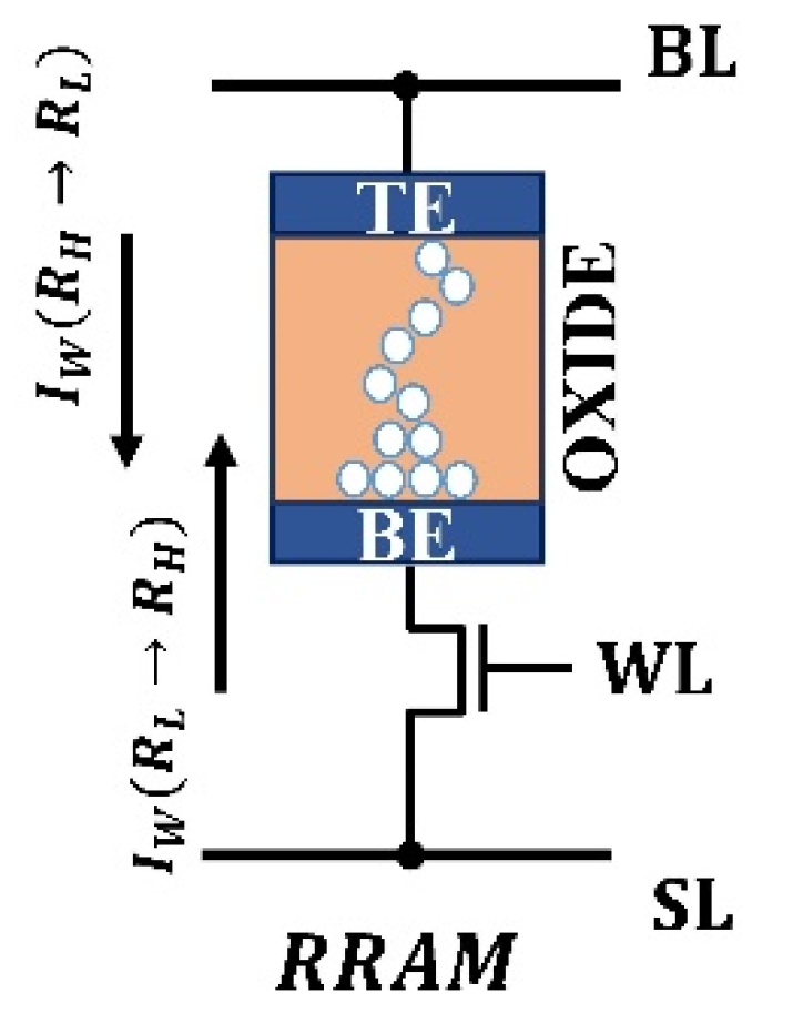
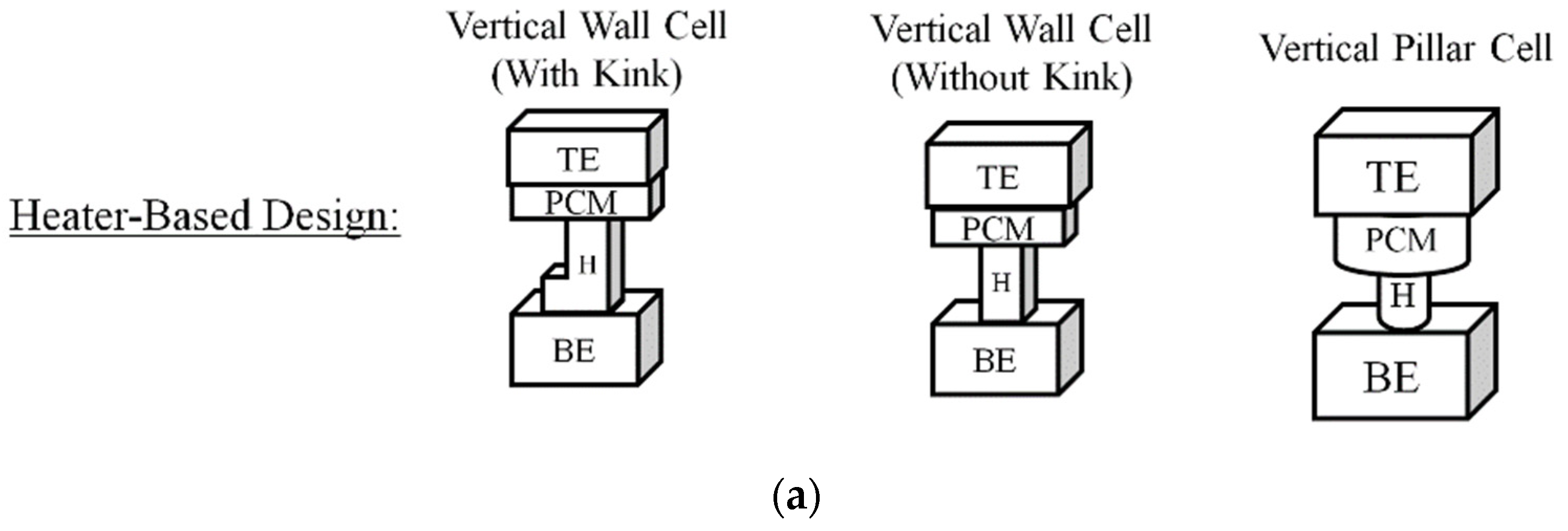
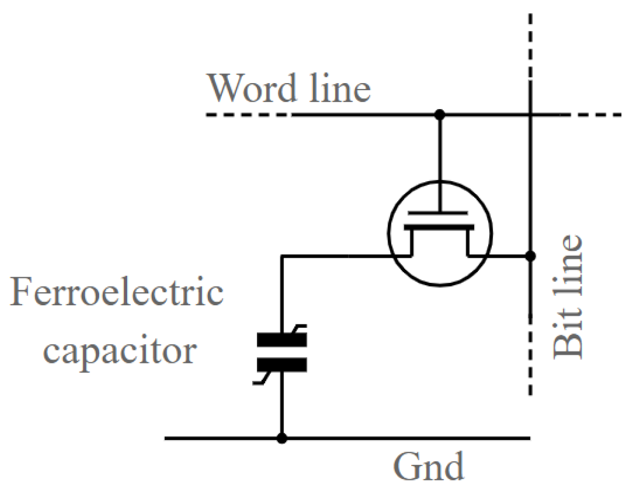
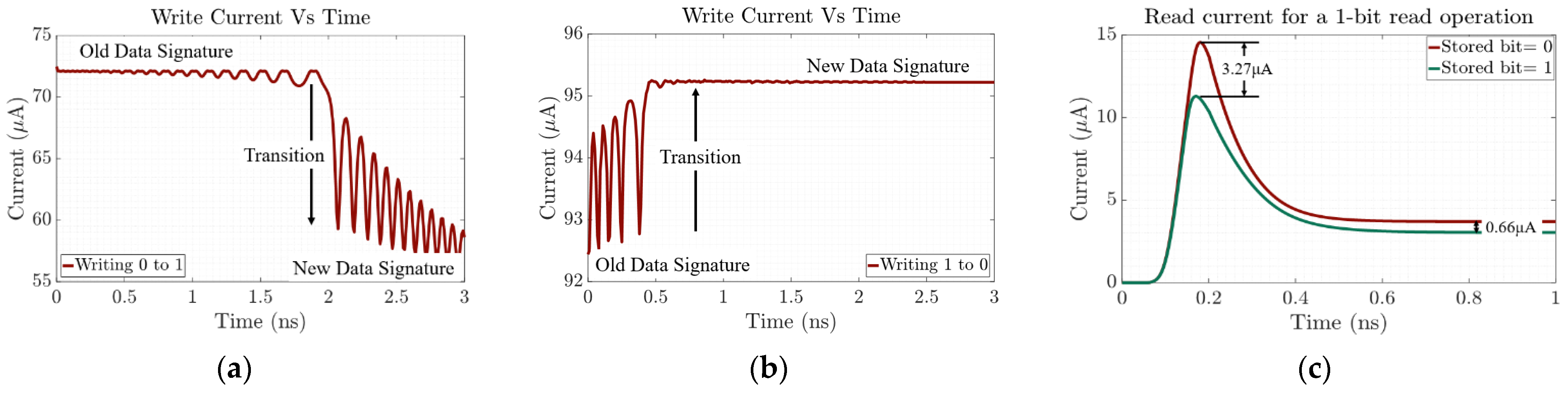
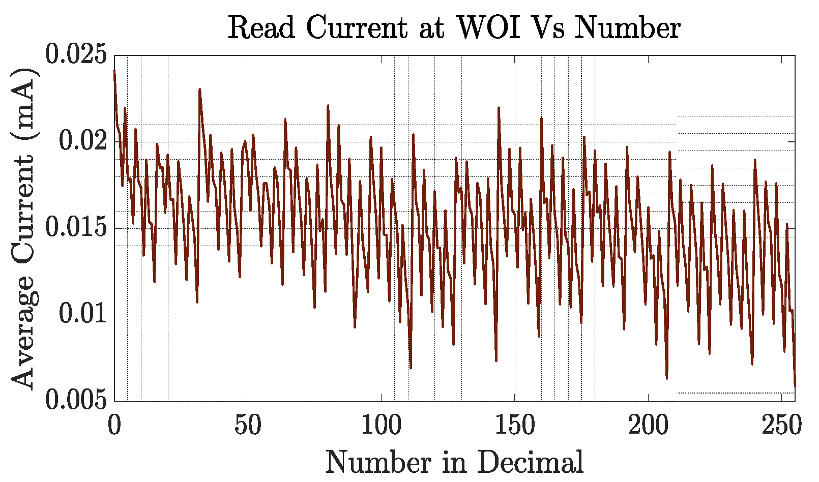
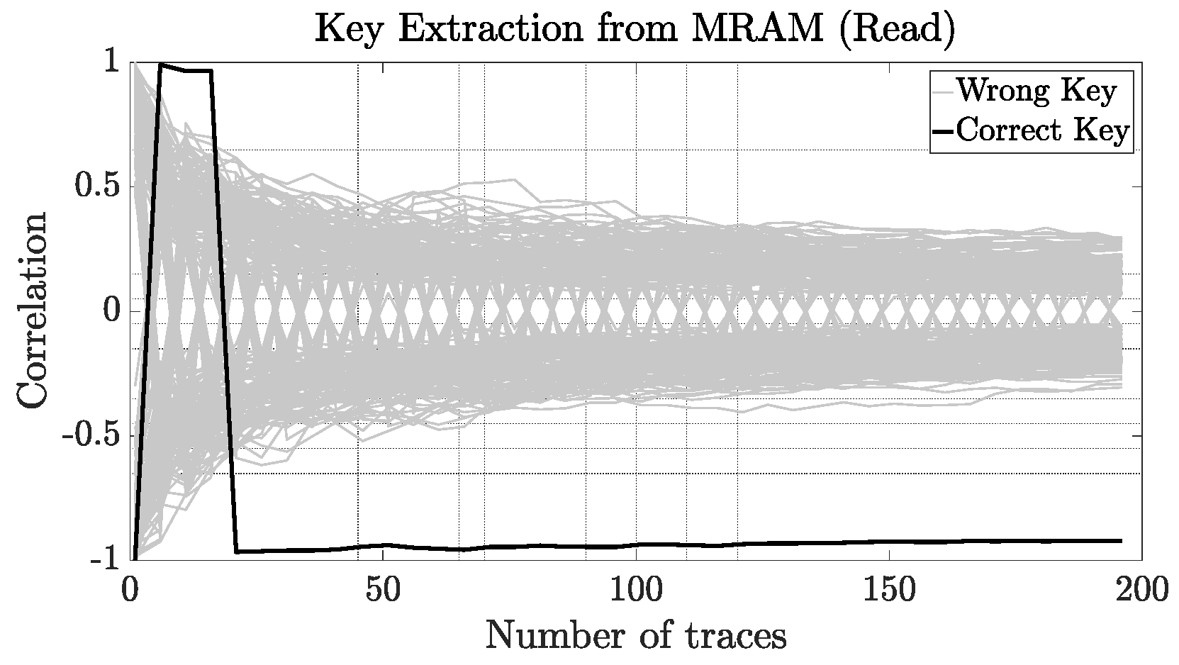
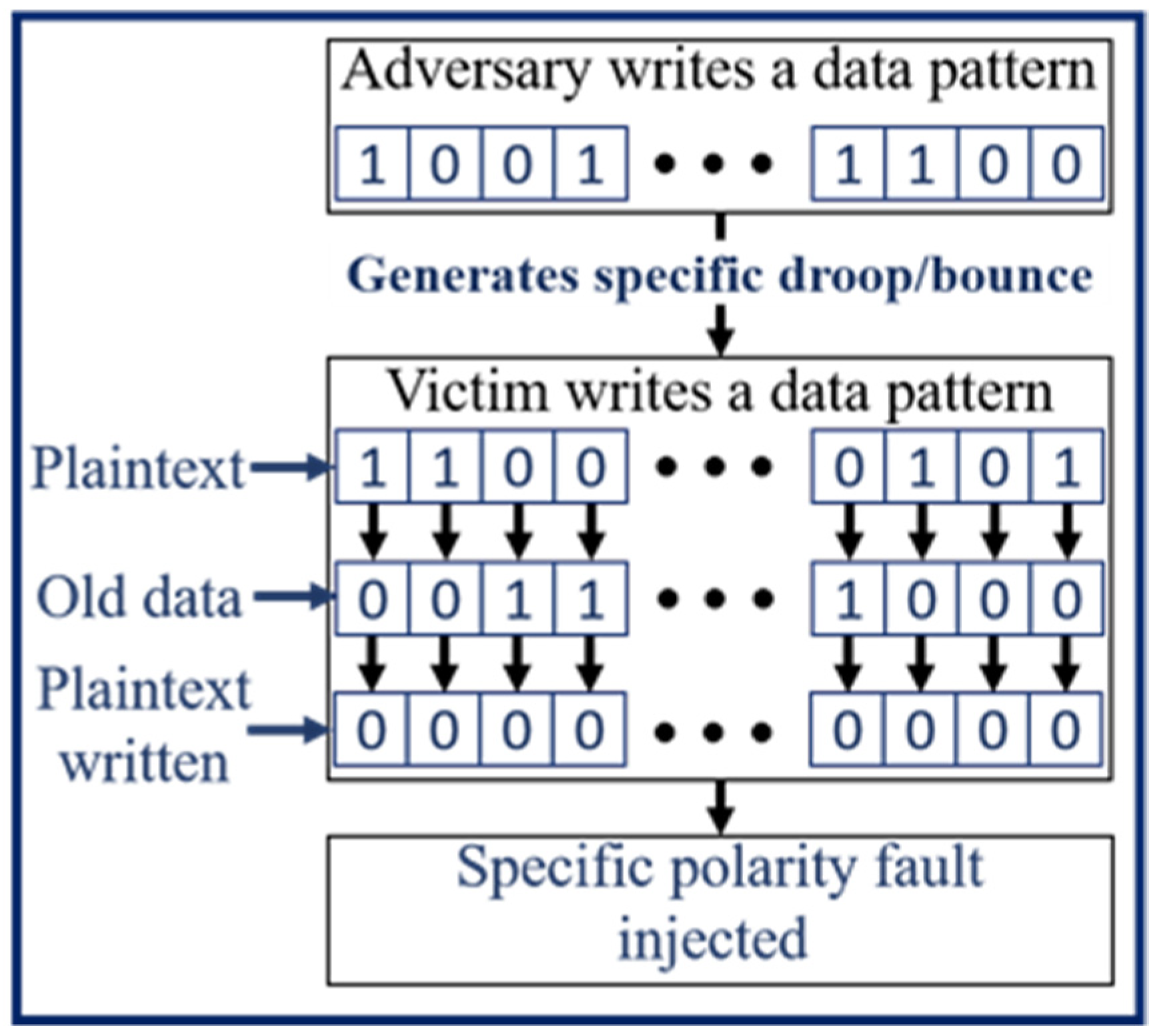
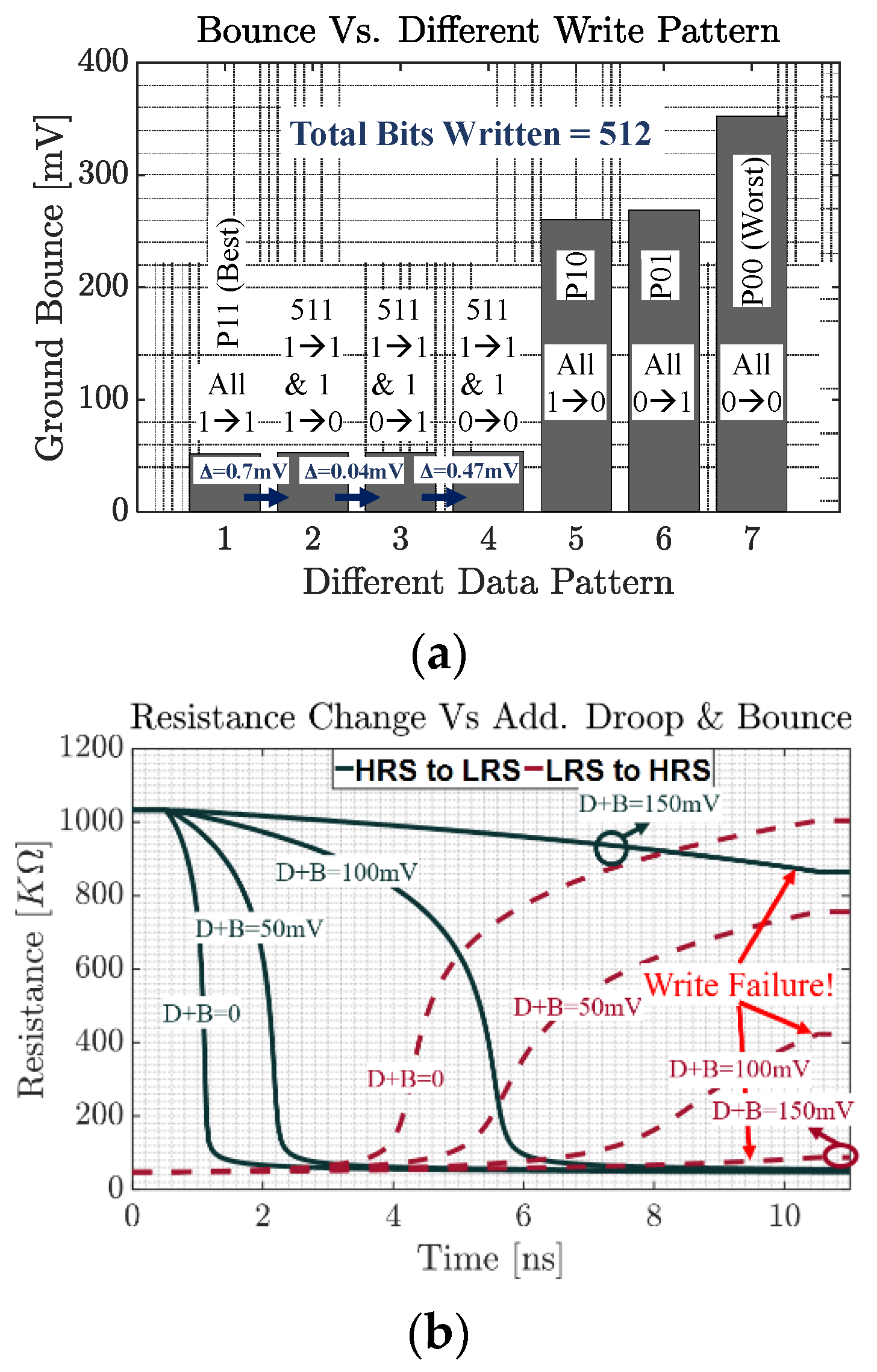
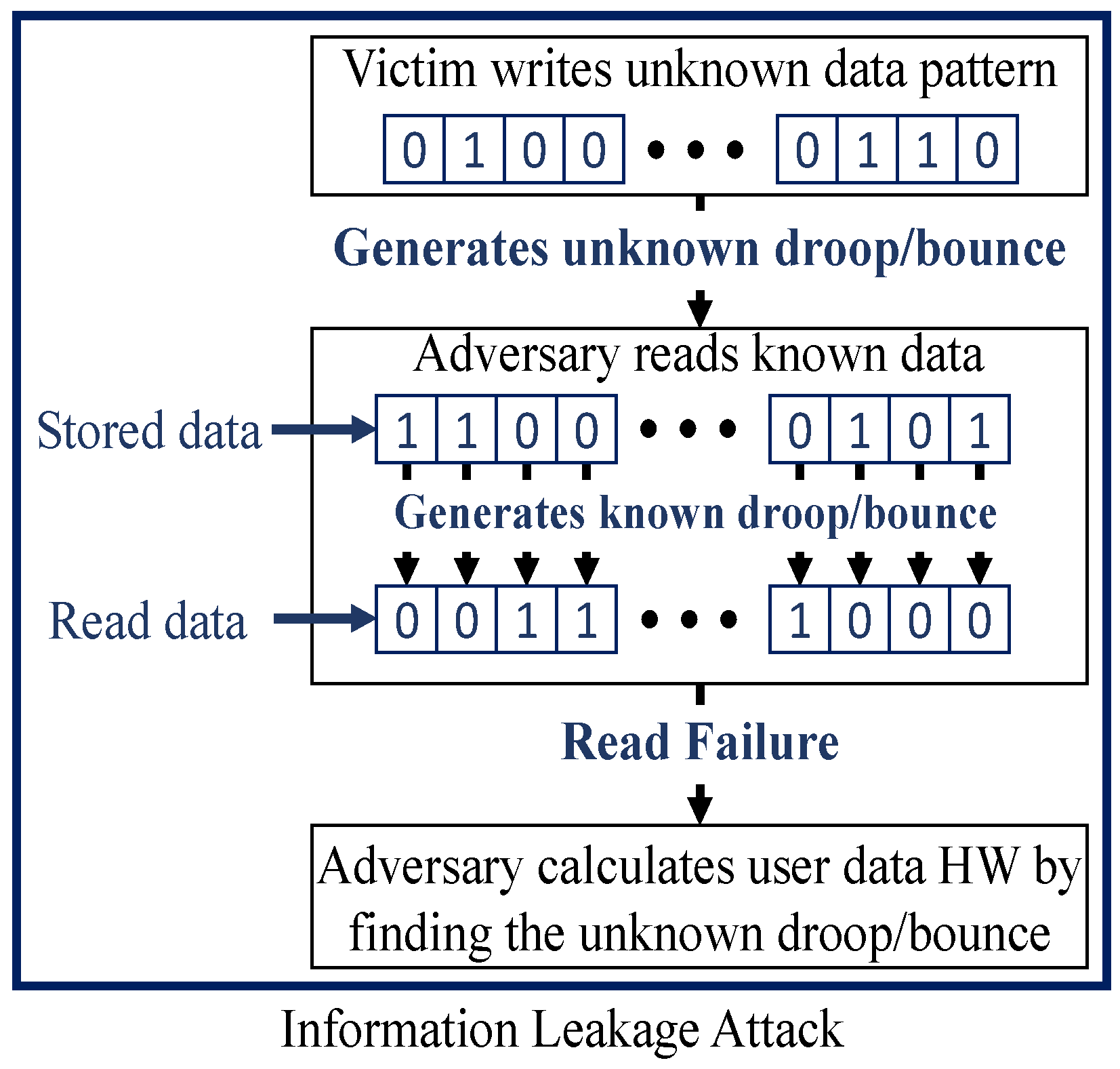
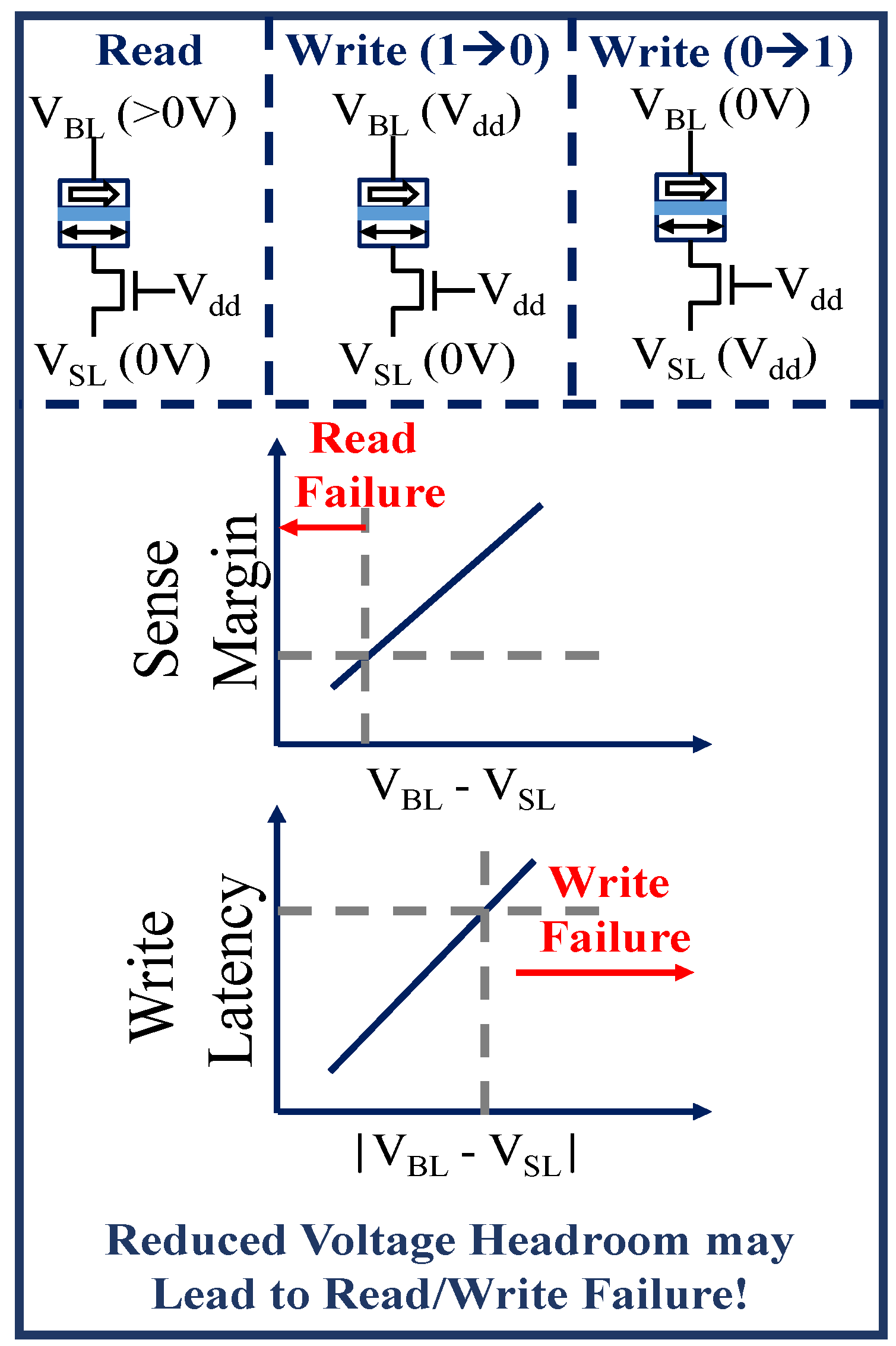
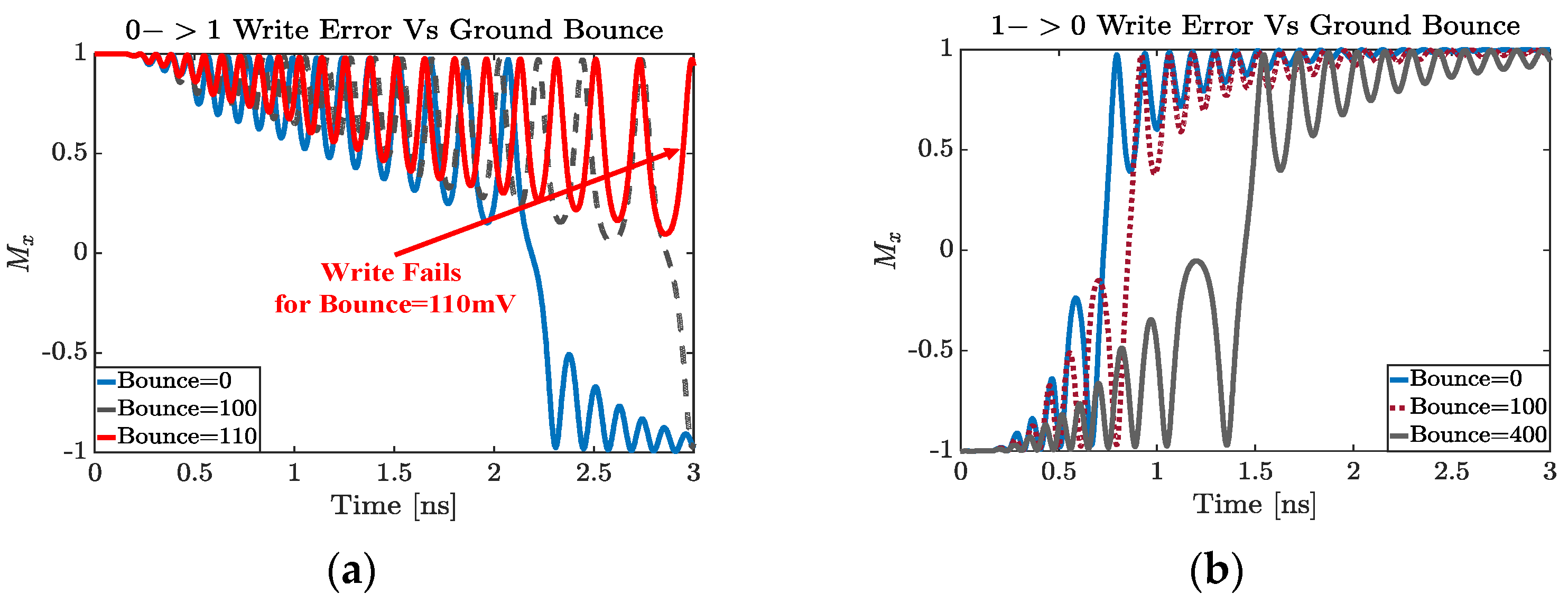
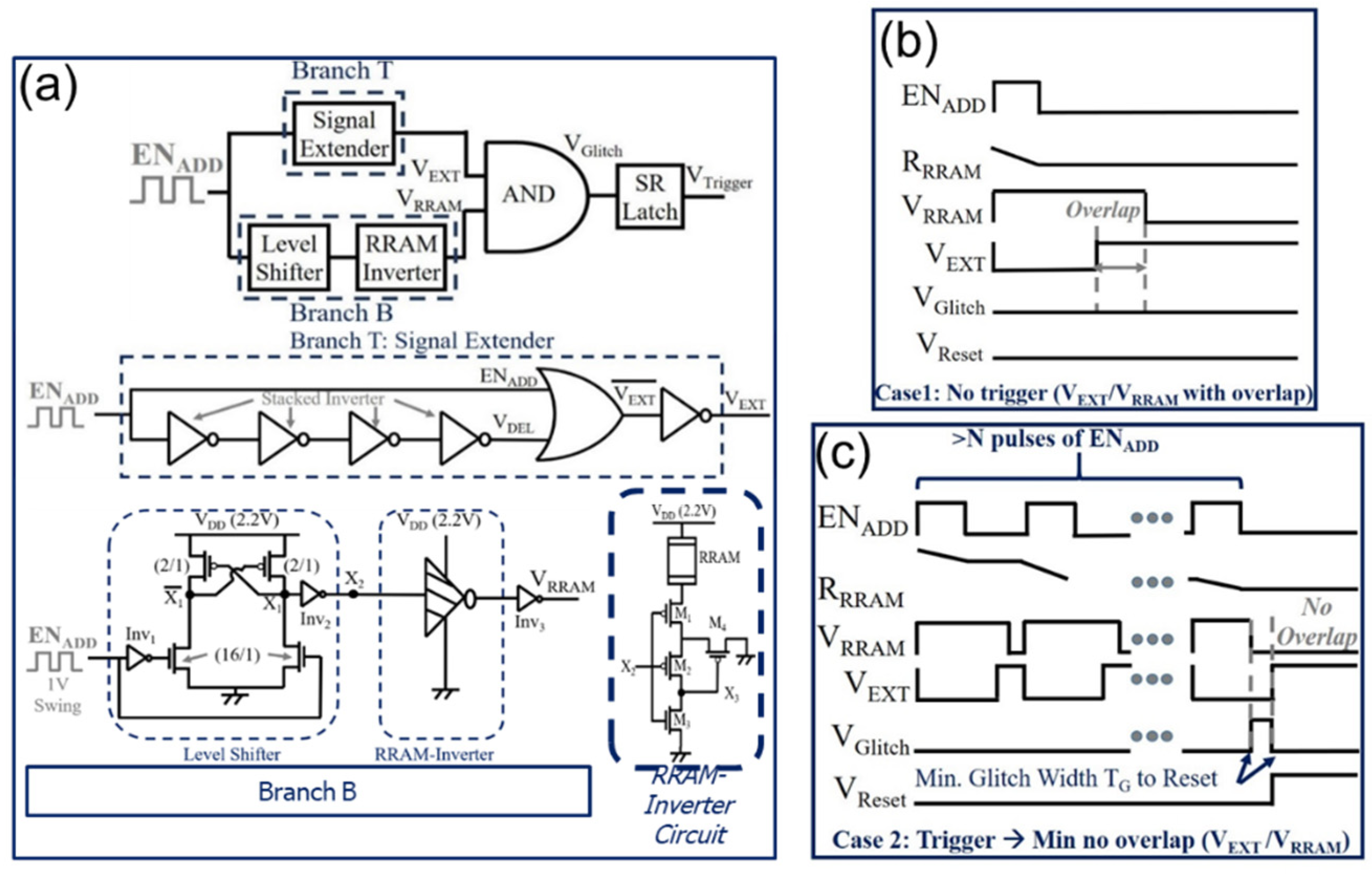
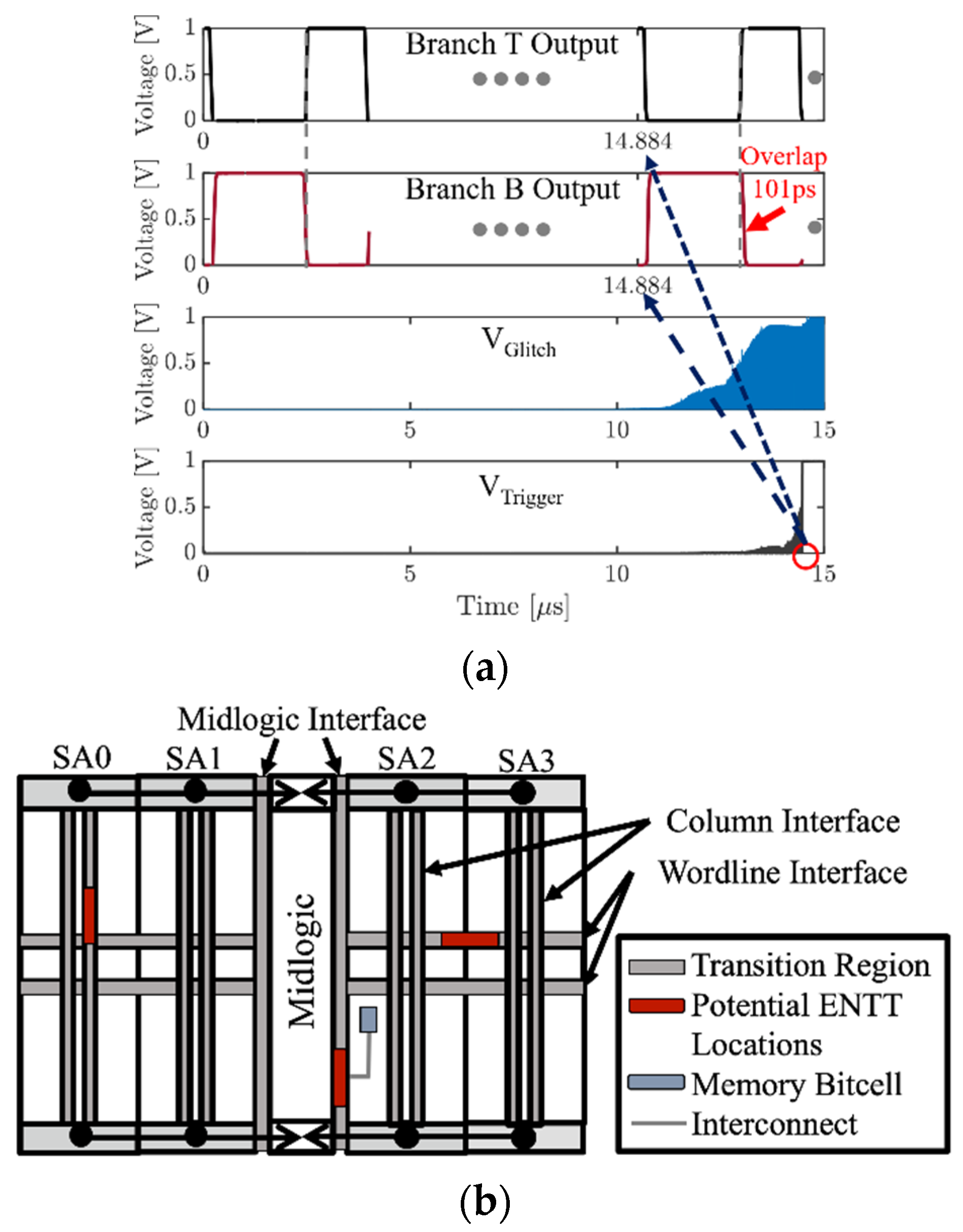
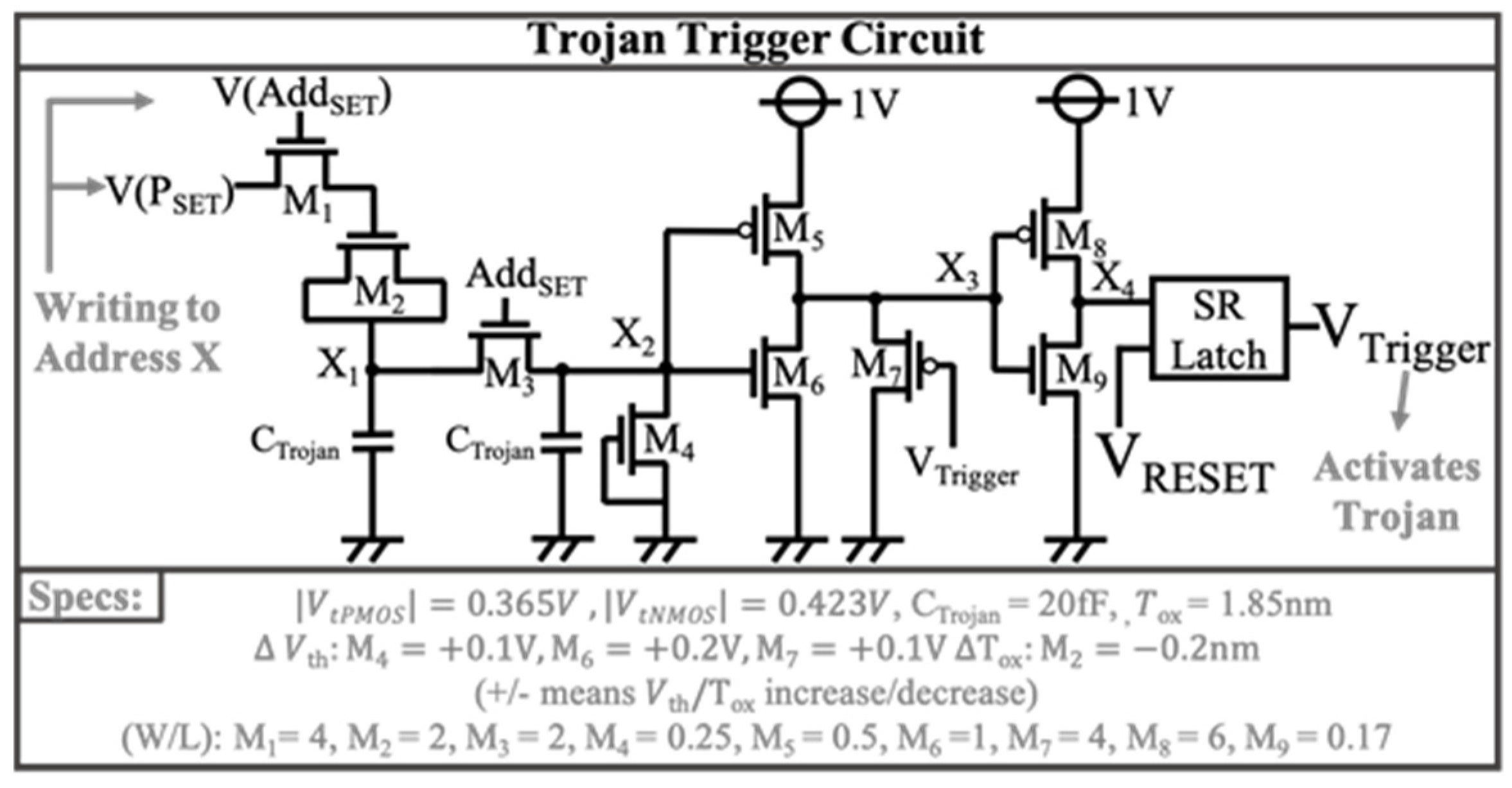
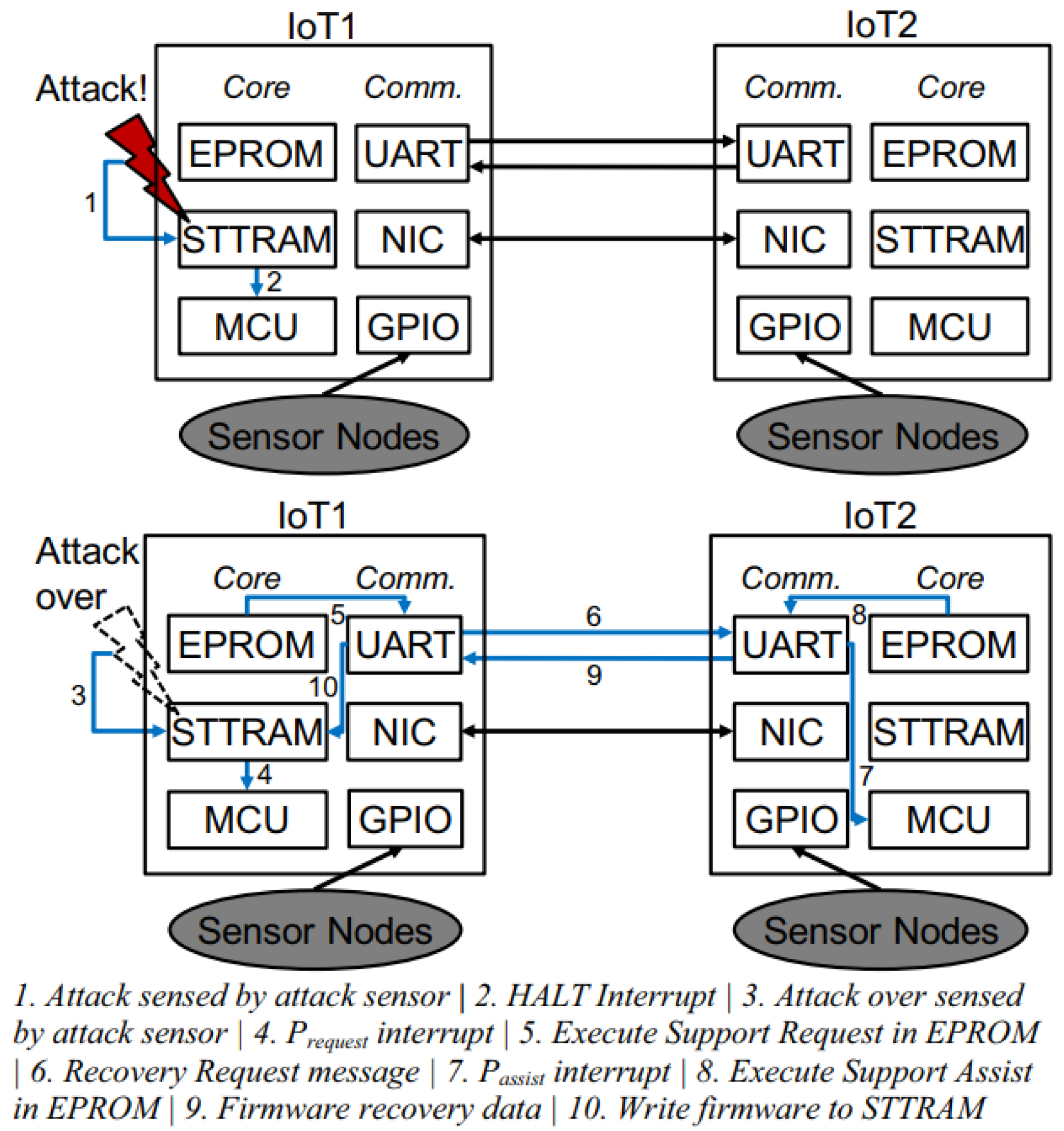
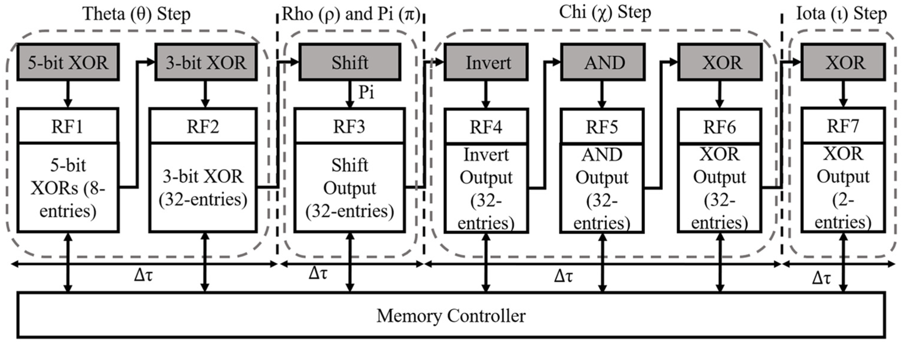
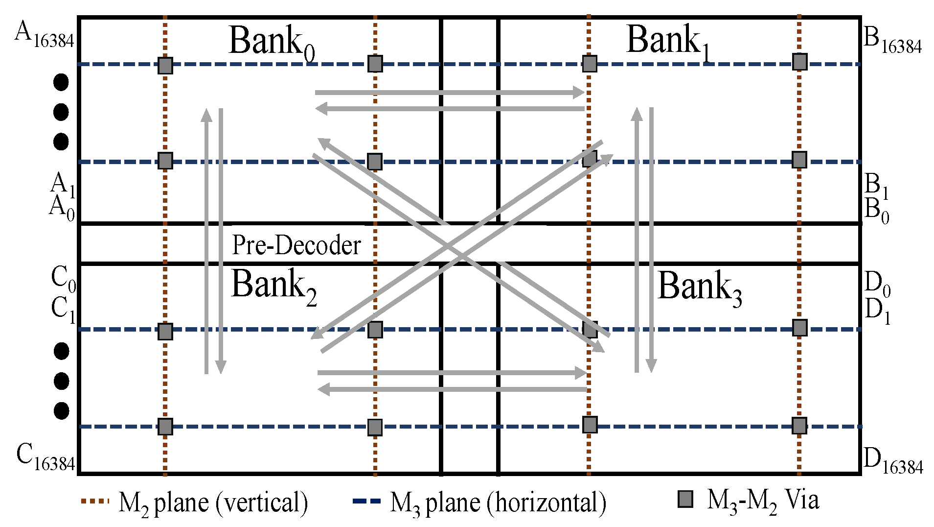
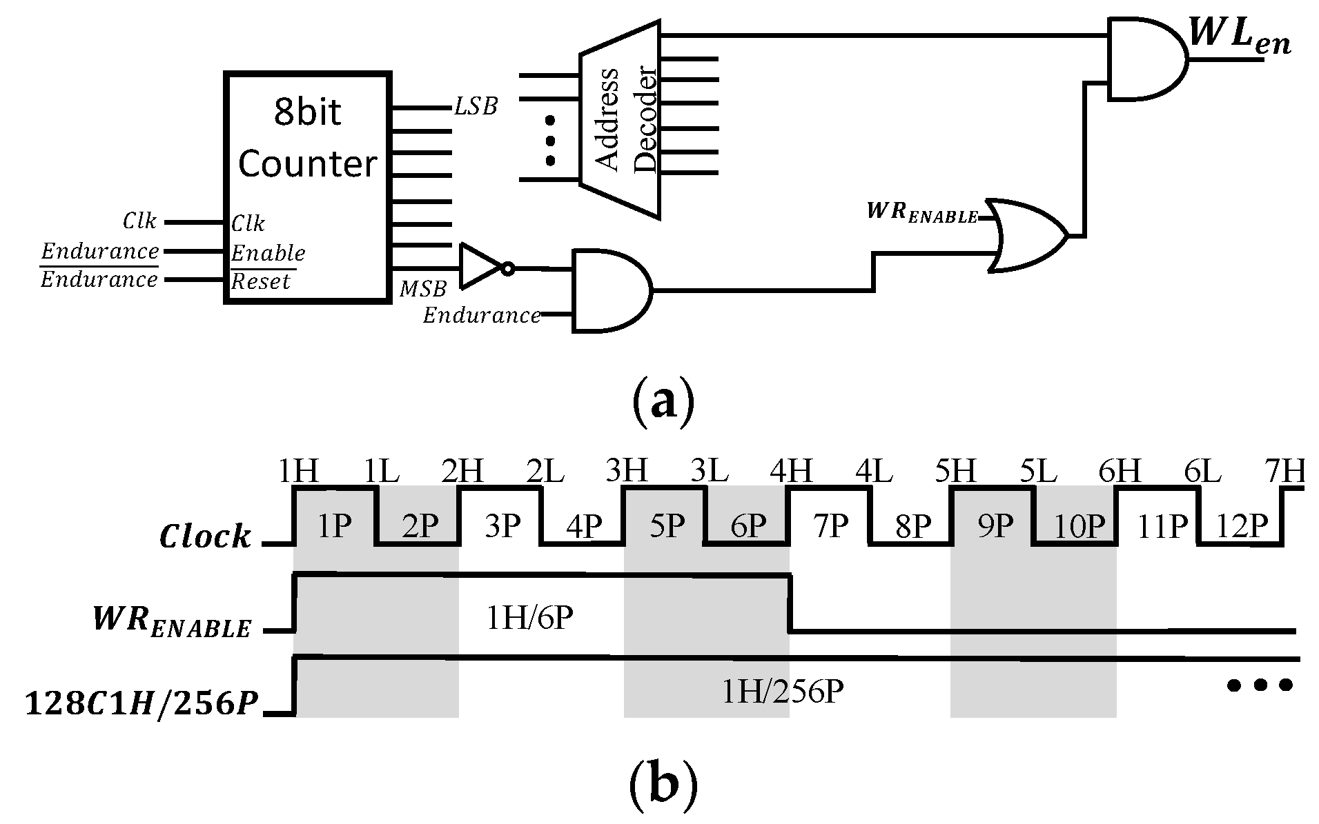
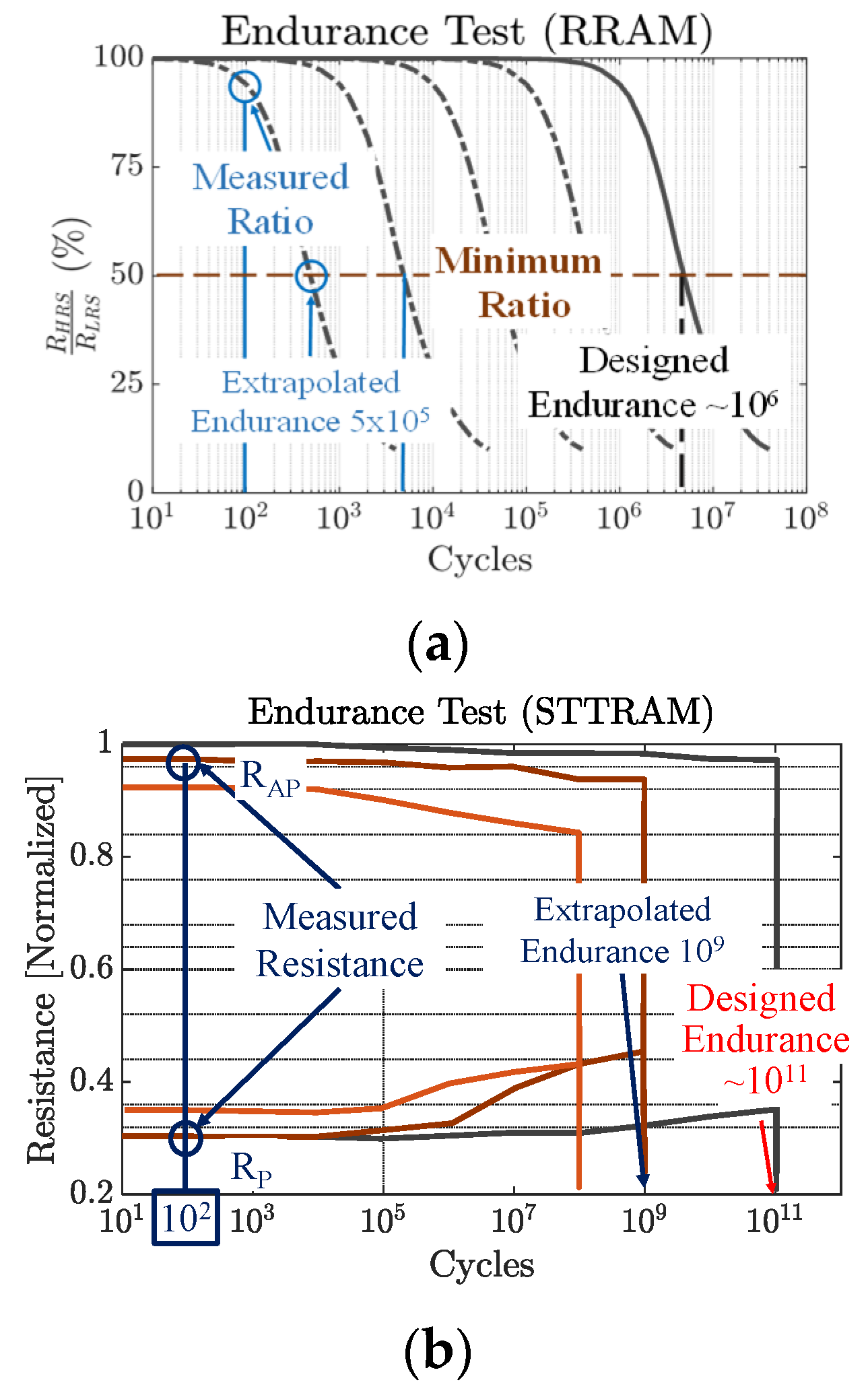
Table 1.
Comparative analysis of susceptibility of different NVMs and existing memory technologies to different data privacy and data security attacks.
Table 1.
Comparative analysis of susceptibility of different NVMs and existing memory technologies to different data privacy and data security attacks.
| Susceptible to | ||||||||
|---|---|---|---|---|---|---|---|---|
| Data Privacy | Data Security | |||||||
| Side Channel Attack | Fault Injection Attack | Information Leakage Attack | Row Hammer Attack | DoS Attack | Thermal Attack | Magnetic Attack | Electric Field Attack | |
| SRAM | ✓ | |||||||
| DRAM | ✓ | |||||||
| Flash | ✓ | |||||||
| STTRAM | ✓ | ✓ | ✓ | ✓ | ✓ | ✓ | ✓ | |
| MRAM | ✓ | ✓ | ✓ | ✓ | ✓ | ✓ | ✓ | |
| RRAM | ✓ | ✓ | ✓ | ✓ | ✓ | ✓ | ||
| PCM | ✓ | ✓ | ✓ | ✓ | ✓ | ✓ | ||
| FeRAM | ✓ | ✓ | ✓ | ✓ | ||||
Publisher’s Note: MDPI stays neutral with regard to jurisdictional claims in published maps and institutional affiliations. |
© 2021 by the authors. Licensee MDPI, Basel, Switzerland. This article is an open access article distributed under the terms and conditions of the Creative Commons Attribution (CC BY) license (https://creativecommons.org/licenses/by/4.0/).
Share and Cite
MDPI and ACS Style
Khan, M.N.I.; Ghosh, S. Comprehensive Study of Security and Privacy of Emerging Non-Volatile Memories. J. Low Power Electron. Appl. 2021, 11, 36. https://0-doi-org.brum.beds.ac.uk/10.3390/jlpea11040036
AMA Style
Khan MNI, Ghosh S. Comprehensive Study of Security and Privacy of Emerging Non-Volatile Memories. Journal of Low Power Electronics and Applications. 2021; 11(4):36. https://0-doi-org.brum.beds.ac.uk/10.3390/jlpea11040036
Chicago/Turabian StyleKhan, Mohammad Nasim Imtiaz, and Swaroop Ghosh. 2021. "Comprehensive Study of Security and Privacy of Emerging Non-Volatile Memories" Journal of Low Power Electronics and Applications 11, no. 4: 36. https://0-doi-org.brum.beds.ac.uk/10.3390/jlpea11040036
Note that from the first issue of 2016, this journal uses article numbers instead of page numbers. See further details here.