
0.5 V CMOS Inverter-Based Transconductance Amplifier with Quiescent Current Control


1
DIEEI (Dipartimento di Ingegneria Elettrica Elettronica e Informatica), University of Catania, 95125 Catania, Italy
2
DIET (Dipartimento di Ingegneria dell’Informazione Elettronica e Telecomunicazioni), Sapienza University of Rome, 00184 Rome, Italy
*
Author to whom correspondence should be addressed.
J. Low Power Electron. Appl. 2021, 11(4), 37; https://0-doi-org.brum.beds.ac.uk/10.3390/jlpea11040037
Submission received: 26 August 2021
/
Revised: 24 September 2021
/
Accepted: 27 September 2021
/
Published: 28 September 2021
(This article belongs to the Special Issue Ultra-Low-Power ICs for the Internet of Things)
Abstract
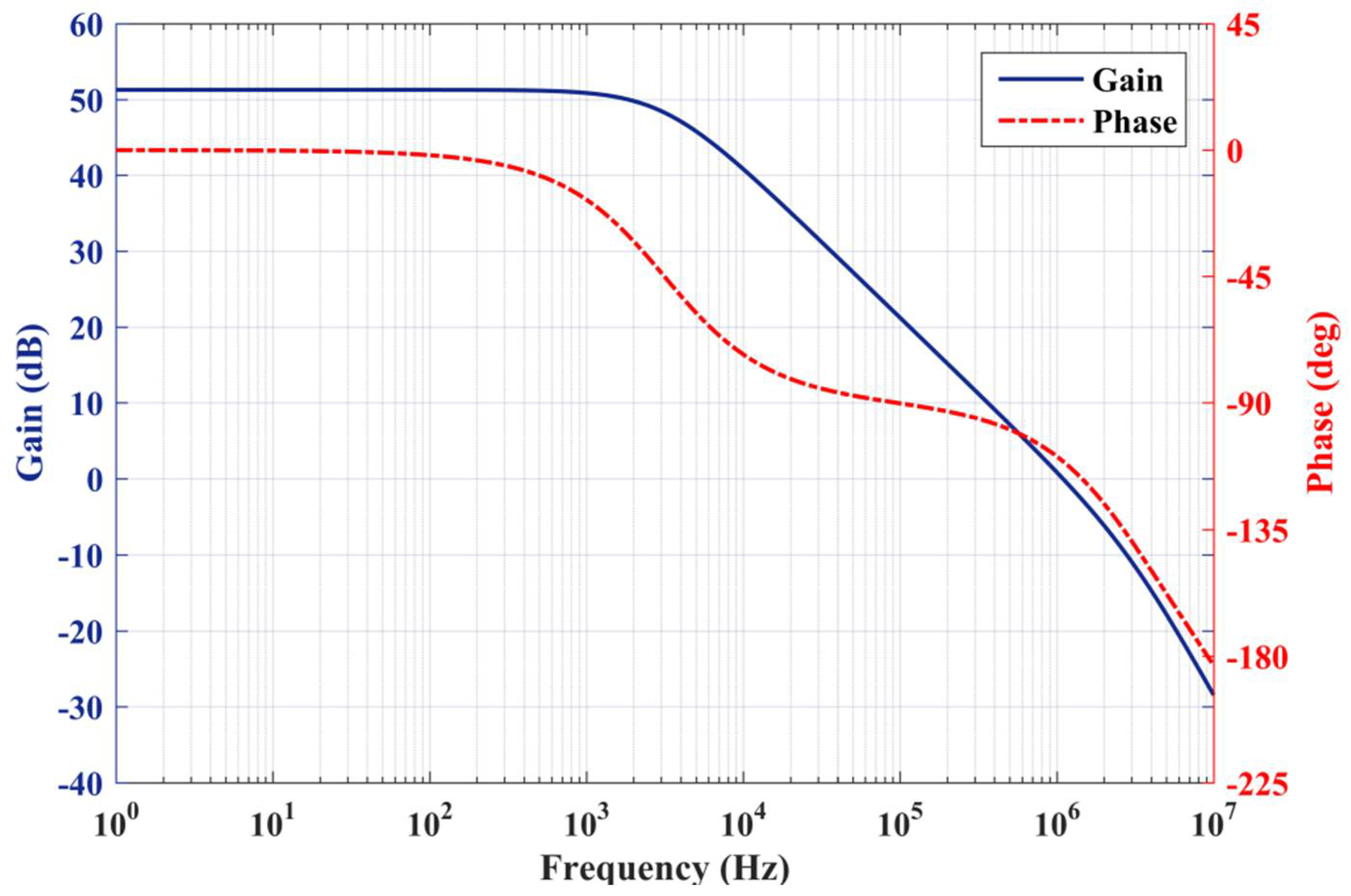
:A two-stage CMOS transconductance amplifier based on the inverter topology, suitable for very low supply voltages and exhibiting rail-to-rail output capability is presented. The solution consists of the cascade of a noninverting and an inverting stage, both characterized by having only two complementary transistors between the supply rails. The amplifier provides class-AB operation with quiescent current control obtained through an auxiliary loop that utilizes the MOSFETs body terminals. Simulation results, referring to a commercial 28 nm bulk technology, show that the quiescent current of the amplifier can be controlled quite effectively, even adopting a supply voltage as low as 0.5 V. The designed solution consumes around 500 nA of quiescent current in typical conditions and provides a DC gain of around 51 dB, with a unity gain frequency of 1 MHz and phase margin of 70 degrees, for a parallel load of 1 pF and 1.5 MΩ. Settling time at 1% is 6.6 μs, and white noise is 125 nV/.
1. Introduction
It is known that CMOS technology scaling, together with supply voltage reduction, is principally aimed at improving the performance of digital circuits and that, in this framework, the design of analog and mixed-signal blocks becomes increasingly demanding. It is indeed very difficult to obtain high linearity and high precision under near- and sub-threshold supply.
For this reason, operational transconductance amplifiers (OTAs) remain indispensable blocks for the implementation of high-accuracy closed-loop analog circuits, and several techniques have been proposed for the implementation of (ultra) low-voltage solutions. These include subthreshold-operated MOS transistors [1,2], bulk (body) driven [3,4], floating gate and quasi-floating gate MOS transistors [5,6], threshold lowering [7,8], level shifting [9], complementary pairs with body-driven gain boosting, and non-tailed pairs [10]. Additional approaches have also been proposed to replace OTAs, though not for general purpose usage, including dynamic amplifiers [11], ring amplifiers [12], and zero-crossing based circuits [13]. In addition, one interesting trend is the use of inverter-based topologies [14,15,16,17,18,19,20,21,22,23,24,25,26,27,28]. (A good review of the principal techniques for low-voltage OTAs can be found in the last reference.) At the basis of this approach is the single inverter (CMOS NOT gate), which is topologically simple, as it requires only two transistors between the supply rails, it provides a quite good voltage gain (though multi-stage topologies are usually required for 40 dB or more), and it exhibits class-AB and full swing operation. Therefore, it is rather effective under low supply voltages. However, the main drawback of the inverter-based solutions is related to the difficult control of the quiescent current feature that is especially required in low-power applications with a restricted current budget.
In this paper, a body-biasing technique, originally developed in [29] and utilized in [30], is applied to set the quiescent current of the generic inverter stage. Starting from this generic stage, a gate-driven, two-stage, inverter-based transconductance amplifier, suitable for switched-capacitor applications, is designed. Simulations results are also provided taking into account process and temperature variations. The proposed amplifier is designed in a 28-nm bulk process and is powered by a 0.5 V supply voltage. Typical quiescent current is 488 nA and, with a 1-pF//1.5-MΩ load, it provides 51-dB DC gain with a unity gain frequency of 1 MHz and phase margin of 70 degrees. Settling time at 1% is 6.6 μs and white noise is 125 nV/.
2. The Proposed Solution
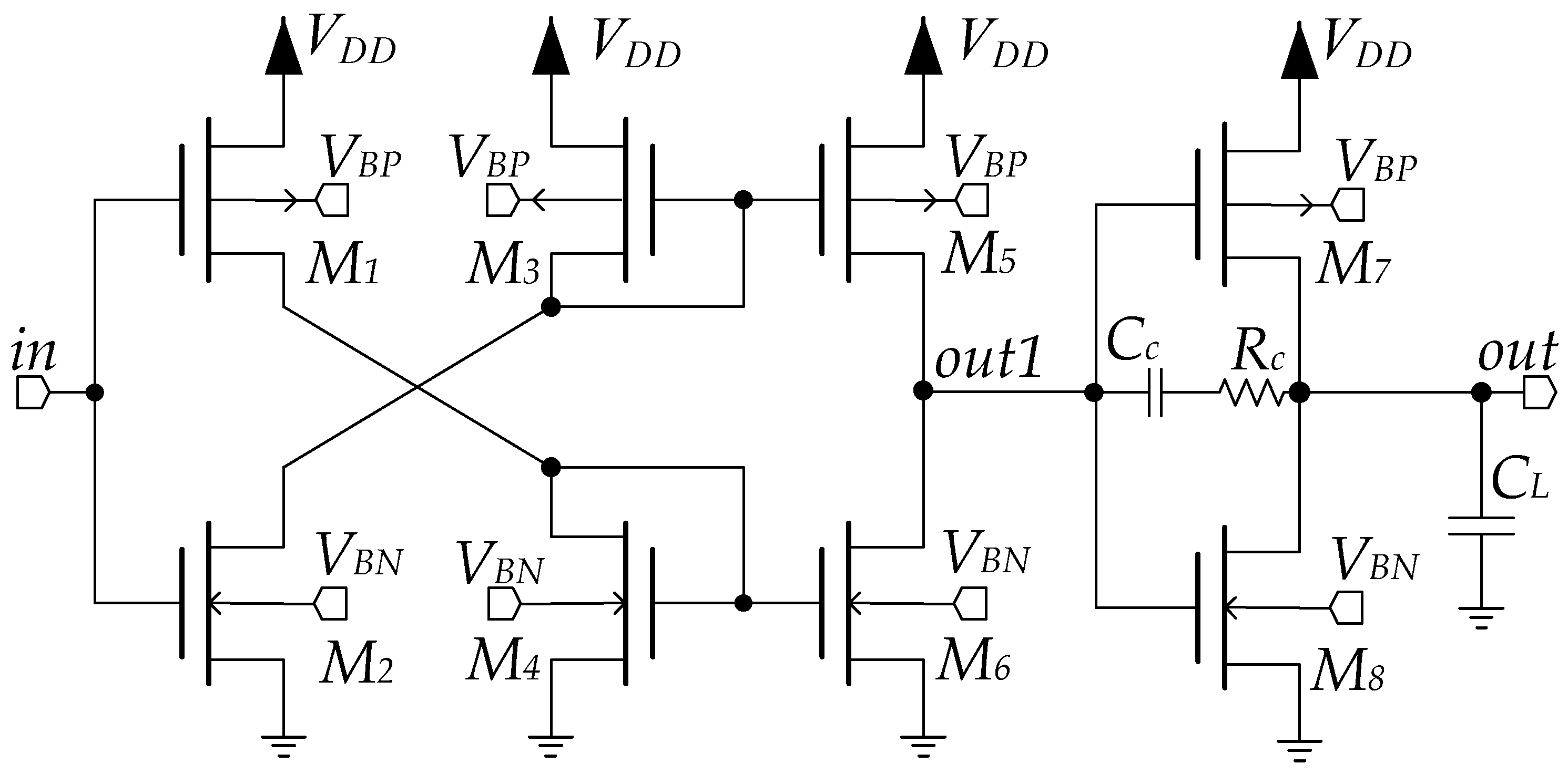
Figure 1 shows the circuit schematic of the proposed amplifier. It consists of a first noninverting stage, made up of transistors M1-M6, and a second inverting stage, made up of transistors M7-M8. As it is seen, the second stage is a straight CMOS NOT gate while the first one is based also onto the NOT topology, but rearranged to invert the gain trough two complementary p-channel and n-channel current mirrors M3, M5 and M4, M6. In quiescent conditions, the input terminal is set to VDD/2 and thanks to the overall negative feedback (not shown) also the output and intermediate node, out1, are all biased at VDD/2.
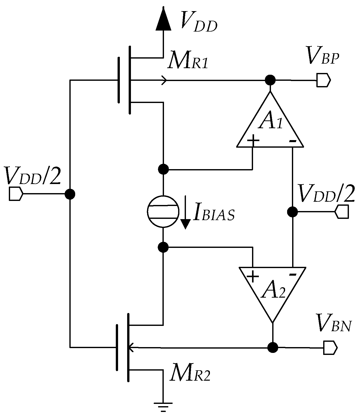
As far as the quiescent current control of the two stages is concerned, it is implemented through the bulk terminals via voltage VBP, for p-channel transistors, and VBN, for the n-channel ones. These voltages are generated by exploiting a technique proposed in [29] and utilized also in [10,30]. The basic working principle can be inferred with the aid of Figure 2, showing the simplified schematic of the amplifier’s biasing section.
MR1 and MR2 are two reference transistors both with their |VGS| equal to VDD/2. Their quiescent drain current is equal to IBIAS thanks to the local feedback loop operated by the auxiliary amplifiers A1 and A2, which generate the required bulk voltages, VBP and VBN, under the following summarized constraints:
- (a)
- assigned aspect ratios (W/L)R1 and (W/L)R2;
- (b)
- ID1,2 = kIBIAS, where k is the ratio of the transistors aspect ratio as in (1);
- (c)
- VSGR1 = VGSR2 = VDD/2;
- (d)
- VSDR1 = VDSR2 = VDD/2, assuming ideal input virtual short in A1 and A2.
Of course, aspect ratios of MR1 and MR2 must be set so that the required bulk voltages are within VDD and ground. Moreover, the auxiliary amplifiers A1 and A2 should provide a maximum (rail-to-rail) output voltage range, whereas input common mode range is not a concern as input voltage is kept constant to VDD/2. Therefore, simple two-stage OTAs biased in subthreshold can be profitably used. An example of implementation of this type of amplifier is found in [10], albeit operating with MOSFETs in saturation.
Consider now transistor M1 of the main amplifier in Figure 1 and remember that in quiescent conditions Vin is equal to VDD/2. As a consequence, MR1 and M1 have respectively the same source, gate, and bulk voltage and hence the drain current of M1 is related to that of MR1 in a mirror-like condition
where equality is accurately verified because the source-drain voltage of M1 is also equal to VDD/2, thanks to the diode-connected transistor M4 in Figure 1 which absorbs ID1 and is designed so that
and consequently VGS4 = VDD/2.
Similar considerations hold for all the transistors in the main amplifier, in practice, all p-channel and n-channel devices have their current linked to IBIAS via the current-mirror-like relations
where (W/L)i_P (i = 1,3,5,7) and (W/L)j_N (j = 2,4,6,8) are respectively the aspect ratios of the generic p-channel and n-channel MOSFET in the main amplifier.
As a concluding remark, closed loop stability is ensured thanks to the conventional frequency compensation network made up of the Miller capacitor, CC, and nulling resistor, RC, around the last inverting stage.
3. Validation Results
The proposed solution was designed in a 28-nm triple-well CMOS technology provided by STMicroelectronics and simulated at the schematic level. Threshold voltages of the n- and p-channel devices were 445 mV and −462 mV, respectively. Single power supply was set to 0.5 V, IBIAS was 60 nA, and transistor dimensions, together with other component values, were set as summarized in Table 1. All p-channel (n-channel) MOSFETS are equal to the reference device 990/90 (210/90) nm/nm, except for the last stage transistors that have four times greater aspect ratios. This is important to increase the output current drive capability and the output transconductance to reduce the required value of the nulling resistor (to avoid introducing a positive zero), whose value is in the range of 1/gm2. Observe that the DC gain of the auxiliary amplifiers, A1 and A2, is around 40 dB. As a consequence of the transistor’s dimension, the nominal quiescent current in each branch of the first stage is 60 nA, while it is 240 nA in the last stage, resulting in a total nominal quiescent current of 420 nA. The small-signal parameters of the amplifier stages are summarized in Table 2. Load capacitor CL was 1 pF in parallel to a load resistor of 1.5 MΩ, and the compensation capacitor and the nulling resistor were set to 1.5 pF and 50 kΩ, respectively.
The robustness of the quiescent conditions were validated at first. The nominal bulk voltages, VBP and VBN, generated by a circuit in Figure 2 were 256.4 mV and 231.9 mV, respectively. The simulated quiescent current in the main amplifier in Figure 1 was 488 nA, on average, with a standard deviation of 93.7 nA, after running 1000 Monte Carlo iterations. The difference with respect to the expected value of 420 nA is due to the low DC gains of the auxiliary amplifiers, which cause a closed-loop gain error.
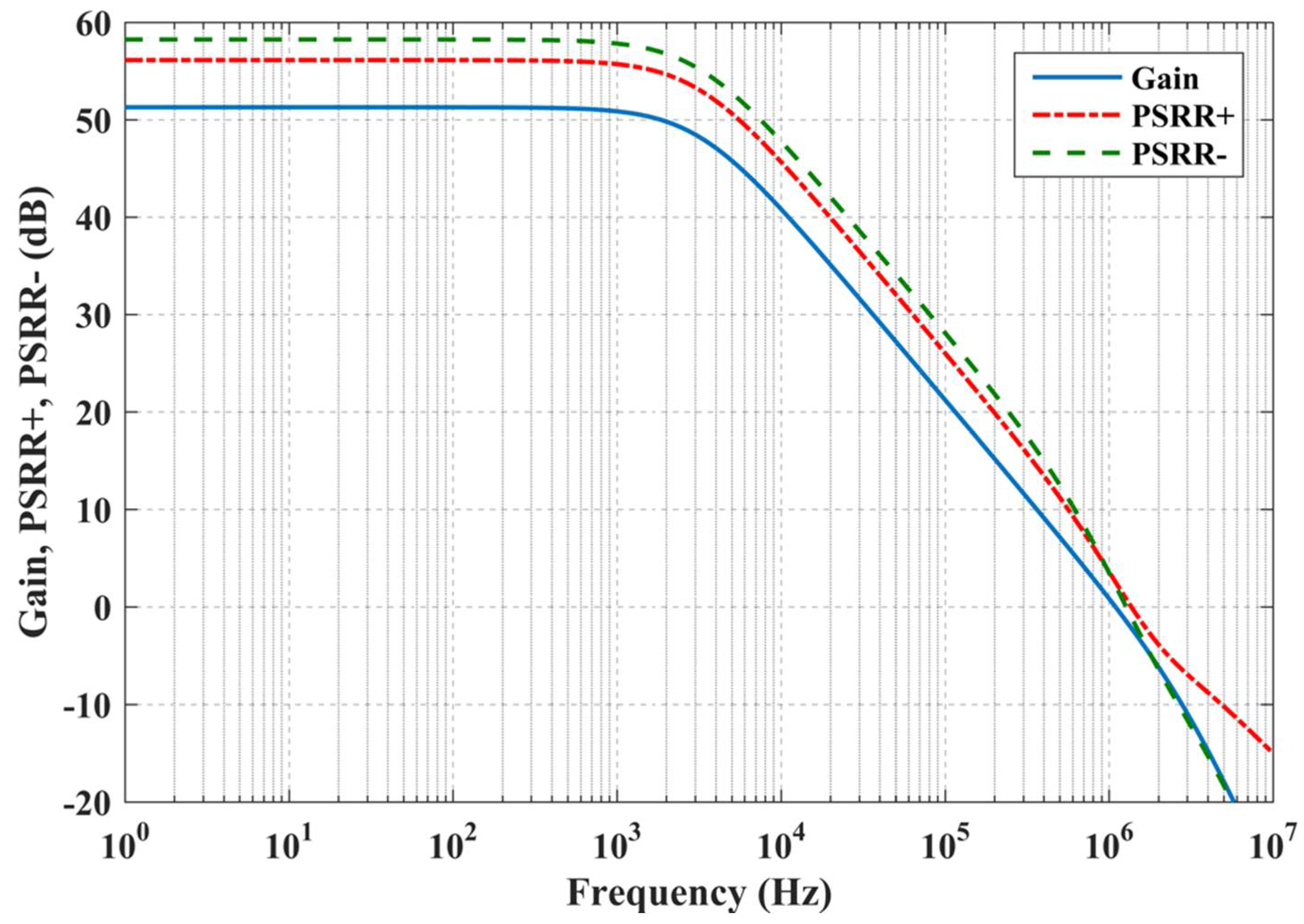
Figure 3 shows the Bode plots (magnitude and phase) of the amplifier open-loop gain at the standard temperature (27 °C) and nominal component models with a 1-pF and 1.5-MΩ parallel load. DC gain is 51 dB, unity gain frequency (UGF) is 1 MHz and phase margin (PM) is 70 degrees. Note that the load resistance is almost equal to ro2 in Table 2, hence causing a 6-dB reduction in the maximum achievable gain.
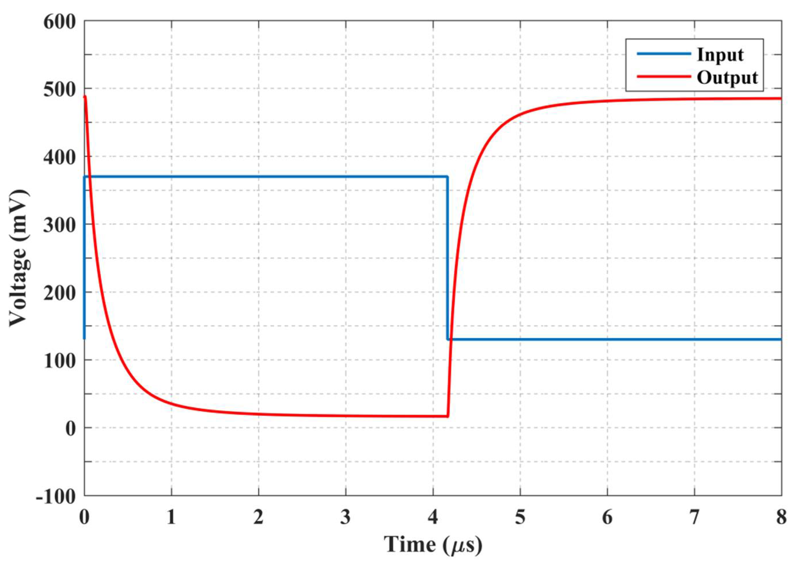
Figure 4 shows the time transient response of the amplifier with the closed-loop gain set to −2. These plots are achieved with two feedback resistors, as in an inverting closed-loop amplifier topology, one of 1 MΩ (connected between the input and output) and the other of 0.5 MΩ (connected between the signal source and the input). The almost rail-to-rail output behavior is apparent. Positive/negative settling time at 1% of the final value is symmetrical and equal to 6.6 μs.
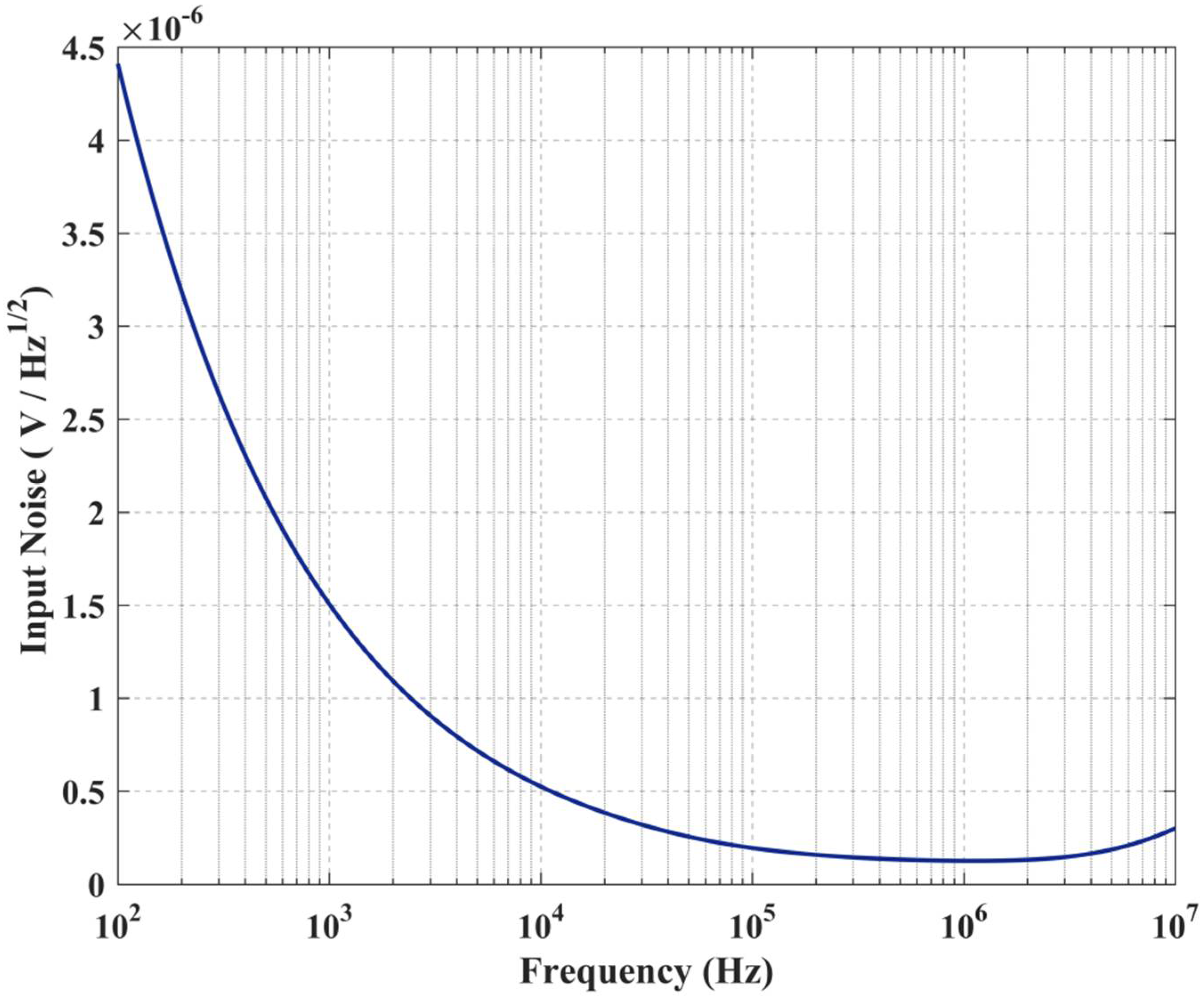
Power Supply Rejection Ratio was also evaluated from both supply rails. Magnitude versus frequency of PSRR is shown in Figure 5. PSRR+ was 56 dB at DC, while PSRR– was 58 dB. Equivalent input noise is also simulated and depicted in Figure 6. The white component is 125 nV/ and is dominated by the voltage noise of transistors M1–M6 forming the input stage.
The effect of mismatches was also simulated through 1000 Monte Carlo iterations. Table 3 summarizes the results. The largest variation is experienced by the unity gain frequency and settling times (more than 30%).
Temperature and process variations were also evaluated via corner simulations under three different temperatures (−20 °C, +27 °C and +85 °C). Results are summarized in Table 4. It is seen that the quiescent current is sensitive to temperature and to FF and SS corners. In particular, the total amplifier nominal current (which was approximately 488 nA) decreases to 249 nA at −20 °C, SS corner, and increases to 2.4 μA at +80 °C, FF corner. DC gain, PM and PSRR exhibit only quite negligible changes, whereas UGF and settling time are affected by these standby current variations. This problem is mainly related to the large threshold voltage excursion induced by temperature variation that cannot be counteracted by the restricted range of the bulk control voltages limited to VDD.
4. Conclusions
A novel inverter-based two-stage CMOS transconductance amplifier, with quiescent current control and suitable for very low supply voltages was presented. The solution consists of the cascade of a noninverting and an inverting stage both characterized by having only two complementary transistors between the supply rails, thus providing rail-to-rail and class-AB output capability. The designed solution is supplied from 0.5 V and in quiescent conditions consumes (typically) approximately 488 nA, while providing a DC gain of approximately 51 dB, with a unity gain frequency of 1 MHz and phase margin of 70 degrees, for a 1-pF//1.5-MΩ load.
The quiescent current control loop proved to be effective against mismatches and process variations. Further investigation is currently being carried out to reduce the quiescent current sensitivity to temperature. This drawback is caused by the limited variation allowed to the body biasing control voltage, which is of course restricted to VDD and ground. Once VBP and VBN reach these limits and saturate, the control loop becomes ineffective. For this reason, making IBIAS with a coefficient negative to absolute temperature (NTAT) could be a favorable solution and subject for further study.
Author Contributions
Conceptualization: S.P. and G.S.; data curation: A.B.; original draft preparation: S.P. and A.B.; writing—review and editing: all authors; supervision: S.P. and G.S. All authors have read and agreed to the published version of the manuscript.
Funding
This research received no external funding.
Data Availability Statement
The data presented in this study are available in article.
Conflicts of Interest
The authors declare no conflict of interest.
References
- Vittoz, E.; Fellrath, J. CMOS analog integrated circuits based on weak inversion operations. IEEE J. Solid-State Circuits 1977, 12, 224–231. [Google Scholar] [CrossRef] [Green Version]
- Kumar, A.R.A.; Sahoo, B.D.; Dutta, A. A Wideband 2–5 GHz Noise Canceling Subthreshold Low Noise Amplifier. IEEE Trans. Circuits Syst. II Express Briefs 2018, 65, 834–838. [Google Scholar] [CrossRef]
- Zuo, L.; Islam, S.K. Low-Voltage Bulk-Driven Operational Amplifier With Improved Transconductance. IEEE Trans. Circuits Syst. I Regul. Pap. 2013, 60, 2084–2091. [Google Scholar] [CrossRef]
- Akbari, M.; Hussein, S.M.; Hashim, Y.; Tang, K.-T. An Enhanced Input Differential Pair for Low-Voltage Bulk-Driven Amplifiers. IEEE Trans. Very Large Scale Integr. (VLSI) Syst. 2021, 29, 1601–1611. [Google Scholar] [CrossRef]
- Ramirez-Angulo, J.; Lopez-Martin, A.; Carvajal, R.; Chavero, F. Very low-voltage analog signal processing based on quasi-floating gate transistors. IEEE J. Solid-State Circuits 2004, 39, 434–442. [Google Scholar] [CrossRef]
- Miguel, J.M.A.; Lopez-Martin, A.J.; Acosta, L.; Ramirez-Angulo, J.; Carvajal, R.G. Using Floating Gate and Quasi-Floating Gate Techniques for Rail-to-Rail Tunable CMOS Transconductor Design. IEEE Trans. Circuits Syst. I Regul. Pap. 2011, 58, 1604–1614. [Google Scholar] [CrossRef]
- Lehmann, T.; Cassia, M. 1-V power supply CMOS cascode amplifier. IEEE J. Solid-State Circuits 2001, 36, 1082–1086. [Google Scholar] [CrossRef]
- Chatterjee, S.; Tsividis, Y.; Kinget, P. 0.5-V analog circuit techniques and their application in OTA and filter design. IEEE J. Solid-State Circuits 2005, 40, 2373–2387. [Google Scholar] [CrossRef]
- Carrillo, J.; Duque-Carrillo, J.; Torelli, G.; Ausin, J. Constant-gm constant-slew-rate high-bandwidth low-voltage rail-to-rail CMOS input stage for VLSI cell libraries. IEEE J. Solid-State Circuits 2003, 38, 1364–1372. [Google Scholar] [CrossRef]
- Grasso, A.D.; Pennisi, S.; Scotti, G.; Trifiletti, A. 0.9-V Class-AB Miller OTA in 0.35-µm CMOS With Threshold-Lowered Non-Tailed Differential Pair. IEEE Trans. Circuits Syst. I Regul. Pap. 2017, 64, 1740–1747. [Google Scholar] [CrossRef]
- Lin, J.; Paik, D.; Lee, S.; Miyahara, M.; Matsuzawa, A. An Ultra-Low-Voltage 160 MS/s 7 Bit Interpolated Pipeline ADC Using Dynamic Amplifiers. IEEE J. Solid-State Circuits 2015, 50, 1399–1411. [Google Scholar] [CrossRef]
- Lim, Y.; Flynn, M.P. A 100 MS/s, 10.5 Bit, 2.46 mW Comparator-Less Pipeline ADC Using Self-Biased Ring Amplifiers. IEEE J. Solid-State Circuits 2015, 50, 2331–2341. [Google Scholar] [CrossRef]
- Lee, S.; Chandrakasan, A.P.; Lee, H.S. A 12 b 5-to-50 MS/s 0.5-to-1 V Voltage Scalable Zero-Crossing Based Pipelined ADC. IEEE J. Solid-State Circuits 2012, 47, 1603–1614. [Google Scholar] [CrossRef]
- Michel, F.; Steyaert, M.S.J. A 250 mV 7.5 W 61 dB SNDR SC ∆Σ Modulator Using Near-Threshold-Voltage-Biased Inverter Amplifiers in 130 nm CMOS. IEEE J. Solid-State Circuits 2012, 47, 709–721. [Google Scholar] [CrossRef]
- Yaul, F.M.; Chandrakasan, A.P. A Noise-Efficient 36 nV/Hz Chopper Amplifier Using an Inverter-Based 0.2-V Supply Input Stage. IEEE J. Solid-State Circuits 2017, 52, 3032–3042. [Google Scholar] [CrossRef]
- Wang, P.; Ytterdal, T. A 54-µW Inverter-Based Low-Noise Single-Ended to Differential VGA for Second Harmonic Ultrasound Probes in 65-nm CMOS. IEEE Trans. Circuits Syst. II Express Briefs 2016, 63, 623–627. [Google Scholar] [CrossRef]
- Ng, K.A.; Xu, Y.P. A Low-Power, High CMRR Neural Amplifier System Employing CMOS Inverter-Based OTAs With CMFB Through Supply Rails. IEEE J. Solid-State Circuits 2016, 51, 724–737. [Google Scholar]
- Crovetti, P.S. A Digital-Based Virtual Voltage Reference. IEEE Trans. Circuits Syst. I Regul. Pap. 2015, 62, 1315–1324. [Google Scholar] [CrossRef]
- Aiello, O.; Crovetti, P.S.; Alioto, M. Fully Synthesizable Low-Area Digital-to-Analog Converter With Graceful Degradation and Dynamic Power-Resolution Scaling. IEEE Trans. Circuits Syst. I Regul. Pap. 2019, 66, 2865–2875. [Google Scholar] [CrossRef]
- Ismail, A.; Mostafa, I. A Process-Tolerant, Low-Voltage, Inverter-Based OTA for Continuous-Time Σ∆ ADC. IEEE Trans. Very Large Scale Integr. (VLSI) Syst. 2016, 24, 2911–2917. [Google Scholar] [CrossRef]
- Guo, Y.; Jin, J.; Liu, X.; Zhou, J. An Inverter-Based Continuous Time Sigma Delta ADC With Latency-Free DAC Calibration. IEEE Trans. Circuits Syst. I Regul. Pap. 2020, 67, 3630–3642. [Google Scholar] [CrossRef]
- Toledo, P.; Crovetti, P.; Klimach, H.; Bampi, S.; Aiello, O.; Alioto, M. 300 mV-Supply, sub-nW-Power Digital-Based Operational Transconductance Amplifier. IEEE Trans. Circuits Syst. II Express Briefs 2021, 5, 1. [Google Scholar]
- Rodovalho, L.H.; Aiello, O.; Rodrigues, C.R. Ultra-Low-Voltage Inverter-Based Operational Transconductance Amplifiers with Voltage Gain Enhancement by Improved Composite Transistors. Electronics 2020, 9, 1410. [Google Scholar] [CrossRef]
- Rodovalho, L.H.; Ramos Rodrigues, C.; Aiello, O. Self-Biased and Supply-Voltage Scalable Inverter-Based Operational Transconductance Amplifier with Improved Composite Transistors. Electronics 2021, 10, 935. [Google Scholar] [CrossRef]
- Bae, W. CMOS inverter as analog circuit: An overview. J. Low Power Electron. Appl. 2019, 9, 26. [Google Scholar] [CrossRef] [Green Version]
- Palani, R.K.; Harjani, R. Inverter-Based Circuit Design Techniques for Low Supply Voltages; Springer: Berlin/Heidelberg, Germany, 2018. [Google Scholar]
- Zheng, K. An Inverter-Based Analog Front-End for a 56-Gb/s PAM-4 Wireline Transceiver in 16-nm CMOS. IEEE Solid-State Circuits Lett. 2018, 12, 249–252. [Google Scholar] [CrossRef]
- Zhou, X.; Qiao, Z.; Li, Q. Inverter-Based Subthreshold Amplifier Techniques and Their Application in 0.3-V ∆Σ-Modulators. IEEE J. Solid-State Circuits 2019, 54, 1436–1445. [Google Scholar]
- Monsurró, P.; Scotti, G.; Trifiletti, A.; Pennisi, S. Biasing technique via bulk terminal for minimum supply CMOS amplifiers. Electron. Lett. 2005, 41, 779–780. [Google Scholar] [CrossRef]
- Monsurró, P.; Pennisi, S.; Scotti, G.; Trifiletti, A. Exploiting the Body of MOS Devices for High Performance Analog Design. IEEE Circuits Syst. Mag. 2011, 11, 8–23. [Google Scholar] [CrossRef]
Figure 1.
Simplified schematic of the proposed solution.

Figure 2.
Simplified schematic of the biasing section generating VBN and VBP for the main amplifier in Figure 1.
Figure 2.
Simplified schematic of the biasing section generating VBN and VBP for the main amplifier in Figure 1.

Figure 3.
Bode plots (magnitude and phase versus frequency) of the amplifier open-loop gain with 1-pF and 15-MΩ parallel load.
Figure 3.
Bode plots (magnitude and phase versus frequency) of the amplifier open-loop gain with 1-pF and 15-MΩ parallel load.

Figure 4.
Time response to a 240-mVp-p input step (closed-loop gain is set to −2).

Figure 5.
Magnitude versus frequency of the Power Supply Rejection Ratio (PSRR) from positive (PSRR+) and negative (PSRR–) supply rail. Open loop gain is also shown.
Figure 5.
Magnitude versus frequency of the Power Supply Rejection Ratio (PSRR) from positive (PSRR+) and negative (PSRR–) supply rail. Open loop gain is also shown.

Figure 6.
Equivalent input noise voltage spectral density.


Table 1.
Design parameters used in simulations.
| Parameter | Value |
|---|---|
| VDD | 0.5 V |
| IBIAS | 60 nA |
| (W/L)R1, (W/L)1, (W/L)3, (W/L)5 | 990/90 nm/nm |
| (W/L)R2, (W/L)2, (W/L)4, (W/L)6 | 210/90 nm/nm |
| (W/L)7 | 4 × (990/90) nm/nm |
| (W/L)8 | 4 × (210/90) nm/nm |
| RC, CC | 50 kΩ, 1.5 pF |
| A1, A2 | 40 dB |
| CL//RL | 1 pF//1.5 MΩ |
| VDD | 0.5 V |
Table 2.
Small signal parameters of the amplifier.
| Parameter | Value |
|---|---|
| gm1 | 3.55 μA/V |
| rO1 | 7.7 MΩ |
| gm2 | 18.12 μA/V |
| rO2 | 1.47 MΩ |
Table 3.
Statistical analysis of main performance parameters due to mismatches (1000 Monte Carlo iterations).
Table 3.
Statistical analysis of main performance parameters due to mismatches (1000 Monte Carlo iterations).
| Parameter | μ | σ | σ/μ |
|---|---|---|---|
| Vout (mV) | 250.1 | 11.8 | 4.7% |
| IDD (nA) | 488.1 | 93.7 | 19.2% |
| DC Gain (dB) | 51.3 | 0.56 | 1.1% |
| UGF (MHz) | 1.13 | 0.34 | 30.1% |
| PM (degrees) | 68.9 | 5.2 | 7.5% |
| PSRR+ (dB) | 56.1 | 0.56 | 1% |
| PSRR- (dB) | 58.2 | 0.56 | 0.9% |
| 1% Ts+/Ts- (ns) 1 | 522/348 | 206/135 | 39.5/38.8% |
1 with 100-mVp-p input and in inverting unity gain configuration.
Table 4.
Corner simulations (Typical, Fast-Fast, Fast-Slow, Slow-Fast, and Slow-Slow) under three different operating temperatures.
Table 4.
Corner simulations (Typical, Fast-Fast, Fast-Slow, Slow-Fast, and Slow-Slow) under three different operating temperatures.
| Corner T = −20 °C | TT | FF | FS | SF | SS |
| Vout (mV) | 244.4 | 248.6 | 229.7 | 264.7 | 249.3 |
| IDD (nA) | 256 | 475 | 243 | 227 | 104 |
| DC Gain (dB) | 49.8 | 52 | 50 | 50.4 | 47.4 |
| UGF (MHz) | 0.67 | 1.58 | 0.63 | 0.59 | 0.22 |
| PM (degrees) | 69.2 | 64.6 | 69 | 69.9 | 76.9 |
| PSRR+ (dB) | 54.4 | 56.7 | 54.7 | 55.2 | 52 |
| PSRR- (dB) | 56.9 | 58.9 | 57.1 | 57.4 | 54.7 |
| 1% Ts+/Ts- (ns) | 685/438 | 272/182 | 566/337 | 854/336 | 2632/880 |
| Corner T = 27 °C | TT | FF | FS | SF | SS |
| Vout (mV) | 249.9 | 244.5 | 249.3 | 249.9 | 250 |
| IDD (nA) | 488 | 579 | 505 | 479 | 485 |
| DC Gain (dB) | 51.3 | 51.7 | 52.1 | 50.4 | 51 |
| UGF (MHz) | 1.09 | 1.68 | 1.13 | 1.08 | 0.88 |
| PM (degrees) | 69.2 | 64.3 | 69.5 | 69 | 73.1 |
| PSRR+ (dB) | 56.1 | 56.7 | 56.9 | 55.2 | 55.7 |
| PSRR- (dB) | 58.2 | 58.5 | 59.8 | 58.9 | 58.3 |
| 1% Ts+/Ts- (ns) | 520/319 | 240/207 | 506/322 | 519/321 | 719/490 |
| Corner T = 80 °C | TT | FF | FS | SF | SS |
| Vout (mV) | 255.8 | 249.1 | 233.9 | 277.1 | 259.8 |
| IDD (nA) | 1177 | 2417 | 1338 | 1061 | 621 |
| DC Gain (dB) | 52.6 | 53 | 53 | 52.1 | 51.5 |
| UGF (MHz) | 2.2 | 5.68 | 2.5 | 1.98 | 0.97 |
| PM (degrees) | 74.3 | 77.3 | 75.8 | 73.3 | 73.4 |
| PSRR+ (dB) | 57.4 | 57.7 | 57.9 | 56.7 | 56.3 |
| PSRR- (dB) | 59.4 | 59.7 | 59.8 | 58.9 | 58.4 |
| 1% Ts+/Ts- (ns) | 356/235 | 130/123 | 230/239 | 233/210 | 838/436 |
Publisher’s Note: MDPI stays neutral with regard to jurisdictional claims in published maps and institutional affiliations. |
© 2021 by the authors. Licensee MDPI, Basel, Switzerland. This article is an open access article distributed under the terms and conditions of the Creative Commons Attribution (CC BY) license (https://creativecommons.org/licenses/by/4.0/).
Share and Cite
MDPI and ACS Style
Ballo, A.; Pennisi, S.; Scotti, G. 0.5 V CMOS Inverter-Based Transconductance Amplifier with Quiescent Current Control. J. Low Power Electron. Appl. 2021, 11, 37. https://0-doi-org.brum.beds.ac.uk/10.3390/jlpea11040037
AMA Style
Ballo A, Pennisi S, Scotti G. 0.5 V CMOS Inverter-Based Transconductance Amplifier with Quiescent Current Control. Journal of Low Power Electronics and Applications. 2021; 11(4):37. https://0-doi-org.brum.beds.ac.uk/10.3390/jlpea11040037
Chicago/Turabian StyleBallo, Andrea, Salvatore Pennisi, and Giuseppe Scotti. 2021. "0.5 V CMOS Inverter-Based Transconductance Amplifier with Quiescent Current Control" Journal of Low Power Electronics and Applications 11, no. 4: 37. https://0-doi-org.brum.beds.ac.uk/10.3390/jlpea11040037
Note that from the first issue of 2016, this journal uses article numbers instead of page numbers. See further details here.