
Comprehensive Study of Side-Channel Attack on Emerging Non-Volatile Memories †

 ,
,  , , and
Abstract
:1. Introduction
- Investigate SCA vulnerability of RRAM read/write operations based on simulation results;
- Investigate SCA vulnerability of PCM read/write operations based on simulation results;
- Show that encoding read/write operations cannot protect NVM from SCA attack;
- Emphasize on more device level solutions to remove the data signature.
2. General Background
2.1. Advanced Encryption Standard (AES)
2.2. Side-Channel Attack
2.3. Attack Model
2.3.1. Attacking Write Data
2.3.2. Attacking Read Data
2.4. Write/Read Trace Generation
3. Case Study: STTRAM
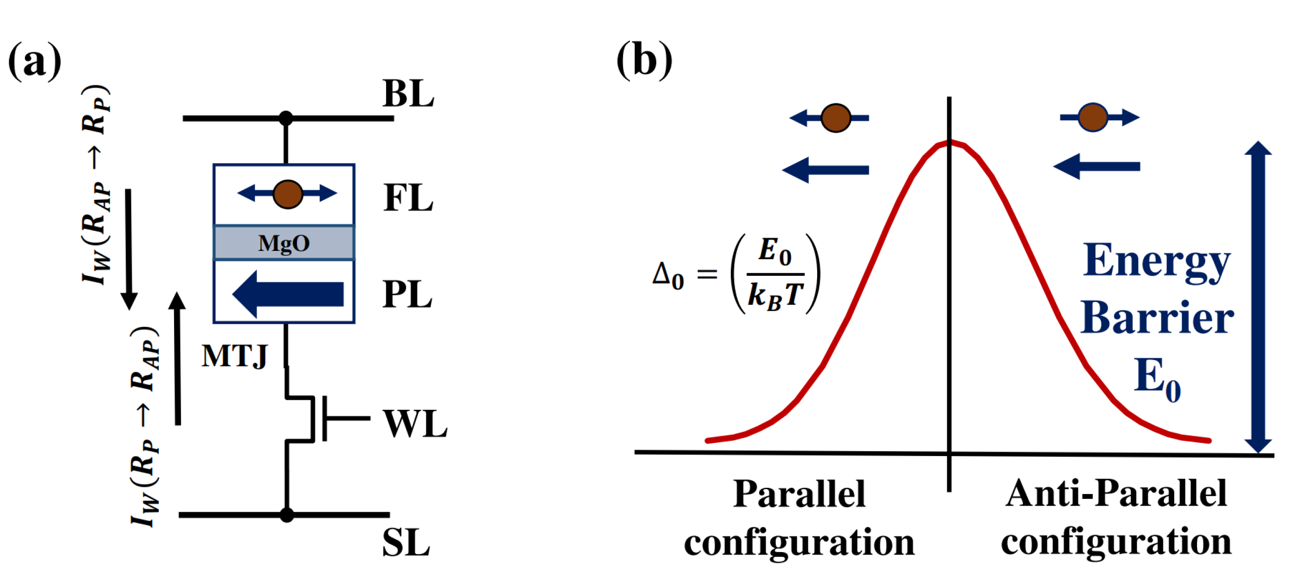
3.1. Basics of STTRAM
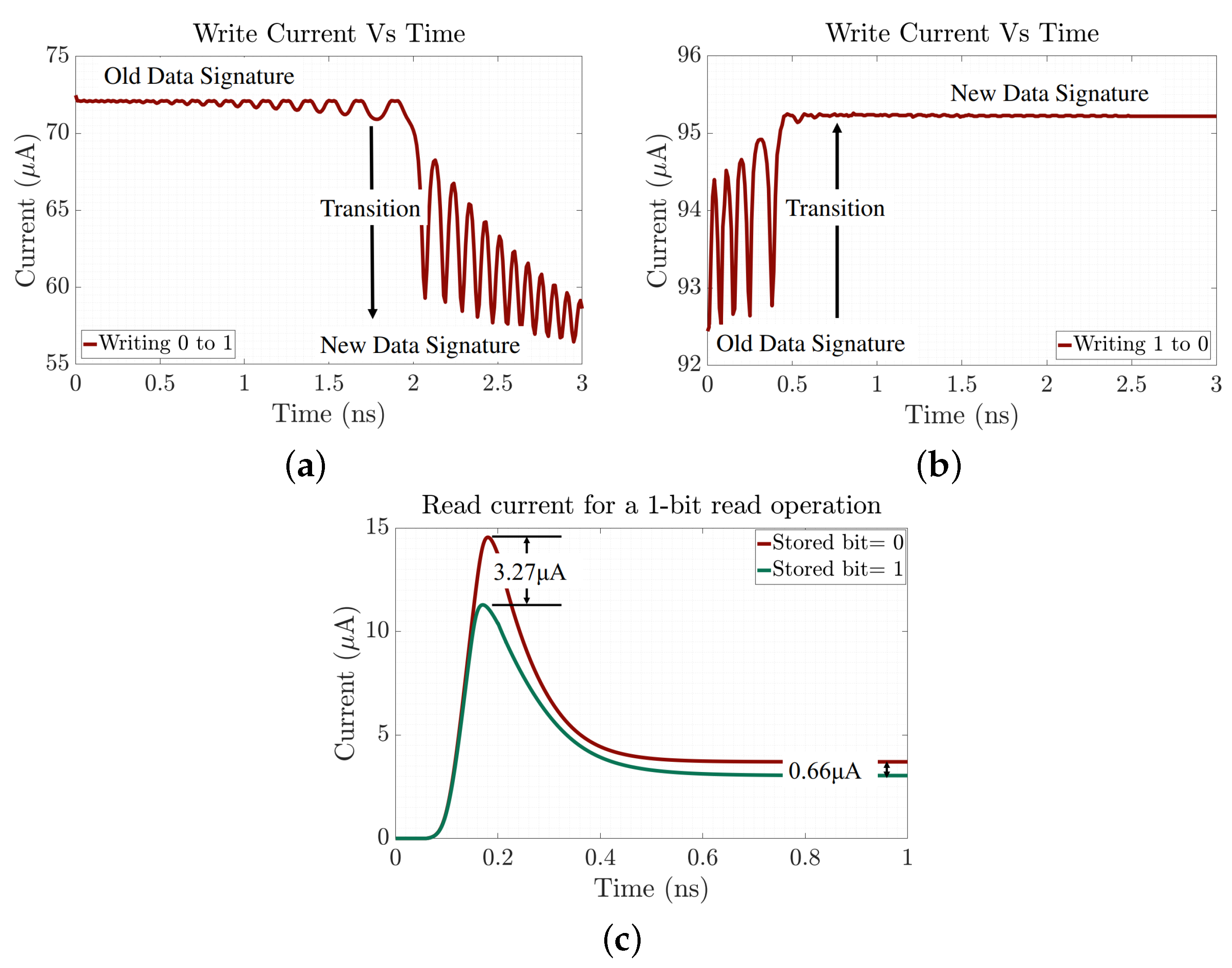
3.2. Asymmetric Write and Read Current
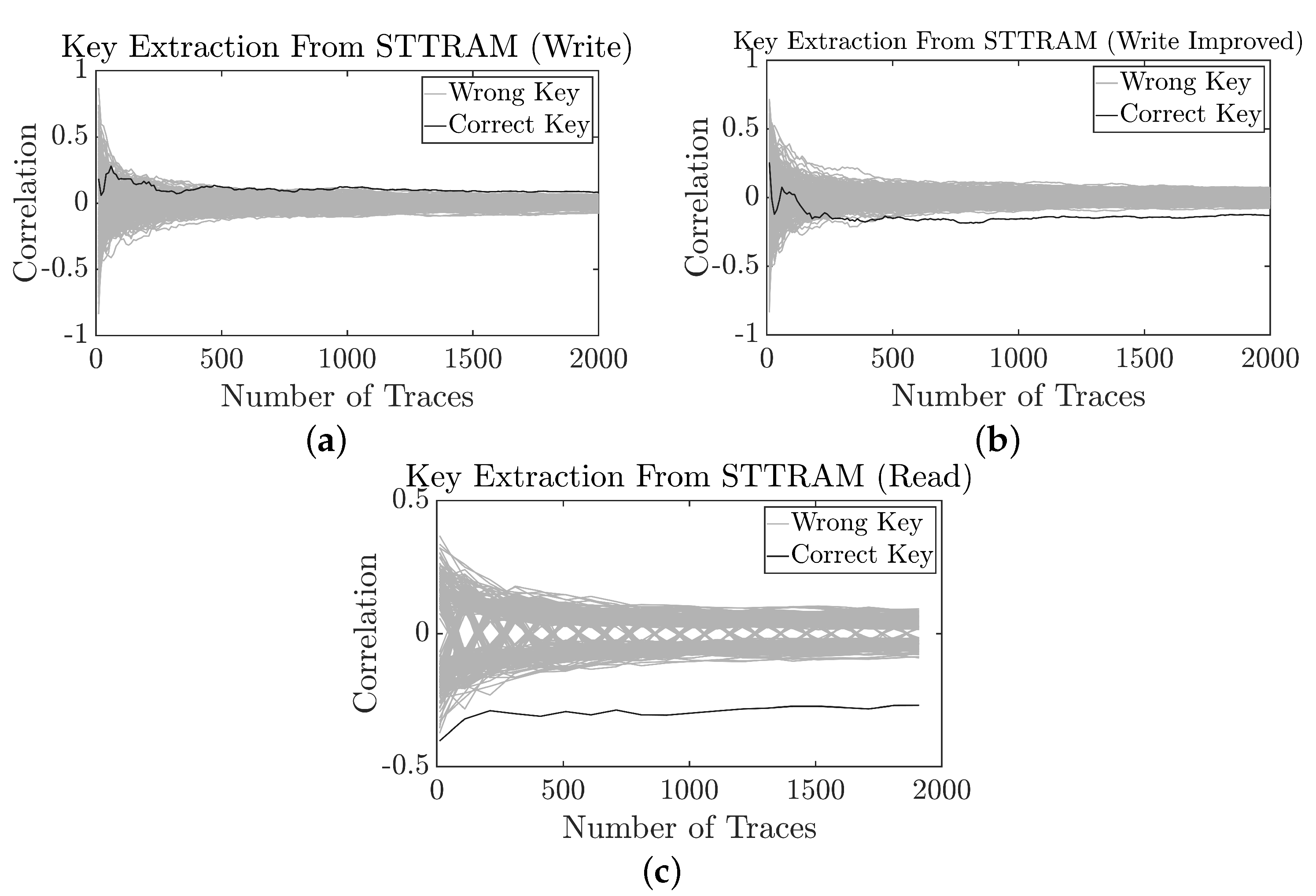
3.3. SCA on STTRAM Write Operation
3.4. SCA on STTRAM Read Operation
4. Case Study: MRAM
4.1. Basics of MRAM
4.2. Experimental Setup
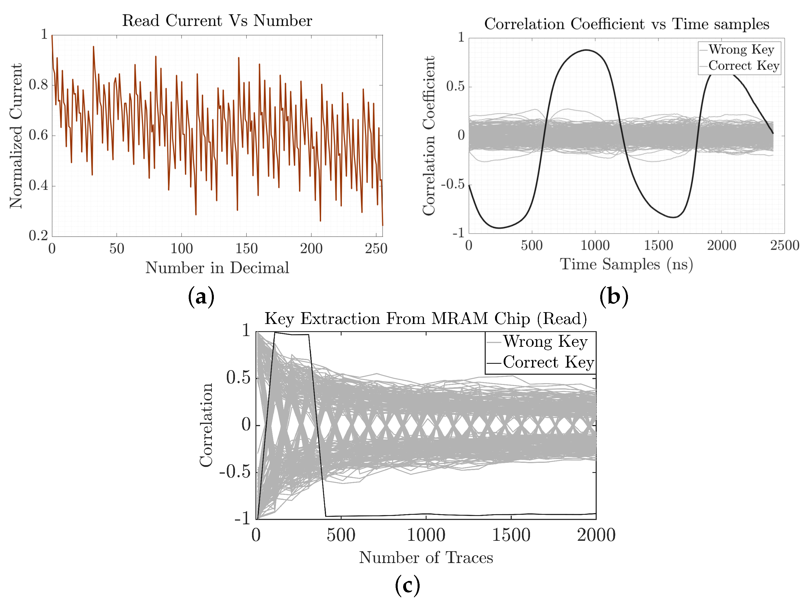
4.3. SCA on MRAM Write Operation
4.4. SCA on MRAM Read Operation
5. Case Study: RRAM
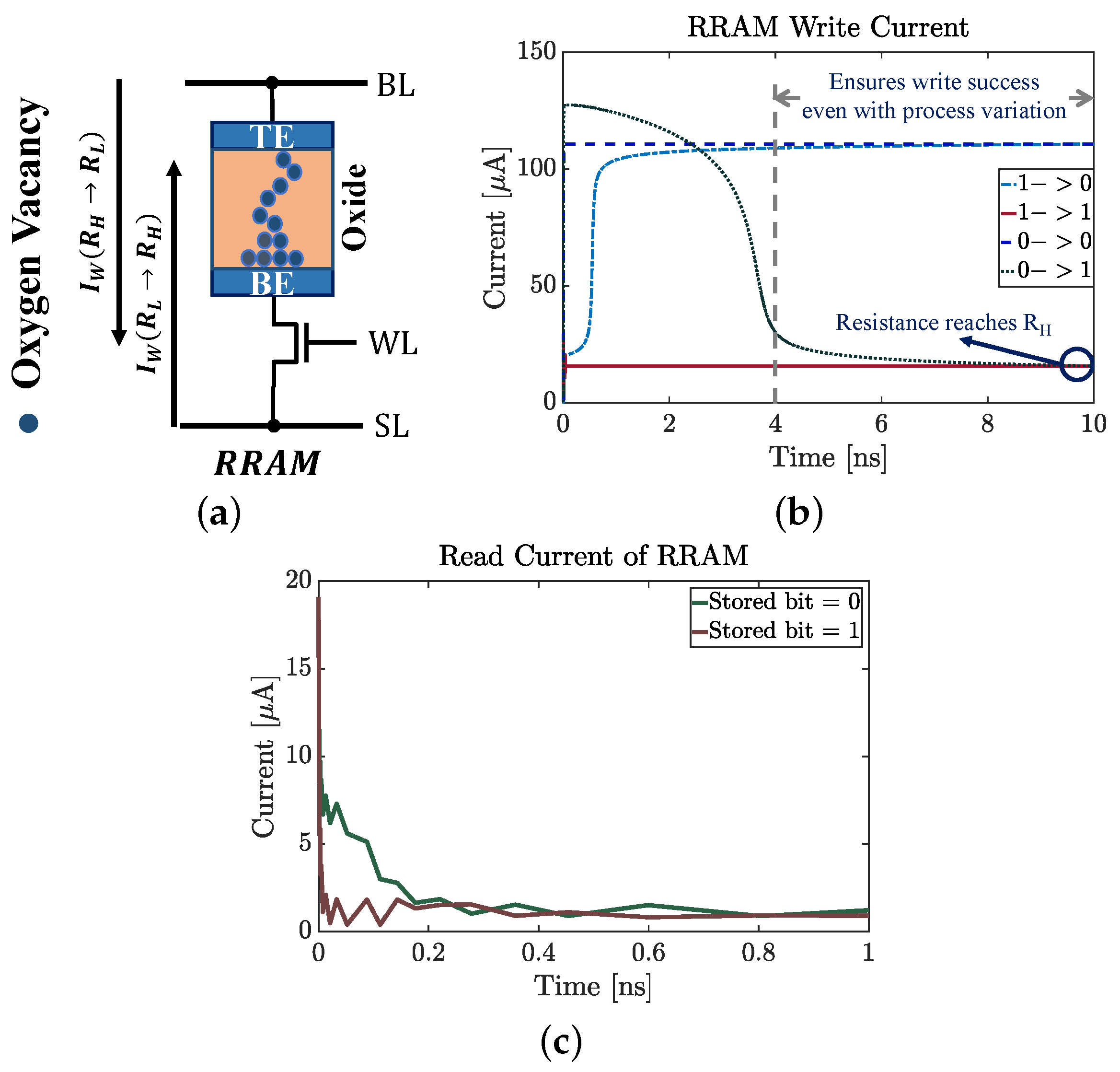
5.1. Basics of RRAM
5.2. Asymmetric Read/Write Current
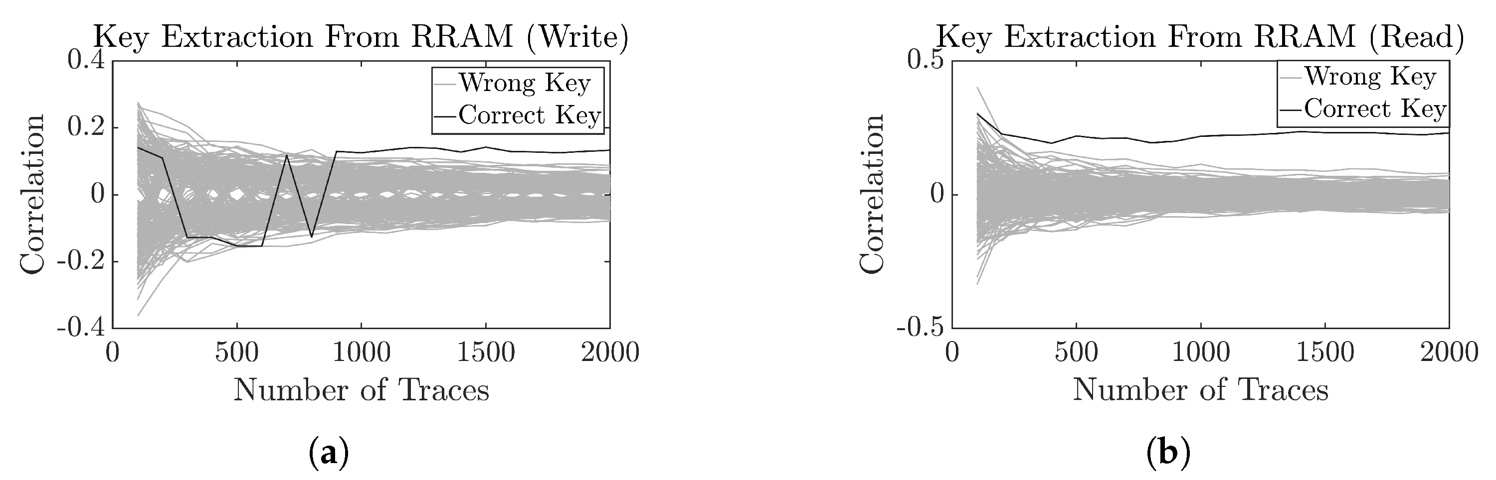
5.3. SCA on RRAM Write Operation
5.4. SCA on RRAM Read Operation
6. Case Study: PCM
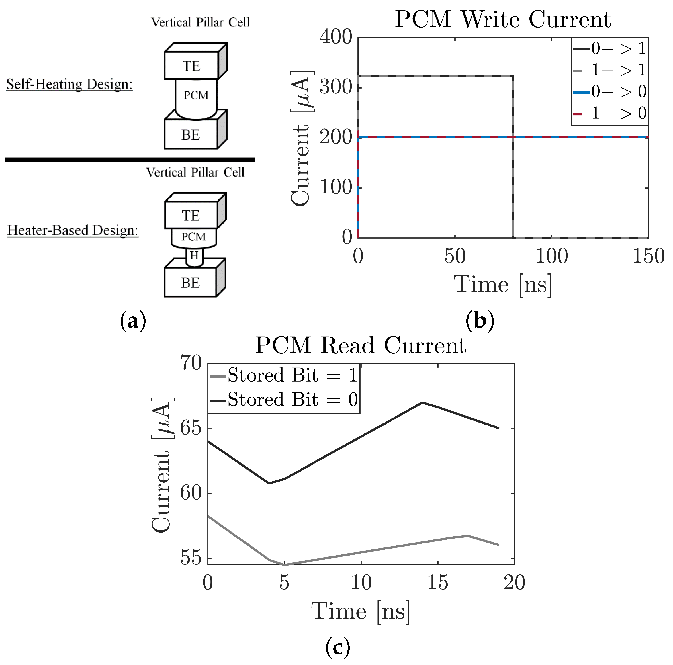
6.1. Basics of PCM
6.2. Asymmetric Read and Write Current
6.3. SCA on PCM Write Operation
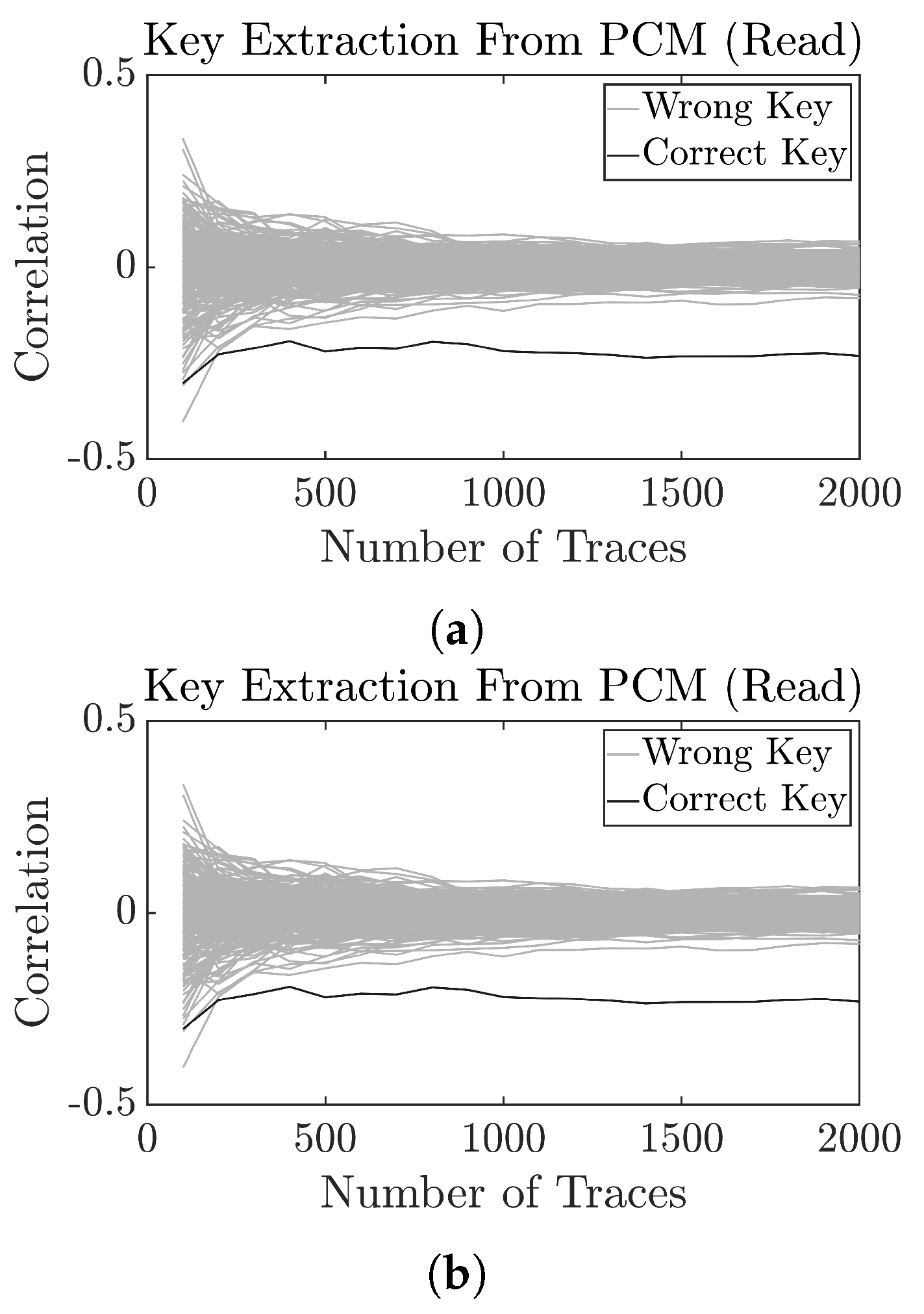
6.4. SCA on PCM Read Operation
6.5. Comparative Analysis of NVM Vulnerability to SCA
7. Analysis of Encoding as a Mitigation Technique
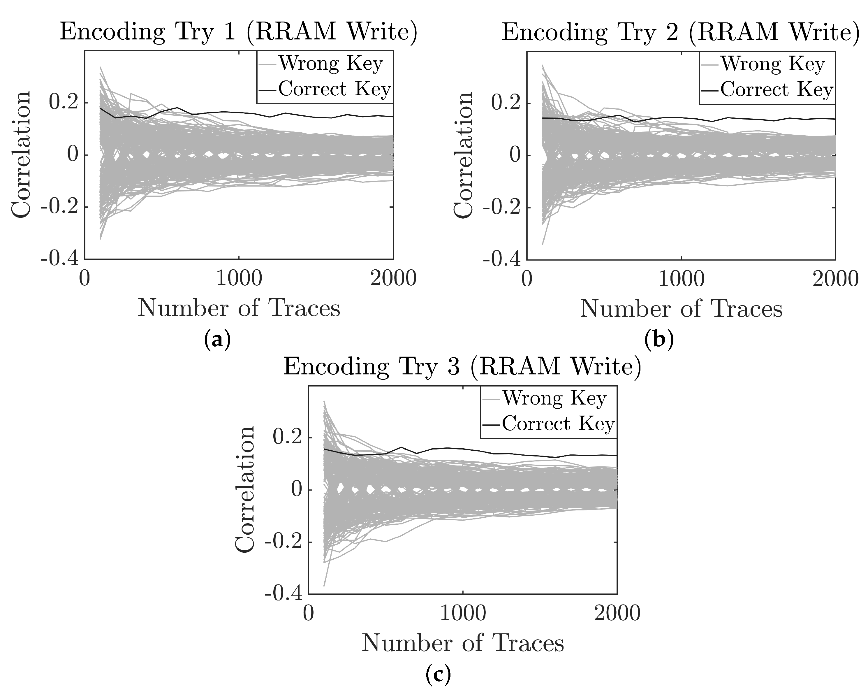
- Write Encoding Try 1: Out of 128-bit write data, first MSB 8 bits are encoded with reverse polarity. This means that for those 8 bits, high resistance state is considered as data ‘0’ and low resistance state is considered as data ‘1’. The key extraction result is shown in Figure 11a. It is evident that the attack is successful and the first byte of the key can be retrieved in roughly 800 traces.
- Write Encoding Try 2: Out of 128-bit write data, first MSB 16 bits are encoded with reverse polarity. Figure 11b shows the corresponding successful attack result where the first byte of the key can be retrieved in roughly 950 traces.
- Write Encoding Try 3: Out of 128-bit write data, first MSB 32 bits are encoded with reverse polarity. The attack result is summarized in Figure 11c. The first byte of the key can be retrieved in roughly 600 traces.
- Write Encoding Try 4: Out of 128-bit write data, first MSB 64 bits are encoded with reverse polarity. Figure 12a shows that the first byte of the key can be retrieved in roughly 600 traces.
- Read Encoding Try 1: Out of 128-bit read data, first MSB 32 bits are encoded with reverse polarity. Figure 12b shows that the first byte of the key can be retrieved in roughly 350 traces.
- Read Encoding Try 2: Out of 128-bit read data, first MSB 64 bits are encoded with reverse polarity. The attack result is summarized in Figure 12c. We note that the first byte of the key can be retrieved in roughly 200 traces.
8. Discussion
8.1. Assumptions Used in This Work
8.2. Considerations for Improving SCA Efficiency
8.3. Considerations for SCA Resiliency
9. Conclusions
Author Contributions
Funding
Data Availability Statement
Conflicts of Interest
References
- Worledge, D.C.; Hu, G.; Trouilloud, P.L.; Abraham, D.W.; Brown, S.; Gaidis, M.C.; Nowak, J.; O’Sullivan, E.J.; Robertazzi, R.P.; Sun, J.Z.; et al. Switching distributions and write reliability of perpendicular spin torque MRAM. In Proceedings of the 2010 International Electron Devices Meeting, San Francisco, CA, USA, 6–8 December 2010; pp. 12.5.1–12.5.4. [Google Scholar] [CrossRef]
- Lee, T.Y.; Yamane, K.; Hau, L.Y.; Chao, R.; Chung, N.L.; Naik, V.B.; Sivabalan, K.; Kwon, J.; Lim, J.H.; Neo, W.P.; et al. Magnetic Immunity Guideline for Embedded MRAM Reliability to Realize Mass Production. In Proceedings of the 2020 IEEE International Reliability Physics Symposium (IRPS), Dallas, TX, USA, 28 April–30 May 2020. [Google Scholar] [CrossRef]
- Nigam, A.; Smullen, C.W.; Mohan, V.; Chen, E.; Gurumurthi, S.; Stan, M.R. Delivering on the promise of universal memory for spin-transfer torque RAM (STT-RAM). In Proceedings of the IEEE/ACM International Symposium on Low Power Electronics and Design, Fukuoka, Japan, 1–3 August 2011; pp. 121–126. [Google Scholar] [CrossRef]
- Baranwal, M.; Chugh, U.; Dalal, S.; Agarwal, S.; Kapoor, H.K. DAMUS: Dynamic Allocation based on Write Frequency in MUlti-Retention STT-RAM based Last Level Caches. In Proceedings of the 2021 22nd International Symposium on Quality Electronic Design (ISQED), Santa Clara, CA, USA, 7–9 April 2021. [Google Scholar] [CrossRef]
- Kuan, K.; Adegbija, T. A Study of Runtime Adaptive Prefetching for STTRAM L1 Caches. In Proceedings of the 2020 IEEE 38th International Conference on Computer Design (ICCD), Hartford, CT, USA, 18–21 October 2020. [Google Scholar] [CrossRef]
- Pirovano, A.; Lacaita, A.L.; Pellizzer, F.; Kostylev, S.A.; Benvenuti, A.; Bez, R. Low-field amorphous state resistance and threshold voltage drift in chalcogenide materials. IEEE Trans. Electron Devices 2004, 51, 714–719. [Google Scholar] [CrossRef]
- Gong, H.; Ume, R.; Tokranov, V.; Yakimov, M.; Sadana, D.; Brew, K.; Cohen, G.; Schujman, S.; Beckmann, K.; Cady, N.; et al. Bilayer Ga-Sb Phase Change Memory with Intermediate Resistance State. In Proceedings of the 2021 Device Research Conference (DRC), Santa Barbara, CA, USA, 20–23 June 2021. [Google Scholar] [CrossRef]
- Wu, Y.; Yu, S.; Guan, X.; Wong, H.S.P. Recent progress of resistive switching random access memory (RRAM). In Proceedings of the 2012 IEEE Silicon Nanoelectronics Workshop (SNW), Honolulu, HI, USA, 10–11 June 2012; pp. 1–4. [Google Scholar] [CrossRef]
- Xu, M.; Gao, B.; Xu, F.; Wu, W.; Tang, J.; Chen, J.; Qian, H. A Compact Model of Analog RRAM Considering Temperature Coefficient for Neural Network Evaluation. In Proceedings of the 2021 5th IEEE Electron Devices Technology & Manufacturing Conference (EDTM), Chengdu, China, 8–11 April 2021. [Google Scholar] [CrossRef]
- Chen, A. A review of emerging non-volatile memory (NVM) technologies and applications. Solid-State Electron. 2016, 125, 25–38. [Google Scholar] [CrossRef]
- Xue, C.J.; Sun, G.; Zhang, Y.; Yang, J.J.; Chen, Y.; Li, H. Emerging non-volatile memories: Opportunities and challenges. In Proceedings of the 2011 Proceedings of the Ninth IEEE/ACM/IFIP International Conference on Hardware/Software Codesign and System Synthesis (CODES+ISSS), Taipei, Taiwan, 9–14 October 2011; pp. 325–334. [Google Scholar] [CrossRef]
- De, A.; Khan, M.N.I.; Park, J.; Ghosh, S. Replacing eFlash with STTRAM in IoTs: Security Challenges and Solutions. J. Hardw. Syst. Secur. 2017, 1, 328–339. [Google Scholar] [CrossRef]
- Intel Optane Memory Series. 2015. Available online: https://ark.intel.com/products/97544/Intel-Optane-Memory-Series-16GB-M_2-80mm-PCIe-3_0-20nm-3D-Xpoint (accessed on 3 May 2018).
- Ghosh, S.; Khan, M.N.I.; De, A.; Jang, J.W. Security and privacy threats to on-chip Non-Volatile Memories and countermeasures. In Proceedings of the 2016 IEEE/ACM International Conference on Computer-Aided Design (ICCAD), Austin, TX, USA, 7–10 November 2016; pp. 1–6. [Google Scholar] [CrossRef] [Green Version]
- Khan, M.N.I.; Ghosh, S. Fault Injection Attacks on Emerging Non-volatile Memory and Countermeasures. In Proceedings of the 7th International Workshop on Hardware and Architectural Support for Security and Privacy, HASP ’18, Los Angeles, CA, USA, 2 June 2018; ACM: New York, NY, USA, 2018; pp. 10:1–10:8. [Google Scholar] [CrossRef]
- Diao, Z.; Li, Z.; Wang, S.; Ding, Y.; Panchula, A.; Chen, E.; Wang, L.C.; Huai, Y. Spin-transfer torque switching in magnetic tunnel junctions and spin-transfer torque random access memory. J. Phys. Condens. Matter 2007, 19, 165209. [Google Scholar] [CrossRef]
- Shamsi, K.; Jin, Y. Security of emerging non-volatile memories: Attacks and defenses. In Proceedings of the 2016 IEEE 34th VLSI Test Symposium (VTS), Las Vegas, NV, USA, 25–27 April 2016; pp. 1–4. [Google Scholar] [CrossRef]
- Sugawara, T.; Suzuki, D.; Saeki, M.; Shiozaki, M.; Fujino, T. On measurable side-channel leaks inside ASIC design primitives. In International Workshop on Cryptographic Hardware and Embedded Systems; Springer: Berlin/Heidelberg, Germany, 2013; pp. 159–178. [Google Scholar]
- Shan, W.; Chen, X.; Li, B.; Cao, P.; Li, J.; Gao, G.; Shi, L. Evaluation of Correlation Power Analysis Resistance and Its Application on Asymmetric Mask Protected Data Encryption Standard Hardware. IEEE Trans. Instrum. Meas. 2013, 62, 2716–2724. [Google Scholar] [CrossRef]
- Lazzaroni, M.; Piuri, V.; Maziero, C. Computer security aspects in industrial instrumentation and measurements. In Proceedings of the 2010 IEEE Instrumentation Measurement Technology Conference Proceedings, Austin, TX, USA, 3–6 May 2010; pp. 1216–1221. [Google Scholar] [CrossRef]
- Bilski, P.; Winiecki, W.; Adamski, T. Implementation of symmetric cryptography in embedded systems for secure measurement systems. In Proceedings of the 2011 IEEE International Instrumentation and Measurement Technology Conference, Hangzhou, China, 10–12 May 2011; pp. 1–6. [Google Scholar] [CrossRef]
- Wu, J.; Shi, Y.; Choi, M. Measurement and Evaluation of Power Analysis Attacks on Asynchronous S-Box. IEEE Trans. Instrum. Meas. 2012, 61, 2765–2775. [Google Scholar] [CrossRef]
- Fong, X.; Choday, S.H.; Roy, K. Design and optimization of spin-transfer torque mrams. In More than Moore Technologies for Next Generation Computer Design; Springer: Berlin/Heidelberg, Germany, 2015; pp. 49–72. [Google Scholar]
- Konstantakos, V.; Kosmatopoulos, K.; Nikolaidis, S.; Laopoulos, T. Measurement of Power Consumption in Digital Systems. IEEE Trans. Instrum. Meas. 2006, 55, 1662–1670. [Google Scholar] [CrossRef]
- Khan, M.N.I.; Bhasin, S.; Yuan, A.; Chattopadhyay, A.; Ghosh, S. Side-Channel Attack on STTRAM Based Cache for Cryptographic Application. In Proceedings of the 2017 IEEE International Conference on Computer Design (ICCD), Boston, MA, USA, 5–8 November 2017; pp. 33–40. [Google Scholar] [CrossRef]
- Lee, D.; Gupta, S.K.; Roy, K. High-performance low-energy STT MRAM based on balanced write scheme. In Proceedings of the 2012 ACM/IEEE International Symposium on Low Power Electronics and Design, Redondo Beach, CA, USA, 30 July–1 August 2012; ACM: New York, NY, USA, 2012; pp. 9–14. [Google Scholar]
- Chakraborty, A.; Mondal, A.; Srivastava, A. Correlation Power Analysis Attack against STT-MRAM Based Cyptosystems. IACR Cryptol. ePrint Arch. 2017, 2017, 413. [Google Scholar]
- Srikant, S. All Spin Logic: Modeling Multi-Magnet Networks Interacting via Snin Currents. Ph.D. Dissertation, Purdue University, West Lafayette, IN, USA, 2012. [Google Scholar]
- Kocher, P.; Jaffe, J.; Jun, B. Differential power analysis. In Annual International Cryptology Conference; Springer: Berlin/Heidelberg, Germany, 1999; pp. 388–397. [Google Scholar]
- Bernstein, D.J. Cache-Timing Attacks on AES. 2005. Available online: https://cr.yp.to/antiforgery/cachetiming-20050414.pdf (accessed on 15 September 2021).
- Gandolfi, K.; Mourtel, C.; Olivier, F. Electromagnetic analysis: Concrete results. In International Workshop on Cryptographic Hardware and Embedded Systems; Springer: Berlin/Heidelberg, Germany, 2001; pp. 251–261. [Google Scholar]
- Brier, E.; Clavier, C.; Olivier, F. Correlation power analysis with a leakage model. In International Workshop on Cryptographic Hardware and Embedded Systems; Springer: Berlin/Heidelberg, Germany, 2004; pp. 16–29. [Google Scholar]
- Rauzy, P.; Guilley, S.; Najm, Z. Formally proved security of assembly code against power analysis. J. Cryptogr. Eng. 2016, 6, 201–216. [Google Scholar] [CrossRef] [Green Version]
- MR4A08B Datasheet. Available online: https://www.everspin.com/getdatasheet/MR4A08B (accessed on 13 March 2019).
- Basys 3 FPGA Board Reference Manual. Available online: https://reference.digilentinc.com/_media/basys3:basys3_rm.pdf (accessed on 13 March 2019).
- Artix-7 FPGAs Data Sheet. Available online: https://www.xilinx.com/support/documentation/data_sheets/ds181_Artix_7_Data_Sheet.pdf (accessed on 13 March 2019).
- Infiniium S-Series, The Standard for Superior Measurements Data Sheet. Available online: https://literature.cdn.keysight.com/litweb/pdf/5991-3904EN.pdf?id=2447379 (accessed on 13 March 2019).
- Chen, P.Y.; Yu, S. Compact Modeling of RRAM Devices and Its Applications in 1T1R and 1S1R Array Design. IEEE Trans. Electron Devices 2015, 62, 4022–4028. [Google Scholar] [CrossRef]
- Boniardi, M.; Redaelli, A.; Cupeta, C.; Pellizzer, F.; Crespi, L.; D’Arrigo, G.; Lacaita, A.L.; Servalli, G. Optimization metrics for Phase Change Memory (PCM) cell architectures. In Proceedings of the 2014 IEEE International Electron Devices Meeting, San Francisco, CA, USA, 15–17 December 2014; pp. 29.1.1–29.1.4. [Google Scholar] [CrossRef]
- Russo, U.; Ielmini, D.; Redaelli, A.; Lacaita, A.L. Modeling of Programming and Read Performance in Phase-Change Memories—Part I: Cell Optimization and Scaling. IEEE Trans. Electron Devices 2008, 55, 506–514. [Google Scholar] [CrossRef]
- Servalli, G. A 45nm generation Phase Change Memory technology. In Proceedings of the 2009 IEEE International Electron Devices Meeting (IEDM), Baltimore, MD, USA, 7–9 December 2009; pp. 1–4. [Google Scholar] [CrossRef]
- Pellizzer, F.; Pirovano, A.; Ottogalli, F.; Magistretti, M.; Scaravaggi, M.; Zuliani, P.; Tosi, M.; Benvenuti, A.; Besana, P.; Cadeo, S.; et al. Novel /spl mu/trench phase-change memory cell for embedded and stand-alone non-volatile memory applications. In Proceedings of the Digest of Technical Papers. 2004 Symposium on VLSI Technology, 2004, Honolulu, HI, USA, 15–17 June 2004; pp. 18–19. [Google Scholar] [CrossRef]
- Kim, E.T.; Lee, J.Y.; Kim, Y.T. Investigation of electrical characteristics of the In3Sb1Te2 ternary alloy for application in Phase Change Memory. Phys. Status Solidi RRL-Rapid Res. Lett. 2009, 3, 103–105. [Google Scholar] [CrossRef]
- Xu, Z.; Sutaria, K.B.; Yang, C.; Chakrabarti, C.; Cao, Y. Hierarchical modeling of Phase Change memory for reliable design. In Proceedings of the 2012 IEEE 30th International Conference on Computer Design (ICCD), Montreal, QC, Canada, 30 September–3 October 2012; pp. 115–120. [Google Scholar] [CrossRef]
- Maghrebi, H.; Servant, V.; Bringer, J. There is wisdom in harnessing the strengths of your enemy: Customized encoding to thwart side-channel attacks. In International Conference on Fast Software Encryption; Springer: Berlin/Heidelberg, Germany, 2016; pp. 223–243. [Google Scholar]
- Bhasin, S.; Jap, D.; Peyrin, T. Practical Evaluation of FSE 2016 Customized Encoding Countermeasure. IACR Trans. Symmetric Cryptol. 2017, 2017, 108–129. [Google Scholar] [CrossRef]
- Kar, M.; Singh, A.; Mathew, S.; Rajan, A.; De, V.; Mukhopadhyay, S. Exploiting fully integrated inductive voltage regulators to improve side channel resistance of encryption engines. In Proceedings of the 2016 International Symposium on Low Power Electronics and Design, San Francisco, CA, USA, 8–10 August 2016; ACM: New York, NY, USA, 2016; pp. 130–135. [Google Scholar]
- Nagarajan, K.; Ahmed, F.U.; Khan, M.N.I.; De, A.; Chowdhury, M.H.; Ghosh, S. SecNVM: Power Side-Channel Elimination Using On-Chip Capacitors for Highly Secure Emerging NVM. IEEE Trans. Very Large Scale Integr. VLSI Syst. 2021, 29, 1518–1528. [Google Scholar] [CrossRef]
- Ahmed, F.U.; Sandhie, Z.T.; Chowdhury, M.H. An Implementation of External Capacitor-less Low-DropOut Voltage Regulator in 45 nm Technology with Output Voltage Ranging from 0.4 V–1.2 V. In Proceedings of the 2020 IEEE 38th International Conference on Computer Design (ICCD), Hartford, CT, USA, 18–21 October 2020; pp. 453–456. [Google Scholar] [CrossRef]


| Parameter | Value |
|---|---|
| Access transistor (nMOS) (W/L) | 100 nm/30 nm |
| MTJ FL volume | 1.04 × 10⁻¹⁷ cm3 |
| MTJ anisotropy (uniaxial), Ku | 150,150 erg/cc |
| Magnetization saturation, Ms | 790 Oe |
| MTJ anisotropic magnetic field, Hk | 380 Oe |
| MTJ Thermal barrier, Δ | 37.99 |
| Tunnel magnetoresistance, TMR | 2 |
| Write/read latency | 3 ns/1 ns |
| nMOS/pMOS width ratio (read circuit) | 1/6 |
| Parameter | Value |
|---|---|
| Capacity | 16 Mbit |
| Write/Read latency | 35 ns |
| Data/Address bus length | 8/21 |
| 3.3 V | |
| Data retention time | >20 years |
| AC standby current | 9–14 mA |
| AC active current (read) | 60–68 mA |
| AC Active Current (write) | 152–180 mA |
| Output enable access time | 15 ns |
| Parameter | Value |
|---|---|
| Access Transistor W/L/VT | 195 nm/65 nm/0.423 V |
| RRAM Gap for RL/RH | 0.53 nm/1.368 nm |
| Unit Cell Size | 12 F2 |
| System Clock Frequency/Vdd | 2 GHz/2.2 V |
| Read/Write Latency | 0.5 ns (1 cycle)/10 ns (20 cycle) |
| Parameter | Value |
|---|---|
| Access Transistor W/L/VT | 195 nm/65 nm/0.423 V |
| Bottom Contact Width, CW | 28 nm |
| GST thickness | 49 nm |
| RSET/RRESET/RWRITE | 9 kΩ/3.6 MΩ/1 kΩ |
| Read/Write Latency | 20 ns (40 cycle)/150 ns (300 cycle) |
| NVM | MTD |
|---|---|
| STTRAM (write) | 300 |
| STTRAM (read) | 40 |
| MRAM (read) | 15 |
| RRAM (write) | 900 |
| RRAM (read) | 200 |
| PCM (write) | 200 |
| PCM (read) | 200 |
Publisher’s Note: MDPI stays neutral with regard to jurisdictional claims in published maps and institutional affiliations. |
© 2021 by the authors. Licensee MDPI, Basel, Switzerland. This article is an open access article distributed under the terms and conditions of the Creative Commons Attribution (CC BY) license (https://creativecommons.org/licenses/by/4.0/).
Share and Cite
Khan, M.N.I.; Bhasin, S.; Liu, B.; Yuan, A.; Chattopadhyay, A.; Ghosh, S. Comprehensive Study of Side-Channel Attack on Emerging Non-Volatile Memories. J. Low Power Electron. Appl. 2021, 11, 38. https://0-doi-org.brum.beds.ac.uk/10.3390/jlpea11040038
Khan MNI, Bhasin S, Liu B, Yuan A, Chattopadhyay A, Ghosh S. Comprehensive Study of Side-Channel Attack on Emerging Non-Volatile Memories. Journal of Low Power Electronics and Applications. 2021; 11(4):38. https://0-doi-org.brum.beds.ac.uk/10.3390/jlpea11040038
Chicago/Turabian StyleKhan, Mohammad Nasim Imtiaz, Shivam Bhasin, Bo Liu, Alex Yuan, Anupam Chattopadhyay, and Swaroop Ghosh. 2021. "Comprehensive Study of Side-Channel Attack on Emerging Non-Volatile Memories" Journal of Low Power Electronics and Applications 11, no. 4: 38. https://0-doi-org.brum.beds.ac.uk/10.3390/jlpea11040038