Article

Mapping Transformation Enabled High-Performance and Low-Energy Memristor-Based DNNs

1
Department of Electrical and Computer Engineering, University of South Alabama, Mobile, AL 36688, USA
2
Department of Electrical and Computer Engineering, Northeastern University, Boston, MA 02115, USA
3
Department of Electrical and Computer Engineering, North Dakota State University, Fargo, ND 58105, USA
4
Department of Computer Science and Engineering, University of Connecticut, Storrs, CT 06269, USA
*
Author to whom correspondence should be addressed.
J. Low Power Electron. Appl. 2022, 12(1), 10; https://0-doi-org.brum.beds.ac.uk/10.3390/jlpea12010010
Submission received: 31 December 2021 / Revised: 28 January 2022 / Accepted: 7 February 2022 / Published: 10 February 2022
(This article belongs to the Special Issue Low Power AI)

Abstract

:
When deep neural network (DNN) is extensively utilized for edge AI (Artificial Intelligence), for example, the Internet of things (IoT) and autonomous vehicles, it makes CMOS (Complementary Metal Oxide Semiconductor)-based conventional computers suffer from overly large computing loads. Memristor-based devices are emerging as an option to conduct computing in memory for DNNs to make them faster, much more energy efficient, and accurate. Despite having excellent properties, the memristor-based DNNs are yet to be commercially available because of Stuck-At-Fault (SAF) defects. A Mapping Transformation (MT) method is proposed in this paper to mitigate Stuck-at-Fault (SAF) defects from memristor-based DNNs. First, the weight distribution for the VGG8 model with the CIFAR10 dataset is presented and analyzed. Then, the MT method is used for recovering inference accuracies at 0.1% to 50% SAFs with two typical cases, SA1 (Stuck-At-One): SA0 (Stuck-At-Zero) = 5:1 and 1:5, respectively. The experiment results show that the MT method can recover DNNs to their original inference accuracies (90%) when the ratio of SAFs is smaller than 2.5%. Moreover, even when the SAF is in the extreme condition of 50%, it is still highly efficient to recover the inference accuracy to 80% and 21%. What is more, the MT method acts as a regulator to avoid energy and latency overhead generated by SAFs. Finally, the immunity of the MT Method against non-linearity is investigated, and we conclude that the MT method can benefit accuracy, energy, and latency even with high non-linearity LTP = 4 and LTD = −4.

1. Introduction

Data generated from edge devices are increasing exponentially with the proliferation of the Internet of Things (IoT). To minimize the data exchange with the cloud, the edge devices handle more computational tasks than before, including processing, storage, caching, and load balancing [1]. Besides, the successful implementation of DNNs (Deep Neural Networks) on the edge device has further increased the computational complexity even more [2]. As edge devices are usually portable and used in real-time scenarios, the inference accuracy and latency as well as the energy consumption of the system are critical [3]. However, the conventional CMOS-based edge devices, such as a high-speed autonomous driving vehicle, face tremendous challenges to provide a quick and reliable response in nanoseconds or picoseconds. Moreover, this problem becomes difficult to solve because CMOS technology cannot continuously downscale to drive increment of the device speed [4,5]. Furthermore, the conventional CMOS-based edge devices struggle to adapt to data-centric applications (DNN) due to energy-hungry characteristics. Therefore, accuracy, latency, and energy consumption have become bottlenecks and restricted further development of edge AI (Artificial Intelligence) in IoT.
The emerging device—memristor—possesses great potential and can act as a rescuer from this deadlock. Years after Professor Chua’s postulation [6], Hewlett-Packard manufactured the first memristor device in 2008 and implemented crossbar junctions using a layer of platinum dioxide, followed by a monolayer film of switching molecules, and finally a layer of titanium [7]. Then, different materials and structures were proposed for memristors. For example, amorphous silicon (a- S i ) and silver ( A g ) have become popular memristive materials [8]. Later, p-type crystalline silicon was used as a bottom electrode along with A g : a- S i structure [9]. Chalcogenide-based devices were also fabricated, where A g 2 S e and A g were placed between Tungsten electrodes [10]. Likewise, titanium dioxide ( T i O 2 )- [11] and hafnium dioxide ( H f O 2 )-based [12] memristors also exhibited all the excellent traits that can be used in high-density memory and neuromorphic computing architecture. Apart from excellent characteristics like low computational complexity [13], low power consumption [14], fast switching speed [15], high endurance [16], excellent scalability [17], and CMOS-compatibility [18], memristor crossbar arrays can perform the in situ matrix-vector multiplication which is the most essential operation of the DNN algorithm [19], as shown in Figure 1. Unfortunately, due to the limitation of the immature fabrication, low manufacturing yield is common and induces faults for almost all the memristors [9,12]. These faults can be classified as hard faults or soft faults. If a memristor has soft faults, e.g., Read-One-Disturb (R1D) and Read-Zero-Disturb (R0D), it can be calibrated because the resistance/conductance is still changeable with an external stimulus. However, hard faults, especially Stuck-At-Faults (SAFs), cannot be removed, because memristors would always stick at high-resistance state (HRS) or low-resistance state (LRS) [12]. Consequently, weight values from mapped memristors and from DNN algorithms have a huge discrepancy which results in a significant accuracy degradation. What is more, SAFs change the weight distributions in memristor arrays and impacts overall energy consumption and system latency.
Some related research works have been implemented by researchers, but most of them aimed to alleviate the accuracy drop caused by SAFs. One method identifies the significant weights in the neural network first and then prevents them being mapped to the abnormal memristors [20,21]. Matrix transformation [22], stuck-at-fault tolerance [23], and fault-tolerant training with on-line fault detection [24] are some other SAF rescuing methods for restoring high inference accuracy in DNNs. Those methods are somewhat successful in restoring the original accuracy in certain extreme hardware failure cases like 20%. However, their shortcomings are as follows. (1) The above methods cause hardware overhead by adding additional large, complex control circuitry. (2) The above methods disregard reporting the energy for the inference, making practical implementation inefficient. Actually, it is obvious that the above methods will cause energy overhead. (3) The above methods increase system latency, degrading the performance of the memristor-based DNN in edge AI. (4) Most importantly, considering the sporadic nature of the SAF and the huge number of devices in industry (such as IoT applications), an individual optimization and custom design for each device is too time consuming and is not realistic.
Therefore, a new technique—Mapping Transformation (MT)—is proposed in this paper. This method creates a strong immunity against SAFs with the controllable energy consumption and latency. It does not aim to obtain the optimizing pattern for the individual device but covers any memristor-based product, and it can be largely used to improve the overall inference accuracy even as high as 50% in the SAFs case; therefore, it is especially appropriate for the industry. This paper makes the following contributions:
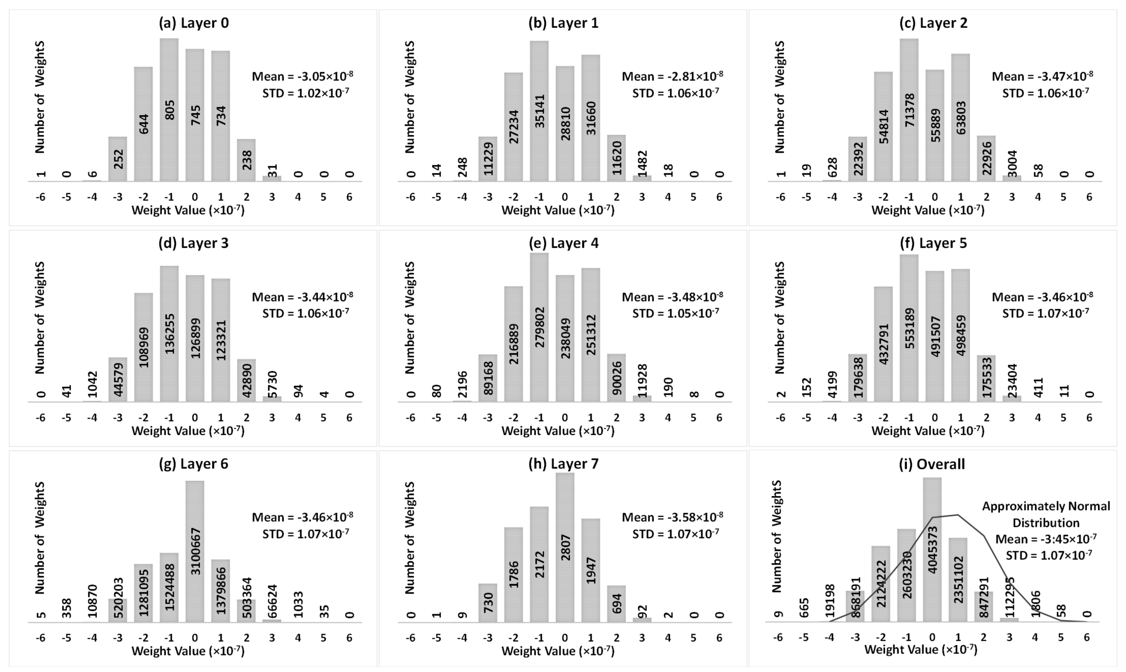
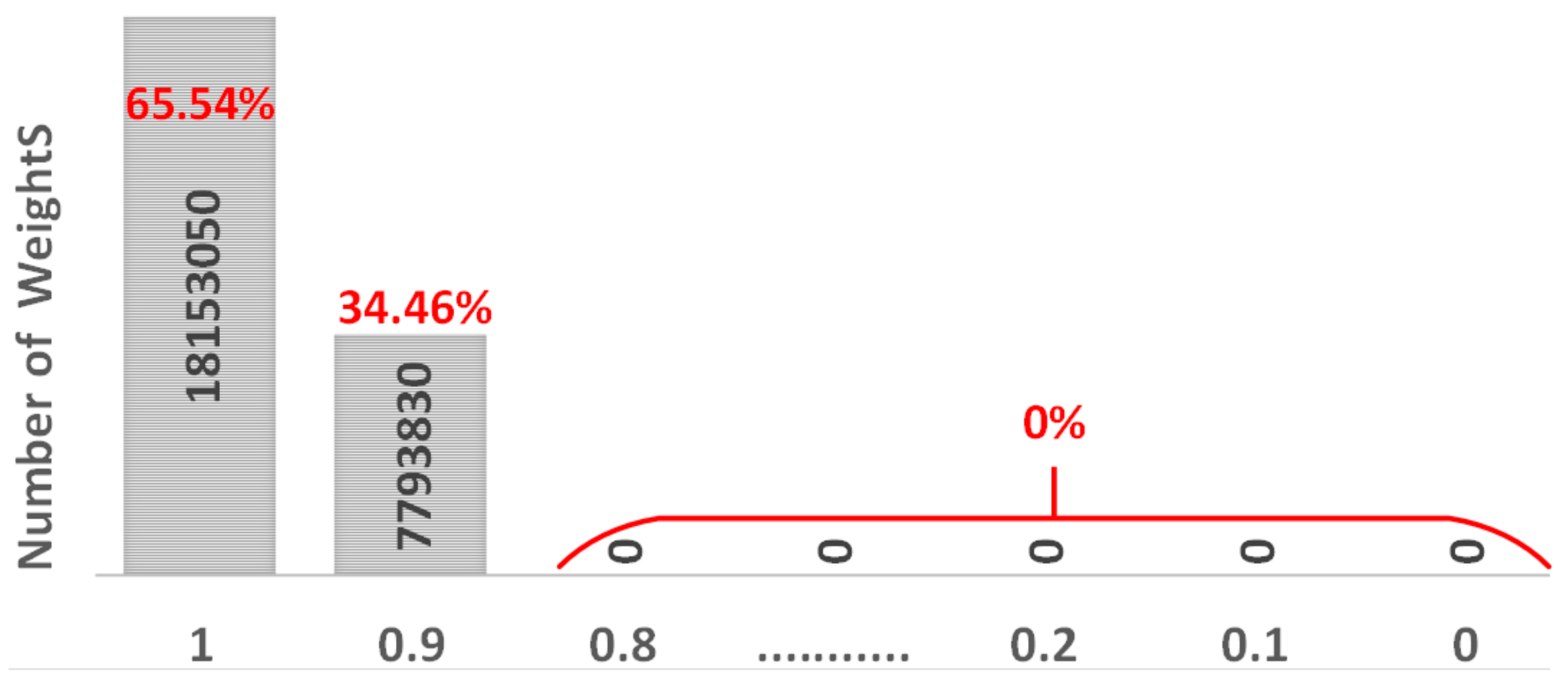
  • In order to investigate the inference accuracy drop in memristor-based DNNs due to SAFs, the weight distribution for the VGG8 model is presented and analyzed.
  • As the SAF defects are immensely random and vary from device to device, the accuracy drop of a DNN is listed for different SAF ratios from 0.1% to 50% with SA1:SA0 = 5:1 and 1:5, respectively.
  • A MT method is proposed to achieve outstanding accuracy recovery even in extremely high SAF cases.
  • The MT method for the accuracy improvement, energy saving, and latency reduction is validated on the VGG8 model with the CIFAR10 dataset.
  • It is also verified that even with the significant non-linear properties, the MT technology is still effective to recover the accuracy, save energy, and decrease latency in memristor-based DNNs under various SAF conditions.
  • Finally, the proposed MT method is compared with the state-of-the-art.

2. Methodology

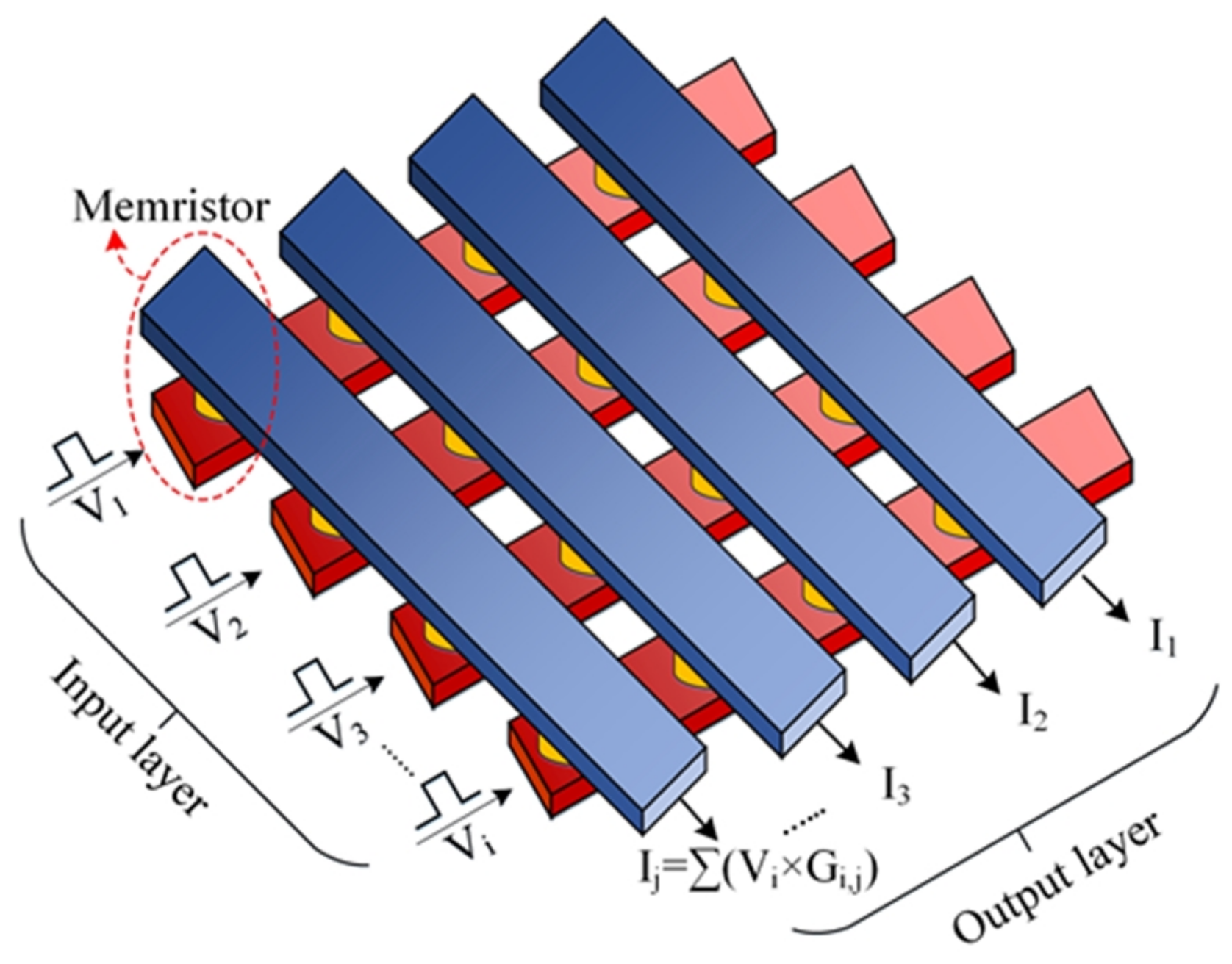
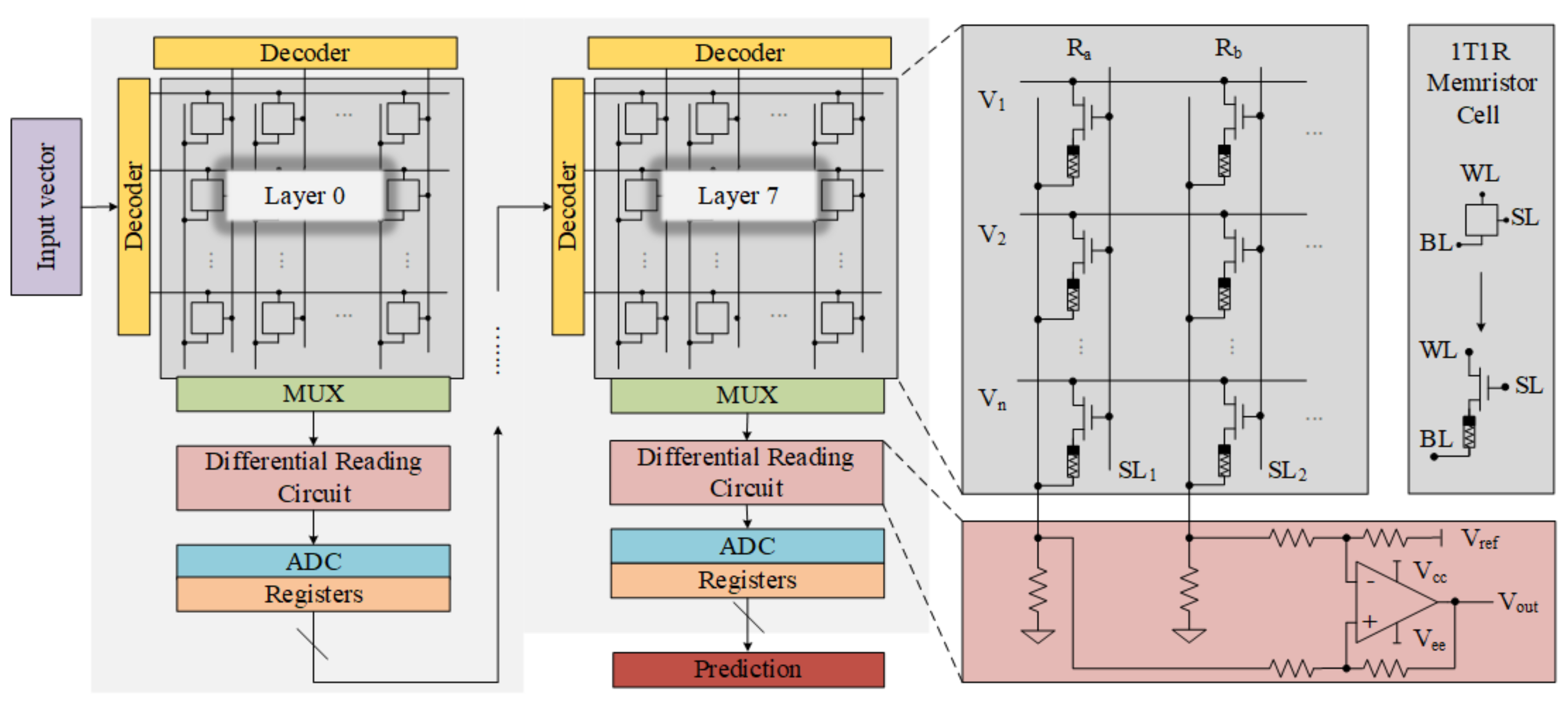
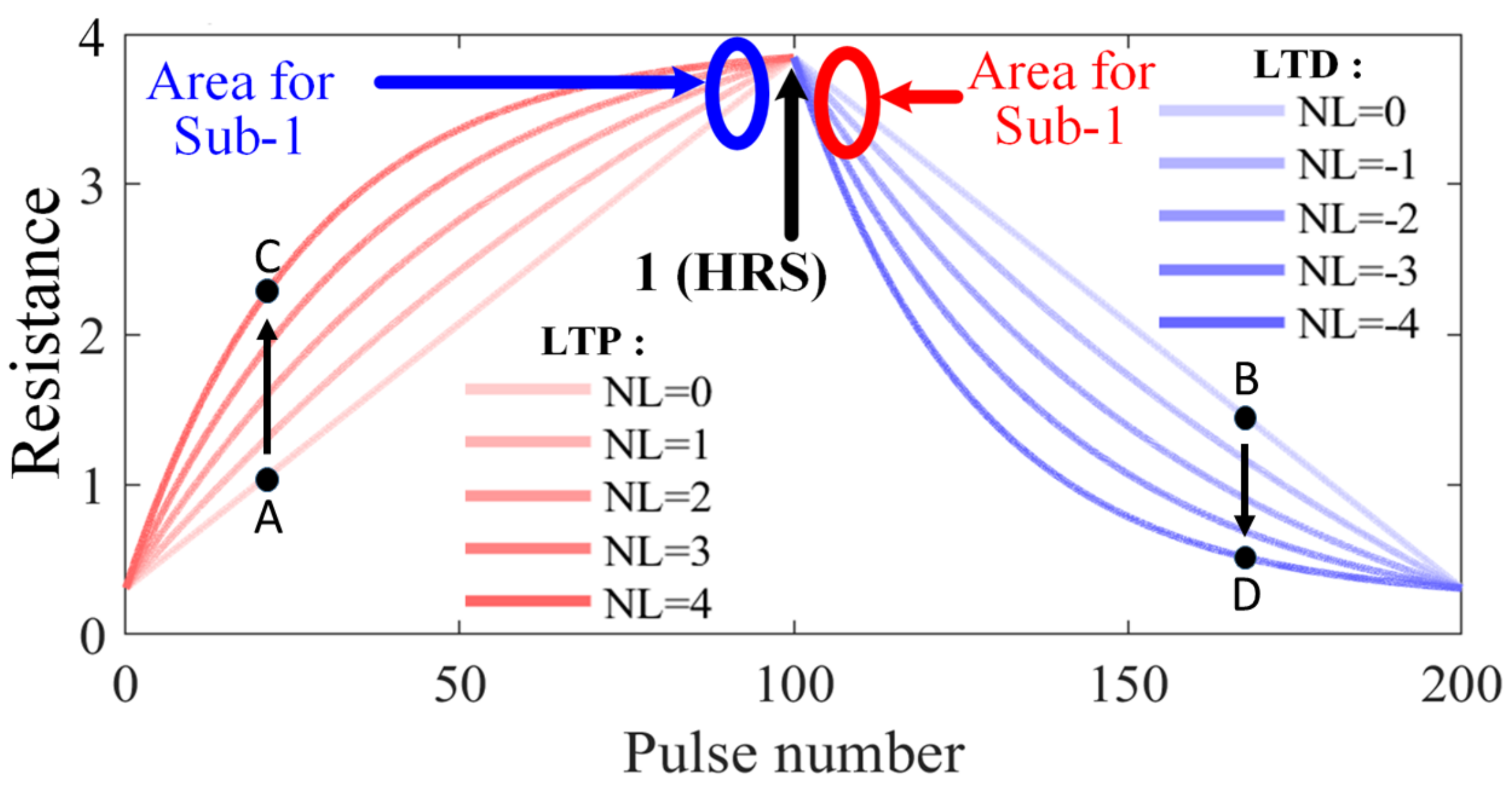
2.1. Stuck-At-Fault (SAF)

Memristors typically have a metal–insulator–metal (MIM) structure where the resistance of the device is determined by the insulation layer. When an external stimulus, such as positive or negative pulse, is applied to a memristor, a certain amount of current flexes through it and the resistance of the memristor changes between LRS to HRS. However, sometimes the resistance state becomes forever stuck at HRS or LRS and stays unchanged as a Stuck-At-Fault (SAF). This is because of the following: (1) During the complicated fabrication process, the memristor encounters some imperfections, such as oxide thickness fluctuation, line-edge roughness, and feature size shrinkage, making the memristor malfunction and become stuck at LRS/HRS [25]. (2) Memristors in a newly fabricated crossbar array must go through a forming process before performing the read/write operation. The highly sophisticated process continues as long as 100 usfor lowering the resistance to LRS from an extremely high initial resistance [12]. However, process variations and unstable taster voltages can result in overforming, causing the memrisor to become stuck at LRS [12]. (3) The memristor array structure, as shown in Figure 2, indicates that each memristor connects Word Line (WL), Bit Line (BL), and Select Line (SL) to perform the read/write operation. However, sometimes the broken WL or permanent open switch makes the memristor inaccessible for those operations. No matter what the actual resistance state is, the broken WL will always cause the read circuit to make a mistake as being HRS. Therefore, SAFs can be classified into Stuck-At-Zero (SA0) and Stuck-At-One (SA1) fault. SAFs would significantly degrade the inference accuracy of the memristor-based DNNs, especially when SAFs have high ratio in memristor arrays. Unfortunately, it is reported that a 4Mb Hafnium Dioxide ( H f O 2 )-based memristor array shows SA1 and SA0 of 9.04% and 1.75%, respectively [12]. In another worst-case scenario, overforming causes 60% of cells in memristor arrays to suffer from SA0 [12]. Most important, the defected cells disturb resistances of cells in memristor arrays, and thus the energy overhead is obviously to be generated. This phenomenon can be interpreted by the following equation [26].
E cell = 1 R V R 2 N T P U L S E
In Equation (1), R is the resistance of a memristor. V W is the reading voltage. N is the number of applied pulses while reading a certain weight, and T P U L S E is the pulse width. The total energy consumption can be estimated as the sum of the energy consumption by each memristor in an array. As V W , N, and T P U L S E remain constant during the reading operation, the energy consumption E c e l l is inversely proportional to the resistance R. When SA0 dominates SAFs and decreases total R, the energy consumption may increase. On the other hand, when SA1 dominates SAFs and increases total R, the energy consumption may decrease. However, because of the co-existence of SA1 and SA0, the energy consumption in the case with SAFs is higher than that of a fault-free device (fault-free device: device without considering SAF). This phenomenon will further be described in Section 3.2.2.

2.2. Weight Distribution

Figure 3 represents the weight distributions of the VGG8 model trained with the CIFAR10 dataset from Layer 0 to Layer 7 and the overall weight distribution of the 8 layers, where weights are an approximately normal distribution. The number of weights is shown in each specific range. Although the VGG8 model contains more than 12.97 million weights, among which, 5.61 million are negative, 3.31 million are positive, and 4.04 million are neutral, most of them tend towards 0. As also shown in Figure 3, in the VGG8 model, the mean values of weights in each layer and all layers approach 0, and generally, 99.83% of total weights are between 3 × 10 7 and 3 × 10 7 . Therefore, when mapping such a VGG8 model to a memristor-based DNN, usually most of the memristors are set to LRS.

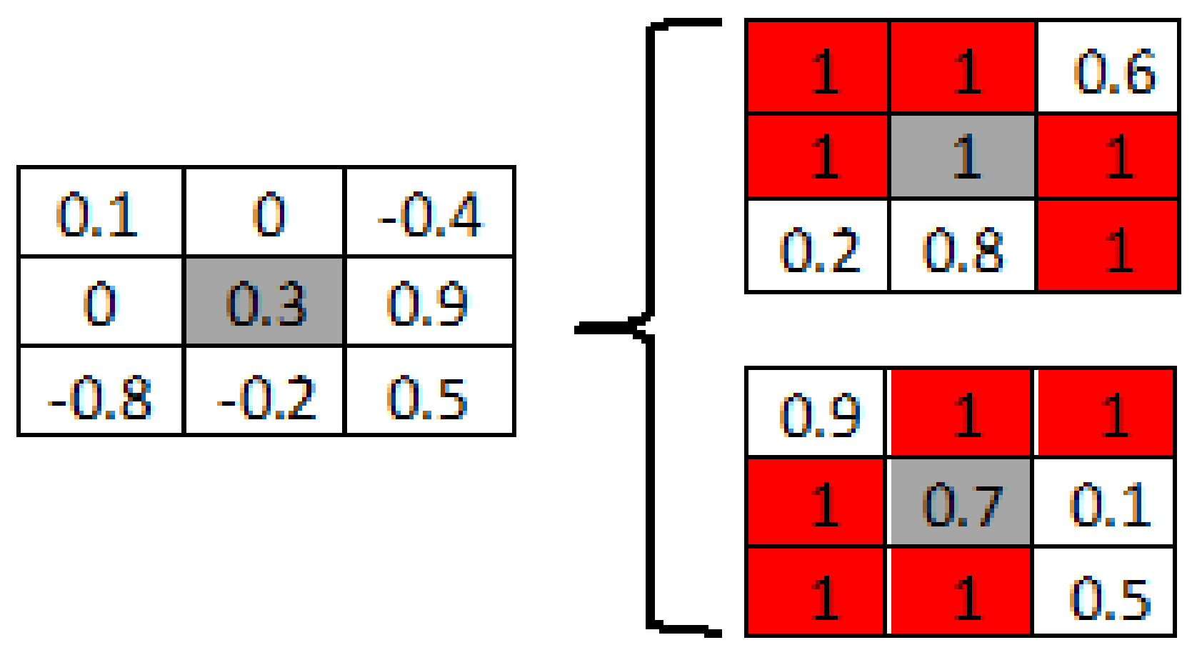
2.3. Mapping Transformation (MT)

A MT method is proposed in this paper as an efficient rescuer of memristor-based DNNs from accuracy degradation, and energy and latency overhead. According to the conventional mapping, algorithmic weights ranging from [−1, 1] are mapped on the memristor arrays based on the resistance state [LRS, HRS]. The MT method changes that range and re-initiates it from [0, 1] based on the same [LRS, HRS]; that is, an original weight is split into two positive weights and then mapped on two memristors. A subtractor is used to extract the original weight during computation as shown in Figure 2. The algorithm for weight W in MT method is as follows:
W a = 1 W 0 , 1 | W | W < 0 ,
W b = 1 W W > 0 , 1 W 0 ,
where W a and W b are the two parts of a single weight that will be stored in two memristors. Moreover, during the computation, the original weight will be extracted from two memristors through a subtraction ( W a W b ) .
Figure 2 represents the hardware implementation of the proposed MT method. Here, the weights W a , W b will be mapped on two memristors according to the cells resistive level R a and R b , respectively. Then, an Op-Amp-based subtractor is used to subtract the weights during the computation [27].
For example, as shown in Figure 4, weight 0.3 from the algorithm will be mapped as 1 and 0.7 on two new memristors. At the end, a subtractor is used to get final weights resulting from 1–0.7. Actually, there are no “1” in the original memristor array, but in two new arrays, eleven “1” are generated and “1” is 11/18 of two new arrays. From Figure 4, it can also be interpreted that most of the newly mapped weights on memristors are at HRS (“1”), and such creations of “1” on memristor arrays will generate significant overlaps between such HRS and SA1, which in turn suppresses the accuracy degradation caused by the SA1.
Additionally, the MT method can be effective to manage energy and latency. Even though the MT method uses two memristors to represent one weight, it consumes less energy than that in the conventional mapping. For example, as shown in Figure 4, the conventional mapping method will map weight 0.3 (LRS) directly to one memristor. However, after MT method is applied, two memristors—1 (HRS) and 0.7 (HRS)—are utilized. According to Equation (1), HRS means higher resistance R and lower energy consumption, because 1 / 0.3 > 1 / 1 + 1 / 0.7 . As for the latency, in the MT method, two new memristors are being read simultaneously during computation, not one after another. Therefore, the MT method is always reported to have constant latency just like a fault-free memristor array.

3. Result and Discussion

In order to evaluate the proposed MT method, the DNN+NeuroSim platform is utilized in this paper. DNN+NeuroSim is an integrated framework that emulates inference performance or on-chip training performance on in-memory computing architecture [28]. Especially, an 8-layer VGG network with CIFAR-10 dataset is employed in DNN+NeuroSim to provide accuracy, energy, and latency results of the hardware for our work. Most importantly, DNN+NeuroSim is based on the real device: 40 nm A g : a- S i memristor. As shown in Figure 5, the fabricated memristor with Silver ( A g ) and Silicon ( S i ), as an active layer, is tested and its current-pulse characteristics, maximum/minimum resistance, non-linearity, and number of conductance level are utilized in DNN+NeuroSim for system evaluations. The curves indicates that the memristor is programmed by consecutive 100 identical positive (LTP, 3.2 V, 300 μs) pulses followed by consecutive 100 identical negative pulses (LTD, −2.8 V, 300 μs) [8]. The conductance is measured at 1 V just after each programmed pulse and the read current is plotted. In addition, in order to consider the impact of some hidden dynamics, such as the inter-cycle variability of a memristor, the standard/Gaussian distribution N ( μ , σ ) is used in all our experiments on the DNN+NeuroSim. σ is set as 0.3% for such an inter-cycle variability according to testing results of manufactured memristors in Figure 5.

3.1. Weight Distribution with MT

The MT method turns out to be efficient in restoring accuracy as well as controlling the energy and latency. As SAFs are sporadic and the ratio of SA1 and SA0 can vary, we will analyze two typical SA1:SA0 ratios, 5:1, and 1:5, to cover most scenarios. Algorithm 1 shows the pseudocode of the MT method. Taking the same VGG-8 model trained by CIFAR-10 dataset as an example, after the MT is applied, the weight distribution of the model changes as shown in Figure 6. Two new arrays totally include 12.97 × 2 million memristors. In one array, the number of “1” is 7.35 million as 56.67% of all elements. The other array contains 9.65 million of “1” which is 74.40% of all elements. Totally, more than 18 million “1” are created which is 65.54% of the total weights. In addition, more than 7 million (34.46%) weights are greater than or equal to 0.9 and less than 1.
As a huge number of “1” is mapped on the memristor array, most of the SA1 will be overlapped with the newly generated “1”. Besides, newly generated 34.46% of memristors are also closer to 1, and if SAFs happen to this 34.46% of cells, the damage will be insignificant.
Alogirithm 1. Mapping Transformation
Jlpea 12 00010 i001

3.2. Impact of MT Method

3.2.1. Accuracy

Before applying the MT method, SAFs are introduced in the memristor array. As listed in Table 1 and Table 2, the accuracy exponentially degrades. Under as small as 2.5% SAFs with both SA1:SA0 = 5:1 and SA1:SA0 = 1:5, DNNs are damaged completely and provided 10% accuracy which is merely equivalent to a random guessing.
After applying the MT method, from Table 1 and Table 2, accuracies are regained to 90% in most of cases less than 2.5% SAFs. As the MT method is to transform most of the weights from 0 to 1 or closer to 1, it can regain maximum accuracy in those conditions where SA1 dominates SAFs. Therefore, it concludes that when applying the MT method for 20% SAFs, the DNN with SA1:SA0 = 5:1 regains the maximum accuracy of 88% due to the SA1 dominancy; the DNN with SA1:SA0 = 1:5 regains accuracy only to 63%, because SA1 becomes minor as compared to SA0. In addition, even under extremely high SAFs as 50% with SA1:SA0 = 5:1, the MT method still enables the DNN to have strong immunity to SAFs and restores up to as high as 80% accuracy.

3.2.2. Energy

In Table 1, SA1:SA0 = 5:1, and with the increment of the percentage of SAFs, the number of SA1 cells stuck at HRS increases. Before applying the MT method, with the increment in SA1, the R in Equation (1) will increase, and the total energy consumption should decrease. However, instead, a large number of SAFs cause energy overhead because of the coexistence of SA1 and SA0. In general, in a memristor-based DNN, the read circuit is designed to sense the resistance of a memristor and uses such resistance to represent the weight. Normally, a weight that represents LRS is assumed to have the lowest fixed-resistance state. As discussed in Section 2.1, the non-ideal manufacture and over forming causes SA0 in a memristor array, and the resistance of the overly formed memristors may become 10 times or 100 times lower than the normal LRS [4]. Therefore, those overly formed memristors may consume 10 times or 100 times more energy than memristors which are not defective and normally mapped to LRS, according to Equation (1). Such a level of the scale-up energy depends on how much the over forming causes the damage to a memristor and how much the resistance of a memristor is lower than the normal LRS. As a result, the energy consumed by memristor with SA0 will contribute much more to the energy overhead. As shown in Table 1, when SAFs are up to 2.5%, the energy can be controlled, and no overhead is generated. However, when SAFs are 20% and beyond, the SA0 in the memristor array increases a lot along with an increase of SAFs, and energy consumption enlarges to 240%.
Furthermore, the situation gets worse when SA1:SA0 is 1:5 as shown in Table 2. Even when SAF is as little as 1%, the dominant SA0 increases the energy overhead up to 336%. The comparison of Table 1 and Table 2 also give some insight regarding the deteriorating impact of more SA0 in the memristor array. The maximum energy consumption listed in Table 2 is 9.54 × 10 5 J (SA1:SA0 = 1:5) which is almost 34% higher than the maximum energy listed in Table 1, 7.13 × 10 5 J (SA1:SA0 = 5:1).
However, after applying the MT method, the memristor array acts like a fault-free device even in presence of significant SAFs. The MT method completely controls the energy overhead. This is because the MT method uses two memristors ( R a ) and ( R b ) to represent one weight, and the original algorithmic weight value (R) is extracted at the end, as shown in Figure 2. Moreover, 1 / R > 1 / R a + 1 / R b . As a result, the energy consumption with the MT method listed in Table 1 and Table 2 are much decreased as compared with that before the MT method is applied.
In addition, weights in Figure 6 actually show less standard deviations as compared with weights in Figure 3. This means that after the MT method is applied, the weight distribution is more average in the entire memristor array than before, therefore it avoids hot spots and improve the thermal stability of the array.

3.2.3. Latency

Latency is defined as the time required for the output voltage to reach the switching voltage threshold after the input voltage reaches the memristor [26]. It can be calculated by using the Horowitz equation:
L a t e n c y = τ f ln ( v s ) 2 + 2 β ( 1 v s ) r a m p I n p u t × τ f
where v s and r a m p I n p u t are the normalized switching voltage threshold (typically 0.5) and input voltage ramp rate. β = 1 / ( g m R ) is the reciprocal of the normalized input transconductance times the output resistance R. τ f is the total R C time constant at the output node. Therefore, Equation (4) can be transferred as
L a t e n c y = R C ln ( v s ) 2 + 2 ( 1 v s ) r a m p I n p u t × R C × g m R
Therefore, L a t e n c y m R 2 C 2 + n C . m and n are constants. The total latency is calculated as the sum of gate level latency of all sub-circuits [29].
Similar with the energy analysis, as shown in Table 1 and Table 2, before applying the MT method, the DNN with 0.1% SAFs nearly fails to generate the latency overhead. However, with SAFs increasing, an increasing number of defective memristors with a bigger R C are inserted to replace original memristors, and then the latency becomes much larger than before. As listed in Table 1, under 20% SAFs with SA1:SA0 = 5:1 and 1.0% SAFs with SA1:SA0 = 1:5, the latency enlarges about 2 times than before.
However, after the MT is applied, as listed in Table 1 and Table 2, the latency remains the same, because total R = R a + R b , that removes the energy overhead. Furthermore, in the memristor-based DNN, the weight tuning is also included in the latency calculation [26]. This value can add extra latency in the conventional mapping method. However, after applying the MT method, approximately 65.54% of weights will almost always be mapped to 1 as shown in Figure 6, and they do not go through the tuning process. Therefore, this additional feature can also highly contribute to remove latency overhead.

3.3. Immunity of Mapping Transformation Method against Non-Linearity

3.3.1. Accuracy

DNN models are very sensitive to weights which are updated frequently [30]. A small weight deviation between model and actual memristor can degrade the accuracy significantly. Apart from SAFs, memristors also suffer from non-linearity that generates inaccurate weight updating [19,31]. Applying a positive voltage pulse to a memristor that causes a change in resistance from LRS towards HRS is defined as long-term potentiation (LTP). Similarly, a negative voltage pulse to a memristor that causes a change in resistance from HRS towards LRS is defined as long-term depression (LTD) [32]. When LTP = LTD = 0, the memristor is ideal and no non-linearity exists. However, in practice, non-linearity cannot be completely avoided, therefore, as for experiments in Table 1 and Table 2, the non-linearity is considered as LTP = 1.75 and LTD = −1.46. When further non-linearity as LTP = 4 and LTD = −4, as listed in Table 3 and Table 4, is introduced in memristor arrays, as compared with results with LTP = 1.75 and LTD = −1.46, accuracies degrade more. For example, in Table 1 and Table 2, when SA1:SA0 = 5:1/1:5, the accuracies are 90%/88% with 0.1% SAF, but it is only 65%/53% in Table 3 and Table 4.
The MT method shows the excellence in restoring the accuracy even under extreme non-linearity (LTP = 4, LTD = −4). As listed in Table 3 and Table 4, after MT is applied, the accuracy increased to 71% from 10% with 1% SAF under SA1:SA0 = 5:1. Similarly, the accuracy increased to 69% from 10% with 1% SAF under SA1:SA0 = 1:5. This is because, according to the MT method, 65.54% memristors are mapped to “1” (HRS), as shown in Figure 6. Moreover, such “1” (HRS), even for different LTP and LTD, were nearly identical, as shown in Figure 7. Accordingly, those HRS cells are barely influenced by such non-linearity. In addition, as shown in Figure 6, only 34.46% memristors are mapped to sub-1 (less than 1 but greater than or equal 0.9). Although these sub-1 are influenced by the non-linearity, as compared with the original weights before the MT method is applied, their differences are not significant as shown in Figure 7. Therefore, even with the large non-linearity LTP = 4 and LTD= −4, as for the various SAF conditions, the inference accuracies can be greatly restored.

3.3.2. Energy and Latency

Unlike accuracy, the impact of non-linearity to energy and latency is not significant. For instance, two ideal memristor with LTP = 0 and LTD = 0 provide two resistance state A and B respectively after applying a certain number of pulses as shown in Figure 7. When LTP = 4, the resistance state A will change to C, which indicates the resistance increases faster and decrease energy/latency, according to Equations (1) and (4). However, when LTD = −4, the resistance state B will change to D, which indicates the resistance decreases faster and increase energy/latency, according to Equations (1) and (4). This trade-off will make the average energy/latency keep the same. As listed in Table 1, Table 2, Table 3 and Table 4, even under different non-linearity, when the MT method is applied, the energy/latency have no noticeable changes. In a word, the MT method can still effectively eradicate the energy/latency overhead by mapping most of the cells to HRS even with high non-linearity LTP = 4 and LTD = −4.

4. Comparison

As listed in Table 5, compared with the state-of-the-art, our proposed method has some advantages. To date, other works on handling SAF defects require an additional algorithm or individual optimization because most of them need to first identify the defective cells and the most significant weights. Then, they map those weights to the fault-free regions or cells. Additionally, in other works, a complex control circuit is required which generates the significant circuitry overhead. Our proposed MT method creates a universal solution that would work in any memristor device irrespective of the randomness of the SAF defects. It is significantly functional even in extreme SAF cases (50% SAFs) without adding large peripheral circuits. Furthermore, the energy consumption and latency are thoroughly analyzed in our work before and after MT is applied to exhibit the characteristics of memristor-based DNNs in different SAF conditions which the other works often overlook.

5. Conclusions

Memristors are popular for the DNN hardware design and have demonstrated their potential in boosting the speed and energy efficiency of analog matrix-vector multiplication. However, commonly occurring Stuck-At-Faults (SAFs) seriously degrade inference accuracies of memristor-based DNNs. In this paper, a MT method is proposed to mitigate Stuck-at-Fault (SAF) defects. Based on the VGG8 model with the CIFAR10 dataset, the experiment results show that the MT method can recover the DNN to its original inference accuracy (90%) when the ratio of SAFs is smaller than 2.5%. Moreover, even when SAFs with SA1:SA0 = 5:1 is in the extreme condition of 50%, it is still highly efficient to recover the inference accuracy to 80%. In addition, the MT method removes all overhead of energy and latency even when SAFs hold a large ratio and are associated with high non-linearity LTP = 4 and LTD = −4. Finally, a detailed comparison with the state-of-the-art is provided to indicate some advantages of our proposed method.

Author Contributions

Conceptualization, G.Y., Z.L., J.F., C.D., Y.W. and J.W.; methodology, M.O.-U.-Z., S.A.K., G.Y., Z.L., J.F. and J.W.; software, M.O.-U.-Z. and S.A.K.; validation, M.O.-U.-Z., S.A.K. and J.W.; data curation, M.O.-U.-Z. and S.A.K.; writing—original draft preparation, M.O.-U.-Z. and S.A.K.; writing—review and editing, J.W.; supervision, J.W.; project administration, J.W.; funding acquisition, J.W. All authors have read and agreed to the published version of the manuscript.

Funding

This work was funded in part by the National Science Foundation under Grant 1953544 and Grant 1855646.

Data Availability Statement

The data presented in this study are available in article.

Conflicts of Interest

The authors declare no conflict of interest.

Abbreviations

The following abbreviations are used in this manuscript:
CMOSComplementary Metal Oxide Semiconductor
DNNDeep Neural Network
MTMapping Transformation
IoTInternet of Things
AIArtificial Intelligence
SAFStuck-at-Fault

References

  1. Shi, W.; Dustdar, S. The promise of edge computing. Computer 2016, 49, 78–81. [Google Scholar] [CrossRef]
  2. Fu, J.; Liao, Z.; Liu, J.; Smith, S.C.; Wang, J. Memristor-Based Variation-Enabled Differentially Private Learning Systems for Edge Computing in IoT. IEEE Internet Things J. 2020, 8, 9672–9682. [Google Scholar] [CrossRef]
  3. Liu, F.; Ju, X.; Wang, N.; Wang, L.; Lee, W.J. Wind farm macro-siting optimization with insightful bi-criteria identification and relocation mechanism in genetic algorithm. Energy Convers. Manag. 2020, 217, 186–198. [Google Scholar] [CrossRef]
  4. Williams, R.S. What’s Next? [The end of Moore’s law]. Comput. Sci. Eng. 2017, 19, 7–13. [Google Scholar] [CrossRef]
  5. Waldrop, M.M. The chips are down for Moore’s law. Nat. News 2016, 530, 144–147. [Google Scholar] [CrossRef] [Green Version]
  6. Chua, L. Memristor-the missing circuit element. IEEE Trans. Circuit Theory 1971, 18, 507–519. [Google Scholar] [CrossRef]
  7. Strukov, D.B.; Snider, G.S.; Stewart, D.R.; Williams, R.S. The missing memristor found. Nature 2008, 453, 80–83. [Google Scholar] [CrossRef]
  8. Jo, S.H.; Chang, T.; Ebong, I.; Bhadviya, B.B.; Mazumder, P.; Lu, W. Nanoscale memristor device as synapse in neuromorphic systems. Nano Lett. 2010, 10, 1297–1301. [Google Scholar] [CrossRef]
  9. Jo, S.H.; Lu, W. CMOS compatible nanoscale nonvolatile resistance switching memory. Nano Lett. 2008, 8, 392–397. [Google Scholar] [CrossRef]
  10. Oblea, A.S.; Timilsina, A.; Moore, D.; Campbell, K.A. Silver chalcogenide based memristor devices. In Proceedings of the International Joint Conference on Neural Networks (IJCNN), Barcelona, Spain, 18–23 July 2010; pp. 1–3. [Google Scholar]
  11. Prodromakis, T.; Michelakis, K.; Toumazou, C. Fabrication and electrical characteristics of memristors with TiO2/TiO2+x active layers. In Proceedings of the IEEE International Symposium on Circuits and Systems, Paris, France, 30 May–2 June 2010; pp. 1520–1522. [Google Scholar]
  12. Chen, C.Y.; Shih, H.C.; Wu, C.W.; Lin, C.H.; Chiu, P.F.; Sheu, S.S.; Chen, F.T. RRAM defect modeling and failure analysis based on march test and a novel squeeze-search scheme. IEEE Trans. Comput. 2014, 64, 180–190. [Google Scholar] [CrossRef]
  13. Kvatinsky, S.; Friedman, E.G.; Kolodny, A.; Weiser, U.C. TEAM: Threshold adaptive memristor model. IEEE Trans. Circuits Syst. I Regul. Pap. 2012, 60, 211–221. [Google Scholar] [CrossRef]
  14. Pickett, M.D.; Williams, R.S. Sub-100 fJ and sub-nanosecond thermally driven threshold switching in niobium oxide crosspoint nanodevices. Nanotechnology 2012, 23, 1–7. [Google Scholar] [CrossRef] [PubMed]
  15. Torrezan, A.C.; Strachan, J.P.; Medeiros-Ribeiro, G.; Williams, R.S. Sub-nanosecond switching of a tantalum oxide memristor. Nanotechnology 2011, 22, 485203. [Google Scholar] [CrossRef] [PubMed]
  16. Lee, M.J.; Lee, C.B.; Lee, D.; Lee, S.R.; Chang, M.; Hur, J.H.; Kim, Y.B.; Kim, C.J.; Seo, D.H.; Seo, S.; et al. A fast, high-endurance and scalable non-volatile memory device made from asymmetric Ta2O5-x/TaO2-x bilayer structures. Nat. Mater. 2011, 10, 625–630. [Google Scholar] [CrossRef]
  17. Pi, S.; Lin, P.; Xia, Q. Cross point arrays of 8 nm × 8 nm memristive devices fabricated with nanoimprint lithography. J. Vac. Sci. Technol. B Nanotechnol. Microelectron. Mater. Process. Meas. Phenom. 2013, 31, 06FA02. [Google Scholar] [CrossRef]
  18. Xia, Q.; Robinett, W.; Cumbie, M.W.; Banerjee, N.; Cardinali, T.J.; Yang, J.J.; Wu, W.; Li, X.; Tong, W.M.; Strukov, D.B.; et al. Memristor- CMOS hybrid integrated circuits for reconfigurable logic. Nano Lett. 2009, 9, 3640–3645. [Google Scholar] [CrossRef]
  19. Fu, J.; Liao, Z.; Gong, N.; Wang, J. Mitigating nonlinear effect of memristive synaptic device for neuromorphic computing. IEEE J. Emerg. Sel. Top. Circuits Syst. 2019, 9, 377–387. [Google Scholar] [CrossRef]
  20. Liu, C.; Hu, M.; Strachan, J.P.; Li, H. Rescuing memristor-based neuromorphic design with high defects. In Proceedings of the 54th ACM/EDAC/IEEE Design Automation Conference (DAC), Austin, TX, USA, 18–22 June 2017; pp. 1–6. [Google Scholar]
  21. Chen, L.; Li, J.; Chen, Y.; Deng, Q.; Shen, J.; Liang, X.; Jiang, L. Accelerator-friendly neural-network training: Learning variations and defects in RRAM crossbar. In Proceedings of the Design, Automation & Test in Europe Conference & Exhibition (DATE), Lausanne, Switzerland, 27–31 March 2017; pp. 19–24. [Google Scholar]
  22. Zhang, B.; Uysal, N.; Fan, D.; Ewetz, R. Handling stuck-at-fault defects using matrix transformation for robust inference of dnns. IEEE Trans. Comput.-Aided Des. Integr. Circuits Syst. 2019, 39, 2448–2460. [Google Scholar] [CrossRef]
  23. Xia, L.; Huangfu, W.; Tang, T.; Yin, X.; Chakrabarty, K.; Xie, Y.; Wang, Y.; Yang, H. Stuck-at fault tolerance in RRAM computing systems. IEEE J. Emerg. Sel. Top. Circuits Syst. 2017, 8, 102–115. [Google Scholar] [CrossRef]
  24. Xia, L.; Liu, M.; Ning, X.; Chakrabarty, K.; Wang, Y. Fault-tolerant training with on-line fault detection for RRAM-based neural computing systems. In Proceedings of the 54th Annual Design Automation Conference, Austin, TX, USA, 18–22 June 2017; pp. 1–6. [Google Scholar]
  25. Yeo, I.; Chu, M.; Gi, S.G.; Hwang, H.; Lee, B.G. Stuck-at-fault tolerant schemes for memristor crossbar array-based neural networks. IEEE Trans. Electron Devices 2019, 66, 2937–2945. [Google Scholar] [CrossRef]
  26. Chen, P.Y.; Peng, X.; Yu, S. NeuroSim: A circuit-level macro model for benchmarking neuro-inspired architectures in online learning. IEEE Trans. Comput.-Aided Des. Integr. Circuits Syst. 2018, 37, 3067–3080. [Google Scholar] [CrossRef]
  27. Krestinskaya, O.; James, A.P.; Chua, L.O. Neuromemristive circuits for edge computing: A review. IEEE Trans. Neural Netw. Learn. Syst. 2019, 31, 4–23. [Google Scholar] [CrossRef] [PubMed] [Green Version]
  28. Peng, X.; Huang, S.; Jiang, H.; Lu, A.; Yu, S. DNN+ NeuroSim V2. 0: An end-to-end benchmarking framework for compute-in-memory accelerators for on-chip training. IEEE Trans. Comput.-Aided Des. Integr. Circuits Syst. 2020, 40, 2306–2319. [Google Scholar] [CrossRef]
  29. Liao, Z.; Fu, J.; Wang, J. Ameliorate Performance of Memristor Based ANNs in Edge Computing. IEEE Trans. Comput. 2021, 70, 1299–1310. [Google Scholar] [CrossRef]
  30. QueryNet: Querying neural networks for lightweight specialized models. Inf. Sci. 2022, 589, 186–198. [CrossRef]
  31. Gaudet, V. A survey and tutorial on contemporary aspects of multiple-valued logic and its application to microelectronic circuits. IEEE J. Emerg. Sel. Top. Circuits Syst. 2016, 6, 5–12. [Google Scholar] [CrossRef]
  32. Chen, P.Y.; Lin, B.; Wang, I.T.; Hou, T.H.; Ye, J.; Vrudhula, S.; Seo, J.S.; Cao, Y.; Yu, S. Mitigating effects of non-ideal synaptic device characteristics for on-chip learning. In Proceedings of the IEEE/ACM International Conference on Computer-Aided Design (ICCAD), Austin, TX, USA, 2–6 November 2015; pp. 194–199. [Google Scholar]
  33. Jung, G.; Fouda, M.; Lee, S.; Lee, J.; Eltawil, A.; Kurdahi, F. Cost- and Dataset-free Stuck-at Fault Mitigation for ReRAM-based Deep Learning Accelerators. In Proceedings of the Design, Automation, Test in Europe Conference Exhibition (DATE), Grenoble, France, 1–5 February 2021; pp. 1733–1738. [Google Scholar]
  34. Zhang, J.; Kline, D.; Fang, L.; Melhem, R.; Jones, A.K. Dynamic partitioning to mitigate stuck-at faults in emerging memories. In Proceedings of the IEEE/ACM International Conference on Computer-Aided Design (ICCAD), Irvine, CA, USA, 13–16 November 2017; pp. 651–658. [Google Scholar]
  35. Charan, G.; Mohanty, A.; Du, X.; Krishnan, G.; Joshi, R.V.; Cao, Y. Accurate Inference With Inaccurate RRAM Devices: A Joint Algorithm-Design Solution. IEEE J. Explor.-Solid-State Comput. Devices Circuits 2020, 6, 27–35. [Google Scholar] [CrossRef]
  36. He, Z.; Lin, J.; Ewetz, R.; Yuan, J.S.; Fan, D. Noise Injection Adaption: End-to-End ReRAM Crossbar Non-ideal Effect Adaption for Neural Network Mapping. In Proceedings of the 56th ACM/IEEE Design Automation Conference (DAC), Las Vegas, NV, USA, 2–6 June 2019; pp. 1–6. [Google Scholar]
Figure 1. Memristor crossbar arrays for matrix-vector multiplications.
Jlpea 12 00010 g001
Figure 2. Hardware implementation for Mapping Transformation (MT) method.
Jlpea 12 00010 g002
Figure 3. Weight distribution of VGG8 model trained by CIFAR10 dataset.
Jlpea 12 00010 g003
Figure 4. Mapping Transformation (MT) method.
Jlpea 12 00010 g004
Figure 5. A g : a- S i based memristor Device.
Jlpea 12 00010 g005
Figure 6. Weight distribution of VGG8 model after MT method is applied.
Jlpea 12 00010 g006
Figure 7. Non-linearity in memristor cells device.
Jlpea 12 00010 g007
Table 1. Energy and latency comparison when SA1:SA0 = 5:1.
SAF
(SA1 & SA0)
Before MT a After MT
Energy (J)Latency (s)AccuracyEnergy (J)Latency (s)Accuracy
0.1%2.550 × 10 5 66.490 × 10 5 90%2.334 × 10 5 66.395 × 10 5 90%
1.0%2.550 × 10 5 66.499 × 10 5 42%2.335 × 10 5 66.401 × 10 5 90%
2.5%2.550 × 10 5 66.479 × 10 5 10%2.335 × 10 5 66.398 × 10 5 90%
20%7.130 × 10 5 12.019 × 10 4 10%2.330 × 10 5 66.397 × 10 5 88%
50%7.127 × 10 5 12.019 × 10 4 10%2.311 × 10 5 66.397 × 10 5 80%
MTa: Mapping Transformation.
Table 2. Energy and latency comparison when SA1:SA0 = 1:5.
SAF
(SA1 & SA0)
Before MT a After MT
Energy (J)Latency (s)AccuracyEnergy (J)Latency (s)Accuracy
0.1%2.542 × 10 5 66.465 × 10 5 88%2.335 × 10 5 66.397 × 10 5 90%
1.0%9.542 × 10 5 12.019 × 10 4 10%2.336 × 10 5 66.401 × 10 5 90%
2.5%9.517 × 10 5 12.019 × 10 4 10%2.332 × 10 5 66.397 × 10 5 89%
20%9.035 × 10 5 12.019 × 10 4 10%2.274 × 10 5 66.387 × 10 5 63%
50%9.029 × 10 5 12.019 × 10 4 10%2.226 × 10 5 66.388 × 10 5 21%
MTa: Mapping Transformation.
Table 3. Energy and latency comparison with extreme non-linearity when SA1:SA0 = 5:1.
SAFBefore MT a LTP = 4, LTD = −4After MT LTP = 4, LTD = −4
Energy (J)Latency (s)AccuracyEnergy (J)Latency (s)Accuracy
0.1%2.494 × 10 5 66.445 × 10 5 65%2.287 × 10 5 66.354 × 10 5 71%
1.0%2.090 × 10 5 66.396 × 10 5 10%2.292 × 10 5 66.357 × 10 5 71%
2.5%2.187 × 10 5 66.421 × 10 5 10%2.286 × 10 5 66.358 × 10 5 70%
20%7.127 × 10 5 12.019 × 10 4 10%2.319 × 10 5 66.359 × 10 5 62%
50%7.126 × 10 5 12.019 × 10 4 10%2.322 × 10 5 66.365 × 10 5 50%
MTa: Mapping Transformation.
Table 4. Energy and latency comparison with extreme non-linearity when SA1:SA0 = 1:5.
SAFBefore MT a LTP = 4, LTD = −4After MT LTP = 4, LTD = −4
Energy (J)Latency (s)AccuracyEnergy (J)Latency (s)Accuracy
0.1%2.499 × 10 5 66.431 × 10 5 53%2.289 × 10 5 66.365 × 10 5 70%
1.0%9.327 × 10 5 12.019 × 10 4 10%2.298 × 10 5 66.359 × 10 5 69%
2.5%9.205 × 10 5 12.019 × 10 4 10%2.305 × 10 5 66.358 × 10 5 68%
20%9.031 × 10 5 12.018 × 10 4 10%2.309 × 10 5 66.366 × 10 5 30%
50%9.030 × 10 5 12.018 × 10 4 10%2.285 × 10 5 66.398 × 10 5 14%
MTa: Mapping Transformation.
Table 5. Comparison of the state-of-the-art.
Items[33][34][35][21][20][24][23][22][36][25]This Work
No Additional Algorithm×××××××××
No Individual Optimization××××××××
No Complex Control Circuit×××××
Extreme SAF Considerations (50%)×××××××××
Energy Analysis××××××××××
Latency Analysis××××××××××
Publisher’s Note: MDPI stays neutral with regard to jurisdictional claims in published maps and institutional affiliations.

