
A Time-Domain z−1 Circuit with Digital Calibration


Electronics Laboratory, Physics Department, University of Patras, 26504 Patras, Greece
*
Author to whom correspondence should be addressed.
J. Low Power Electron. Appl. 2022, 12(1), 3; https://0-doi-org.brum.beds.ac.uk/10.3390/jlpea12010003
Submission received: 4 November 2021
/
Revised: 25 December 2021
/
Accepted: 31 December 2021
/
Published: 3 January 2022
Abstract
:This paper presents a novel circuit of a z−1 operation which is suitable, as a basic building block, for time-domain topologies and signal processing. The proposed circuit employs a time register circuit which is based on the capacitor discharging method. The large variation of the capacitor discharging slope over technology process and chip temperature variations which affect the z−1 accuracy is improved using a novel digital calibration loop. The circuit is designed using a 28 nm Samsung FD-SOI process under 1 V supply voltage with 5 MHz sampling frequency. Simulation results validate the theoretical analysis presenting a variation of capacitor voltage discharging slope less than 5% over worst-case process corners for temperature between 0 °C and 100 °C while consuming only 30 μA. Also, the worst-case accuracy of z−1 operation is better than 33 ps for input pulse widths between 5 ns and 45 ns presenting huge improvement compared with the uncalibrated operator.
1. Introduction
The requirements for higher speed and lower power consumption are very important in many modern integrated circuit applications. These requirements are achieved by using state-of-art CMOS processes mainly due to the device sizes shrinking and the low voltage supplies. Unfortunately, smaller device sizes and low supplies make it more challenging for many of the traditional analog circuit topologies, such as analog-to-digital converters, to overcome the smaller voltage headroom and due to this there is worse dynamic range.
A time-domain approach is a relatively new approach which processes the time by means of a time delay, time difference or the pulse width instead of the voltage or current in conventional approaches. Therefore, the time is the quantity of interest in the time-domain circuits and systems [1].Time-domain is a very promising design approach even for such a scaled technology because it features a better trade-off between dynamic range and power consumption. The advantage of the time-domain systems is that they make use of the high-speed MOS devices, which means small time delay, and therefore process the time with higher resolution [2].
The main benefits of the time-domain design approach are the improved dynamic range and time resolution compared with the analog voltage or current mode circuits under the same low supply environment [2], and better power efficiency for the high-speed performance because they are mainly composed of CMOS digital building blocks (gates etc.) [3].
The z−1 operation belongs among the basic signal processing procedures in the traditional discrete-time digital signal processing (DT-DSP). In recent years the z−1 operation extended in the discrete-time continuous signal processing (DT-CSP) finding applications in time-domain circuits and systems [4]. DT-CSP needs a voltage-to-time (V/T) converter instead of an A/D converter which can be based on the well-known pulse-width modulation (PWM) or based on specific V/T converters [5,6].
In time-domain, the z−1 operation circuit can be based on circuits which are known as time register (TR) circuits. The main operation of the TR is to handle the time of the pulse width of the input pulses or time difference between the pulse edges, store this time and recover it when needed. It is assumed that the pulse-width is modulated by a voltage e.g., pulse-width is proportional to the input voltage. TR can be used in the construction of time-based arithmetic circuits such as time amplifiers [7,8,9], time adders/subtractors, time-integrators, time-to-digital converters [10,11,12] and time-domain processing blocks [13,14].
State-of-the-art time registers are based on two approaches. The first approach uses the single capacitor discharging through MOS devices [4] and the second employs on gated delay lines [15]. The first solution is more attractive compared to the inherent limitations of the gated delay lines since the circuit implementation is much simpler requiring fewer transistors, as well. The impact of leakage is the same between two solutions for high data rate cases [6].
The main problem of both solutions is the strong impact of the technology process (P) variations and chip temperature (T) variation (PT variations). The slope of the capacitor voltage discharging features strong variation over PT variations because of its dependency on the discharging drain current of a MOS device and the value on-chip capacitor. Any variation of the discharging slope unfortunately has a strong impact on the accuracy of the time storage by the TR circuit.
Our work proposes a z−1 circuit which is based on a novel time register [16]. The z−1 circuit topology employs four TR in series achieving high accuracy in the time storage generating also synchronized output pulses with the reference sampling clock. The discharging slope of the TR register is calibrated over PT variation using a novel digital loop. The digital loop can be disabled after the end of calibration cycles minimizing the current consumption of the entire circuit.
This paper is organized as follows. A short description of the proposed design aspects in respect of the combination of PWM with time-domain approach is presented in Section 2. The operation principle of the proposed time-register is described in Section 3. In Section 4, the proposed z−1 circuit is presented and analyzed while the associated digital calibration loop is analyzed in Section 5. The simulation results are reported in Section 6.
2. Pulse Width Modulation (PWM) and Time-Domain Approach
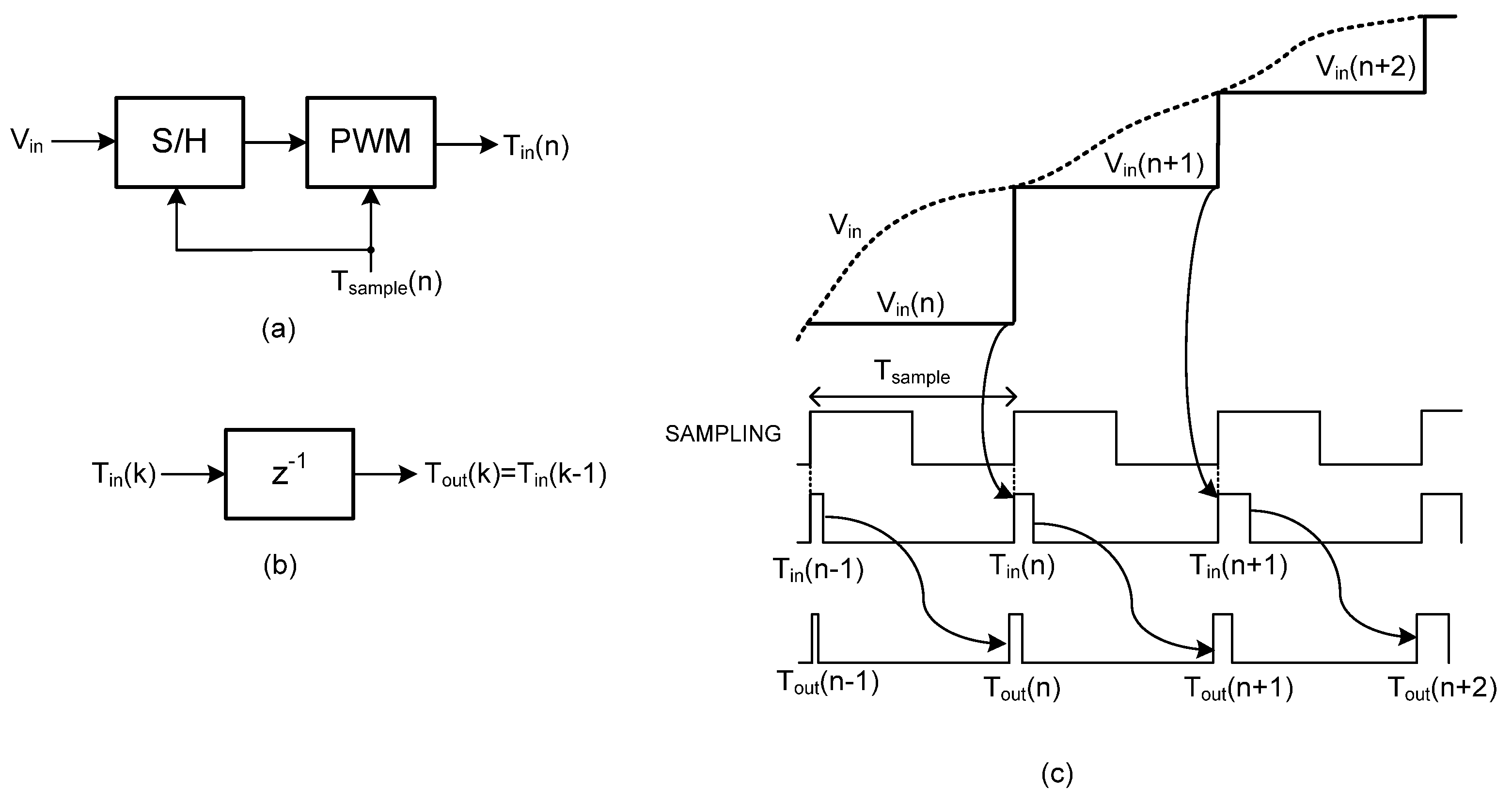
The time-domain circuits and systems mainly process the width of a pulse which is related to the information signal, for example, the input voltage VIN. The main procedure to convert Vin to a corresponding pulse width Tin is achieved using the pulse width modulation (PWM) technique [17]. The input signal which is in the voltage domain is firstly sampled using a sample and hold circuit (S/H). As shown in Figure 1a, the input voltage is maintained for a time interval equal to the sampling period Tsampling. The output of the PWM modulator is a pulse train with frequency equal to the sampling frequency with pulse width proportional to Vin.
Afterward, the signal is processed by various time-domain operators which can handle the pulse width of a pulse train. Among the most important operations in the time-domain systems is the delay of the input information, Tin in our case, by one clock of the sampling period, in other words the z−1 operation. Figure 1b presents a conceptual diagram of a z−1 operator. As depicted in Figure 1c, S/H produces the samples of Vin(n) and the PWM converts them into a pulse train with different pulse width Tin(n) for each sampling period. Tin(n) is fed to the z−1 operator and then the signal is delayed by the foul clock cycle of the sampling frequency.
3. Operation of Novel Time Register
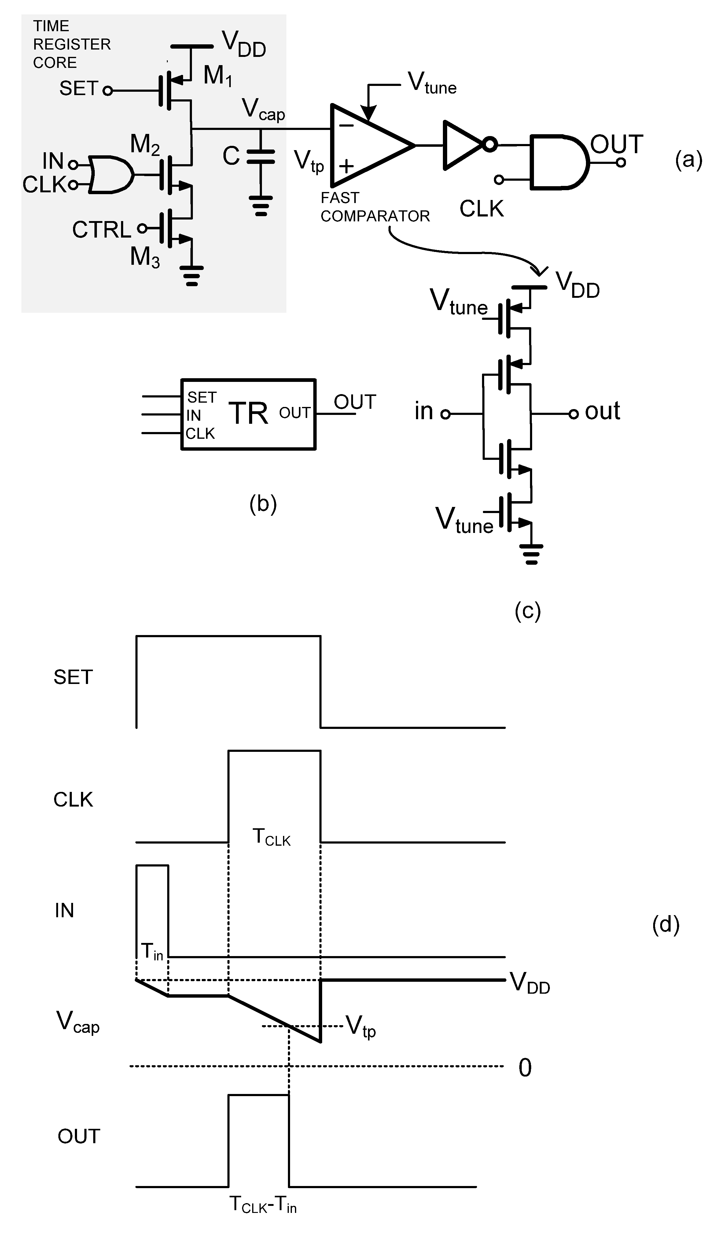
Figure 2a depicts the time register circuit, which is based on the study [16]. Transistor M1 acts as a switch which when it is ON charges the capacitor to VDD, where VDD is the supply voltage. The OR gate sends a signal to the transistor M2 which acts also as a switch but when it is ON the capacitor discharges. M3 acts as a current source and controls the discharging slope through its gate voltage CTRL. As it will be explained in Section 5, the gate voltage CTRL of M3 can be used to calibrate the variation of the discharging slope through a digital calibration loop. To be more precise, when voltage CTRL decreases/increases the drain current decreases/increases as well, and therefore, the discharging slope value decreases/increases. Lastly, the AND gate combined with the fast comparator [16] and a NOT gate in order to synchronize the output with CLK. The fast comparator which is presented in Figure 2c, is based on a current starving topology and is designed for fast transient response while its triple point voltage Vtp is tuned to be equal to VDD/2 (0.5 V).
Figure 2d depicts the time register’s operational diagram. The time interval Tin is related with the input pulse IN, and it is equal to its pulse width. Time interval TCLK is a pulse with constant pulse width with 25% duty cycle of the SET signal. When the SET voltage is zero, it pulls up the capacitor voltage Vcap to the supply voltage VDD otherwise when SET is VDD the capacitor discharges due to OR gate when IN or CLK is VDD. When both IN and CLK are zero the capacitor voltage remains unchanged. Larger pulse width Tin of the IN signal means more discharging time due to Tin but on the other hand the discharging time due to CLK is always the same. TCLK is the time interval that the capacitor is permitted to discharge to VDD/2, assuming the discharging slope does not change while TCLK is constant. Therefore, when the capacitor is discharged by the IN signal then for larger Tin, the capacitor voltage becomes VDD/2 sooner compared to the discharged due to CLK. Concluding, the output of the circuit is a pulse with a time interval value of TCLK-Tin achieving in this manner the storing of the value of Tin while the output pulse is synchronized with CLK signal.
It should be mentioned here that the fast comparator triple point voltage is tuned over PT corners in order to increase the comparison accuracy [16]. For this purpose, the fast comparator is included in a calibration loop. The calibration loop generates an appropriate tuning voltage Vtune that modifies the current of the starved devices stabilizing in this manner the triple point voltage. Also, the device dimensions are chosen in order to increase the comparison speed minimizing the time delay of the output pulse.
4. Time-Domain z−1 Operator Circuit
The operation of the z−1 is to generate an output pulse with pulse width equal to Tin which is synchronized with the sampling signal. As discussed in the previous section, unfortunately a TR circuit can store the pulse width Tin of the IN signal in the form of an output pulse with pulse width equal to TCLK-Tin which is synchronized with CLK signal and with the sampling reference clock.
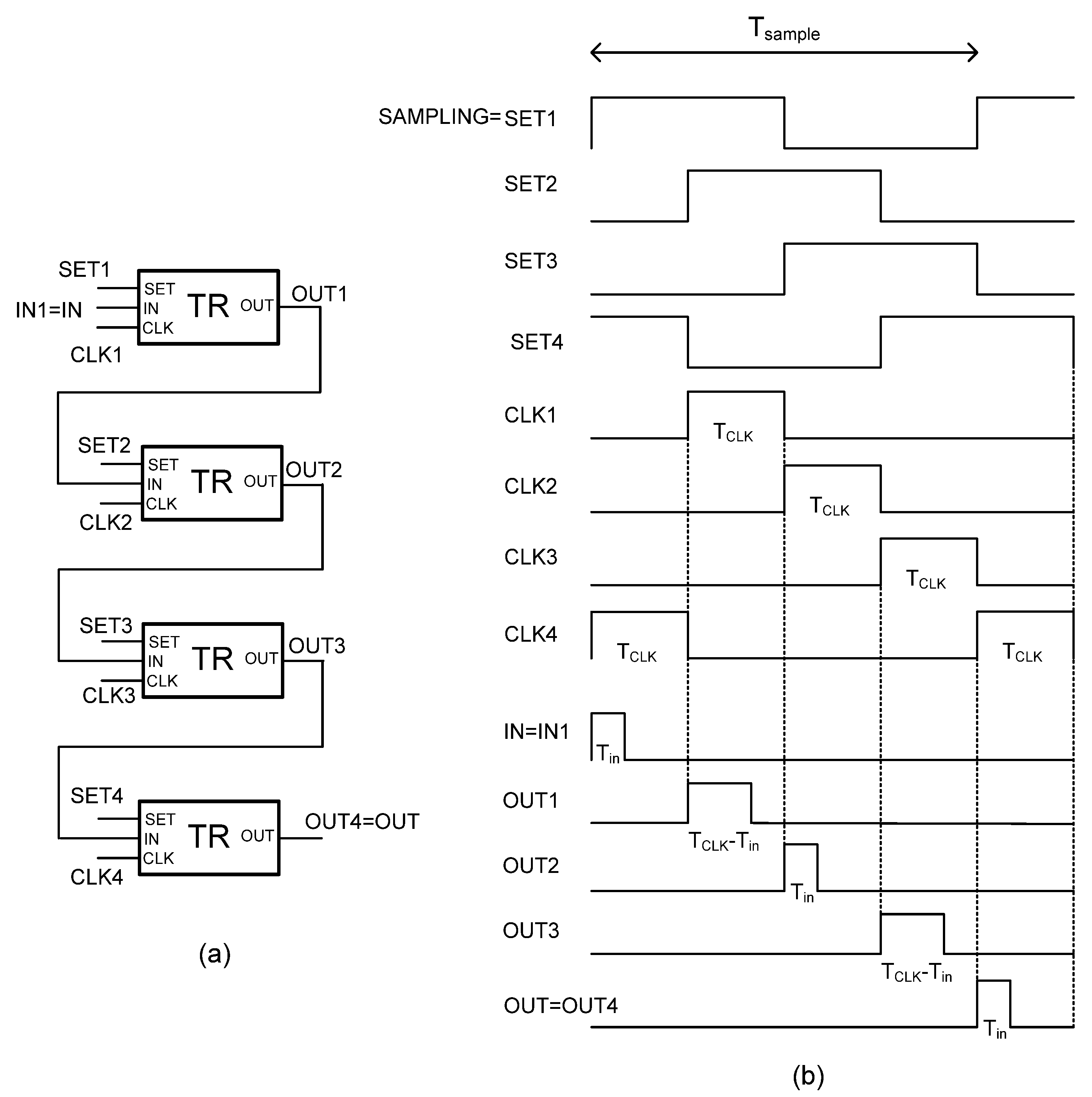
Figure 3a depicts the suggested z−1 circuit, and Figure 3b depicts the basic waveforms that illustrate its operation. A combination of four TR circuits series realizes a z−1 circuit. The SAMPLING signal is assumed to be the SET1 signal of the TR1 circuit, the input signal IN is equal to the input IN1 of TR1, while the final output signal OUT is the output of OUT4 of TR4.
The OUT1 pulse is generated at the rising edge of CLK1 in order to be synchronized with the SET2 pulse. Afterwards the OUT1 was used as input for the next TR. Therefore, TOUT2 = TCLK-TOUT1 = TCLK-(TCLK-Tin) = Tin and OUT2 is synchronized with CLK2. OUT2 is delayed by TSAMPLING/2 in relation to the sampling signal. Expanding the previous characteristic OUT4 pulse width is Tin and is delayed by TCLK. Taking this into consideration, by using in cascade placement of four TR the z−1 operator is created. Lastly, due to the subtraction that takes place after every TR constant error that can occur eliminate the others. Combining, z−1 circuits in series can create time-domain z−n operation, where n is the number of used z−1 operators. Also, other time-domain operations such as addition, subtraction and multiplication can be implemented with the proposed z−1 circuit [10].
5. Digital Calibration
As discussed in the previous section, the capacitor discharging slope of the TR must be calibrated against PT variations in order to increase the accuracy and the input dynamic range of the time registration.
The discharging slope depends on the ratio Idischarge/C, where Idischarge represents the discharging current (which is equal to the drain current M2) and C refers the capacitance. If the drain current of M2 is not calibrated, it can vary a lot between process and temperature corners. A current variation of around 20% is very common in the integrated bias current generators. In our procedure, the variance of the used capacitor is roughly 15%. Therefore, the slope variation without calibration is expected to have a lot of spread over corners. As a result, the capacitor voltage may drop excessively slowly in some corners without crossing the comparator’s triple point (0.5 V) during the CLK time interval. Even for minor Tin time interval, the capacitor voltage could cross the triple point in the event of a large discharge slope, reducing the dynamic range of TR. The calibration loop ensures the best operating condition, in which the capacitor crosses the triple point for a time interval equal to CLK. The digital loop ensures an almost dynamic range across process and temperature corners in this way.
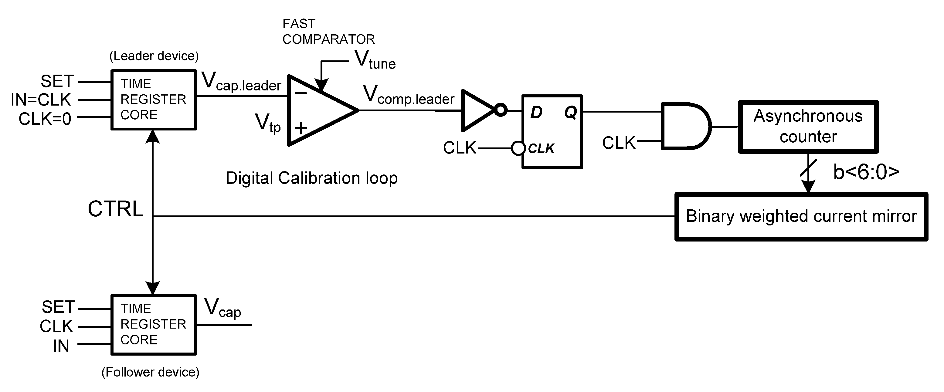
Figure 4 demonstrates the slope calibration architecture in an intuitive manner. A replica of the time register core circuit is used, which acts as leader device, where a) at the input port the clock signal is applied (IN = CLK) and b) at the clock input a zero voltage is applied (CLK = 0). As can be seen in Figure 2a, the CLK is applied to the gate of transistor M2 as a result of the OR gate. The inverted CLK signal is also applied to the clock of D flip-flop.
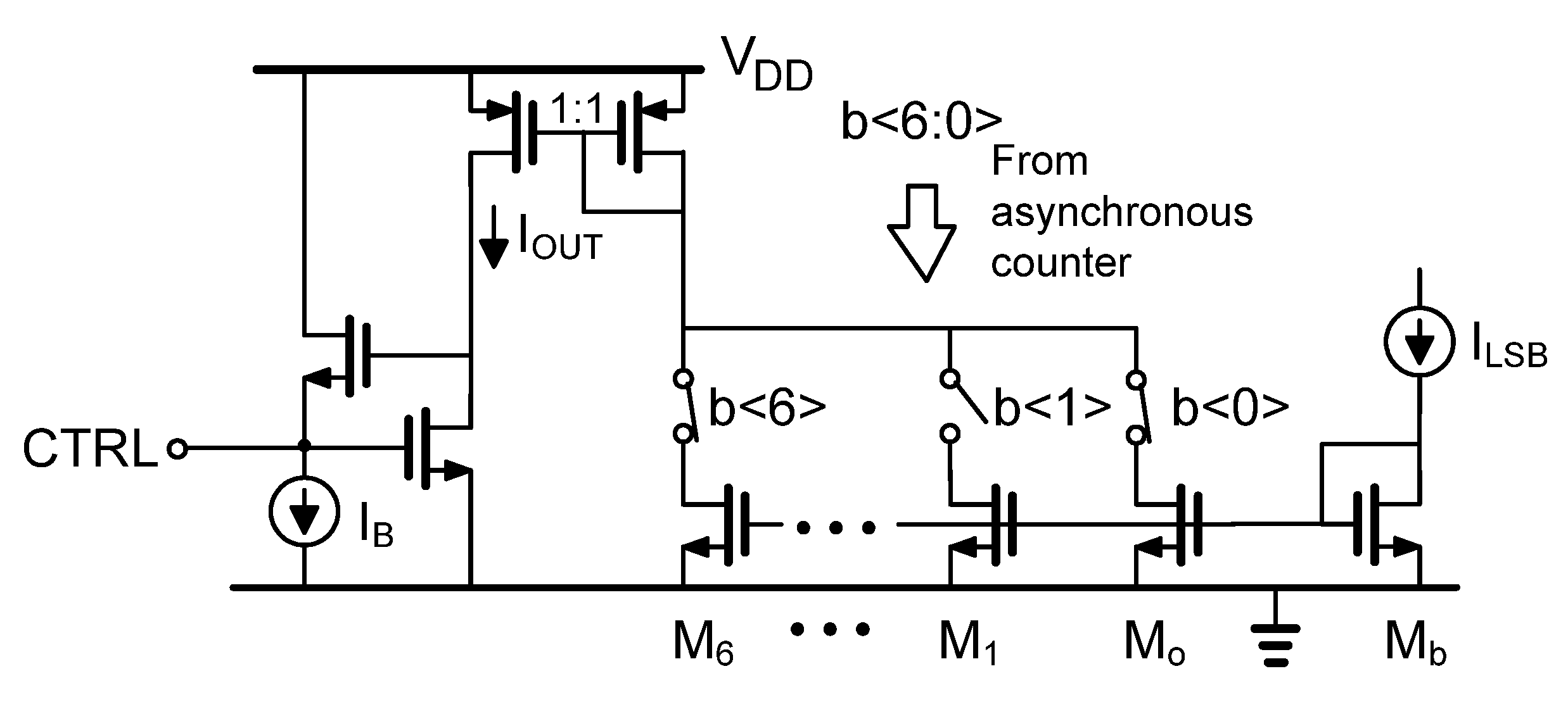
Figure 5 shows the digital loop, which includes an asynchronous counter and a digitally controlled binary-weighted current mirror. The output current is controlled by the digital word b<6:0> that comes from the asynchronous counter. The bias current ILSB defines the LSB current of the current mirror and is applied to the diode-connected transistor Mb. The channel width of transistors M0 to M6 increases in binary fashion.
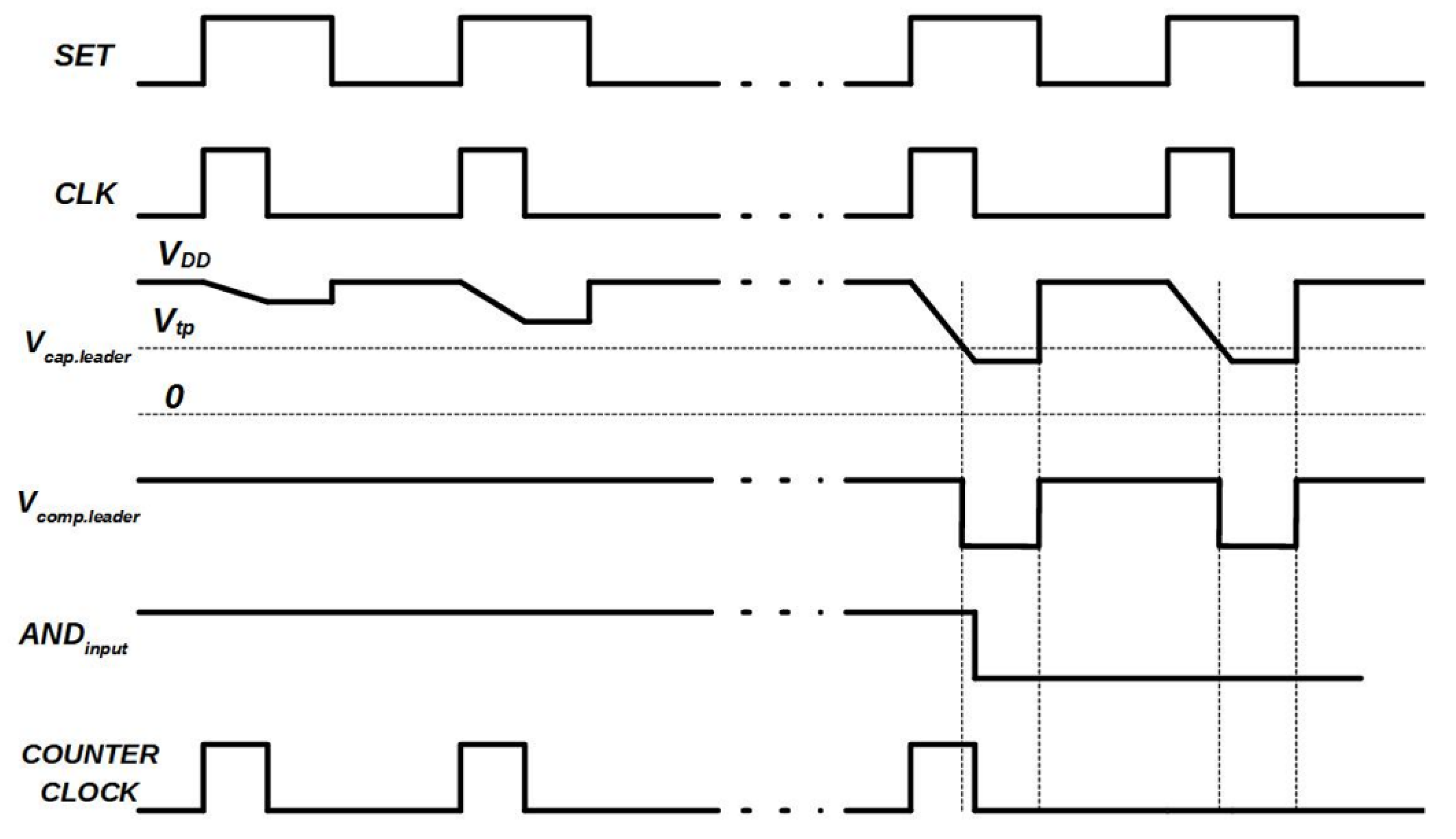
Figure 6 depicts the waveforms associated with the digital calibration Figure 6. The calibration loop is initialized as follows, (a) Vcap.leader is set to VDD (b) b<6:0> = 0,000,000 and (c) the output current of current mirror is set equal to zero and, therefore, the output of the comparator will be Vcomp.leader = VDD because Vcap.leader is larger than Vtp. Therefore, CLK through the AND gate is applied to the counter as a result (a) the digital output of asynchronous counter increases by one (b) the output of current mirror increases by an ILSB and (c) the discharging slope increases at each calibration cycle.
After several calibration cycles, Vcap.leader will be lower than Vtp the Vcomp.leader becomes zero. Therefore, when CLK = 0, at each calibration cycle, this will result in zero input of the AND gate, and the counter stops because CLK is not applied to the counter any more and stores the last digital word.
Afterwards, the current mirror uses this stored digital word and feeds the CTRL voltage to each time register core circuit adjusting in this way the discharging slope of each one. Voltage is used in order to increase the current driving capabilities of CTRL node avoiding also the coupling between each time register.
This approach to the calibration process eliminates the problem of the ripple that the previous paper presents [16] but introduces a problem due to quantization current. If the LSB of the current mirror is very large, big differences can be created between the CTRL of every PT corner. As a result, the design can be altered to fulfil the requirements. Moreover, by saving the digital word and applying the matching voltage to the follower time registers the calibration process can be terminated in order to save power.
6. Results
In the following section the efficiency of the proposed circuits is verified by simulation in Samsung 28 nm FD-SOI CMOS technology with a supply voltage of 1 V. The sampling frequency is 5 MHz. Also, the voltage triple point of comparator was adjusted to be 0.5 V.
6.1. Digital Calibration over Technology Process and Chip Temperature (PT) Corners
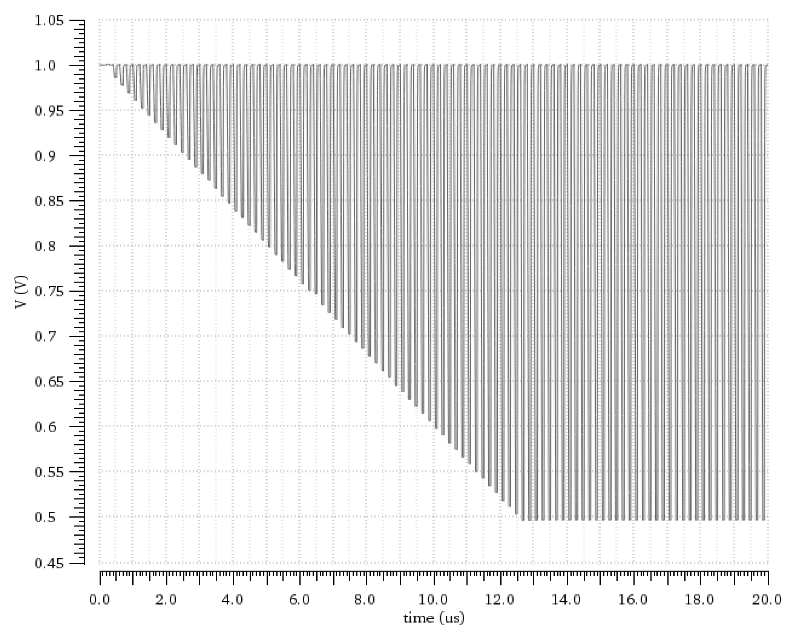
As discussed in the previous section, in this work the calibration of the time register is achieved by adjusting the value of the discharging current which is generated by the binary-weighted current mirror. Figure 7 illustrates the change of capacitor voltage during the calibration process. As expected, when calibration starts, Vcap is towards VDD with small discharging slope. In each calibration cycle the discharging slope increases because the current applied by the binary-weighted current mirrors increases and, therefore, Vcap moves towards Vtp which is set to 0.5 V. The calibration cycles continue until the Vcap crosses Vtp. Then, the discharging slope takes the right value and the calibration process stops storing at the same time as the last values of calibration bits, b<6:0>. It should be noted that the calibration process, as presented, in Figure 7 is for the typical process conditions at 27 °C; the calibration process is valid for all the PT corners. Due to the quantization error of the current mirror, the discharge slope of the corners slightly differs. Table 1 shows the slope for the most significant corners in contrast with the slope of a non-calibrated time register. The calibrated discharging slopes present 5% spread over PT variations.
6.2. z−1 and z−2 Operations
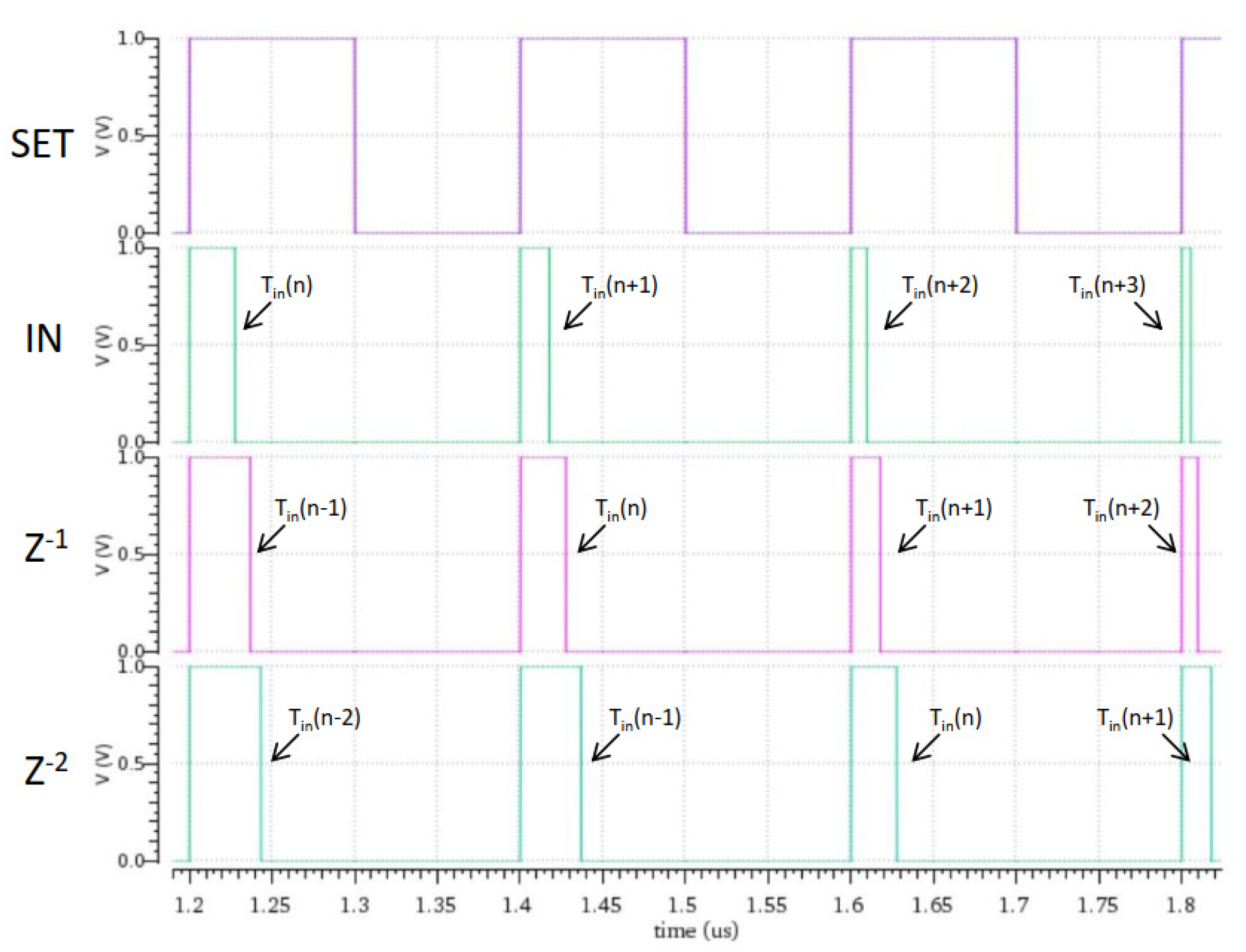
The main goal of this work is to create a z−1 operation. By using n number of z−1 circuits in cascade fashion the z−n operation can be achieved. The Figure 8 displays the simulation results of two cascaded z−1 operators. The input pulses IN with gradually decreased pulse widths pass through two cascaded z−1 operators generating two output signals z−1 and z−2. Comparing the outputs with SET signal it is obvious that the first operator delays the pulses for one cycle when the second does so for two cycles. Using this technique, the pulses of a signal can be delayed by n cycles by using n operators.
6.3. z−1 Accuracy
A metric for the accuracy of the z−1 operation is the time error between the input and output pulse widths, time error = Tin-Tout. The time error should be as small as possible for every input pulse width and for every PT corners after the end of the calibration process. Figure 9 illustrates the time error over PT corners after calibration. The input pulse width Tin ranges between 5 ns and 45 ns. It is obvious that the time error is at acceptable levels with worst-case error around ±33 ps. The time error is less than 0.9% for 40 ns full scale of Tin.
The input pulse widths Tin can theoretically be anywhere between 0 and 50 ns. Using Tin.min = 5 ns or Tin.max = 45 ns, the shorter pulses emerge inside z−1 circuit is 5 ns in both cases, based on the circuit topology. Our approach has a worst-case timing inaccuracy of roughly 33 ps over corners. The Tin.min is around 43.6 dB higher than the worst case time error, according to our findings, which is quite good (20 log (Tin.min/33 ps) = 43.6 dB). If the input pulse width becomes smaller than 5 ns (or larger than 45 ns) the time error increases but the architecture is still functional.
7. Discussion
This work proposes a time-domain z−1 operator based on cascaded time-registers that uses the discharging slope technique. The discharging slope is calibrated over PT variations using a novel digital loop presenting around 5% spread while the time error of the z−1 operation is less than 0.9% for 40 ns input range. Also, the digitally controlled calibration is disabled when the calibration completed cuts down the current consumption. The average current consumption is 30 μA for 5 MHz sampling frequency.
For future work by using z−1 operator, basic arithmetic functions such as adders, subtractors, time amplifiers and integrators can be also implemented. Also, by combining these functions more sophisticated systems can be built and explored, as time-based analog-to-digital converters, digital filters, discrete-time control systems. Also, a very beneficial aspect of this work is that all these types of time-based systems are composed mostly of CMOS digital building blocks and their performance is pretty stable against device size shrinking and low voltage supplies.
Author Contributions
Conceptualization, O.P.-F. and S.V.; methodology, S.V.; validation, O.P.-F.; formal analysis, O.P.-F. and S.V.; investigation, O.P.-F. and S.V.; resources, S.V.; data curation, O.P.-F.; writing—original draft preparation, O.P.-F.; writing—review and editing, S.V.; visualization, O.P.-F. and S.V.; supervision, S.V.; project administration, S.V.; funding acquisition, O.P.-F. and S.V. All authors have read and agreed to the published version of the manuscript.
Funding
This research has been co-financed by the European regional development fund of the European union and Greek national funds through the operational program competitiveness, entrepreneurship and innovation, under the call RESEARCH–CREATE–INNOVATE (project code: T1EDK-02551).
Data Availability Statement
Data sharing not applicable.
Conflicts of Interest
The authors declare no conflict of interest.
References
- Asada, K.; Nakura, T.; Iizuka, T.; Ikeda, M. Time-domain approach for analog circuits in deep sub-micron LSI. IEICE Electron. Express 2018, 15, 20182001. [Google Scholar] [CrossRef] [Green Version]
- Park, Y.J.; Jarrett-Amor, D.; Yuan, F. Time integrator for mixed-mode signal processing. In Proceedings of the 2016 IEEE International Symposium on Circuits and Systems (ISCAS), Montreal, QC, Canada, 22–25 May 2016. [Google Scholar] [CrossRef]
- Staszewski, R.B.; Muhammad, K.; Leipold, D.; Hung, C.M.; Ho, Y.C.; Wallberg, J.L.; Fernando, C.; Maggio, K.; Staszewski, R.; Jung, T.; et al. All-digital TX frequency synthesizer and discrete-time receiver for Bluetooth radio in 130-nm CMOS. IEEE J. Solid-State Circuits 2004, 39, 2278–2291. [Google Scholar] [CrossRef]
- Karmakar, A.; de Smedt, V.; Leroux, P. Pseudo-Differential Time-Domain Integrator Using Charge-Based Time-Domain Circuits. In Proceedings of the 2021 IEEE 12th Latin America Symposium on Circuits and System (LASCAS), Arequipa, Peru, 21–24 February 2021. [Google Scholar] [CrossRef]
- Vlassis, S.; Felouris-Panetas, O.; Souliotis, G.; Plessas, F. Linear Current-to-Time Converter. In Proceedings of the 2019 14th International Conference on Design & Technology of Integrated Systems In Nanoscale Era (DTIS), Mykonos, Greece, 16–18 April 2019. [Google Scholar] [CrossRef]
- Yadav, N.; Kim, Y.; Alashi, M.; Choi, K.K. Sensitive, Linear, Robust Current-To-Time Converter Circuit for Vehicle Automation Application. Electronics 2020, 9, 490. [Google Scholar] [CrossRef] [Green Version]
- Lee, M.; Abidi, A.A. A 9 b, 1.25 ps Resolution Coarse–Fine Time-to-Digital Converter in 90 nm CMOS that Amplifies a Time Residue. IEEE J. Solid-State Circuits 2008, 43, 769–777. [Google Scholar] [CrossRef]
- Oulmane, M.; Roberts, G.W. CMOS Digital Time Amplifiers for High Resolution Timing Measurement. Analog. Integr. Circuits Signal Processing 2005, 43, 269–280. [Google Scholar] [CrossRef]
- Kwon, H.-J.; Lee, J.; Sim, J.-Y.; Park, H.-J. A high-gain wide-input-range time amplifier with an open-loop architecture and a gain equal to current bias ratio. In Proceedings of the IEEE Asian Solid-State Circuits Conference 2011, Jeju, Korea, 14–16 November 2011. [Google Scholar] [CrossRef]
- Kim, D.; Kim, K.; Yu, W.; Cho, S. A Second-Order ΔΣ Time-to-Digital Converter Using Highly Digital Time-Domain Arithmetic Circuits. IEEE Trans. Circuits Syst. II Express Briefs 2019, 66, 1643–1647. [Google Scholar] [CrossRef]
- Ziabakhsh, S.; Gagnon, G.; Roberts, G.W. A Second-Order Bandpass ΔΣ Time-to-Digital Converter with Negative Time-Mode Feedback. IEEE Trans. Circuits Syst. I Regul. Pap. 2019, 66, 1355–1368. [Google Scholar] [CrossRef]
- Zhu, K.; Feng, J.; Lyu, Y.; He, A. High-precision differential time integrator based on time adder. Electron. Lett. 2018, 54, 1268–1270. [Google Scholar] [CrossRef]
- Leene, L.B.; Constandinou, T.G. Time Domain Processing Techniques Using Ring Oscillator-Based Filter Structures. IEEE Trans. Circuits Syst. I Regul. Pap. 2017, 64, 3003–3012. [Google Scholar] [CrossRef]
- Zhu, J.; Nandwana, R.K.; Shu, G.; Elkholy, A.; Kim, S.J.; Hanumolu, P.K. A 0.0021 mm2 1.82 mW 2.2 GHz PLL Using Time-Based Integral Control in 65 nm CMOS. IEEE J. Solid-State Circuits 2017, 52, 8–20. [Google Scholar] [CrossRef]
- Kim, K.; Yu, W.; Cho, S. A 9 bit, 1.12 ps Resolution 2.5 b/Stage Pipelined Time-to-Digital Converter in 65 nm CMOS Using Time-Register. IEEE J. Solid-State Circuits 2014, 49, 1007–1016. [Google Scholar] [CrossRef]
- Orfeas, P.-F.; Vlassis, S. A novel time register with process and temperature calibration. In Proceedings of the 2021 10th International Conference on Modern Circuits and Systems Technologies (MOCAST), Thessaloniki, Greece, 5–7 July 2021. [Google Scholar] [CrossRef]
- Sun, J. Pulse-Width Modulation. Embed. Syst. Program. 2012, 14, 103–104. [Google Scholar] [CrossRef]
Figure 1.
(a) Voltage-to-time conversion using a sample and hold circuit (S/H) and pulse width modulation (PWM), (b) conceptual diagram of a z−1 operator in time domain, (c) basic waveforms of the voltage-to-time conversion and z−1 operation.
Figure 1.
(a) Voltage-to-time conversion using a sample and hold circuit (S/H) and pulse width modulation (PWM), (b) conceptual diagram of a z−1 operator in time domain, (c) basic waveforms of the voltage-to-time conversion and z−1 operation.

Figure 2.
(a) Time register circuit, (b) symbol, (c) fast comparator topology [16] and (d) main waveforms diagram.
Figure 2.
(a) Time register circuit, (b) symbol, (c) fast comparator topology [16] and (d) main waveforms diagram.

Figure 3.
(a) Time-domain z−1 circuit, (b) main waveforms diagram.

Figure 4.
Digital calibration loop for technology process and temperature variation.

Figure 5.
Digitally controlled binary-weighted current mirror.

Figure 6.
Operation of the digital calibration.

Figure 7.
Capacitor voltage Vcap during calibration process.

Figure 8.
Input–output waveforms for z−1 and z−2 operation.

Figure 9.
Time error of a z−1 over different technology process and chip temperature (PT) corners versus pulse width of Tin.
Figure 9.
Time error of a z−1 over different technology process and chip temperature (PT) corners versus pulse width of Tin.


Table 1.
Slope stability over process and temperature corners.
| PT Corner | Calibrated TR Slope (MV/s) | Digital Word (7 bit) | Uncalibrated TR Slope (MV/s) |
|---|---|---|---|
| Typical | 10.306 | 1000001 | 10.010 |
| Cmin_ff_0° | 9.953 | 0110010 | 14.842 |
| Cmin_ff_100° | 9.899 | 0110100 | 12.192 |
| Cmin_ss_0° | 10.286 | 0110101 | 9.786 |
| Cmin_ss_100° | 10.358 | 0111000 | 8.071 |
| Cmax_ff_0° | 9.935 | 1001011 | 10.833 |
| Cmax_ff_100° | 9.858 | 1001110 | 8.448 |
| Cmax_ss_0° | 10.375 | 1010010 | 6.669 |
| Cmax_ss_100° | 10.259 | 1011110 | 5.478 |
Publisher’s Note: MDPI stays neutral with regard to jurisdictional claims in published maps and institutional affiliations. |
© 2022 by the authors. Licensee MDPI, Basel, Switzerland. This article is an open access article distributed under the terms and conditions of the Creative Commons Attribution (CC BY) license (https://creativecommons.org/licenses/by/4.0/).
Share and Cite
MDPI and ACS Style
Panetas-Felouris, O.; Vlassis, S. A Time-Domain z−1 Circuit with Digital Calibration. J. Low Power Electron. Appl. 2022, 12, 3. https://0-doi-org.brum.beds.ac.uk/10.3390/jlpea12010003
AMA Style
Panetas-Felouris O, Vlassis S. A Time-Domain z−1 Circuit with Digital Calibration. Journal of Low Power Electronics and Applications. 2022; 12(1):3. https://0-doi-org.brum.beds.ac.uk/10.3390/jlpea12010003
Chicago/Turabian StylePanetas-Felouris, Orfeas, and Spyridon Vlassis. 2022. "A Time-Domain z−1 Circuit with Digital Calibration" Journal of Low Power Electronics and Applications 12, no. 1: 3. https://0-doi-org.brum.beds.ac.uk/10.3390/jlpea12010003
Note that from the first issue of 2016, this journal uses article numbers instead of page numbers. See further details here.