
Fully Differential Miller Op-Amp with Enhanced Large- and Small-Signal Figures of Merit


 ,
,
Abstract
:1. Introduction
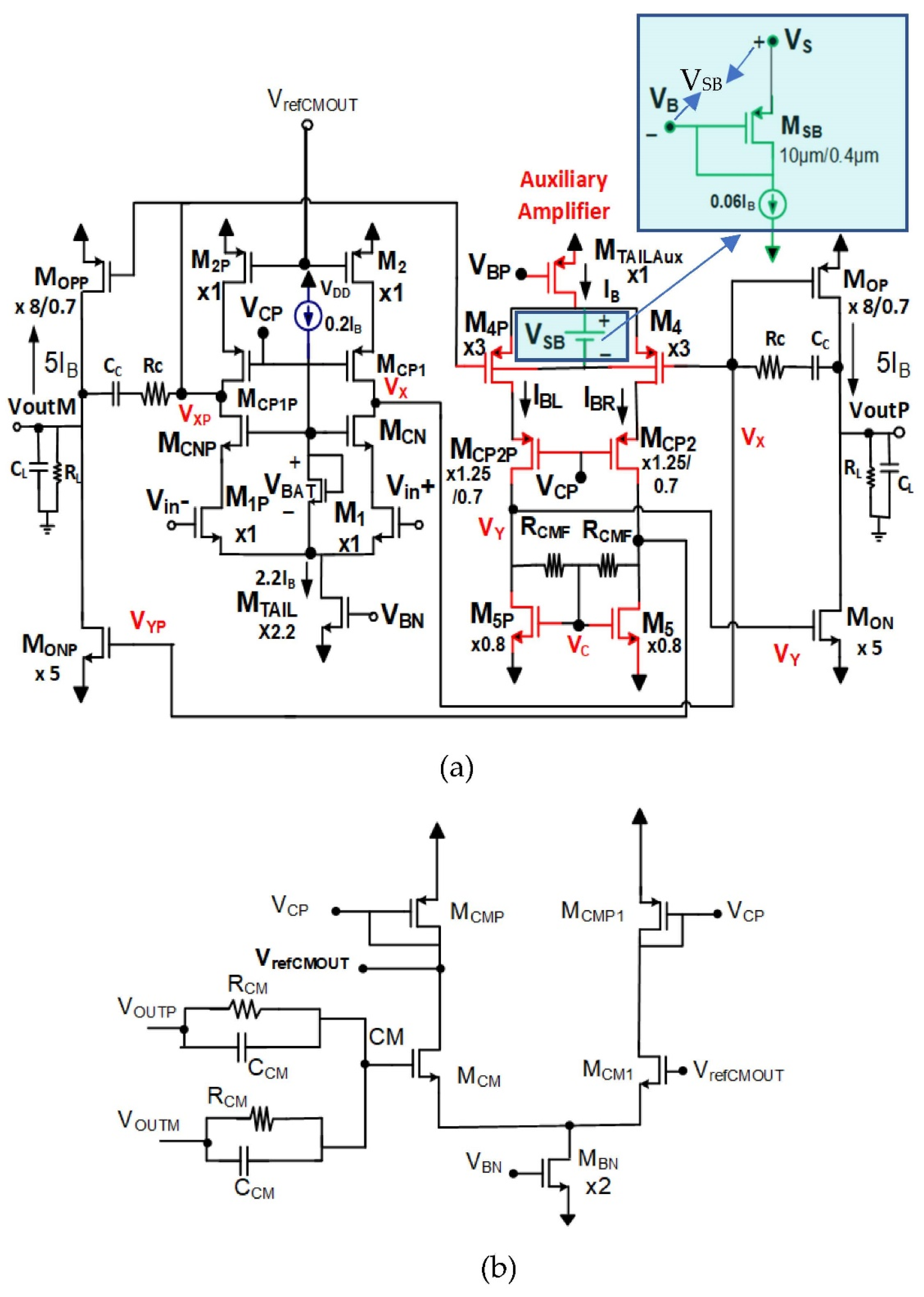
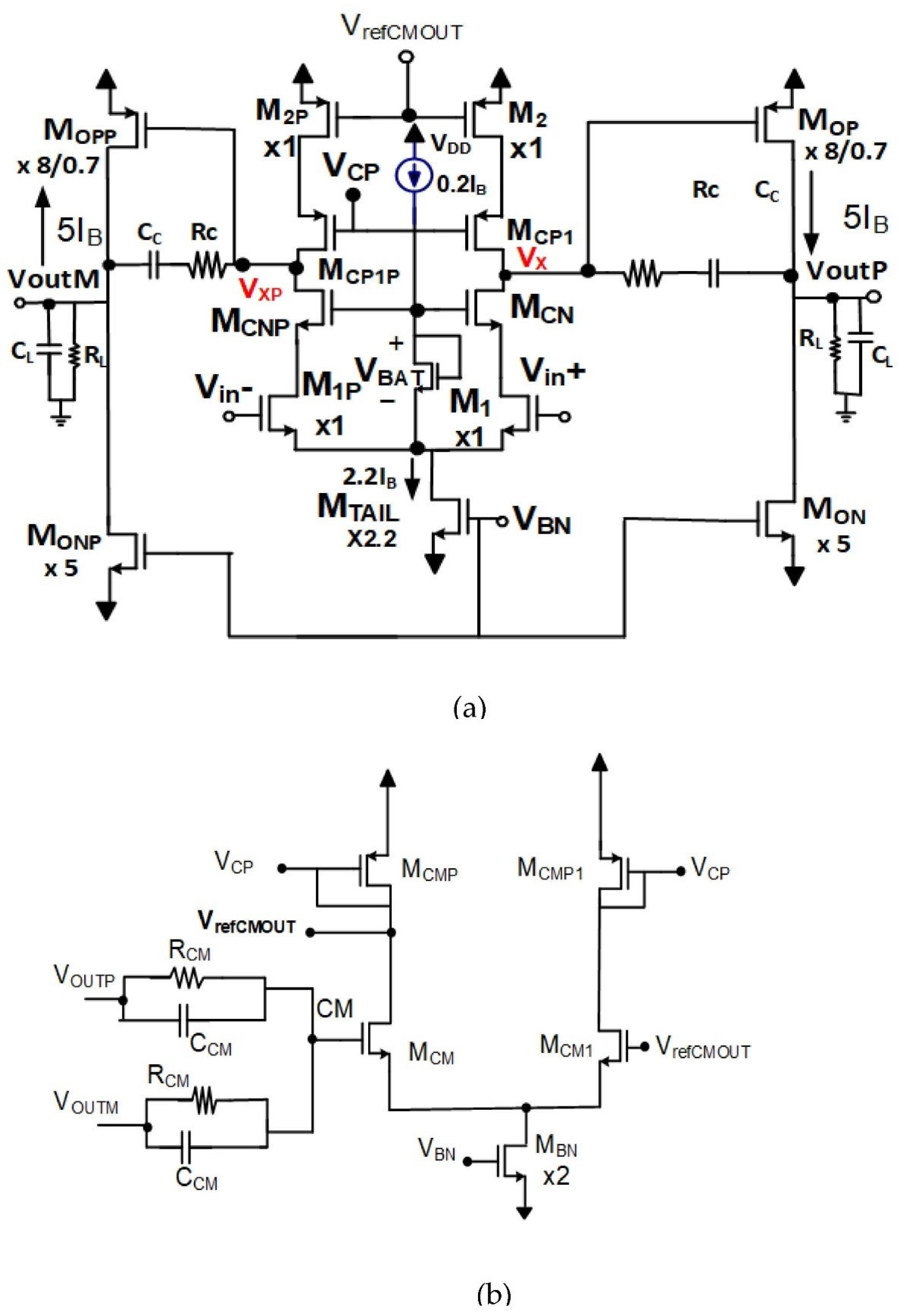
2. Proposed Op-Amp
2.1. Operation
2.2. Frequency Response
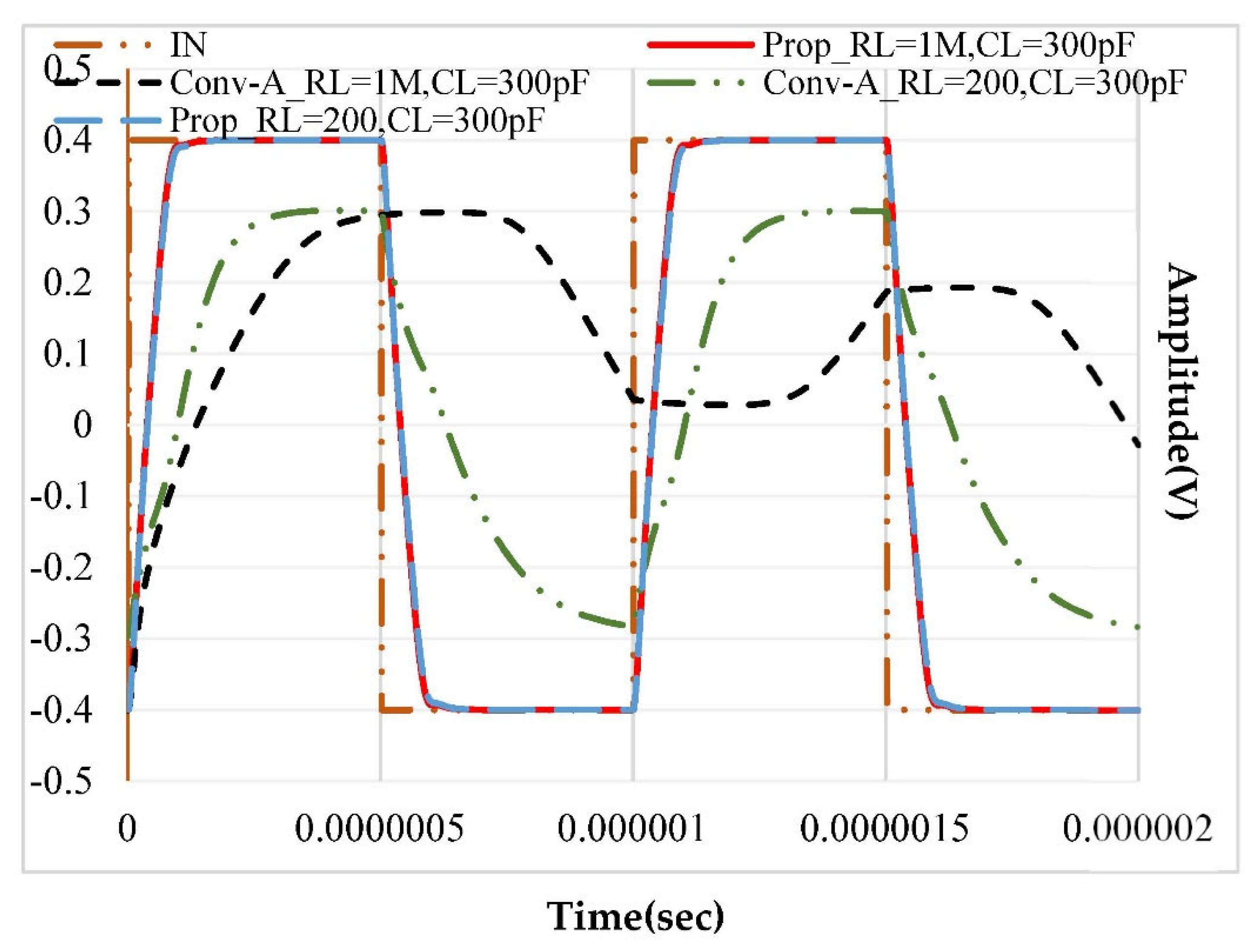
3. Results
4. Conclusions
Author Contributions
Funding
Institutional Review Board Statement
Informed Consent Statement
Data Availability Statement
Conflicts of Interest
References
- Walden, R.H. Analog-to-digital converter survey and analysis. IEEE J. Sel. Areas Commun. 1999, 17, 539–550. [Google Scholar] [CrossRef] [Green Version]
- Karki, J. Fully differential amplifier design in high-speed data acquisition systems. Analog Des. J. 2002. Available online: https://www.ti.com.cn/cn/lit/an/slyt034/slyt034.pdf#page=35 (accessed on 26 December 2021).
- Kobayashi, H.; Kushita, N.; Tran, M.T.; Asami, K.; San, H.; Kuwana, A.; Hatta, A. Analog/Mixed-Signal/RF Circuits for Complex Signal Processing. In Proceedings of the 2019 IEEE 13th International Conference on ASIC (ASICON), Chongqing, China, 29 October–1 November 2019; pp. 1–4. [Google Scholar]
- Gray, P.R.; Hurst, P.J.; Lewis, S.H.; Meyer, R.G. Analysis and Design of Analog Integrated Circuits, 5th ed.; Wiley: Hoboken, NJ, USA, 2001. [Google Scholar]
- Spinelli, E.M.; Haberman, M.A.; Guerrero, F.N.; García, P.A. A High Input Impedance Single-Ended Input to Balanced Differential Output Amplifier. IEEE Trans. Instrum. Meas. 2020, 69, 1682–1689. [Google Scholar] [CrossRef]
- Banu, M.; Khoury, J.M.; Tsividis, Y. Fully differential operational amplifiers with accurate output balancing. IEEE J. Solid-State Circuits 1988, 23, 1410–1414. [Google Scholar] [CrossRef]
- Hassan, A.H.; Mostafa, H.; Salama, K.N.; Soliman, A.M. A Low-Power Time-Domain Comparator for IoT Applications. In Proceedings of the 2018 IEEE 61st International Midwest Symposium on Circuits and Systems (MWSCAS), Windsor, ON, Canada, 5–8 August 2018; pp. 1142–1145. [Google Scholar]
- Razavi, B. Design of Analog CMOS Integrated Circuits, 1st ed.; McGraw-Hill: New York, NY, USA, 2001. [Google Scholar]
- Monticelli, D.M. A quad CMOS single-supply op amp with rail-to-rail output swing. IEEE J. Solid-State Circuits 1986, 21, 1026–1034. [Google Scholar] [CrossRef] [Green Version]
- Langen, K.D.; Huijsing, J.H. Compact low-voltage power-efficient operational amplifier cells for VLSI. IEEE J. Solid-State Circuits 1998, 33, 1482–1496. [Google Scholar] [CrossRef] [Green Version]
- Pang-Cheng, Y.; Jiin-Chuan, W. A class-B output buffer for flat-panel-display column driver. IEEE J. Solid-State Circuits 1999, 34, 116–119. [Google Scholar] [CrossRef]
- Gregorian, R.; Temes, G.C. Analog MOS Integrated Circuits for Signal Processing, 1st ed.; Wiley Series on Filters: Design Manufacturing and Applications; Wiley: Hoboken, NJ, USA, 1986. [Google Scholar]
- Aloisi, W.; Giustolisi, G.; Palumbo, G. A 1-V CMOS output stage with high linearity. In Proceedings of the 2003 International Symposium on Circuits and Systems, 2003. ISCAS’ 03., Bangkok, Thailand, 25–28 May 2003; p. I. [Google Scholar]
- Grasso, A.D.; Palumbo, G.; Pennisi, S. Advances in Reversed Nested Miller Compensation. IEEE Trans. Circuits Syst. I Regul. Pap. 2007, 54, 1459–1470. [Google Scholar] [CrossRef]
- Sutula, S.; Dei, M.; Terés, L.; Serra-Graells, F. Variable-Mirror Amplifier: A New Family of Process-Independent Class-AB Single-Stage OTAs for Low-Power SC Circuits. IEEE Trans. Circuits Syst. I Regul. Pap. 2016, 63, 1101–1110. [Google Scholar] [CrossRef] [Green Version]
- Kuo, P.Y.; Tsai, S.D. An Enhanced Scheme of Multi-Stage Amplifier With High-Speed High-Gain Blocks and Recycling Frequency Cascode Circuitry to Improve Gain-Bandwidth and Slew Rate. IEEE Access 2019, 7, 130820–130829. [Google Scholar] [CrossRef]
- Basumata, U.; Mondal, A.; Das, S.; Rahaman, H. Design of Two-Stage Fully-Differential Driver in SAR ADC with Indirect Feedback Compensation Technique. In Proceedings of the 2021 International Symposium on Devices, Circuits and Systems (ISDCS), Vellore, India, 3–5 March 2021; pp. 1–5. [Google Scholar]
- Ahmed, M.; Shah, I.; Tang, F.; Bermak, A. An improved recycling folded cascode amplifier with gain boosting and phase margin enhancement. In Proceedings of the 2015 IEEE International Symposium on Circuits and Systems (ISCAS), Lisbon, Portugal, 24–27 May 2015; pp. 2473–2476. [Google Scholar]
- Shamsi, H.; Anisheh, S.; Abbasizadeh, H.; Dadkhah, C.; Lee, K.-Y. A 84 dB DC-Gain Two-Stage Class-AB OTA. IET Circuits Devices Syst. 2019, 13, 614–621. [Google Scholar] [CrossRef]
- Neag, M.; Kovács, I.; Oneț, R.; Câmpanu, I. Design options for high-speed OA-based fully differential buffers able to drive large loads. Microelectron. J. 2021, 114, 105115. [Google Scholar] [CrossRef]
- Renteria-Pinon, M.; Ramirez-Angulo, J.; Diaz-Sanchez, A. Simple Scheme for the Implementation of Low Voltage Fully Differential Amplifiers without Output Common-Mode Feedback Network. J. Low Power Electron. Appl. 2020, 10, 34. [Google Scholar] [CrossRef]


| Corner | tt | ff | fs | sf | ss | Std. |
|---|---|---|---|---|---|---|
| ITotalQ (µA) | 253 | 251 | 250 | 249 | 247 | 2 |
| fu (MHz) @ RL =1 MΩ | 15.5 | 16.9 | 15.2 | 14 | 13.5 | 1.19 |
| PM (o) @ RL =1 MΩ | 59 | 56 | 56 | 62 | 63 | 2.92 |
| Gain | 117.9 | 114 | 117.6 | 118 | 117 | 1.5 |
| SR (V/µs) | 13 | 11 | 10 | 10 | 9 | 1.4 |
| Ioutpk−RL =200 Ω (mA) | 2 | 1.9 | 1.9 | 2 | 2 | 0.05 |
| Corner | tt | ff | fs | sf | ss | Std. |
|---|---|---|---|---|---|---|
| ITotalQ (µA) | 253 | 252 | 250 | 252 | 255 | 1.62 |
| fu (MHz) @ RL =1 MΩ | 13.4 | 14.5 | 13 | 13.2 | 12 | 0.8 |
| PM (o) @ RL =1 MΩ | 59 | 58 | 61 | 60 | 60 | 1.01 |
| Gain (dB) | 116.4 | 110 | 113 | 114.2 | 120 | 3.35 |
| SR (V/µs) | 13 | 12 | 11 | 12 | 14 | 1.01 |
| Ioutpk− RL =200 Ω (mA) | 2 | 1.9 | 2 | 2 | 2 | 0.04 |
| Corner | tt | ff | fs | sf | ss | Std. |
|---|---|---|---|---|---|---|
| ITotalQ (µA) | 251 | 259 | 251 | 252 | 255 | 3.07 |
| fu (MHz) @ RL = 1 MΩ | 9.5 | 9.4 | 9.5 | 10 | 9.2 | 0.26 |
| PM (o) @ RL = 1 MΩ | 58 | 58 | 58 | 57 | 59 | 0.63 |
| Gain (dB) | 100 | 95 | 111 | 110 | 117 | 7.9 |
| SR (V/µs) | 11 | 14 | 11 | 12 | 15 | 1.62 |
| Ioutpk−RL =200 Ω (mA) | 2 | 1.8 | 1.9 | 2 | 2 | 0.08 |
| Parameter (Units) | Proposed | Conv-A | [17] | [18] | [19] | [20] | [21] |
|---|---|---|---|---|---|---|---|
| Inversion Level | SI | SI | SI | SI | SI | SI | SB |
| CMOS Process (µm) | 0.18 | 0.18 | 0.18 | 0.18 | 0.18 | 0.35 | 0.18 |
| Supply Voltage (V) | ±0.9 | ±0.9 | 1.8 | 1.8 | 1.8 | 3.3 | ±300 |
| Capacitive Load (pF) | 5–300 | 5–300 | 10 | 1 | 100 | 25 | 10 |
| Resistive Load (Ω) | 1 M/200 | 1 M/200 | - | - | - | 500 | - |
| SR (V/μs) | 13 | 0.9 | 17.83 | 650 | 63 | 248.6 | 8.4 |
| DC Gain (dB) | 116.4/ 74.5 | 96.8/57.4 | 73 | 85.6 | 84 | 69.5 | 42.2 |
| PM (º) | 59/82 @CL = 300 pF, RL = 1 MΩ/ @CL = 300 pF, RL = 200 Ω | 57/90 | 64 | 66.7 | 77 | 69.65 | 54 |
| fu (MHz) | 13.32/11.21 | 3.88/4.2 | 15 | 987 | 91 | 354 | 16.1 |
| CMRR @DC (dB) | 96 | 90 | 80 | 80 | - | 45 | 85.12 |
| PSRR+ @DC (dB) | 95 | 87 | 78 | 78 | - | 27.5 | 53.25 |
| PSRR-@DC (dB) | 92 | 85 | - | - | - | 56.89 | |
| Ioutpk + RL (µA) | 2000 @200 Ω | 1500 @200 Ω | - | - | - | 2000 @500 Ω | - |
| Ioutpk−RL =200 Ω (µA) | 2000 | 1500 | - | - | - | 0 | - |
| ItotQ (µA) | 253 | 182 | 239 | 1000 | 1722 | 8042 | 41.3 |
| Power (μW) | 455 | 327.6 | 429.68 | 1800 | 3100 | 26,540 | 24.8 |
| Input Referred Noise | 317@1 kHz nV/√Hz | 330@1 KHz nV/√Hz | 84@100 kHz nV/√Hz | 118 µVrms (1 Hz–100 MHz) | 340@100 kHz nV/√Hz | 35.52 @100 kHz | 69@1 MHz |
| FOMCEDyn (V.pF/µs.µW) | 8.6 | 0.82 | 0.41 | 0.4 | 2 | 0.23 | 3.39 |
| FOMSS (MHz.pF/µW) | 8.7/7.3 | 3.5/3.8 | 0.35 | 0.5 | 2.9 | 0.33 | 6.49 |
| FOMCEStat (µA/µW) | 7.9 | - | - | - | - | 0.08 | - |
Publisher’s Note: MDPI stays neutral with regard to jurisdictional claims in published maps and institutional affiliations. |
© 2022 by the authors. Licensee MDPI, Basel, Switzerland. This article is an open access article distributed under the terms and conditions of the Creative Commons Attribution (CC BY) license (https://creativecommons.org/licenses/by/4.0/).
Share and Cite
Paul, A.; Ramirez-Angulo, J.; Vázquez-Leal, H.; Huerta-Chua, J.; Diaz-Sanchez, A. Fully Differential Miller Op-Amp with Enhanced Large- and Small-Signal Figures of Merit. J. Low Power Electron. Appl. 2022, 12, 9. https://0-doi-org.brum.beds.ac.uk/10.3390/jlpea12010009
Paul A, Ramirez-Angulo J, Vázquez-Leal H, Huerta-Chua J, Diaz-Sanchez A. Fully Differential Miller Op-Amp with Enhanced Large- and Small-Signal Figures of Merit. Journal of Low Power Electronics and Applications. 2022; 12(1):9. https://0-doi-org.brum.beds.ac.uk/10.3390/jlpea12010009
Chicago/Turabian StylePaul, Anindita, Jaime Ramirez-Angulo, Héctor Vázquez-Leal, Jesús Huerta-Chua, and Alejandro Diaz-Sanchez. 2022. "Fully Differential Miller Op-Amp with Enhanced Large- and Small-Signal Figures of Merit" Journal of Low Power Electronics and Applications 12, no. 1: 9. https://0-doi-org.brum.beds.ac.uk/10.3390/jlpea12010009