Analysis of Threshold Voltage Flexibility in Ultrathin-BOX SOI FinFETs †


Abstract
:1. Introduction
2. Experimental
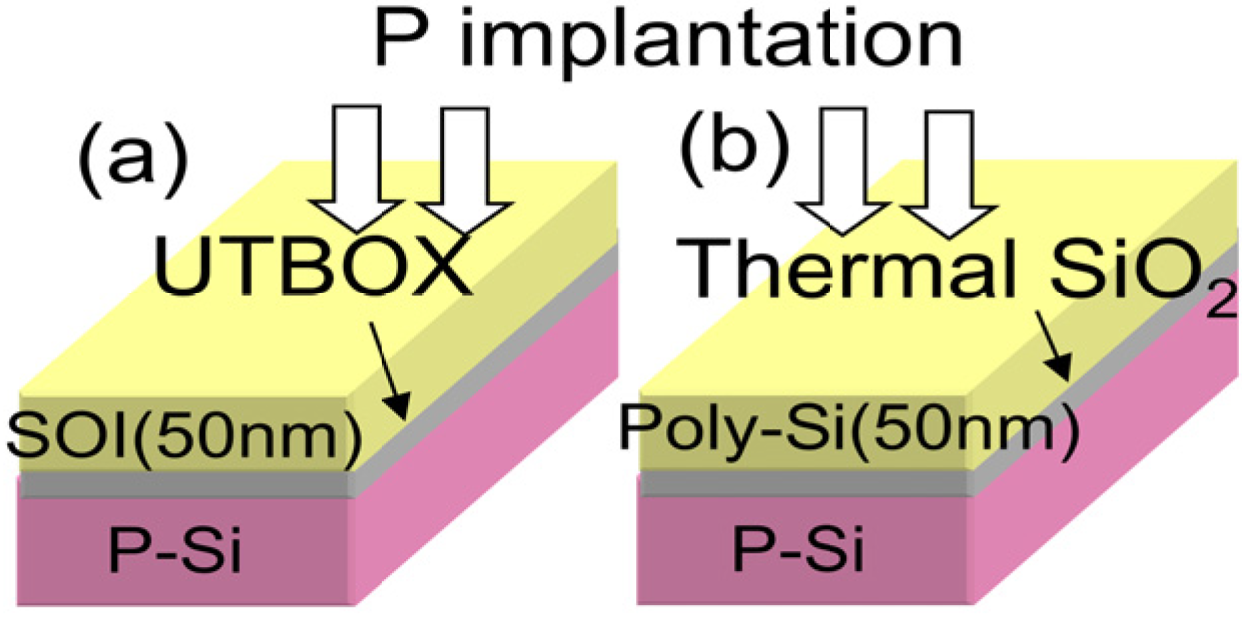
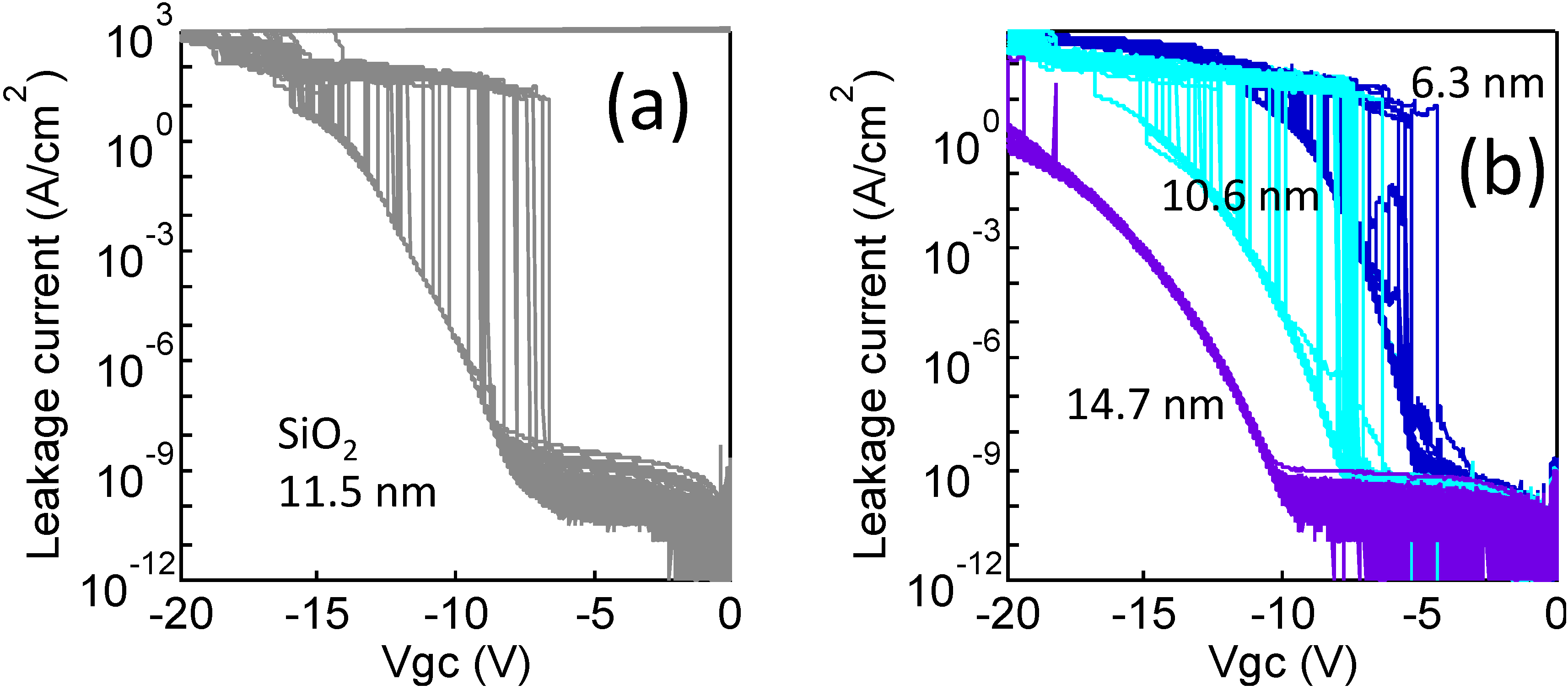
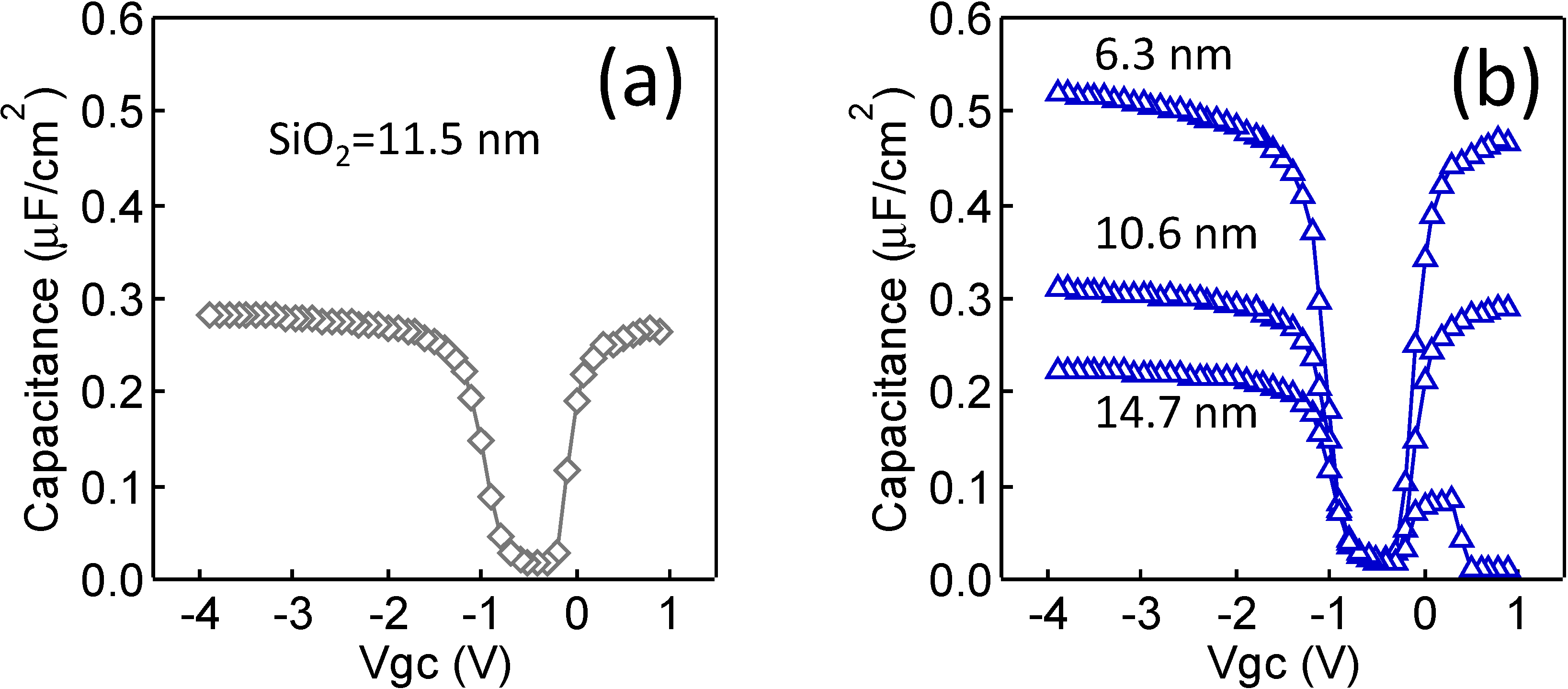
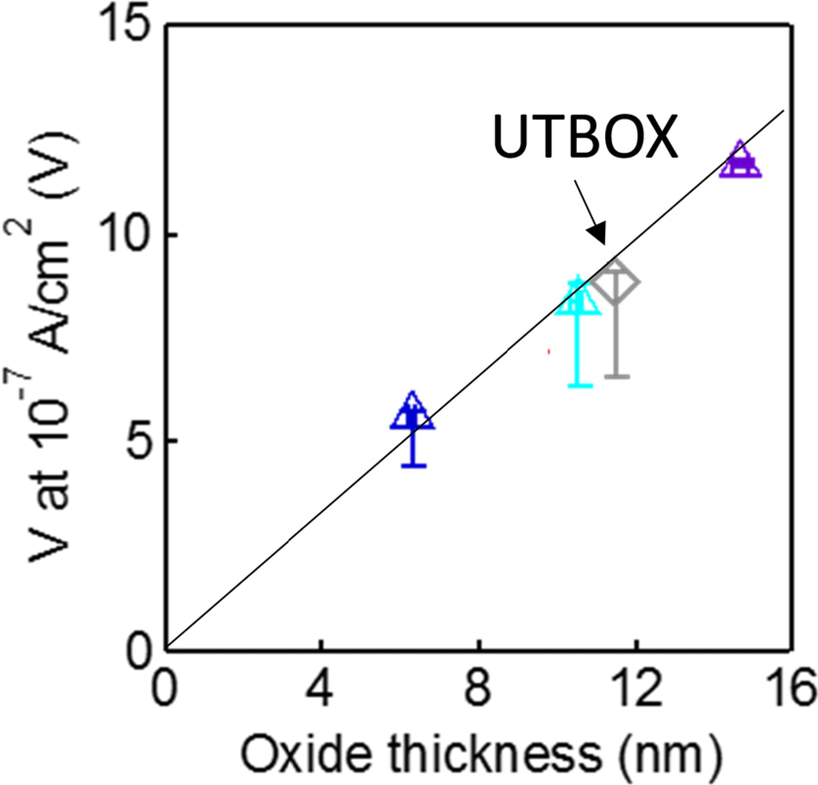
2.1. MOS Capacitor

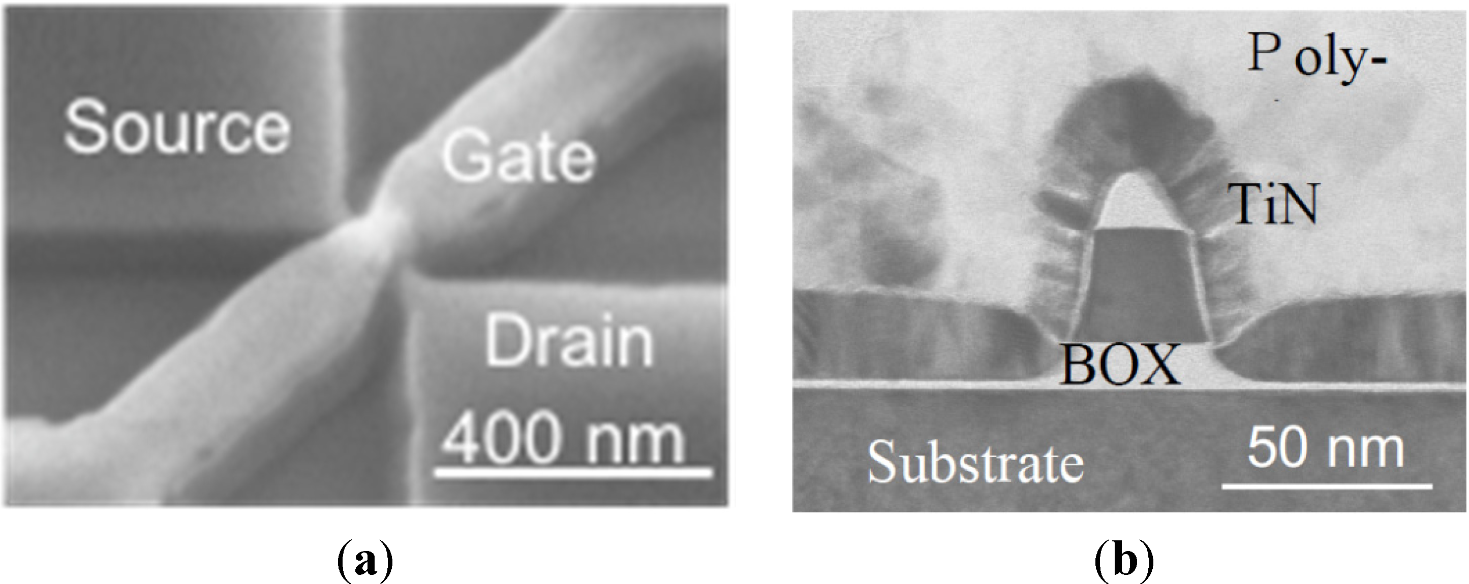
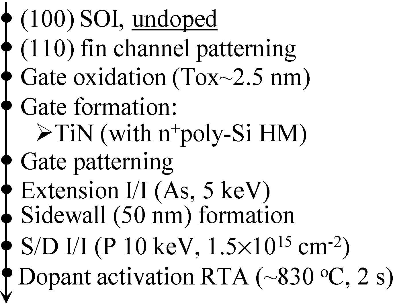
2.2. Device Fabrication

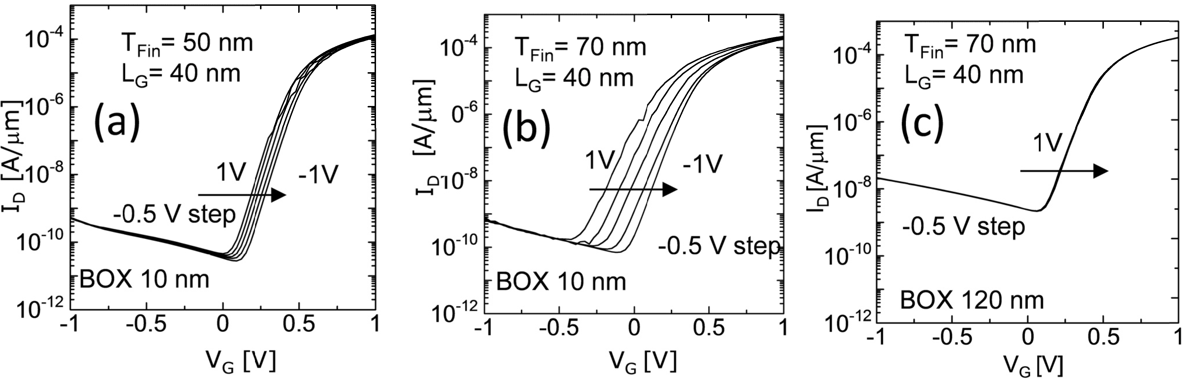
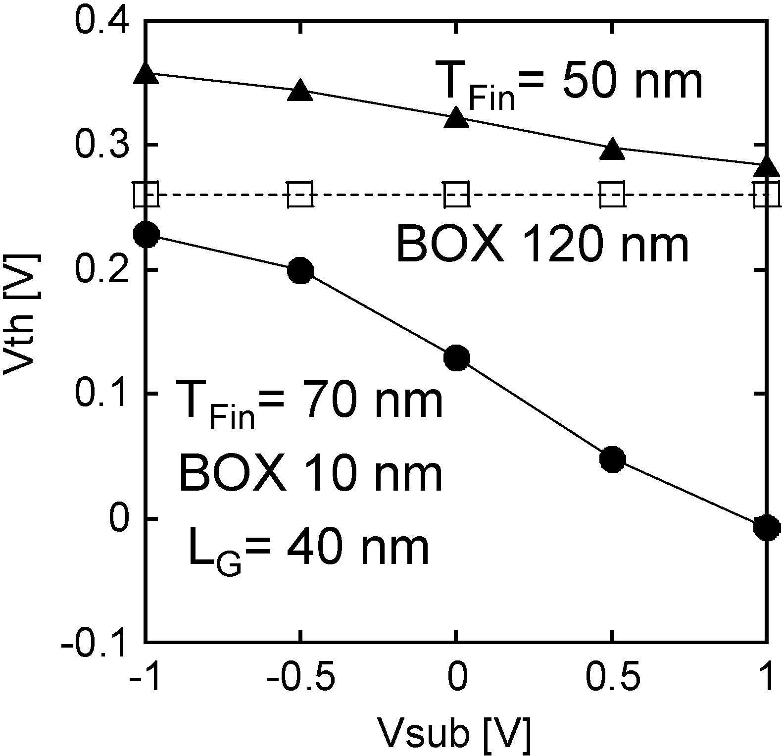
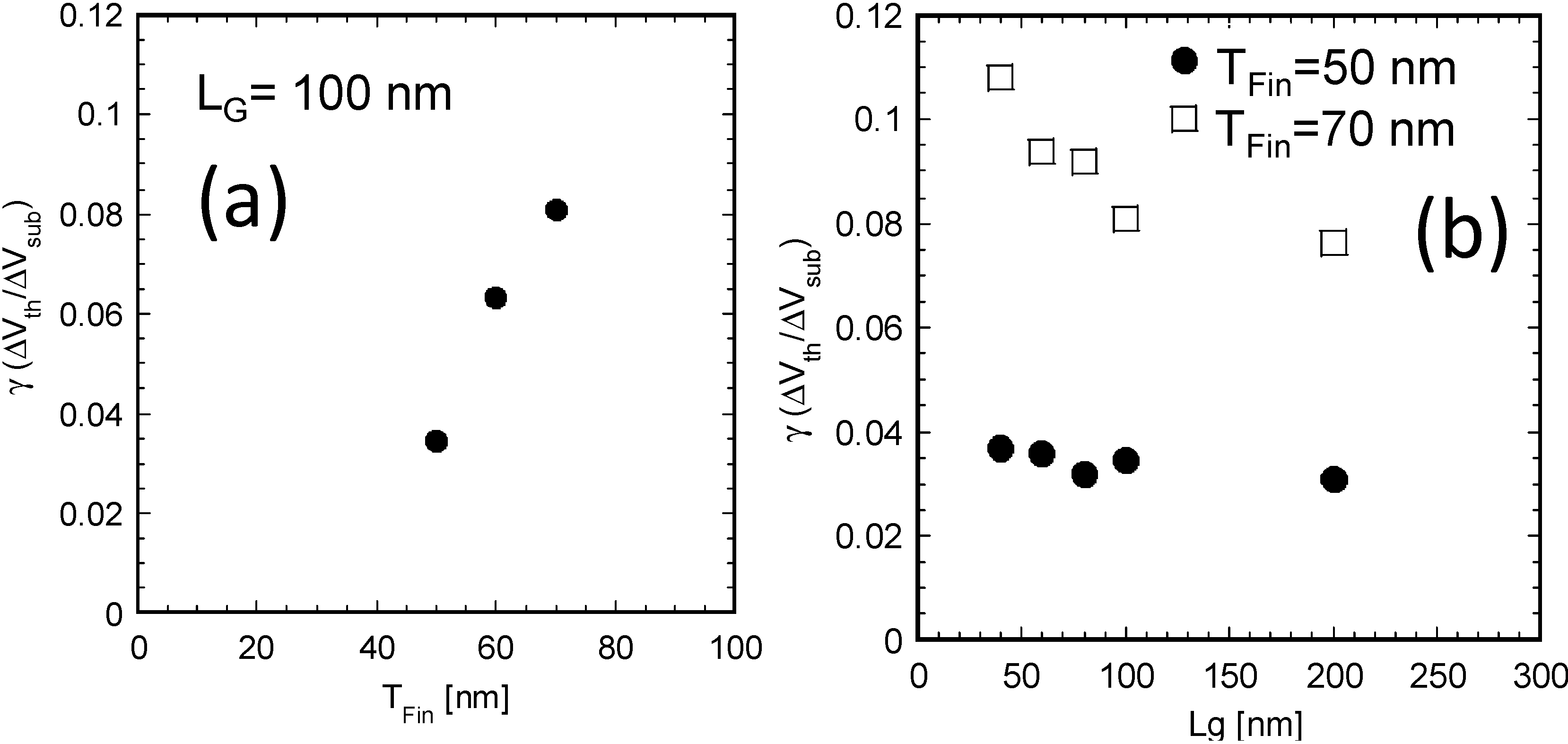
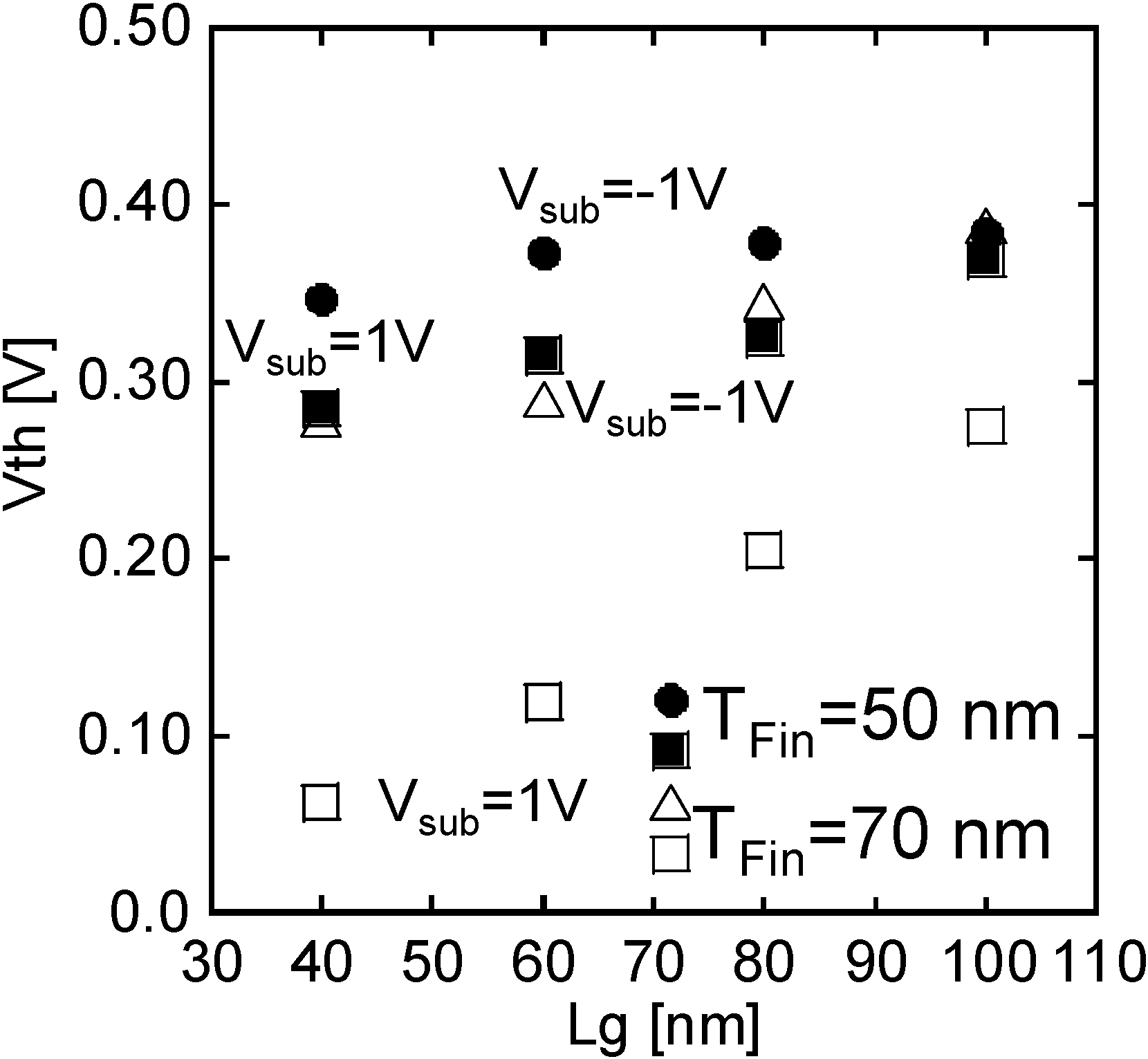
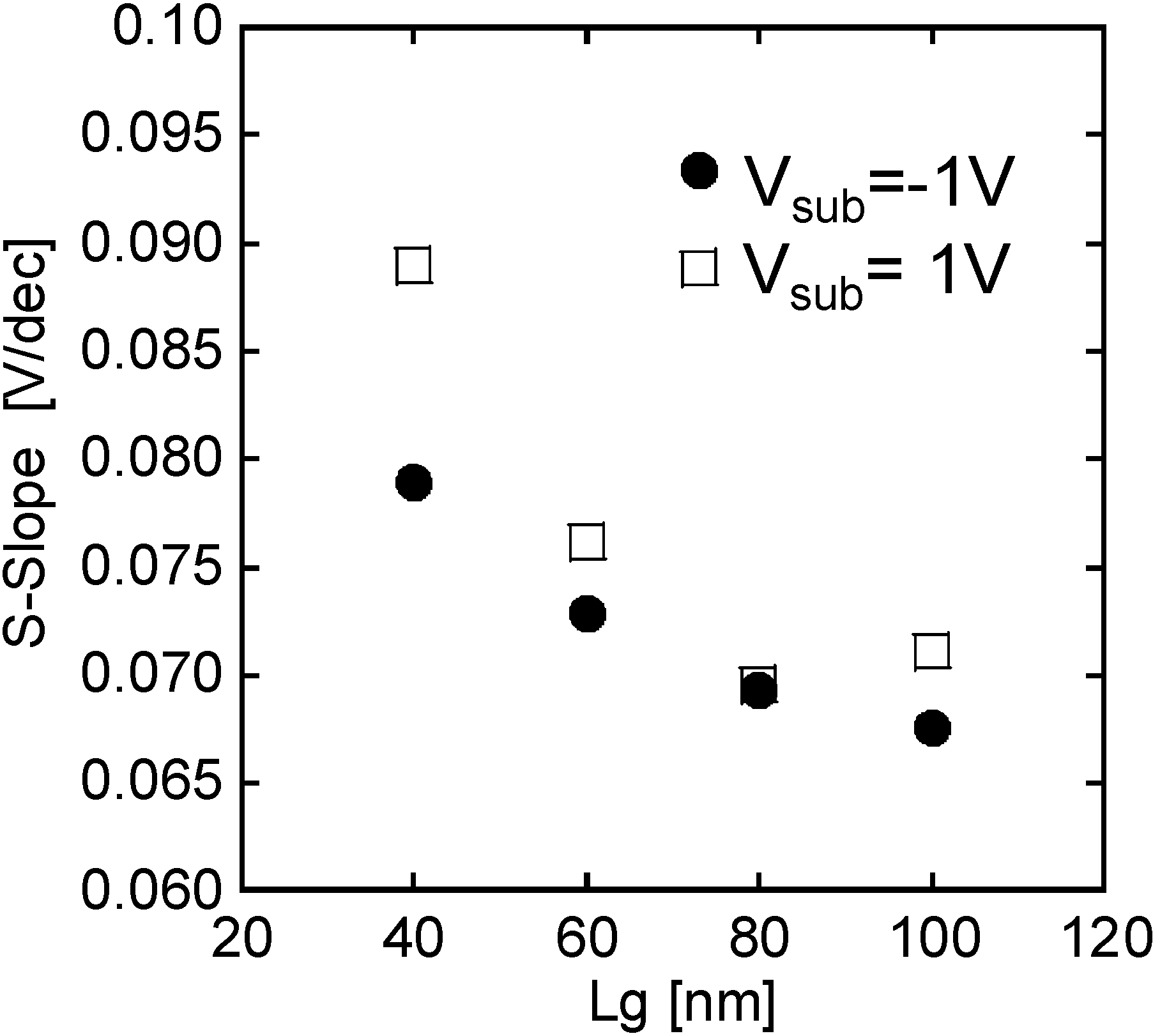
3. Results and Discussion


4. Conclusions
Author Contributions
Conflicts of Interest
References
- Yan, R.-H.; Ourmazd, A.; Lee, K. Scaling the Si MOSFET: From Bulk to SOI to Bulk. IEEE Trans. Electron Devices 1992, 39, 1704–1710. [Google Scholar] [CrossRef]
- Yong, K. Short-Channel Effect in Fully Depleted SOI MOSFET’s. IEEE Trans. Electron Devices 1989, 36, 399–402. [Google Scholar] [CrossRef]
- Mizuno, T.; Okamura, J.; Toriumi, A. Experimental study of threshold voltage fluctuations using an 8K MOSFET array. In Proceedings of the 1993 Symposium on VLSI Technology, Kyoto, Japan, 17–19 May 1993; pp. 41–42.
- Sekigawa, T.; Hayashi, Y. Calculated threshold-voltage characteristics of an XMOS transistor having an additional bottom gate. Solid State Electron 1984, 27, 827–828. [Google Scholar] [CrossRef]
- Hisamoto, D.; Lee, W.-C.; Kedzierski, J.; Takeuchi, H.; Asano, K.; Kuo, C.; Anderson, E.; King, T.-J.; Bokor, J.; Hu, C. FinFET-a self-aligned double-gate MOSFET scalable to 20-nm. IEEE Trans. Electron Devices 2000, 47, 2320–2325. [Google Scholar] [CrossRef]
- Matsukawa, T.; Endo, K.; Liu, Y.X.; O’uchi, S.; Ishikawa, Y.; Yamauchi, H.; Tsukada, J.; Ishii, K.; Sakamoto, K.; Suzuki, E.; et al. Dual Metal Gate FinFET Integration by Ta/Mo Diffusion Technology for Vt Reduction and Multi-Vt CMOS Application. Solid-State Electron. 2009, 53, 701–705. [Google Scholar] [CrossRef]
- Xiong, S.; Bokor, J. Sensitivity of Double-Gate and FinFET Devices to Process Variations. IEEE Trans. Electron Devices 2003, 50, 2255–2261. [Google Scholar] [CrossRef]
- Chian, M.H.; Lin, J.-N.; Kim, K.; Chuang, C.-T. Random Dopant Fluctuation in Limited-Width FinFET Technologies. IEEE Trans. Electron Devices 2007, 54, 2055–2059. [Google Scholar] [CrossRef]
- Nagumo, T.; Hiramoto, T. Design Guideline of Multi-Gate MOSFET with Substrate-Bias Control. IEEE Trans. Electron Devices 2006, 53, 3025–3031. [Google Scholar] [CrossRef]
- Park, S.J.; Jeon, D.-Y.; Montès, L.; Barraud, S.; Kim, G.-T.; Ghibaudo, G. Impact of channel width on back biasing effect in tri-gate MOSFET. Microelectron. Eng. 2014, 114, 91–97. [Google Scholar] [CrossRef]
- Ohtou, T.; Hiramoto, T.; Saraya, T. Variable-Body-Factor SOI MOSFET with Ultrathin Buried Oxide for Adaptive Threshold Voltage and Leakage Control. IEEE Trans. Electron. Devices 2008, 55, 40–47. [Google Scholar] [CrossRef]
- Ohtou, T.; Nagumo, T.; Hiramoto, T. Variable Body Effect Factor Fully Depleted Silicon-On-Insulator Metal Oxide Semiconductor Field Effect Transistor for Ultra Low-Power Variable-Threshold-Voltage Complementary Metal Oxide Semiconductor Applications. Jpn. J. Appl. Phys. Part 1 2004, 43, 3311–3314. [Google Scholar] [CrossRef]
- Tsuchiya, R.; Horiuchi, M.; Kimura, S.; Yamaoka, M.; Kawahara, T.; Maegawa, S.; Ipposhi, T.; Ohji, Y.; Matsuoka, H. Silicon on thin BOX: A new paradigm of the CMOSFET for low-power high-performance application featuring wide-range back-bias control. In Proceedings of the IEEE International Electron Devices Meeting, San Francisco, CA, USA, 13–15 December 2004; pp. 631–634.
- Majumdar, A.; Ren, Z.; Koester, S.J.; Haensch, W. Undoped-Body Extremely Thin SOI MOSFETs with Back Gates. IEEE Trans. Electron. Devices 2009, 56, 2270–2276. [Google Scholar] [CrossRef]
- Endo, K.; Migita, S.; Ishikawa, Y.; Liu, Y.; Matsukawa, T.; O’uchi, S.; Tsukada, J.; Mizubayashi, W.; Morita, Y.; Ota, H.; et al. Flexible Vth FinFETs with 9-nm-Thick Extremely-Thin BOX. In Proceedings of the IEEE SOI Conference, Napa, CA, USA, 1–4 October 2012.
- Endo, K.; Ishikawa, Y.; Liu, Y.; Matsukawa, T.; O’uchi, S.; Tsukada, J.; Migita, S.; Mizubayashi, W.; Morita, Y.; Ota, H.; et al. Analysis of Vth Flexibility in Ultrathin-BOX SOI FinFETs. In Proceedings of the IEEE S3S Conference, Monterey, CA, USA, 7–10 October 2013.
- Liu, Y.; Masahara, M.; Ishii, K.; Sekigawa, T.; Takashima, H.; Yamauchi, H.; Suzuki, E. A highly Vth-controllable 4T FinFET with an 8.5-nm-thick Si-fin channel. IEEE Electron Device Lett. 2004, 25, 510–512. [Google Scholar] [CrossRef]
- Endo, K.; Masahara, M.; Liu, Y.X.; Ishii, T.M.K.; Sugimata, E.; Takashima, H.; Yamauchi, H.; Suzuki, E. Investigation of N-Channel Triple-Gate Metal-Oxide-Semiconductor Field-Effect Transistors on (100) Silicon On Insulator Substrate. Jpn. J. Appl. Phys. 2006, 45, 3097–3100. [Google Scholar] [CrossRef]
- Ota, K.; Saitoh, M.; Tanaka, C.; Numata, T. Systematic Study of Back-Gate Bias Effects in Ultrathin-BOX Tri-gate (UTBT) Transistor with 10nm-Diameter Nanowire Channel. In Proceedings of the Solid State Device and Materials, Kyoto, Japan, 25–27 September 2012.
© 2014 by the authors; licensee MDPI, Basel, Switzerland. This article is an open access article distributed under the terms and conditions of the Creative Commons Attribution license (http://creativecommons.org/licenses/by/3.0/).
Share and Cite
Endo, K.; Migita, S.; Ishikawa, Y.; Matsukawa, T.; O'uchi, S.-i.; Tsukada, J.; Mizubayashi, W.; Morita, Y.; Ota, H.; Yamauchi, H.; et al. Analysis of Threshold Voltage Flexibility in Ultrathin-BOX SOI FinFETs. J. Low Power Electron. Appl. 2014, 4, 110-118. https://0-doi-org.brum.beds.ac.uk/10.3390/jlpea4020110
Endo K, Migita S, Ishikawa Y, Matsukawa T, O'uchi S-i, Tsukada J, Mizubayashi W, Morita Y, Ota H, Yamauchi H, et al. Analysis of Threshold Voltage Flexibility in Ultrathin-BOX SOI FinFETs. Journal of Low Power Electronics and Applications. 2014; 4(2):110-118. https://0-doi-org.brum.beds.ac.uk/10.3390/jlpea4020110
Chicago/Turabian StyleEndo, Kazuhiko, Shinji Migita, Yuki Ishikawa, Takashi Matsukawa, Shin-ichi O'uchi, Junji Tsukada, Wataru Mizubayashi, Yukinori Morita, Hiroyuki Ota, Hitomi Yamauchi, and et al. 2014. "Analysis of Threshold Voltage Flexibility in Ultrathin-BOX SOI FinFETs" Journal of Low Power Electronics and Applications 4, no. 2: 110-118. https://0-doi-org.brum.beds.ac.uk/10.3390/jlpea4020110