Article

MOS Current Mode Logic Near Threshold Circuits †

Department of Electrical Engineering, University of Rochester, Rochester, NY 14627, USA
*
Author to whom correspondence should be addressed.
This is an extended version of the “Performance Characteristics of 14 nm Near Threshold MCML Circuits” paper that was presented at the IEEE S3S Conference 2013.
J. Low Power Electron. Appl. 2014, 4(2), 138-152; https://0-doi-org.brum.beds.ac.uk/10.3390/jlpea4020138
Submission received: 6 March 2014 / Revised: 29 April 2014 / Accepted: 15 May 2014 / Published: 11 June 2014
(This article belongs to the Special Issue Selected Papers from IEEE S3S Conference 2013)

Abstract

:
Near threshold circuits (NTC) are an attractive and promising technology that provides significant power savings with some delay penalty. The combination of NTC technology with MOS current mode logic (MCML) is examined in this work. By combining MCML with NTC, the constant power consumption of MCML is reduced to leakage power levels that can be tolerated in certain modern applications. Additionally, the speed of NTC is improved due to the high speed nature of MCML technology. A 14 nm Fin field effect transistor (FinFET) technology is used to evaluate these combined circuit techniques. A 32-bit Kogge Stone adder is chosen as a demonstration vehicle for feasibility analysis. MCML with NTC is shown to yield enhanced power efficiency when operated above 1 GHz with a 100% activity factor as compared to standard CMOS. MCML with NTC is more power efficient than standard CMOS beyond 9 GHz over a wide range of activity factors. MCML with NTC also exhibits significantly lower noise levels as compared to standard CMOS. The results of the analysis demonstrate that pairing NTC and MCML is efficient when operating at high frequencies and activity factors.

1. Introduction

In the era of handheld mobile devices, the performance of integrated circuits is a primary concern. Power consumption and speed are two primary characteristics of high performance integrated circuits [1]. In this work, both of these characteristics are addressed by utilizing low power near threshold circuits (NTC) [2] in combination with high speed MOS current mode logic (MCML) [3]. In recent years, NTC has become an increasingly popular approach to lower power consumption at the expense of decreased speed. The quadratic reduction in power consumption is accomplished by operating near the threshold voltage. A similar reduction in supply voltage, however, results in a ten times reduced speed of near threshold circuits as compared to circuits operating at the nominal supply voltage. In contrast, MCML utilizes a differential circuit topology driven by a constant tail current and is generally characterized by high speed and high power consumption. The combination of MCML with NTC produces a balanced circuit methodology that compensates for the vulnerable aspects while benefiting from the advantages of each technology.
The paper is structured as follows. In Section 2, NTC and MCML are introduced. The benefits of combining MCML with NTC are described in Section 3. The simulation environment is reviewed in Section 4, and the results are summarized in Section 5. Some conclusions are offered in Section 6.

2. Background

Combining MOS current mode logic with near threshold circuits is proposed in this work. Each technology is individually described in this section to provide a basis for the combination presented in Section 3. Near threshold circuits are discussed in Section 2.1, and MCML is described in Section 2.2.

2.1. Near Threshold Circuits
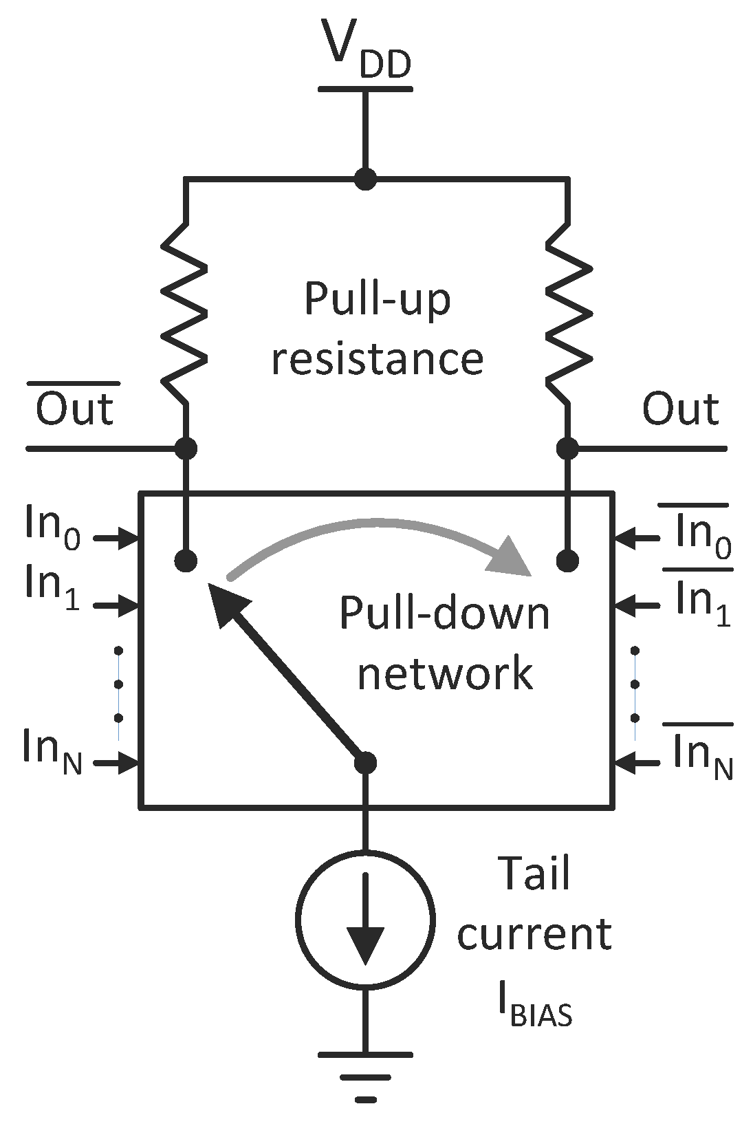
Near threshold circuits consume an order of magnitude less power than circuits operating under nominal voltages while not suffering from the significant delay penalty found in subthreshold circuits. NTC has therefore become an attractive methodology for sub-30 nm CMOS circuits [4]. By operating near the threshold voltage (as compared to a much lower voltage deep within the subthreshold region), near threshold circuits represent a balanced approach to tackling the power issue, while maintaining circuit delays within a reasonable range. This concept is illustrated in Figure 1. In this figure, NTC is compared to two opposite extremes. At one extreme, subthreshold circuits represent minimal energy consumption coupled with slow speed operation. At the other extreme, nominal circuits consume significant energy coupled with fast speed of operation. With respect to these extrema, circuits operating in the near threshold region consume only two times more energy as compared to the subthreshold region while remaining energy efficient (ten times less than nominal voltage operation [5]). Alternatively, circuits operating in the near threshold region exhibit ten times longer delays as compared to circuits operating in the nominal voltage region. The delay of circuits operating in the subthreshold region can be a hundred to a thousand times greater than NTC [5].
Figure 1. Energy and delay in different operating regions.
Jlpea 04 00138 g001
The primary difficulty of operating near the threshold voltage is the increased sensitivity to process, voltage, and temperature variations (PVT). Small variations in supply voltage can greatly affect the operating point (speed and power consumption) of NTC. Power noise in the range of 50 to 100 mV can shift the operating point from above the threshold voltage to below the threshold voltage, essentially pushing NTC either to subthreshold or above threshold operation. Alternatively, the threshold voltage of a circuit can shift due to process variations, leading to the same effect, operating a circuit either in the subthreshold region or above the threshold voltage. This behavior can lead to large shifts in gate driving capabilities of NTC transistors due to the exponential dependence of gate current on supply and threshold voltages [6]. Additionally, the low power characteristics of NTC degrade when the supply voltage is above the threshold voltage. This increased sensitivity, however, can be mitigated using the techniques discussed in Section 3.

2.2. MCML Circuits

MCML is the CMOS counterpart of bipolar emitter coupled logic (ECL), which has been in use in high speed applications since the 1970s. MCML maintains the benefits of traditional ECL, such as high speed, reduction in d I / d t noise, and common mode noise rejection, without requiring bipolar transistors [7].
An ideal MCML gate is shown in Figure 2. The gate is composed of three parts: the pull-up load resistors, the pull-down logic network, and a constant current source. The pull-up load resistors are typically PMOS transistors, as depicted in Figure 3 for an MCML universal gate. PMOS transistors are used in the pull-up network, similar to standard CMOS. During the low-to-high transition, the PMOS pull-up network charges the output to V D D , unlike NMOS, which charges the output to V D D - V t h .
Figure 2. Ideal MOS current mode logic (MCML) gate modeled with resistive loads and a tail current.
Jlpea 04 00138 g002
Figure 3. Basic MCML gates that share an asymmetric universal MCML gate topology: (a) MCML NAND gate; and (b) MCML NOR gate. The PMOS pull-up gate voltage, V p b i a s , is typically connected to ground. The gate voltage, V n b i a s , drives the NMOS transistor, providing the tail current.
Jlpea 04 00138 g003
The pull-down network is fully differential and generates both the true and complementary forms of the output signal; consequently, the logic can often be simplified by eliminating inverters. The constant current source is provided by a single NMOS transistor and typically uses a separate control voltage, V n b i a s . This constant current is steered between the differential branches (i.e., the pull-up loads) to change the outputs, while the total current from V D D to ground is ideally maintained as constant.

2.2.1. Power Efficiency of MCML

The power consumed by an MCML gate is
P M C M L = I B I A S × V D D .
Note that the power consumed by an MCML gate does not depend on the operating frequency. In other words, an MCML gate consumes constant current (and power) from the power supply network independent of the logic activity or frequency. This behavior is in contrast to the C V 2 f power dissipated by conventional CMOS, where the power consumed by a static CMOS gate exhibits a linear relationship with operating frequency. MCML is therefore more power efficient at high frequencies than static CMOS. Standard MCML circuits operating under nominal conditions exhibit enhanced power efficiency at frequencies above 5 GHz. At these frequencies, MCML, although more power efficient than standard CMOS above 5 GHz, suffers from high power densities not acceptable in modern ultra-mobile microprocessors. To reduce the frequency at which MCML dissipates less power than static CMOS, MCML circuits are operated near the threshold voltage, as suggested in this paper. By combining MCML with NTC technology, the frequency at which MCML dissipates less power than standard CMOS can be lowered to around 1 GHz, as shown in Figure 8.

2.2.2. High Speed of MCML

MOS current mode logic operates at frequencies significantly higher than standard CMOS. These frequencies are achieved due to the low delay of MCML. This property of MCML circuits is largely due to the reduced voltage swing of MCML gates. The voltage swing of an MCML gate is commonly two to ten times lower than V D D , resulting in higher circuit speeds as compared to standard CMOS [8].

2.2.3. Low Noise Environment of MCML
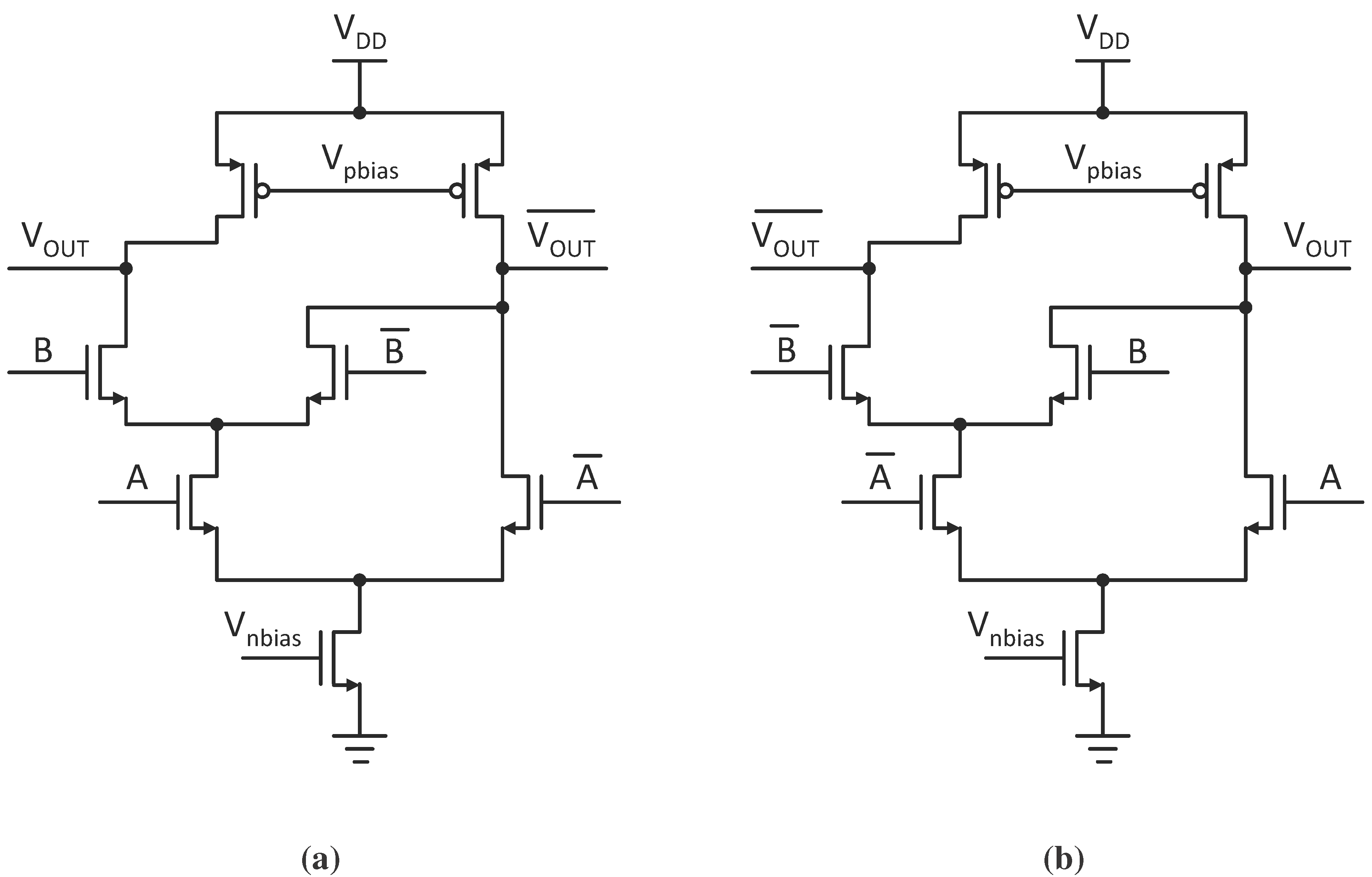
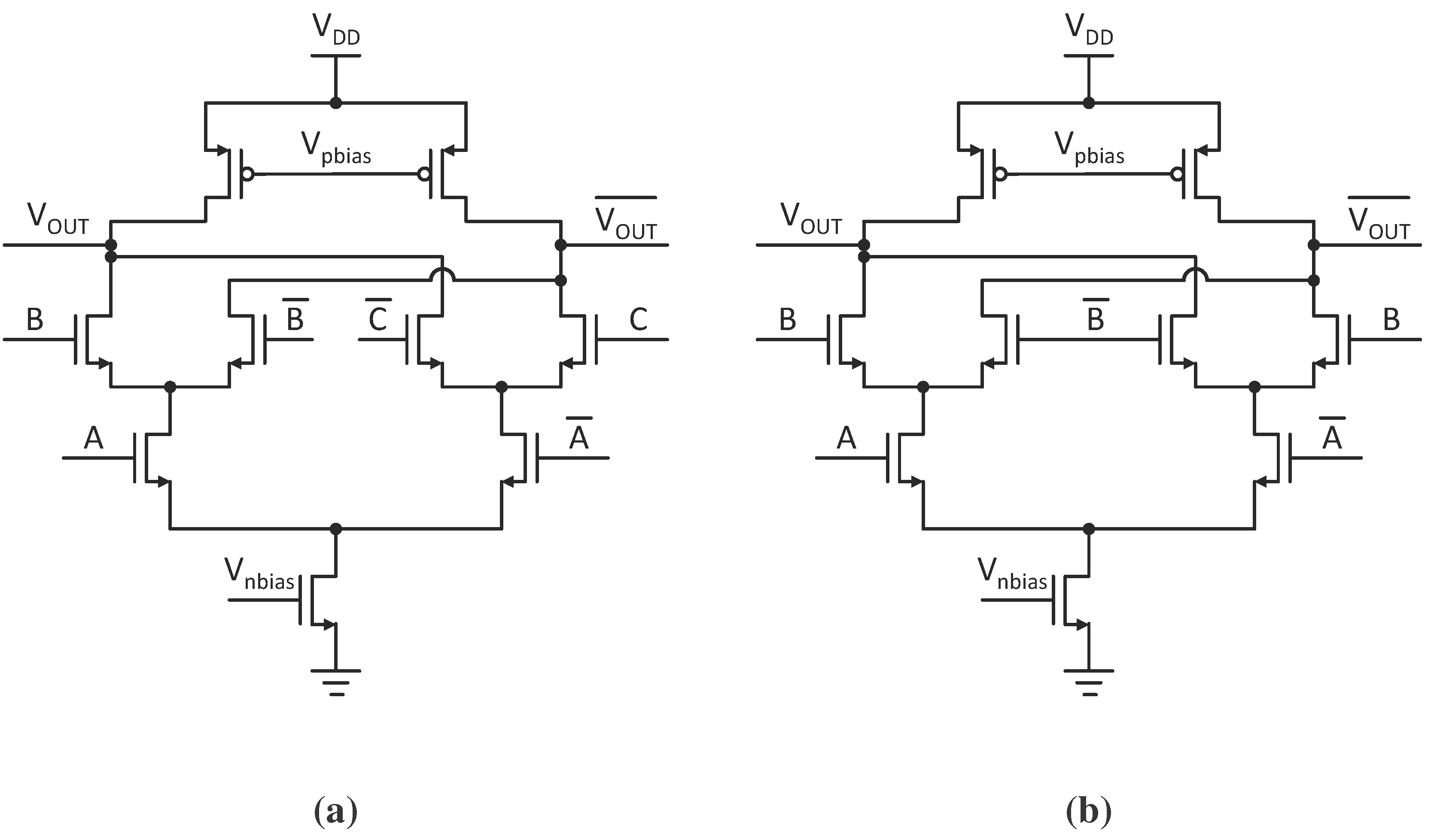
CMOS circuits suffer from simultaneous switching noise (SSN), a significant source of on-chip noise [9]. In contrast, the near constant current of MCML (regardless of the state, i.e., idle, transition, or active) produces significantly less on-chip SSN. The low noise of MCML is particularly relevant when combined with NTC due to the exponential sensitivity of NTC circuits to the power supply when operating near the threshold voltage [5]. In this paper, the simultaneous switching noise generated by MCML NTC circuits is shown to be ten times less noise than in standard CMOS with NTC circuits. A noise analysis of these circuits is described in Section 5.2.

2.2.4. Logic Gates

The design process of MCML circuits is more complex than standard CMOS. Circuit parameters, such as the supply voltage, voltage swing, pull-up equivalent resistance, tail current, and input network, need to be considered. These parameters are correlated. A change in one parameter leads to adjustments in the other parameters. For example, the voltage that determines the low output is a function of both the supply voltage and voltage swing of the gate. The voltage swing affects the pull-up resistance and tail current. If the tail current is chosen for a low power operating point, the voltage swing is affected if the pull-up resistance is not modified. This behavior is in contrast to standard CMOS gates, which have fewer design parameters (e.g., supply voltage, transistor sizes, and threshold voltage) , and each parameter independently affects the operating point. The use of high threshold voltage transistors rather than standard transistors to set a low power operating point does not change the output swing of the gate.
To overcome this limitation of MCML technology, a family of logic gates has been designed based on universal MCML gates [10]. This approach standardizes and simplifies the process of MCML logic design to a small number of universal gates. This capability is possible because basic MCML gates (i.e., NAND, AND, NOR, and OR) only differ in the input and output connections. These basic MCML gates share a common circuit topology, also referred to as a universal gate structure. This universal gate structure can be either symmetric or asymmetric, depending upon the set of gates that use this universal gate structure, as well as power, speed, and area constraints. The asymmetric universal gate structure of NAND and NOR gates is illustrated in Figure 3 [1,10]. As shown in this figure, the only difference between these gates are the input and output connections. The lack of symmetry in this universal gate structure leads to asymmetric rise and fall times. An asymmetric universal gate structure, however, has two fewer input transistors and wires.
This set of basic gates can be further expanded to include an XOR gate if a symmetric topology is considered. An MCML XOR gate is shown in Figure 4b to illustrate a symmetric universal gate structure [1]. Other basic gate types (such as NAND, AND, NOR, and OR) use this symmetric universal gate topology with modified input and output connections. The drawback of a symmetric universal gate is the increased area. A symmetric universal gate structure exhibits symmetric rise and fall transitions and is simpler to design due to the symmetry of the circuit structure. The symmetry enables the use of equally sized transistors in both the left and right branches of the logic gate, eliminating the need to balance the branch currents.

3. Combination of MCML and NTC

A novel approach for combining MCML with NTC is presented in this section. The combination of MCML with NTC is proposed to exploit the mutual benefits and to offset the drawbacks of each technology. This combination is presented in Section 3.1. In Section 3.2, the sensitivity to PVT variations of MCML with NTC is discussed. The characterization of basic gates is presented in Section 3.3.

3.1. MCML with NTC

The reason for combining MCML with NTC is as follows. Standard CMOS with NTC consumes less power when operated near the threshold voltage, as discussed in Section 2.1. This low voltage operation, however, is responsible for the slower speed, as compared to the same circuit operating at a nominal supply voltage. Alternatively, MCML circuits consume greater power as compared to standard CMOS, due to the static current, as described in Section 2.2. The differential nature of MCML gates, however, requires a smaller voltage swing at the output, which significantly reduces the gate delay. CMOS with NTC therefore dissipates less power, but operates at a lower speed, while standard MCML technology provides enhanced speed, but consumes a constant high power during both active and idle periods.
Figure 4. Symmetric universal MCML gate structure used as a topology for basic MCML gates: (a) Symmetric universal MCML gate; and (b) MCML XOR gate. The PMOS pull-up gate voltage, V p b i a s , is typically connected to ground. The gate voltage, V n b i a s , drives the NMOS transistor, providing the tail current.
Jlpea 04 00138 g004
MCML and NTC uncombined therefore either dissipate excessive power or are too slow. When combined, the constant power consumption of MCML is reduced to much lower levels, producing an effective circuit topology. Additionally, the low noise advantages of MCML, as described in Section 2.2, are maintained in the combined circuit topology.
One issue, however, remains partly unresolved by this combination: the high sensitivity of MCML NTC to PVT variations. This difficulty is discussed with greater detail in Section 3.2.
The advantages and disadvantages of combining both circuit approaches are summarized in Table 1. In this table, as discussed in Section 2.1, Section 2.2, and Section 3, the speed of MCML with NTC is comparable to the speed of standard CMOS. The energy is approximately one order of magnitude less than standard CMOS; however, the same energy is consumed during idle periods. The simultaneous switching noise induced on the power network is up to two orders of magnitude lower, than standard CMOS, and is one order of magnitude lower than in CMOS with NTC. Finally, MCML with NTC is primarily sensitive to V t h mismatch among the PMOS pull-up transistors; however, the sensitivity can be reduced using the techniques described in this section.
Table 1. Combination of NTC and MCML.
Standard CMOSCMOS with NTCStandard MCMLMCML with NTC
SpeedS S / 10 Up to 10 × S Up to S
Energy consumptionE E / 10 E (also when idle) E / 10 (also when idle)
Power network inductive noise 10 × N NN N / 10
VariationsStandard sensitivity V t h variations can cause
timing failures
Sensitivity to mismatch V t h mismatch can cause
logical failures

3.2. Sensitivity to Process Variation of MCML with NTC

There are three aspects to this issue, voltage variations, process mismatch, and temperature variations. MCML circuits provide lower SSN noise, which reduces voltage variations by about ten times, as compared to standard CMOS. This low noise environment significantly limits fluctuations near the threshold voltage, reducing variations caused by sensitivity to noise. MCML can suffer from process mismatch between the two differential branches. The PMOS pull-ups, however, are located in close proximity, allowing the transistors to be aligned to alleviate this effect [11,12]. Additionally, process variations can adversely affect the threshold voltage of the PMOS transistors within the pull-up network. This effect, however, is significantly reduced in sub-20 nm FinFET technologies due to the light doping of the transistor channel and improved gate control [13]. Finally, local temperature variations have minimal effect on the differential branches due to the physical proximity and the aforementioned layout techniques.
A Monte Carlo analysis is used to demonstrate the effect of process mismatch on MCML with NTC. In this analysis, a universal MCML with NTC gate is characterized with 1000 iterations. For each iteration, the threshold voltage of the pull-up PMOS transistors in the gate is assigned with an independently generated and normally distributed value; resulting in process mismatch between threshold voltages of up to 41 mV, which is equal to approximately 11% of nominal threshold voltage. The analyzed MCML with NTC gate exhibited correct logic values and did not fail under mismatch of up to 11%. Histograms of delay and power are presented, respectively, in Figure 5a and Figure 5b.
Figure 5. Monte Carlo simulation of MCML with NTC gate: (a) Delay variation; and (b) Variation of power consumption. The mean delay is μ = 110 ps with σ = 24 ps, while the mean power is μ = 827 nW with σ = 2.8 nW.
Jlpea 04 00138 g005

3.3. Characterization of Basic MCML with NTC Gates

The basic gates described in Section 2.2 are characterized in terms of power consumption and delay, as summarized in Table 2. The combination of MCML with NTC exhibits promising characteristics at the gate level. For basic gates, the combination of MCML with NTC exhibits lower delay, achieving higher operating frequencies as compared to standard CMOS with NTC. Additionally, the dynamic power dissipated by MCML gates operating near the threshold voltage is significantly lower than the dynamic power dissipated by standard CMOS gates operating near the threshold voltage. As described in Section 2.2, however, MCML technology exhibits the same power dissipation during idle periods, which is significantly higher than the static power of standard CMOS. This behavior is less significant for the combination of MCML and NTC when operating at high frequencies where the idle time is less, as described in Section 5.
Table 2. Performance comparison of basic logic gates using standard CMOS with NTC, and MCML with NTC.
Gate typeTechnologyDelay (ps)Dynamic power (nW)Static power (nW)Supply voltage (mV)
NAND gateCMOS with NTC1202,2700.150400
MCML with NTC99800800400
NOR gateCMOS with NTC1121,6000.090400
MCML with NTC891,2001,200400
XOR gateCMOS with NTC2672,6001.225400
MCML with NTC147800800400

4. Simulation Setup

In this section, standard CMOS circuits and MCML-based NTC circuits are compared. The analysis is based on 14 nm low power (LP) FinFET predictive technology models [14]. A standard threshold voltage of V t h = 350 mV is assumed. The supply voltage is set to 400 mV to operate near the threshold voltage with an MCML voltage swing of 100 mV. A Kogge Stone adder is used to evaluate this proposed circuit topology and is described in Subsection 4.1. Power and noise simulation setups are described, respectively, in Subsection 4.2 and Subsection 4.3.

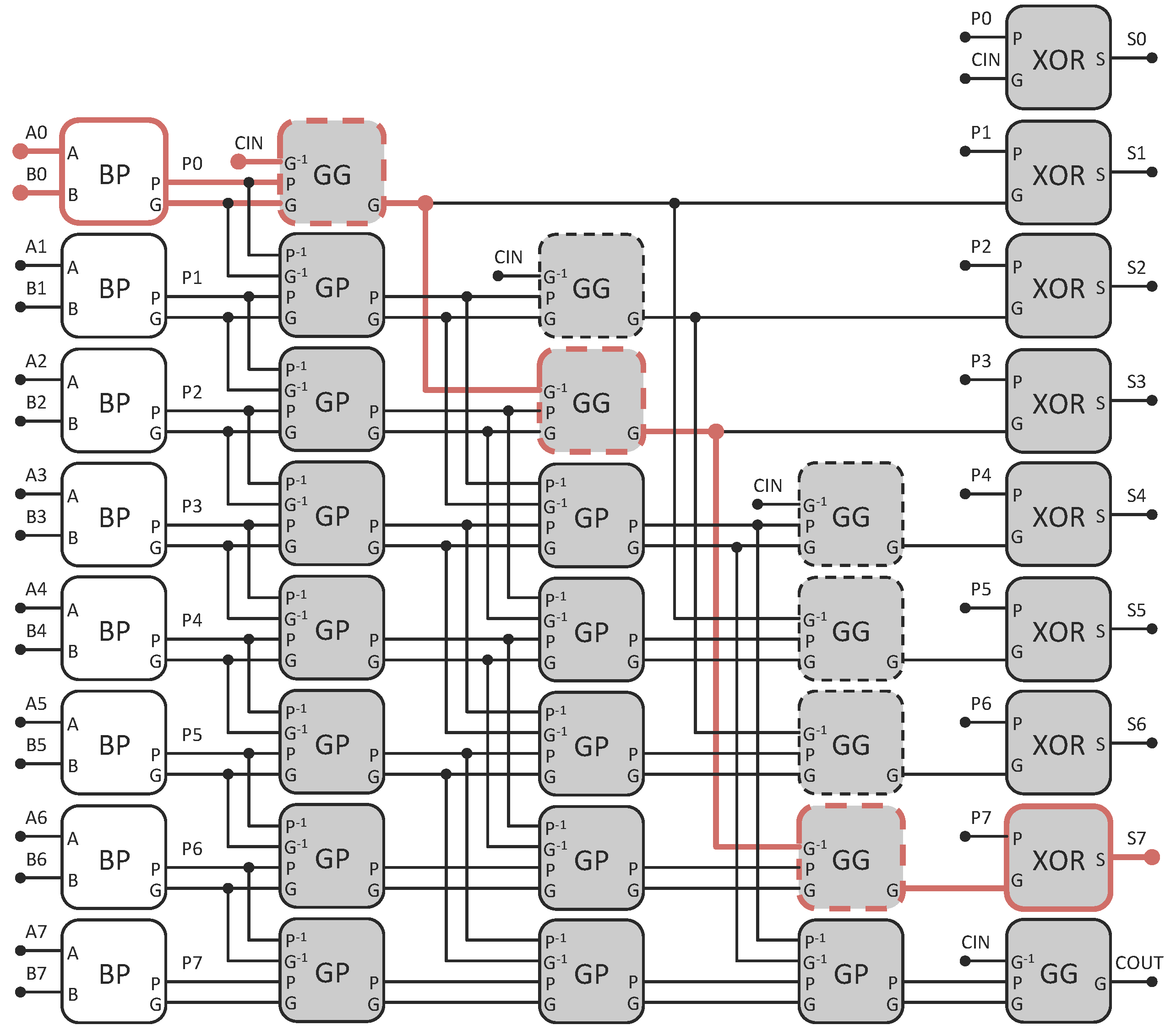
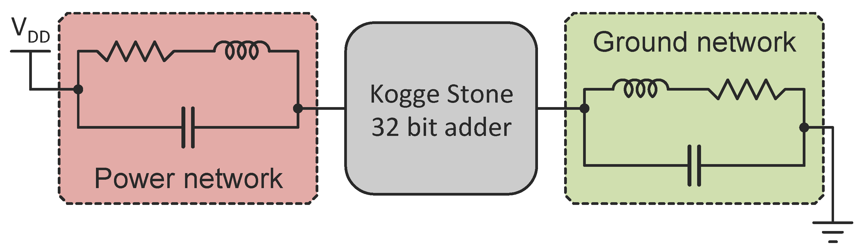
4.1. Description of Test Circuit

A 32-bit Kogge Stone adder [15] is evaluated in both standard CMOS, and MCML with NTC. The Kogge Stone adder is a parallel carry look ahead adder [15]. The choice of a 32-bit Kogge Stone adder as a test circuit is due to the high speed nature of this circuit topology. The structure of the 32-bit test circuit is demonstrated with an 8-bit Kogge Stone adder, as presented in Figure 6. The 8-bit Kogge Stone adder has the same periodic structure as the 32-bit adder. The adder is composed of three building blocks: bit propagate, group generate, and group propagate cells, with a 32-bit input and 32-bit output. The critical delay path is highlighted in red, as shown in Figure 6. This critical path is used for evaluating the worst case delay to determine the maximum operating frequency of the circuit. Two versions of a 32-bit Kogge Stone adder are compared. One version is based on MCML with NTC logic, while the other version is based on CMOS with NTC logic.

4.2. Power Simulation Setup

The power versus frequency characteristics of the Kogge Stone adder are illustrated in Figure 8. Both MCML and standard CMOS circuits are stimulated with the same 32-bit input with a duty cycle equivalent to 1 GHz. The input with the longest propagation delay, T D , sets the maximum possible operating frequency F m a x = 1 / T D of the circuit. The different power consumption levels are dependent on the supply voltage for standard CMOS, varying from subthreshold operation (200 mV) to nominal voltage (800 mV). For MCML NTC circuits, however, the power consumption is primarily dependent on the tail current. The power consumption is the average with different inputs, and consists of both dynamic and static power consumption. The dynamic power consumption is the average power consumed by the test circuits during a signal transition. The static power consumption is the average power consumed during the remaining portion of the input cycle when the logic is idle. Note that the static power consumption is a key difference between standard CMOS and MCML. Therefore, to produce a fair comparison, standard CMOS is compared to MCML with activity factors of 10%, 20%, and 100%. These activity factors represent a wide range of circuits, from active each cycle (e.g., clock distribution signals) to active only every tenth cycle (common data paths).
Figure 6. Eight-bit Kogge Stone adder within a 32-bit Kogge Stone adder. The white blocks represent the bit propagate (BP) cells, solid gray blocks represent the group propagate (GP) cells, and doted gray blocks represent the group generate (GG) cells. The critical delay path is highlighted by a bold red line.
Jlpea 04 00138 g006
For standard CMOS, frequencies above 9 GHz cannot be achieved with minimum sized gates in 14 nm FinFET CMOS. The exponential increase in the power consumed by standard CMOS beyond 9 GHz is caused by the increased size of the gates with a nominal voltage supply of 1 volt. For MCML with NTC, the supply voltage is set constant near a threshold voltage of 400 mV.

4.3. Noise Simulation Setup

The same circuit structure is used to analyze the noise induced within the power network. An equivalent lump model of the power network is illustrated in Figure 7. The resistive, capacitive, and inductive impedances are based on the international technology roadmap for semiconductors (ITRS) guidelines [16]. The results are discussed in Section 5.
Figure 7. Test circuit with a lumped impedance model for evaluating noise in power and ground networks.
Jlpea 04 00138 g007

5. Simulation Results
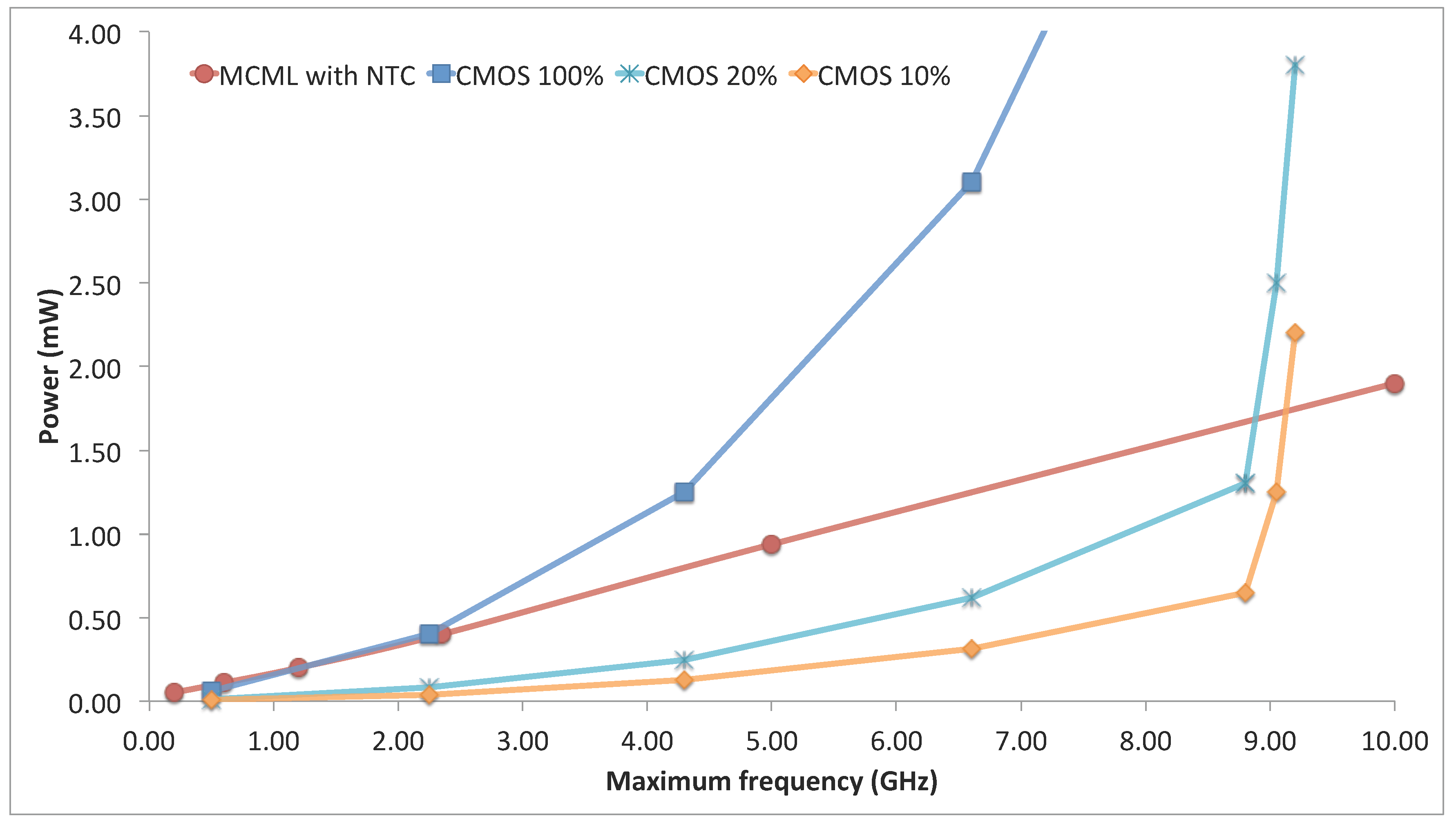
The power, speed, and noise characteristics of standard CMOS and MCML with NTC are presented in the following subsections.

5.1. Power/Speed

The power consumed by a 32-bit Kogge Stone adder is shown in Figure 8, as described in Section 4. As expected from the gate performance characteristics listed in Table 2, MCML with NTC is more power efficient than standard CMOS with NTC when operating at high frequencies.
Three speed/power behaviors of interest are exhibited, as illustrated in Figure 8. At 1 GHz, the power consumed by MCML with NTC is less than standard CMOS at a 100% activity factor. In other words, the combination of MCML with NTC is more power efficient for circuits operating at frequencies above 1 GHz and switching every cycle. These types of circuits are not limited to clock distribution networks.
At around 9 GHz, the CMOS circuit reaches the maximum operating frequency at a nominal supply voltage with minimum sized gates. To further lower the delay (to increase the frequency), the CMOS gates need to be significantly larger. A sharp increase in power consumption is noted for standard CMOS operating at multi-gigahertz frequencies switching at 10% and 20% activity factors. Due to this sharp rise, at around 9 GHz, MCML with NTC is more power efficient than standard CMOS switching at a 20% activity factor.
Figure 8. Power vs. maximum frequency of MCML with near threshold circuits (NTC) and standard CMOS for activity factors of 10%, 20%, and 100%.
Jlpea 04 00138 g008
Additionally, above 9 GHz, MCML with NTC is more power efficient than standard CMOS switching at a 10% activity factor. At these frequencies, MCML with NTC is the methodology of choice for general high performance circuits. Activity factors below 25% represent general switching characteristics of typical data paths.
These characteristics of MCML with NTC position this technology as a significant competitor to standard CMOS when operating at high activity factors, or multi-gigahertz frequencies regardless of the activity factor. Unlike standard CMOS, MCML is capable of power efficient operation at frequencies beyond 9 GHz (in 14 nm technology), enabling power efficient operation at multi-gigahertz frequencies.

5.2. Noise

The maximum induced noise in a power network due to switching activity is listed in Table 3. Noise values are presented for standard CMOS and MCML as a function of power network resistance, capacitance, and inductance. As noted in this table, the SSN in MCML circuits is, on average, an order of magnitude lower than in static CMOS. The low noise environment is particularly beneficial for deeply scaled circuits operating near the threshold voltage that suffer from high sensitivity to process and environment variations.
This capability supports heterogeneous systems that integrate noise sensitive analog circuits with digital logic and memory. In contrast to standard CMOS circuits with significant simultaneous switching noise, extensive effort to isolate sensitive circuits from switching noise is not required in NTC MCML. Additionally, the low noise environment enables lower noise margins, resulting in more power efficient and/or higher speed circuits. This low noise characteristic represents a significant advantage of MCML combined with NTC, particularly in heterogeneous systems [17].
Table 3. Comparison of noise in CMOS and MCML circuits.
Power network parasitic impedancesNoise induced on power network (mV)
Resistance (ohm)Capaitance (fF)Inductance (nH)MCMLCMOSRatio
absolute valueabsolute value
25010.566.2711
25020.949.9211
25040.7014.6421
210011.286.195
210020.959.1410
210041.8113.517
220010.556.2111
220020.939.9611
220040.6612.5619
55011.326.505
55020.849.7512
55041.7114.639
510010.516.5213
510020.939.2910
510040.7213.2418
520011.256.605
520020.8310.0212
520041.6112.168

6. Conclusions

The combination of NTC and MCML exhibits high performance by exploiting the advantages of each technology. The proposed combination of MCML with NTC is shown to be best suitable for two types of applications. The first type are high activity circuits operating at frequencies above 1 GHz (assuming 14 nm FinFET CMOS). This behavior is in contrast to standard CMOS, which dissipates excessive power at high activity factors. The second type are low activity circuits operating at frequencies above 9 GHz. At these high frequencies, CMOS is inefficient due to the linear dependence of dynamic power with frequency. The combination of MCML with NTC, therefore, provides an effective high performance, power efficient circuit technology for high speed and/or high activity applications.

Acknowledgements

This research is supported in part by a grant from Qualcomm. The authors would like to thank Jeff Fischer, Francois Atallah, Kyungseok Kim, and Jihoon Jeong for their technical support and feedback.

Conflicts of Interest

The authors declare no conflict of interest.

References

  1. Salman, E.; Friedman, E.G. High Performance Integrated Circuit Design; McGraw-Hill Publisher: New York, NY, USA, 2012. [Google Scholar]
  2. Kaul, H.; Anders, M.; Hsu, S.; Agarwal, A.; Krishnamurthy, R.; Borkar, S. Near-Threshold Voltage (NTV) Design: Opportunities and Challenges. In Proceedings of the ACM/IEEE Design Automation Conference, San Francisco, CA, USA, 3–7 June 2012; pp. 1149–1154.
  3. Alioto, M.; Palumbo, G. Feature-Power-Aware Design Techniques for Nanometer MOS Current-Mode Logic Gates: A Design Framework. IEEE Circuits Syst. Mag. 2006, 6, 42–61. [Google Scholar] [CrossRef]
  4. Jain, S.; Khare, S.; Yada, S.; Ambili, V.; Salihundam, P.; Ramani, S.; Muthukumar, S.; Srinivasan, M.; Kumar, A.; Gb, S.K.; et al. A 280 mV-to-1.2 V Wide-Operating-Range IA-32 Processor in 32 nm CMOS. In Proceedings of the IEEE Solid-State Circuits Conference, San Francisco, CA, USA, 19–23 February 2012; pp. 66–68.
  5. Dreslinski, R.; Wieckowski, M.; Blaauw, D.; Sylvester, D.; Mudge, T. Near-Threshold Computing: Reclaiming Moore’s Law through Energy Efficient Integrated Circuits. IEEE Proc. 2010, 98, 253–266. [Google Scholar] [CrossRef]
  6. Islam, A.; Akram, M.; Imran, A.; Hasan, M. Energy Efficient and Process Tolerant Full Adder Design in Near Threshold Region Using FinFET. In Proceedings of the International Symposium on Electronic System Design, Bhubaneswar, India, 20–22 December 2010; pp. 56–60.
  7. Hassan, H.; Anis, M.; Elmasry, M. MOS Current Mode Logic: Design, Optimization, and Variability. In Proceedings of the IEEE International SOC Conference, Santa Clara, CA, USA, 12–15 September 2004; pp. 247–250.
  8. Hassan, H.; Anis, M.; Elmasry, M. MOS Current Mode Circuits: Analysis, Design, and Variability. IEEE Trans. Very Large Scale Integr. (VLSI) Syst. 2005, 13, 885–898. [Google Scholar] [CrossRef]
  9. Tang, T.; Friedman, E. Simultaneous Switching Noise in on-Chip CMOS Power Distribution Networks. IEEE Trans. Very Large Scale Integr. (VLSI) Syst. 2002, 10, 487–493. [Google Scholar] [CrossRef]
  10. Abdulkarim, O.M.; Shams, M. A Symmetric MOS Current-Mode Logic Universal Gate for High Speed Applications. In Proceedings of the ACM Great Lakes Symposium on VLSI, Lago Maggiore, Italy, 11–13 March 2007; pp. 212–215.
  11. Mandapati, V.S.R.; Nishanth, P.V.; Paily, R. Study of Transistor Mismatch in Differential Amplifier at 32 nm CMOS Technology. Int. J. Comput. Sci. Issues 2011, 1, 109–115. [Google Scholar]
  12. Kuhn, K. Reducing Variation in Advanced Logic Technologies: Approaches to Process and Design for Manufacturability of Nanoscale CMOS. In Proceedings of the IEEE International Electron Devices Meeting, Washington, DC, USA, 10–12 December 2007; pp. 471–474.
  13. Tawfik, S.; Kursun, V. FinFET Technology Development Guidelines for Higher Performance, Lower Power, and Stronger Resilience to Parameter Variations. In Proceedings of the IEEE International Midwest Symposium on Circuits and Systems, Cancun, Mexico, 2–5 August 2009; pp. 431–434.
  14. Cao, Y.K. Predictive Technology Models. Available online: http://ptm.asu.edu/ (accessed on 29 April 2014).
  15. Kogge, P.M.; Stone, H.S. A Parallel Algorithm for the Efficient Solution of a General Class of Recurrence Equations. IEEE Trans. Comput. 1973, C-22, 786–793. [Google Scholar] [CrossRef]
  16. The International Technology Roadmap for Semiconductors. Available online: http://www.itrs.net/ (accessed on 29 April 2014).
  17. Pavlidis, V.F.; Friedman, E.G. Three-Dimensional Integrated Circuit Design; Morgan Kaufmann: Burlington, MA, USA, 2009. [Google Scholar]

