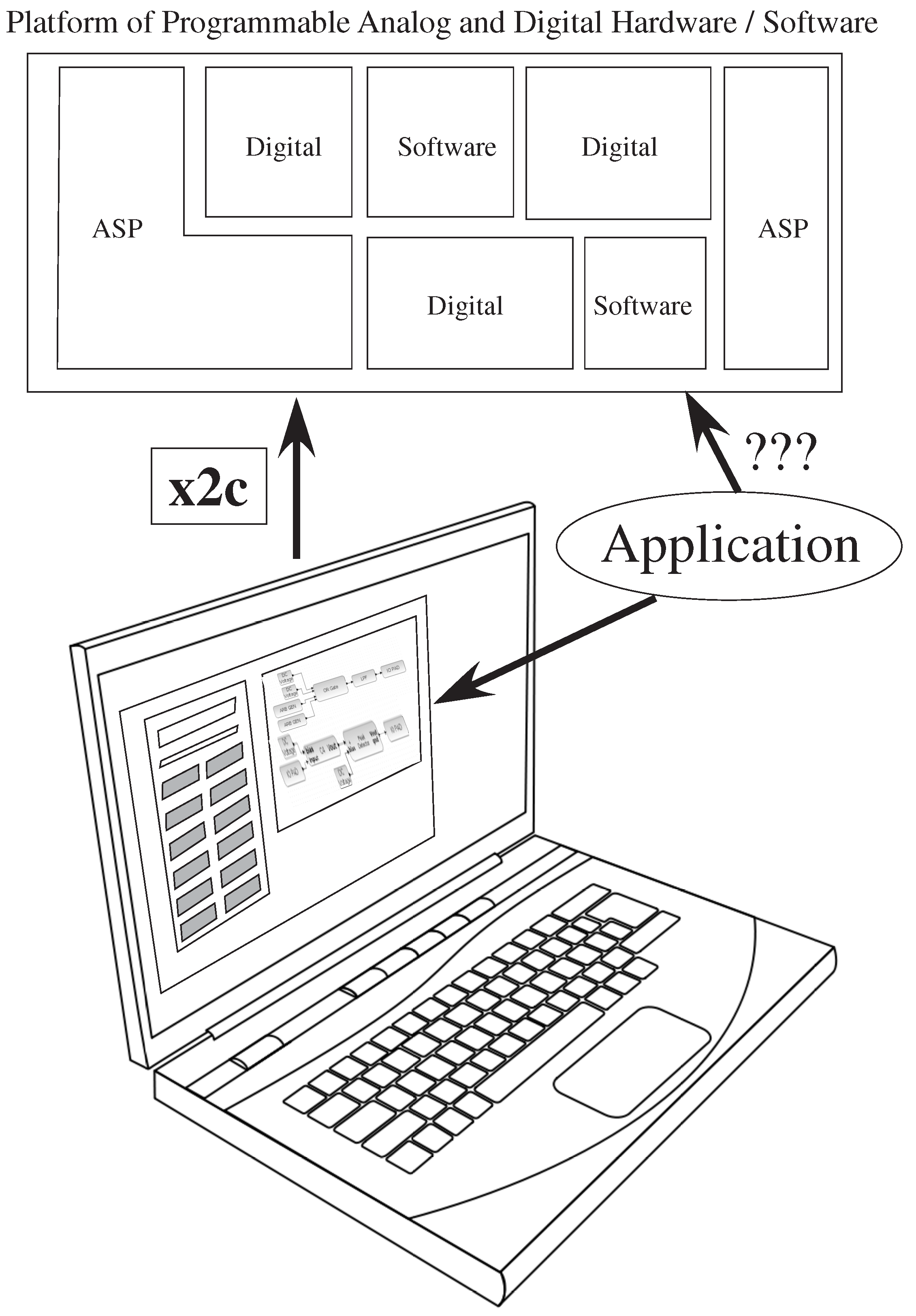
1. Motivation for a Design Tool for Configurable Analog–Digital Platforms
The emergence of large-scale mixed-mode configurable systems, such as the system on chip (SoC) large-scale field programmable analog arrays (FPAA) [
1], shows the need for tools that enable designers to effectively and efficiently design through the large number of open questions in this analog–digital co-design space. This paper presents a unified tool framework for analog–digital hardware-software co-design, enabling the user to manipulate design choices (
i.e., power, area) involving mixed-signal computation and signal processing. This tool set provides a starting point for the analog–digital software co-design discussion to further development through an open-source platform, as larger future mixed-mode configurable systems will be developed.
Digital-only hardware-software co-design is an established, although unsolved and currently researched, discipline (e.g., [
2]); incorporating analog computation and signal processing adds a new dimension to co-design. Well-established Field Programmable Gate Array (FPGA) design tools, such as Simulink [
3], are developed to work with Xlinix [
4] and Altera FPGA [
5,
6] devices. Simulink, and to a lesser extent, some open source tools (e.g., [
7]), provides the framework to input into Xlinix/Altera compilation tools, completely abstracting away the details from the user, by allowing both standard Simulink blocks to compile to Verilog blocks to targetable hardware, as well as support for specific blocks on that hardware platform. Current research in hardware-software co-design focuses entirely on digital hardware-software (e.g., processor) co-design (for example, [
8,
9,
10]).
The wide demonstration of programmable and configurable analog signal processing and computation [
1,
11] opens up an additional range of design choices, but requires user-friendly design tools to enable system design without requiring an understanding of analog circuit components. Occasionally, analog automation tools are discussed [
12,
13]; usually, these treatments are theoretical in nature, because of the lack of available experimental hardware, and not enabling the momentum required to develop working systems, including research lab or classroom demonstrations. This tool set expands the graphical design for analog–digital computational systems in an open-source platform.
The tool integrates a high-level design environment built in Scilab/Xcos (open-source programs similar to MATLAB/Simulink), with a compilation tool,
x2c , Xcos to compiled object code, creating a design environment to instantiate configurable and programmable hardware.
Figure 1 illustrates using the Xcos tool framework compiled down to the system through
x2c, providing a time-efficient method of solution, enabling system designers to integrate useful systems, while still enabling circuit experts to continue to develop creative and reusable designs within the same tool flow. This open-source tool platform integrates existing open-source VPR [
14] with software developed to build an integrated environment to simulate and experimentally test designs on the FPAA SoCs.
Figure 1.
The translation from an application to a heterogeneous set of digital hardware + software resources is a known field of study; The translation from an application to a heterogeneous set of analog and digital hardware + software resources is a question that is barely even considered. The focus of this paper is to describe a set of software tools to encapsulate a range of potential application solutions, written in SciLab/Xcos, that enable a range of system design choices to be investigated by the designer. These tools enable high-level simulation, as well as enable compilation to physical hardware through a tool, x2c. The tool set will be publicly available upon publication of this paper.
Section 2 overviews the analog–digital design tool.
Section 3 describes tool integration with an experimental FPAA platform.
Section 4 describes the methodology for implementing the tool set, including macromodel system simulation corresponding to measurements and translating from the Xcos description to net list descriptions for hardware compilation.
Section 5 describes some larger FPAA system examples.
Section 6 summarizes this paper, as well as discusses strategies for analog–digital co-design. The tool set will be publicly available upon publication of this paper.
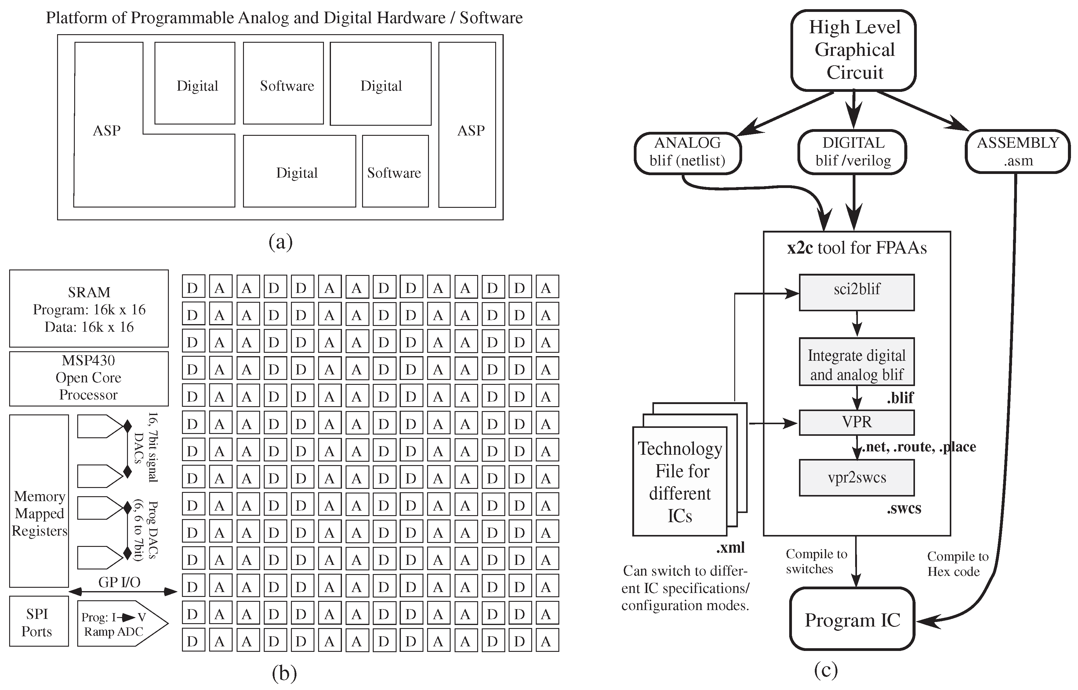
2. Analog–Digital Design Tool Overview
Figure 2 shows the tool set translating from an application to a heterogeneous set of analog and digital hardware + software resources, such as the representative case in
Figure 2a, as well as the specific FPAA integrated circuit. in
Figure 2b.
Figure 2.
Tool design overview to handle programming a mixed platform of programmable analog and digital hardware and software, such as the block in (
a); (
b) a recent large-scale SoC field programmable analog array (FPAA) provides the specific target device [
1]. A particular FPAA system is defined by its different technology files, chosen by the user, encompassing a combination of components with analog (
i.e., computational analog block (CAB)) or digital components (
i.e., computational logic block (CLB)) that are connected through a switch matrix, as well as a range of I/O components and special additional components. (
c) Top-down design tool flow. The graphical high-level tool uses a palette for available blocks that compile down to a combination of digital and analog hardware blocks, as well as software (processor) blocks. The tool
x2c converts Xcos design to switches to program the SoC, combining open-source software like Scilab, Xcos, VPR and custom software
sci2blif and
as a software suite to program and test FPAA SoCs.
![Jlpea 06 00003 g002]()
Figure 2c shows the resulting tool flow block diagram, enabling IC experimental results, as well as system/circuit simulation. The Xcos system is built to enable macro-model simulation of the resulting physical system.
x2c converts an Xcos design to switches to program the hardware system, made up of
sci2blif that converts Xcos to modified
blif (Berkeley Logic Interface Format) and
that converts
blif to a programmable switch list as code around the modified open-source Virtual Place and Route (VPR) tool [
14], a tool originally designed for basic FPGA place and route algorithms. The particular system to be targeted, an FPAA IC, is defined by its resulting technology file for
x2c tool use. A detailed discussion of
place and route tools will be published elsewhere, as it is beyond the scope and length of this paper.
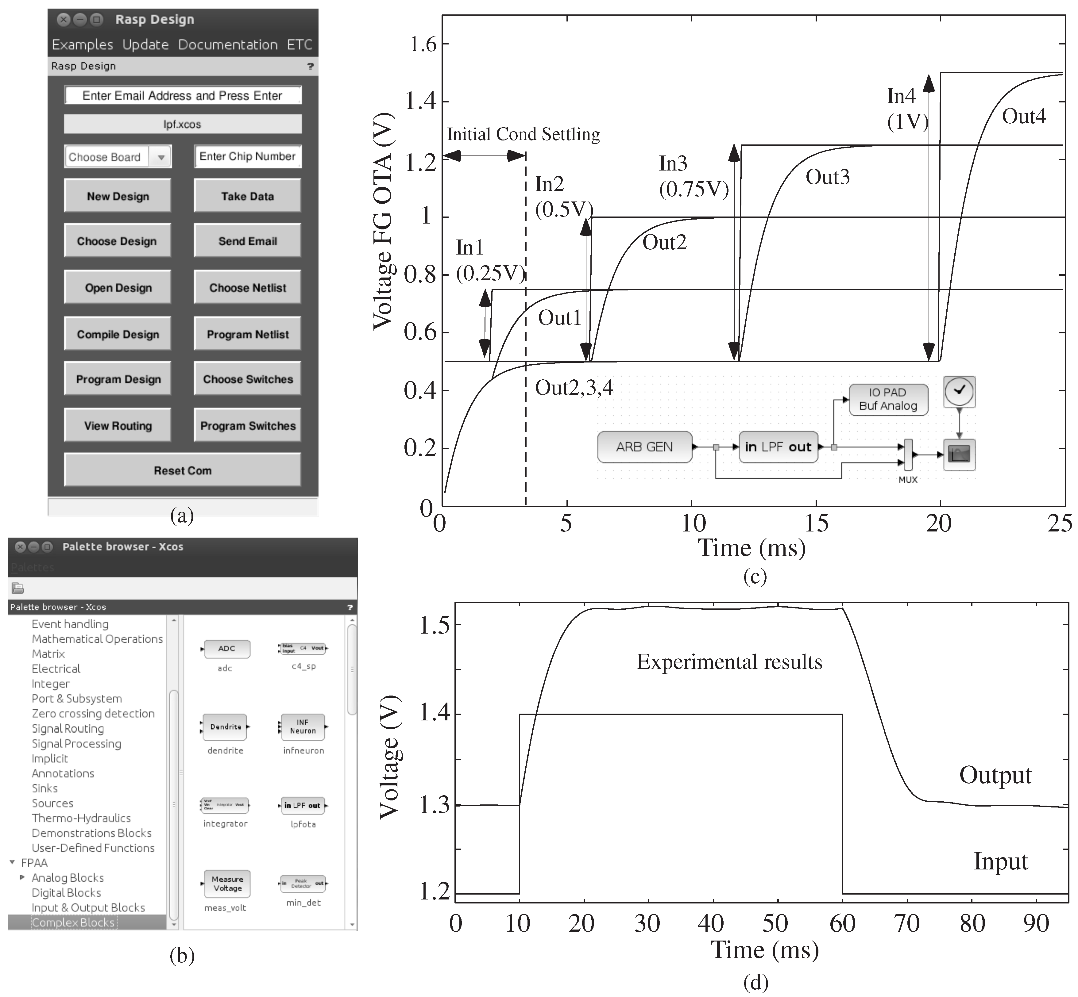
Figure 3 shows a full tool example of the graphical interface and results for a first-order low-pass filter (LPF) system, showing both simulation results and experimental results. The tool is encapsulated in a single, open-source Ubuntu Virtual Machine, with a single desktop button to launch the entire Scilab tool framework. Xcos gives the user the ability to create, model and simulate analog and digital designs. The Xcos editor has standard blocks that are compartmentalized into classes or palettes that range from mathematical operations to digital signal processing. The editor allows the internal simulator to utilize the functionality of each block to compute the final answer. The tool structure took advantage of user-defined blocks and palettes that can interact with Scilab inherent blocks.
Figure 3.
An example of the entire tool flow for a low-pass filter (LPF) computation. (a) The user chooses basic design options through the FPAA Tools GUI, which starts running when the Scilab tools are started in the distributed Ubuntu Virtual Machine (VM); (b) snapshot of the Xcos palette for FPAA blocks. There are four sections, namely the analog, digital, input/output and complex blocks; the analog, digital and I/O blocks consist of basic elements in different tiles of a chip. Complex blocks are pre-defined circuit blocks made of more than one basic element. (c) Simulation results for four input and output computation. Lines, and resulting blocks, allow for vectorized, as well as scalar inputs. Inset shows the Xcos diagram; the user sets parameters for simulation or for compiling into an integrated circuit. (d) Experimental results for a one input and output computation.
The Xcos [
7] tool uses user-defined blocks and libraries. When the user opens the Xcos editor, a palette browser is displayed, as shown in
Figure 3b. The browser lists Scilab’s collection of palettes, as well as user-defined palettes. One selects from a palette of available blocks to build the resulting system, which can be composed of a mixture of analog (
blif), digital (Verilog) and software (assembly language) components. The Palette for FPAA Tools contains sub-palettes for blocks that are classified as analog, digital, inputs/outputs and complex blocks. The input/output palette contains typical circuits, like DACs, arbitrary waveform generator, IO pads and voltage measurement (ADC). The digital palette contains typical circuits, like a digital flip-flop and a clock divider. A few examples of complex blocks are a low-pass filter (LPF), a sigma-delta ADC and a vector matrix multiplier (VMM) connected to a winner-take-all (WTA) block as a classifier structure.
The blocks and their information are stored in a Scilab data structure that can be accessed in two different files, a block interfacing function and a block computational function. The interfacing function sets up the fields of the dialog box associated with each block to retrieve user parameters and set default values, as well as defines the size of the block and the number of inputs and outputs. There are consistency checks to let the user know if the values they entered into the dialog box are a valid implementation.
Each block has two specific files that dictate its appearance and its performance within Xcos. The computational function encourages model customization, while the interfacing function supports built-in data checking, variable inputs/outputs and default parameters. The interfacing and computational functions are heavily coupled by the Scilab structure for a block. Thus, the parameters retrieved from a dialog box displayed to users are accessible to compute the output of blocks during simulation.
This discussion follows a previous representation [
15] of analog blocks into Level 1 and Level 2 blocks. Level 1 blocks abstract away intricacies for system designers, such as the inputs and outputs being vectorized, voltage-mode signals (as seen in
Figure 3c towards the bus of four signals).
Figure 3d shows experimental results for a single line (bus of one signal). Level 2 blocks allow for general circuit design, typically as a representation of computational analog block (CAB) elements. Example CAB elements include Transistors, Floating-Gate (FG) Transistors, Transconductance Amplifiers (TA), and digital transmission gates (Tgate). The TA output current is proportional to the applied voltages for one operating region. Tgate emulates a rail-to-rail switch element in a CMOS process. Each block uses vector signals and resulting vector-based block computation, where each block may represent potentially N virtual blocks (or more) to either be compiled to silicon or simulated. The lines/links that connect the blocks together are essentially layered buses. Each link, and resulting block element, allows for vectorized signals, as seen by the example in
Figure 3c (four signals on one line for simulation), consistent with the Level 1 definition [
15], empowering the user to develop systems with just the necessary number of blocks.
3. Integrating the Analog–Digital Design Tool with an FPAA Platform
The test platform is a full system IC requiring only simple interfacing to the outside world through USB ports, appearing to be a standard peripheral to a typical device.
Figure 2b shows the block diagram of the SoC FPAA used in this paper for experimental measurements. This SoC FPAA enables nonvolatile digital and analog programmability through floating-gate (FG) devices, both in the routing fabric, as well as in CAB block parameters (
i.e., bias current for an OTA). The blocks with simply digital (D) components are called computational logic blocks (CLB), and the blocks with analog (A) and digital components are called computational analog blocks (CAB). Further, the use of FG devices for switches effectively embeds analog components into the routing fabric, as well as enabling connections on the resulting lines [
16], often allowing far more computation in just the routing fabric compared to the CAB or CLB elements. Any tool development for these FPAA SoC must be able to handle these opportunities; almost all configurable systems have some similar opportunities that must be encoded in the system’s technology file. Other FPAA devices fit into this general framework [
17,
18,
19,
20,
21,
22].
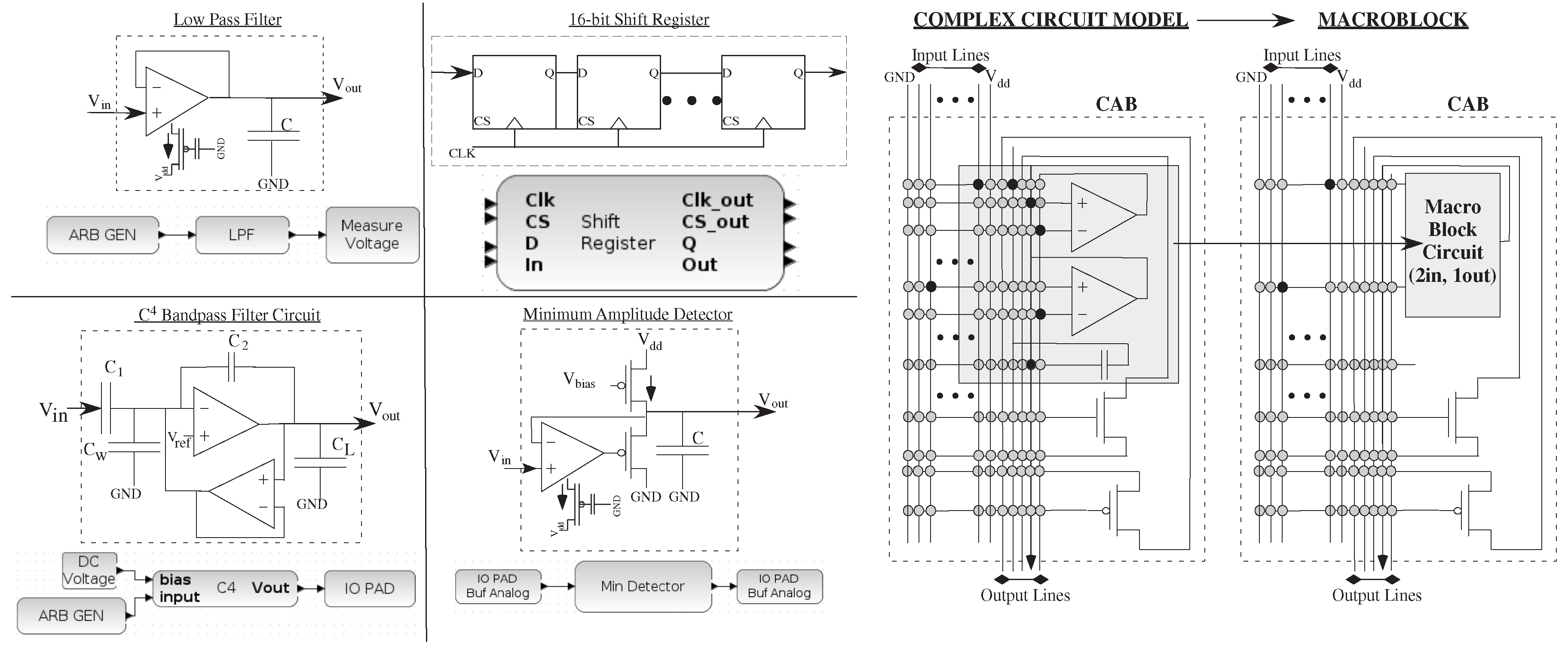
Figure 4 shows descriptions of component blocks in the library (all level = 1 block) and their resulting circuit schematics, including filters, counters and detectors. Although a circuit expert gains tremendous insight into the particular circuit being compiled and used on the IC, most system designers are satisfied with getting the desired functional behavior, with minimal non-idealities from the circuit. The result is a rich set of analog and digital blocks, similar to FPGAs when using graphical design tools (
i.e., [
3]), that can be expanded and grown as needed. The DC voltage block in
Figure 7 and
Figure 8 is an FG programmed transconductance amplifier to provide a programmed, low-impedance DC voltage output directly from the voltage set in Scilab.
Figure 4.
An example of a range of low-level circuit components and their block diagram, as well as some of their testing circuits, which include analog and digital components. We show a LPF (as seen in the previous example), a minimum amplitude detector, a capacitively coupled current conveyer (C) band-pass filter, and a digital shift-register block. The result allows us to draw in block diagrams for mixed-mode computation; in each of these cases, the inputs could be a scalar or a vector; In each case, one often wants to encapsulate the knowledge of the designer as much as possible in the resulting design. For example, the original analog designer might want a group of circuits all in a single CAB; a macroblock encapsulates a single block in a CAB that is built from basic elements in the analog and digital tiles, using separate black boxes in VPR to keep all elements in the same tile.
Figure 4 also shows typical CAB components and typical routing infrastructure of input and output port lines to the rest of the Manhattan geometry routing fabric, including the detailed routing to compile the C
bandpass filter circuit. A macroblock encapsulates complex circuits using elements inside a single tile to create a single block, enabling more efficient high-level routing where the connections within the CAB are pre-optimized, requiring the tool only to handle placement and global routing. Macroblocking encapsulates much of the objectives of the circuit designer, often started at a Level 2 block, as it becomes a full level = 1 block.
4. Methodology for Implementing the Tool Set
This section dives deeper into the key aspects of the high-level tool infrastructure.
Figure 3 shows the same Xcos block diagram structure used for both macromodel simulating and compiling to hardware. This section follows the level = 1 definition [
15], as defined elsewhere and first fully implemented in this work.
For level = 2 cases, the compilation to blif/Verilog from Xcos follows the same path as level = 1, but the simulation environment requires a far more complex simulation environment. Simulation in level = 2 requires compiling the net list into a SPICE model, direct measurement after compilation or developing a simulation framework using Modelica with Scilab; this last topic will be the topic of future discussions.
The following sections address, in turn, the aspects required for level = 1 macromodeled simulation, led simulation and, then, the aspects required for sci2blif, which converts the Scilab structure into a format ready for place and route compilation.
4.1. Macromodel Simulation
A typical design flow includes simulating a design’s functionally, analyzing the results and iterating to a good solution before proceeding to hardware synthesis, often because of the constraints of accessing such a hardware system. At first, one might ask if physical hardware is directly available (and portable), why not always go directly to circuit measurement, getting precise results in real time. Even in cases where hardware is available, it is often useful to have one simulation case, say for DC values and a reference simulation, to compare with experimental measurements. The amount of simulation one might do before compiling a circuit will depend on compile time (longer compile time, more simulation), accessibility to FPAA hardware, whether in person or remote, user inexperience (more inexperienced, longer simulation time), as well as the number of potential debugging points required.
The simulation focuses on an as fast as possible simulation model that gives accurate results, unlike generalized SPICE models require, including every possible transistor configuration and situation. A given macromodel has precisely one specific case related to a particular hardware device, greatly simplifying the resulting computations. The resulting simulation results and experimental results should be reasonably close (i.e., within 1%–5%), while at just enough computational complexity. Scilab, like MATLAB, optimizes for vector operations; vectorization of blocks preserves this functionality, as well as results in the fastest numerical simulation possible.
The analog system modeling requires using ordinary differential equations (ODE), potentially in combination with algebraic equations, that capture the continuous-time circuit nonlinearities. Scilab also enables discrete time modeling, as well as modeling for clocked systems in a similar manner. In the SoC FPAA, every connection point will have some capacitance, resulting in dynamics where the resulting capacitor voltages would often be the state variables. The required form for Xcos/Scilab for ODE simulation is the standard form of:
where
is the vector of state variables (
i.e., voltages) and
is the vector of system inputs. The resulting ODE definition is put into the computation function code using this functional form.
Figure 5 shows an example to formulate a physically realistic model for a C
BandPass Filter (BPF). A particular system will require reformatting these vectors from typical circuit analysis. Then, the example C
bandpass filter is modeled at the circuit function, not just the linear transfer function shown elsewhere. Nonlinearities are modeled accurately (as seen by the
function) to enable a system designer to minimize the effect where needed, as well as to empower a designer to utilize nonlinearities when desired.
Figure 5 shows three mathematical iterations required to transform typically written circuit equations into their proper Xcos simulation form, as well as Xcos simulation data from this model; the simulation data corresponds closely to the experimental data.
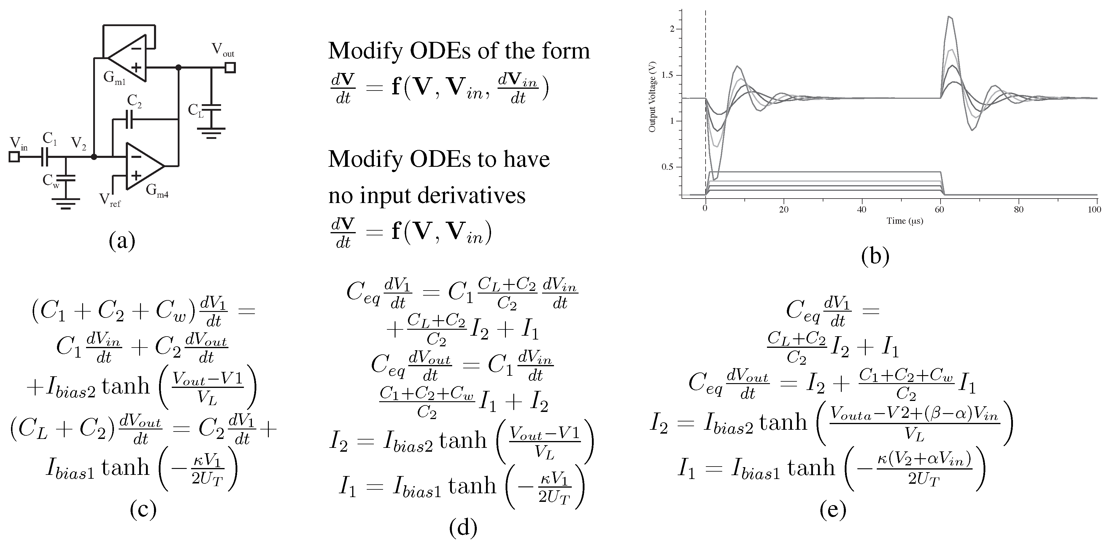
Figure 5.
Approach to building a level = 1 macromodel for the C filter that corresponds closely to measured experimental data. (a) Circuit diagram for a C bandpass filter; (b) simulation of a step response for the C bandpass filter; (c) starting equations from the circuit in (a); (d) modification of the equations into the 1st form; (e) modification of the equations into the final Xcos ODE formulation.
4.2. sci2blif: Xcos → VPR
When the user presses Compile Design on the graphical interface, Scilab calls up sci2blif, which uses the Xcos representation to create a circuit format in blif/Verilog for the place and route tools to create a switch list, as well as gathers the resulting assembly language modules. Analog blocks are converted through sci2blif into a blif format. Digital blocks use VTR to convert from Verilog into a blif format. The switch list represents the low-level hardware description (i.e., switches to be programmed).
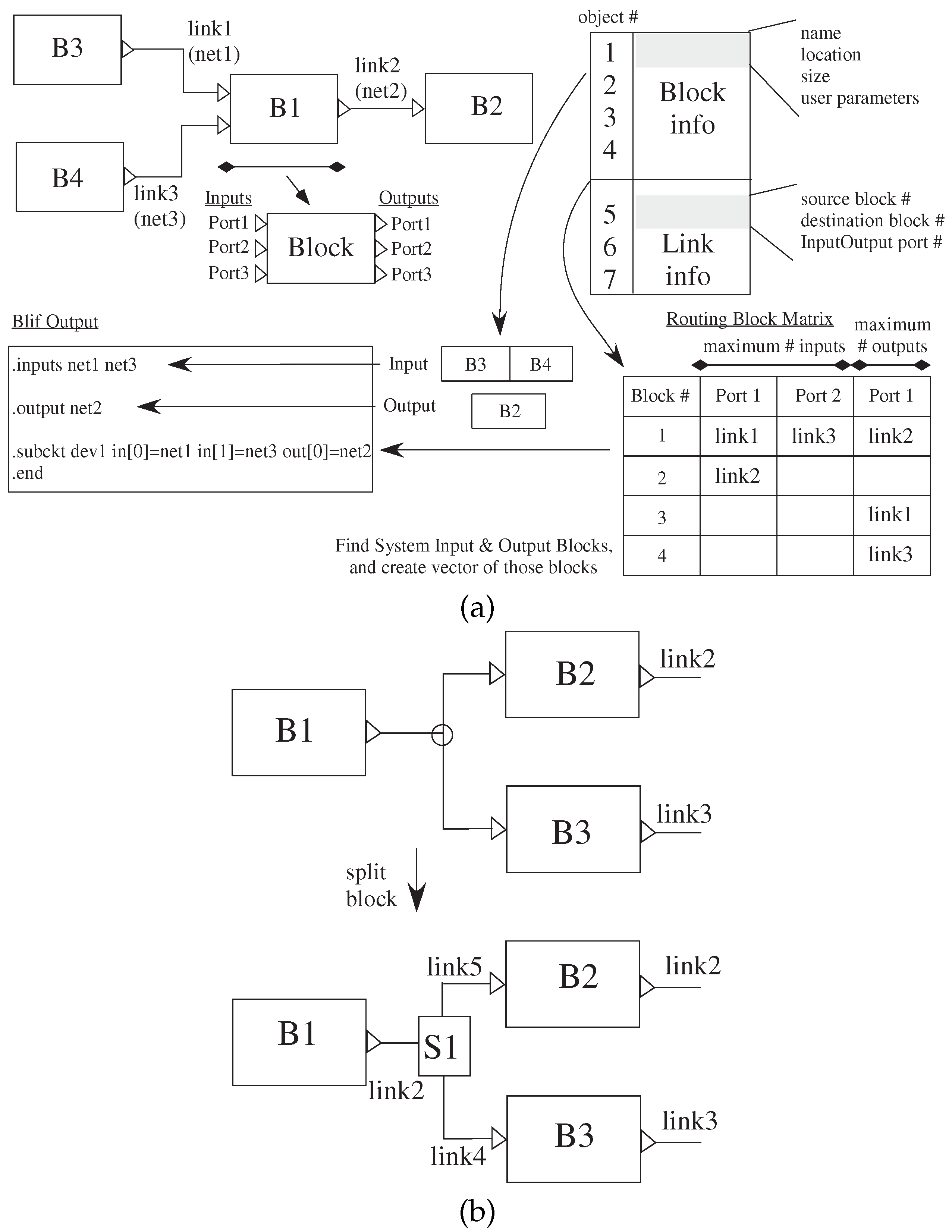
Figure 6 illustrates converting from Xcos visual representation to
blif files for the analog components; the digital procedures are similar, although typically simpler. Scilab saves the graph as a data structure, shown in
Figure 6a, that describes the Xcos file contents. The block objects are listed first, followed by the link objects, and then, they are listed by link numbers.
The high-level Xcos file is converted into three passes over the data structure. The first pass parses over the blocks portion to determine the number of blocks that are compiled to CAB/CLB, input blocks and output blocks. The input and output block object numbers are saved in two separate vectors (a and b, respectively). B is the number of blocks; I is the number of inputs; and O as the number of outputs. Finally, the object is represented as a matrix, G, of size [(B + I + O) × B], that contains the net numbers corresponding to each of the blocks to be compiled.
The second pass parses
to determine which block’s input or output port is connected to another block’s input or output port. Each link is represented by two values: the source and destination in
. The information provided is the block number, port number (ports on blocks are numbered top-down for inputs and outputs) and if the port is an input or output. The net number is placed in the matrix mentioned above. The third pass parses
to generate resulting
blif statements for compilation. The input and output vectors and the matrix are used to put the nets of inputs and outputs at the beginning of the
blif file. Then, for each case, the command for each block is identified, where the net numbers are retrieved from the matrix using the block number.
Figure 6c shows when users connect an output of a block to at least two inputs, an extra small block is inserted into the Xcos internal representation, increasing the number of blocks and links that is removed before generating
blif file.
Figure 6.
sci2bliff fundamentals: Xcos model to blif/Verilog net list to put into VPR. (a) The data structure for a single set of blocks is an array with the block information, as well as link information. Blocks are enumerated by when they are created in Xcos; links are enumerated by where they are located on the block. This data structure transforms to blif representation for VPR. (b) The resulting data structure of the Xcos network only allows for a single input and output for a particular link; therefore requiring additional blocks included to handle when converting a single output going to multiple inputs.
4.3. Integrating the μP Toolflow
This FPAA IC presents the opportunity of integrating
μP code with the configurable analog and digital fabric, creating the challenge of design partitioning, as well as integrating assembly code blocks into the macromodeling simulation and implemented system. For example, the arbitrary waveform generation block in
Figure 3,
Figure 7 and
Figure 8 is an example of a block with high assembly language code content. The voltage output goes through one of multiple signal DACs on the resulting IC. From the vector defined in Scilab, the processor memory space is allocated for this operation; assembly code is generated and integrated into the resulting FPAA programming flow. A similar block is used for recording data through one of multiple ADCs that are available either directly on-chip or compiled on-chip.
One builds assembly blocks similar to analog or digital FPAA fabric blocks. The designer would write and test the resulting assembly code block and abstract its function. The resulting digital blocks are Level 1, with macromodel simulation as Scilab code written by the block designer. These simulations typically utilize the discrete-time simulation modeling available.
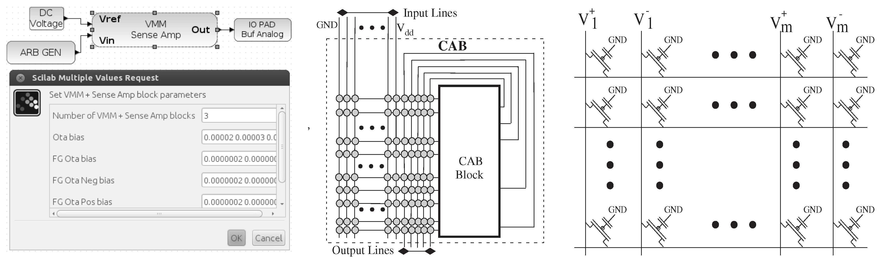
Figure 7.
A key feature to these tools is the ability to build useful computation out of routing resources; for example, the synthesis, place and routing of circuits containing vector-matrix multiplication (VMM) built out of routing (i.e., floating-gate) switches. From left to right, block diagram and parameters for a VMM block, VMM built from a crossbar switch matrix and local interconnect routing resources inside an analog tile.
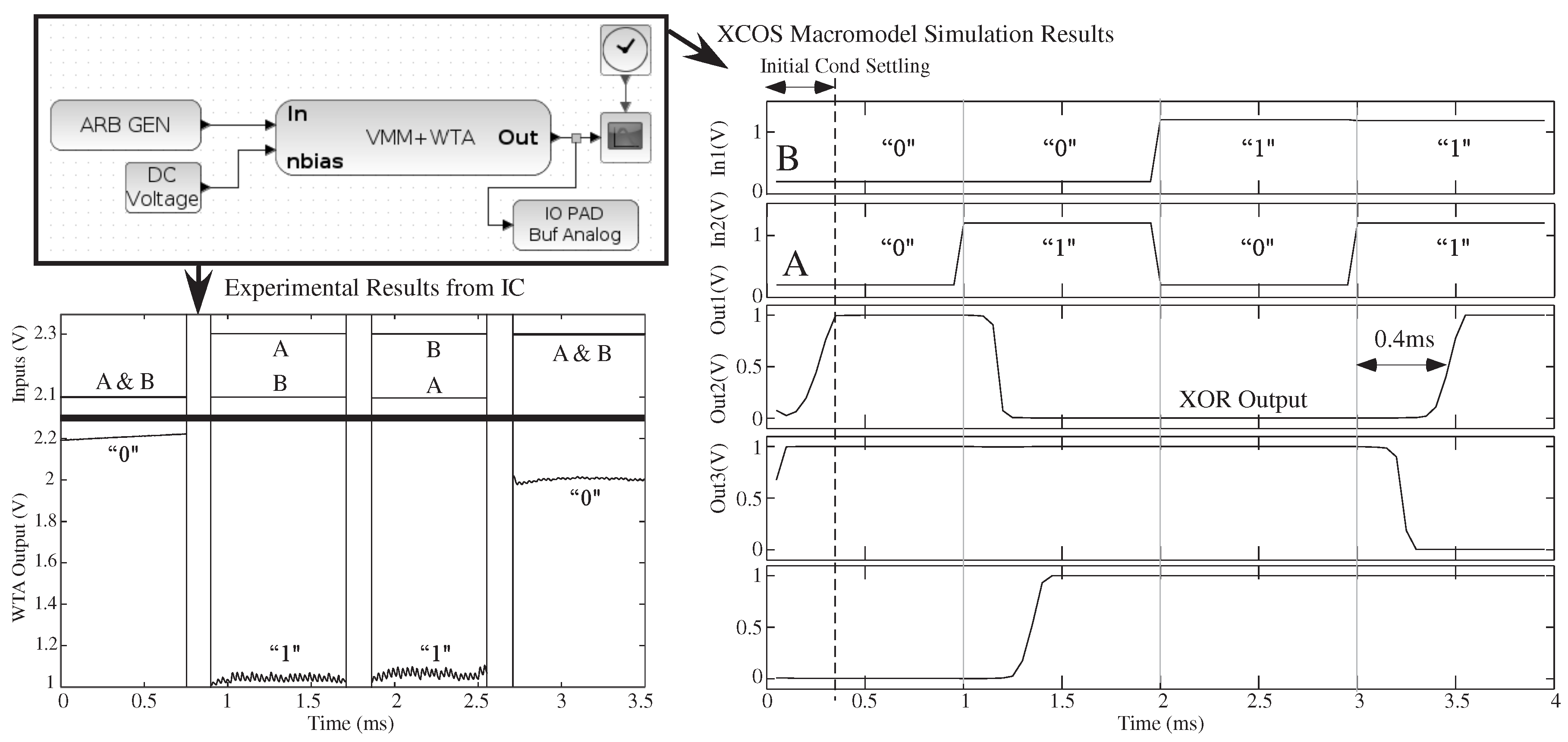
Figure 8.
A system example showing a basic circuit classifier built from a three-input × three-output VMM + winner-take-all (WTA) to represent a classifier function. The Xcos circuit diagram, with its vectorized connections, can be simulated through Xcos Macromodel simulation, as well as compiled and measured experimentally on an FPAA IC. The three input vectorized system, with a 3 × 3 VMM, is configured as a two-input XOR gate (one input fixed). The functional and dynamic behavior agrees well; although the signals have different DC offsets.
The challenge in general in developing a general set of digital blocks is developing a nano-size operating system (100–300 bytes) on the processor. Minimizing the reliance on large on-chip memory size is critical, as the microprocessor is eight times smaller than 16 k (16-bit word) memory (measured and designed across processes from 350 nm–40 nm). One sees that large memory space is highly expensive and power hungry for embedded applications. This design tool interface provides developer-friendly system design without requiring a large embedded system memory; the primary reason for larger operating systems is for the ease of developer design. The resulting tool also requires being able to estimate the resulting memory required for all blocks and making that information available to the user.
5. Simulation and Experimental Data from the Compilation Tool Example
This section shows the compilation of a system example, particularly using the routing components as computational elements. The work in [
1] shows a number of further examples compiled using this FPAA tool set; these two examples illustrate the resulting tool set approach, not to show the capability of the particular FPAA device. Currently, we have tested the particular SoC device to operate on a 1-MHz frequency and where macromodeling simulation, unsurprisingly, reaches similar levels without any further issues.
A crossbar array of these analog programmed FG switches could compute an analog vector-matrix multiplication (VMM), common in all signal processing operations, entirely in routing fabric. The inclusion of such capabilities requires additional sophistication at all levels of the tool flow.
Figure 7 shows an Xcos vectorized block diagram to implement a VMM structure, as well as its implementation using a local routing crossbar array, as well as circuit representation, for a VMM computation. The SoC FPAA [
1] uses FG switches to enable analog computing devices when programming a switch to an analog value. This circuit requires a current-to-voltage conversion, in this case a transimpedance amplifier of two OTA devices, to be consistent with level = 1 requirements. The resulting block has a dialogue box for key parameters.
The VMM + winner-take-all (WTA) classifier both elegantly compiles into FPAA devices using the VMM through FG routing fabric, but further, the classifier combination using a k-WTA is a universal approximator in a single classifier layer [
23].
Figure 8 shows a VMM + WTA circuit used as a classifier circuit, where the VMM block is a single, vectorized block.
Figure 8 shows VMM + WTA macromodeled simulation data and led simulation data. The vectorized block models this circuit as three (vectorized) key equations. These macromodel equations start from starting sub-threshold transistor equations with realistic approximations, such as some transistors in saturation, where experimentally verified. The VMM computation, based on FG devices, with outputs into the cascaded WTA inputs, is modeled:
The transistor operation, modeling the high-gain and negative feedback aspects of the WTA block, computes with the representation:
where
are the input gate voltages (around a steady-state bias voltage) for a classic WTA circuit [
24] and
is the common-source voltage (around a steady-state bias voltage) for the extended differential pair structure for a classic WTA structure [
24], resulting in the following (algebraic) modeling equations:
where the vector of ones (
) and
is a constant relating a coefficient related to biasing values around their steady-state point. The output termination uses typical common-source/common-gate amplifier configuration based on the value for
A and
Z.
Figure 8 shows experimentally-measured VMM + WTA data from the same vectorized test system. The vectorized input, vectorized output VMM + WTA block represents a single block with the size of the classifier determined by the user. A two-input classifier (one input fixed) with a 3 × 3 VMM matrix demonstrates XOR functionality; for WTA circuits, a low output voltage signifies a winner.
6. Summary and Approaches for Analog–Digital Co-Design
This paper presented an analog–digital software-hardware co-design environment and focused examples as mixed-signal design using FPAA SoCs. The tool simulates designs, as well as enables experimental measurements after compiling to SoCs in the same integrated design tool framework. The tool set is an open source setup as an Ubuntu virtual machine enabling straight-forward user setup, as well as open to contributions from third party users empowering a wider community to do analog and digital system design. Digital co-design questions pose issues for systems of mixed hardware (i.e., FPGA) and software (i.e., code running on processor(s)) on the particular partitioning of the resulting computational system based on metrics of power, area, time to market, etc. The recent including of programmable and configurable analog computation allows this community to revisit fundamentally these tradeoffs and issues, already a vibrant field.
The need for large-scale design tools for SoC FPAA devices was the practical driver to create our tool set, although the approach is entirely extendable to a wide range of analog–digital programmable-configurable systems.
x2c in Scilab converts high-level block description by the user to blif format, the input to the modified VPR tool [
14], utilizing
(scilab →
blif), as well as modified architecture file. The resulting tool builds an analog, as well as mixed-signal library of components, enabling users and future researchers to have access to the basic analog operations/computations that are possible.
The designer has a few tools available to handle analog–digital computation that are capable of block level simulation, particularly of a fast high level simulation tied to experimental data, as well as compile to experimental hardware, such as the SoC FPAA IC example used in this writing. Digital FPGA devices have tools that work with Simulink (MATLAB) [
3,
4,
5,
6], and this work provides the first step along the journey to enable similar tools for analog–digital computing systems. The alternative approach requires analog and mixed signal design expertise, often multiple people, for a bottom-up design of a particular custom system using Cadence, Mentor Graphics or similar tools with their associated costs and complexity [
25,
26], or starting with a tool to configure single IC of pre-built fixed components (“proven resources”) interconnected by an optional metal layer [
27].
Having devices of the complexity of the SoC FPAA IC make such tools essential, not just nice to have, for system design. As the call for open FPGA architectures and tools grows stronger (e.g., [
28]), this effort includes and, through including analog computation, expands on this original vision. Simply writing simulation code in MATLAB might find a way forward on simulation, but not on compiling the actual design, or having confidence that the compiled design will work. System design is rarely constrained by good high-level algorithm ideas, but rather resources that connect the high-level algorithm ideas all the way through hardware; this tool set enables such a direct design, encoding the wisdom of the hardware designers where possible in the block library.
How one handles component variability is important when typically dealing with analog (or mixed-mode) systems. For the SoC FPAA, the FG programming allows for directly accounting for, and solving of, the dominant source of errors, MOS transistor threshold voltage (V) mismatch. The variability of devices would be a natural extension of these tools (although not solved at the time of writing this paper), particularly using the hardware compilation to predict the parasitic components accurately by knowledge of a particular device location and routing details, using this information for precise current measurement. Specific known mismatches can be tabled to be used when programming a particular component; the user could create one or multiple random cases if a particular targeted device is unknown.
This open-source tool set explicitly enables a wider user community for mixed-signal configurable designs. A single Ubuntu 12.04 Virtual Machine (VM) encapsulates the entire tool flow, from Scilab/Xcos, device library files, through
sci2blif,
vpr2swcs and modified VPR tools, simply requiring pressing one button to bring up the entire graphical working tool set. Openly distributing this tool set as an open-source virtual machine ( available at
http://users.ece.gatech.edu/phasler/FPAAtool/index.html) for classroom use, research groups, as well as interested users encourages a user community around these tools, as well further improving the tool set. The move to this open source Scilab/Xcos environment from the earlier proto-tools developed in Simulink [
15] enables easy integration with the UNIX-based modified VPR tool, including modifications to enable Manhattan geometries and on-chip microprocessor, as well as fully implement the proposed level = 1,2 concepts previously described. Further, the research group is working to make some FPAA devices, like the SoC FPAA device, available to the larger community, as well as developing systems to enable remote use of existing FPAA devices.
At this point, how comprehensive are the current and envisioned library of tool components is not entirely known. The field of analog computation is still working on understanding its fundamental blocks, a process enabled by building this tool and the resulting user components. The current size of the analog and digital library is relatively small, generated by a handful of people currently, but expected to continue to expand, as the core tool framework is integrated into collaborative research projects, classroom exercises and others using this open-source framework. The blocks currently are composed of the representative VMM block, VMM + WTA (classifier) block, filter bank (particularly BPF , but also LPF), amplitude detect blocks, programmable arbitrary waveform blocks, shift registers, counters, multiple digital logic blocks, DAC block and ADC block, that include analog + digital + μP components, such as ramp and sigma-delta approaches, as well as processor blocks for data handling and ADC control that include compiled signals to interrupts. We expect future publications will report a number of new spatio-temporal processing blocks and will make their resulting blocks also openly available.
A remaining question is understanding the conceptual framework to guide the designer in these analog–digital co-design problems; the following discussion summarizes some of these issues. Current implementations perform all computation in programmable digital hardware, and typically, one wants to minimize the amount of analog processing.
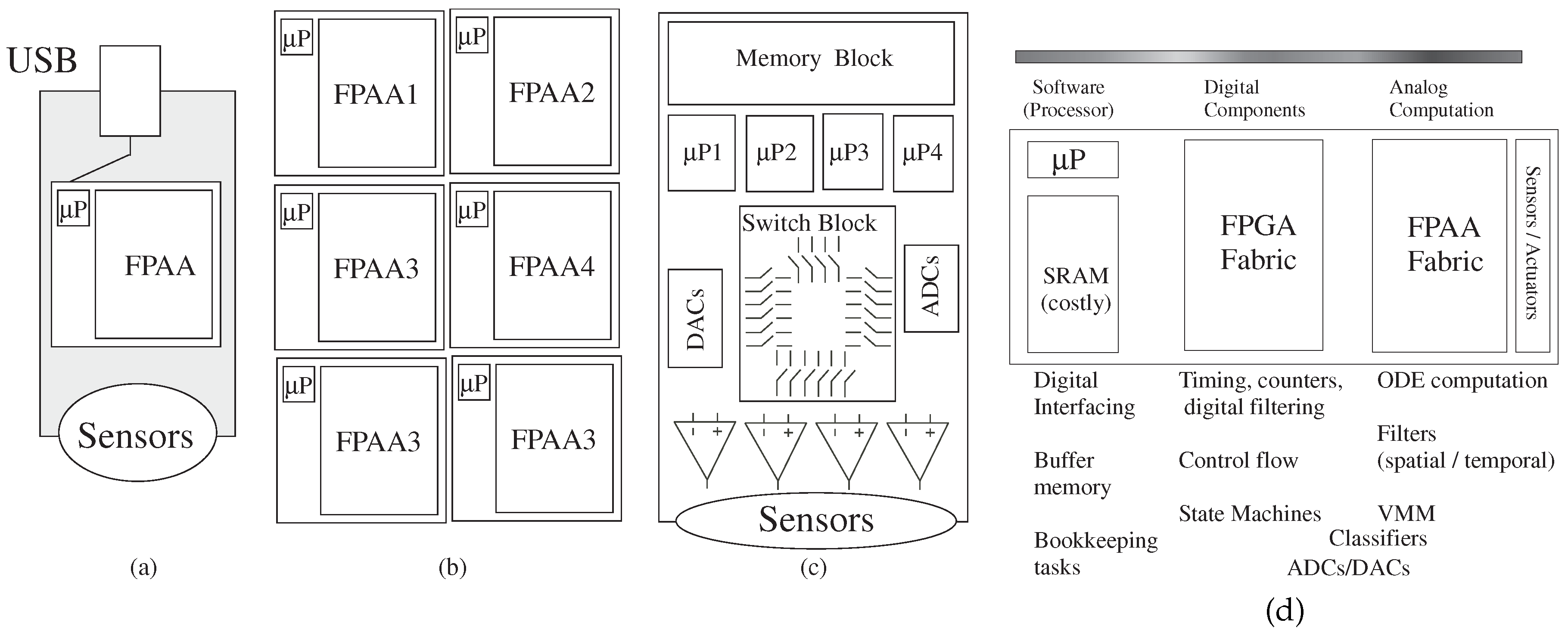
Figure 9 shows designs with a single FPAA IC, with multiple ICs, with a rack of boards, as well as with a set of other components that have some programmability. The high-level graphical tools enables a user to be able to try different algorithms to optimize the system performance, allowing consideration of tradeoffs of power, system utilization, time to market,
etc.
Figure 9.
Possible implementation targets for mixed-mode computing systems. Implementation could be a (a) single FPAA device, (b) a board of FPAA devices or even (c) a board with no FPAA devices, but with programmable parameters and topology for a resulting board encoded in the resulting technology file; (d) a heuristical guide in the analog–digital hardware–software system co-design for such computing systems.
Figure 9d illustrates initial starting guidelines for the problem partition. In particular, one will typically want the heavy computation as physical computation blocks near the sensor where the data originates or transmits; ideally data flow architectures minimize the amount of short-term storage elements (power and area issues). Moving heavy processing to analog computation tends to have less impact on signal line and substrate coupling to neighboring elements compared to digital systems, an issue often affecting the integration of analog components with mostly digital computing systems. Often the line between digital and analog computation is blurred, for example for data converters or their more general concepts, analog classifier blocks that typically have digital outputs. The digital processor will be invaluable for bookkeeping functions, including interfacing, memory buffering and related computations, as well as serial computations that are just better understood at the time of a particular design.
The algorithm tradeoff between analog and digital computation directly leads to the tradeoff between high-precision with poor numerics of digital computation versus the good numerics with lower precision of analog computation. Digital computation focuses on problems with a limited number of iterations that can embody high precision (e.g., 64-bit double precision), like LU decomposition (and matrix inversion). Classical digital numerical analysis courses begin with LU decomposition and move to significantly harder computations in optimization, ODE solutions and PDE solutions; many engineering problems try to move computation towards matrix inversion and away from ODE solutions.
Analog computation focuses on problems tolerant of lower starting precision for computation, such as ODEs and PDEs. Simple operations, like VMM, are fairly similar in tradeoffs between analog and digital approaches, particularly when using real-world sensor data starting off with lower precision (e.g., acoustic microphones at 60 dB, CMOS imaging at 50–60 dB, etc.). Many ODE and PDE systems have many correlates in other physical systems found in nature that are the focus of high performance computing. The resulting time/area efficiencies for analog computation, directly being a model physical system, are valuable for low-latency signal processing and control loops. One would want to avoid analog LU decomposition where possible, while one wants to avoid solving a large number of ODEs and/or a couple PDEs by digital methods. Developing a parallel discipline for analog numerical analysis remains an open question, although potentially reachable question in the near term.


