Review

Low Power Design for Future Wearable and Implantable Devices

Department of Engineering, Aarhus University, Aarhus 8000, Denmark
*
Author to whom correspondence should be addressed.
J. Low Power Electron. Appl. 2016, 6(4), 20; https://0-doi-org.brum.beds.ac.uk/10.3390/jlpea6040020
Submission received: 25 July 2016 / Revised: 27 September 2016 / Accepted: 12 October 2016 / Published: 20 October 2016
(This article belongs to the Special Issue Recent Advances in Emerging Low Power Circuits and Systems)

Abstract

:
With the fast progress in miniaturization of sensors and advances in micromachinery systems, a gate has been opened to the researchers to develop extremely small wearable/implantable microsystems for different applications. However, these devices are reaching not to a physical limit but a power limit, which is a critical limit for further miniaturization to develop smaller and smarter wearable/implantable devices (WIDs), especially for multi-task continuous computing purposes. Developing smaller and smarter devices with more functionality requires larger batteries, which are currently the main power provider for such devices. However, batteries have a fixed energy density, limited lifetime and chemical side effect plus the fact that the total size of the WID is dominated by the battery size. These issues make the design very challenging or even impossible. A promising solution is to design batteryless WIDs scavenging energy from human or environment including but not limited to temperature variations through thermoelectric generator (TEG) devices, body movement through Piezoelectric devices, solar energy through miniature solar cells, radio-frequency (RF) harvesting through antenna etc. However, the energy provided by each of these harvesting mechanisms is very limited and thus cannot be used for complex tasks. Therefore, a more comprehensive solution is the use of different harvesting mechanisms on a single platform providing enough energy for more complex tasks without the need of batteries. In addition to this, complex tasks can be done by designing Integrated Circuits (ICs), as the main core and the most power consuming component of any WID, in an extremely low power mode by lowering the supply voltage utilizing low-voltage design techniques. Having the ICs operational at very low voltages, will enable designing battery-less WIDs for complex tasks, which will be discussed in details throughout this paper. In this paper, a path towards battery-less computing is drawn by looking at device circuit co-design for future system-on-chips (SoCs).

1. Introduction

One of today’s major challenges in circuit design is lowering the power consumption of electronic circuits. The increasing demand for higher computation power has led to the development of sub-micron and nano scale transistors in order to enable a higher density of components in a chip. However, because of the decreasing size, problems such as Short Channel Effects (SCE) and process variations are limiting the reliability of the circuits. In addition, the rising current density in the silicon challenges manufacturers because of the excess heat generated by the power dissipation, which will decrease the reliability and life span of the circuits. This problem is becoming increasingly severe in the nano-range transistors because, not only does the power density increase when more transistors are fit into smaller regions, but the leakage power of the transistors is also becoming comparable to the dynamic power consumption, which means that a great deal of the power spent, is wasted solely on heat generation [1]. This can be dealt with by further researching cooling and packaging in order to avoid overheating the circuits; however, this is an expensive and time limited solution, so this paper addresses methods to generally reduce the overall power consumption of the systems.
Since the Internet of Things (IoT) revolution, a new focus has been made on making smart phones, smart watches, tablets etc. even smaller whilst increasing the computation power. And with the recent interest in the Internet of Bio-Nano Things (IoBNT) [2], the focus has moved from just increasing the computation power to also creating extremely compact, ultra low power designs that enable small sensors and actuators to operate independently of wired data connections and external power sources. Especially for implanted sensors, the size restriction is crucial for the bio-compatibility and therefore, it is rarely an option to attach bulk batteries to the implant. Instead they will be powered by scavenging the surroundings for ambient energy. This focus is particularly interesting in the medical field, where a lot of research is dealing with implants and other wearable devices that monitors physical responses from the body. Also sporting equipment has a huge market already, in producing different bio sensors that monitors the physical state of athletes.
This development calls for new technologies on several fronts, both on device level and circuitry, systems and applications. To continue and develop more energy efficient systems, device circuit co-design techniques are necessary. As mentioned before, downscaling of component footprint can bring about more compact designs, however to address the rising challenges, new devices such as Multi-Gate Field-Effect Transistors (MuGFETs), Carbon Nanotube FET (CNT-FET), Spin-based FET (Spin-FET) etc. have been proposed.
In this article, we will highlight the FinFET device as the most promising alternative and explain the recent strategies to obtain more efficient circuitry in the low power regime, both in digital and analog domain. Furthermore, we will describe techniques to lower the power consumption of a design including digital, analog and memory blocks. In the end, popular energy harvesting methods will be introduced and the possibilities for powering entire low power systems using energy harvesting, will be discussed. The remainder of the paper is organized as follows. Section 2 and Section 3 describes the design techniques and challenges in digital and analog domain including a discussion on CMOS and FinFET device characteristics and some basic blocks including memory and amplifiers. In Section 4, the existing energy harvesting techniques for a self-powered battery-less WID is explained in details. In Section 5, the conclusion is drawn.

2. Low Power Digital Circuit Design

In order to minimize the power consumption of digital circuits, we will first consider the three different sources of power dissipation: stand-by current, short-circuit current and dynamic current. Stand-by current is the DC current flowing continuously between the supply rails and is mainly attributed to the leakage current of the transistors. The short-circuit current is the DC current between the supply rails when pairs of pull-up and pull-down transistors are conducting simultaneously and dynamic current is the charge or discharge current of capacitive loads during logic changes. The digital power dissipation can be expressed as follows.
P Digital = V D D I L e a k Stand by power + C s c V D D 2 f c l k Short circuit power + 1 2 C L V D D 2 f c l k E S W , Dynamic power
where the supply voltage, capacitive load and clock frequency are represented by V D D , C L and f c l k , respectively. Furthermore, I L e a k , C s c and E S W are the leakage current, equivalent short-circuit capacitance and switching activity, respectively [3].
According to Equation (1), the power dissipation reduction can be achieved by downscaling the supply voltage, frequency and capacitive load. The capacitive load can be reduced by using less fan-out gates, smaller transistors, and fewer and shorter wires. However, using smaller transistors reduces the drivability of the gate, leading to performance degradation. As with downscaling the capacitance, the frequency scaling provides lower power consumption at the expense of lower speed.
Reducing the capacitance and frequency linearly reduces the short-circuit and dynamic power, but has no effect on the stand-by power. Downscaling the supply voltage, on the other hand, offers the most effective power reduction, mainly due to the quadratic relationship to dynamic and short-circuit powers. However, as with capacitance and frequency, the supply voltage scaling degrades circuit performance, particularly due to speed reduction. To deal with this challenge, the threshold voltage of the transistors ( V t h ) can be modified to improve the drivability of the devices. Therefore, V t h reduction enables us to reduce the supply voltage without compromising with the speed. However, this approach leads to higher sub-threshold leakage current and a greater sensitivity to process variations. In scaled technology nodes where the process variations are aggravated, the threshold voltage reduction is not considered as an effective way to lower the power dissipation.

2.1. Circuit Techniques

Beyond the mentioned techniques, there are other design strategies to reduce the power consumption in digital ICs. Dynamic and pass-transistor logics are proposed to replace the conventional static digital circuit. The dynamic logics rely on the temporary storage of signal values on the capacitance of high-impedance circuit nodes, as opposed to the static logics, where the output is connected to one of the supply rails through either the pull-up or pull-down network. The main advantages of the dynamic logics are higher speed, lower area because of lower transistor count and very low short-circuit power dissipation. However, each of the precharge transistors in the chip must be driven by a clock signal, leading to a big overhead of clock distribution networks and driving circuitry. As with dynamic logics, pass-transistor logics reduce the number of transistors which results in lower capacitive loading from devices. However, in this circuit, the NMOS and PMOS transistors cannot efficiently pass the high and low input signals, respectively. This imperfection can increase the standby power dissipation in the next stage.
In addition to circuit-level power saving techniques, numerous power minimization techniques have been proposed at architecture and system level [4,5,6,7]. Inactive circuits may, for instance, be automatically turned off to save power, or a part of the energy delivered from the power supply may be cycled back to the power supply, or the clock feed into idle modules is cut off due to high power dissipated by the clock network, etc.

2.2. Device Scaling

The other approach to reduce the overall power dissipation in digital circuits is CMOS scaling to nanometer device sizes, where the capacitance and supply voltage are reduced. Although the miniaturization of the CMOS technology has improved the performance features of digital circuits such as speed, power consumption and area, further scaling to sub-22 nm is challenging due to the increasing process variations, SCEs and leakage currents (e.g., sub-threshold and gate leakage). The SCEs are attributed to the limitation imposed on electron drift characteristics in the channel, the threshold voltage variation, leading to I o n / I o f f reduction and an increase of leakage currents, which leads to higher static power consumption. The straightforward solution to alleviate the SCEs is gate oxide reduction, however, decreasing the oxide thickness increases the gate leakage current due to tunneling through the oxide layer, which leads to a higher power consumption and device unreliability. Therefore, new materials have been incorporated into the bulk CMOS structure, including high-K gate dielectrics, metal gate electrodes, low-resistance source/drain, and strained channel to improve the performance of the device in scaled technology nodes. However, the improvements come at the cost of transistor reliability and complex process steps. To deal with these obstacles, several candidates have been introduced to replace the CMOS technology [8,9,10,11,12,13]. One of the most promising devices is FinFET technology that has enabled a significant improvement in performance compared to other counterparts, especially in sub-22 nm scales. Due to the key features, such as suppressed sub-threshold leakage, improved controllability of the channel due to the 3D gate structure and better scalability, FinFET has emerged as one of the leading candidates for ultra-low power electronic devices.

Performance of Bulk CMOS versus FinFET

In order to understand the benefits of the FinFET technology, a 14 nm FinFET transistor is compared with a 16 nm bulk CMOS transistor in this section. In Figure 1a, you see the schematic of the FinFET transistor with the channel surrounded from three sides by the gate. This increases the control of the channel, decreases the SCEs and eliminates random dopant fluctuation (RDF) effect due to fully depleted channel that reduces the sensitivity to process variations [8]. The transistor model has the fixed dimensions; fin width ( W f i n ), fin height ( H f i n ) and equivalent gate dielectric thickness (EOT), but the gate length ( L g ) can be changed from 20 nm up to 40 nm .
To simulate the bulk CMOS, predictive technology model (PTM) is utilized [14] and the transistors are realized in 30 nm channel length. The width of bulk CMOS transistor is 70 nm , which is almost equal to the effective width of the FinFET ( 2 H f i n + W f i n ) (see Table 1). The supply voltages of the FinFET and bulk CMOS devices are 0.75 V and 0.7 V , respectively.
From a voltage sweep, shown in Figure 1b,c, the input characteristics of the FinFET and bulk CMOS devices are extracted and tabulated in Table 1 and Table 2. The results show that the drain induced barrier lowering (DIBL) has improved by a factor of 1.9 in the FinFET, leading to lower threshold voltage variation due to short channel effects. Because of the larger dependency of the drain current to V G S in FinFET devices, the sub-threshold swing (SS) is 28% lower than the bulk CMOS transistor. Furthermore, the drivability and I o n / I o f f of the FinFET is significantly improved in comparison to the bulk CMOS.

2.3. Device Circuit Co-Design

The main advantages of the FinFET technology compared to the CMOS technology, as explained in details in this paper and in literature, includes better controllability of the channel due to the use of a 3D gate structure surrounding the channel, which leads to reduced SCEs. However, the main barrier of circuit design using FinFET technology is its reduced flexibility in design due to width quantization [15]. To counter this adverse effect, device circuit co-design techniques are required [16]. One such device is the asymmetrically doped (AD) FinFET where source and drain are doped differently [13]. The asymmetry in doping at drain and source terminals results in asymmetry in drivability of the transistor. This asymmetry can be used for Static Random Access Memories (SRAM) as well as logic circuits, such as high fan-in dynamic gates like OR gates, used for high-performance processors. The reliability of such gates will be significantly affected by sub-threshold leakage. The use of FinFET technology, in turn, improves the noise tolerance of high fan-in gates due to the improved short channel effects. Besides, the use of AD-FinFET high fan-in circuits can improve the sub-threshold current significantly. Given the biasing of the AD-FinFET, low- V t h and high- V t h transistors will be realized with 3.5× and 10× improved sub-threshold current compared to the symmetric FinFET with only 36% and 7% degradation in I o n respectively. Figure 2 shows the use of the AD-FinFET in an 8-input dynamic OR gate. The pull-down network is implemented using High- V t h and the pull-up network is implemented using Low- V t h transistors to minimize the sub-threshold current with a penalty on speed. Here the pull-down network can be implemented using Low- V t h AD-FinFETs, which still improves the leakage power with negligible degradation in speed.
All in all, the proposed AD-FinFET can be used in a datapath design, where the High- V t h devices are used in non-critical paths and low- V t h AD-FinFETs are used in critical path, which is similar to the use of Multi- V t h technique in circuit design. See Figure 3. The use of this approach will improve the leakage power significantly with a negligible degradation in speed.

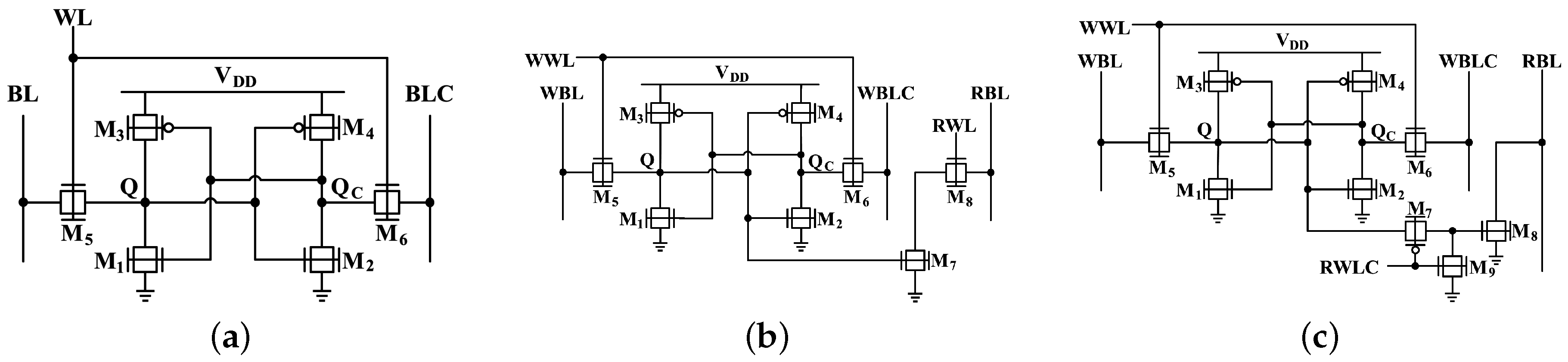
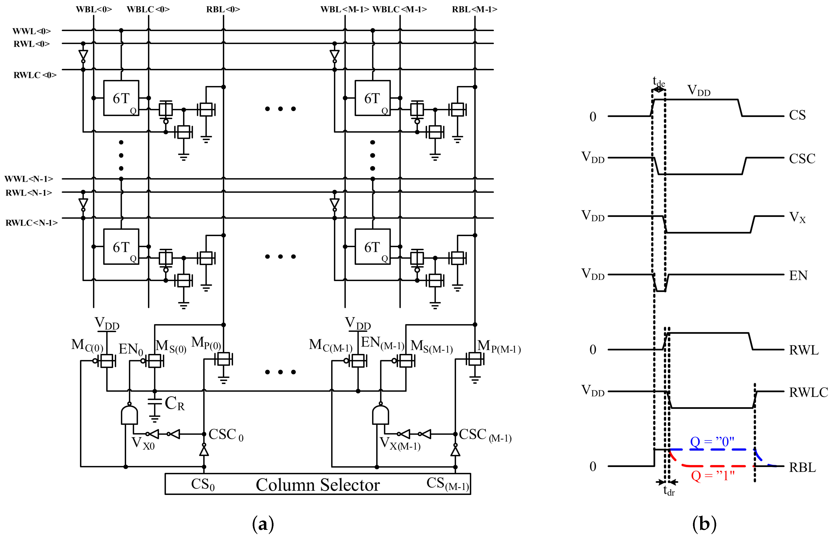
2.4. FinFET-Based SRAM
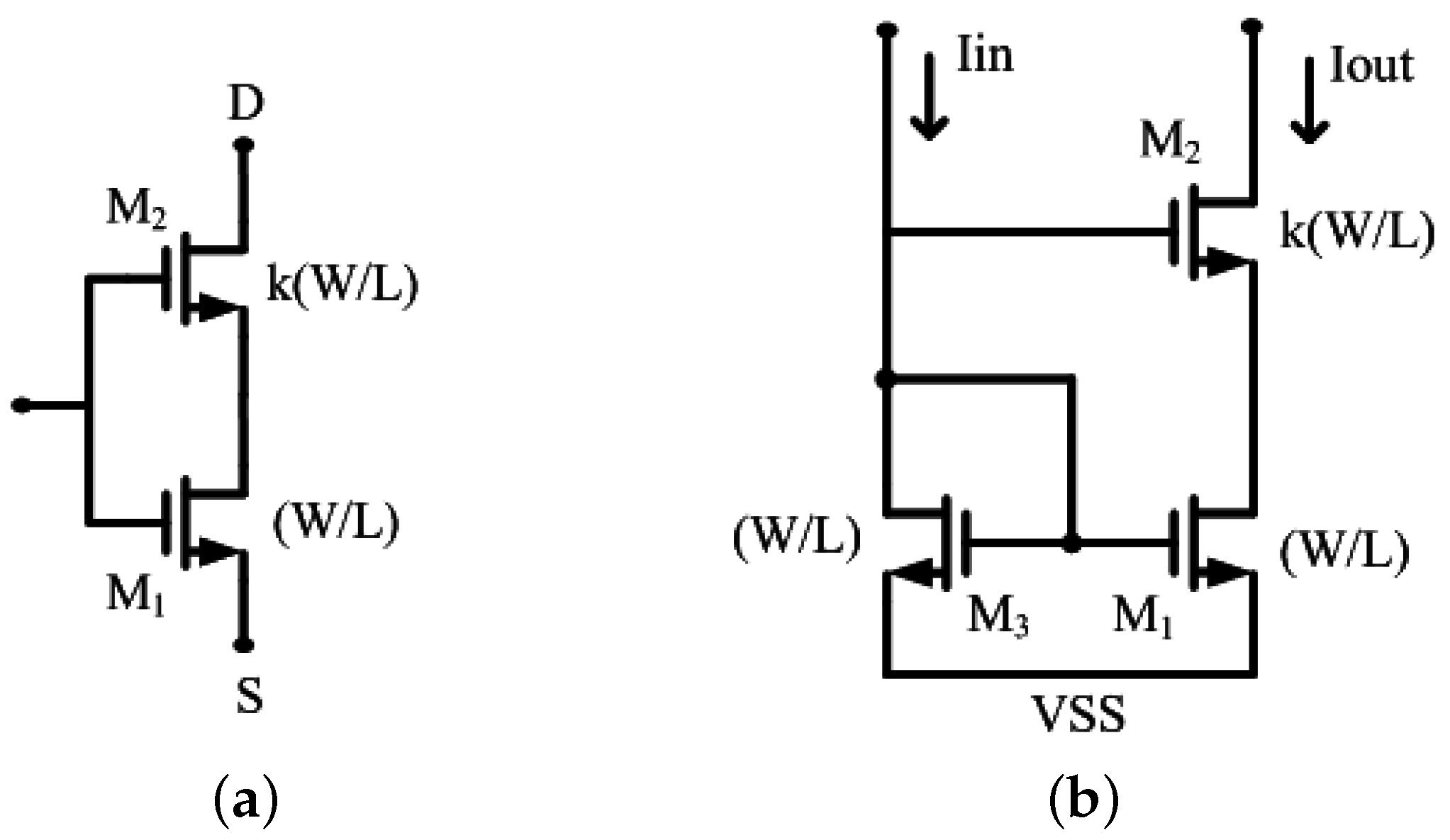
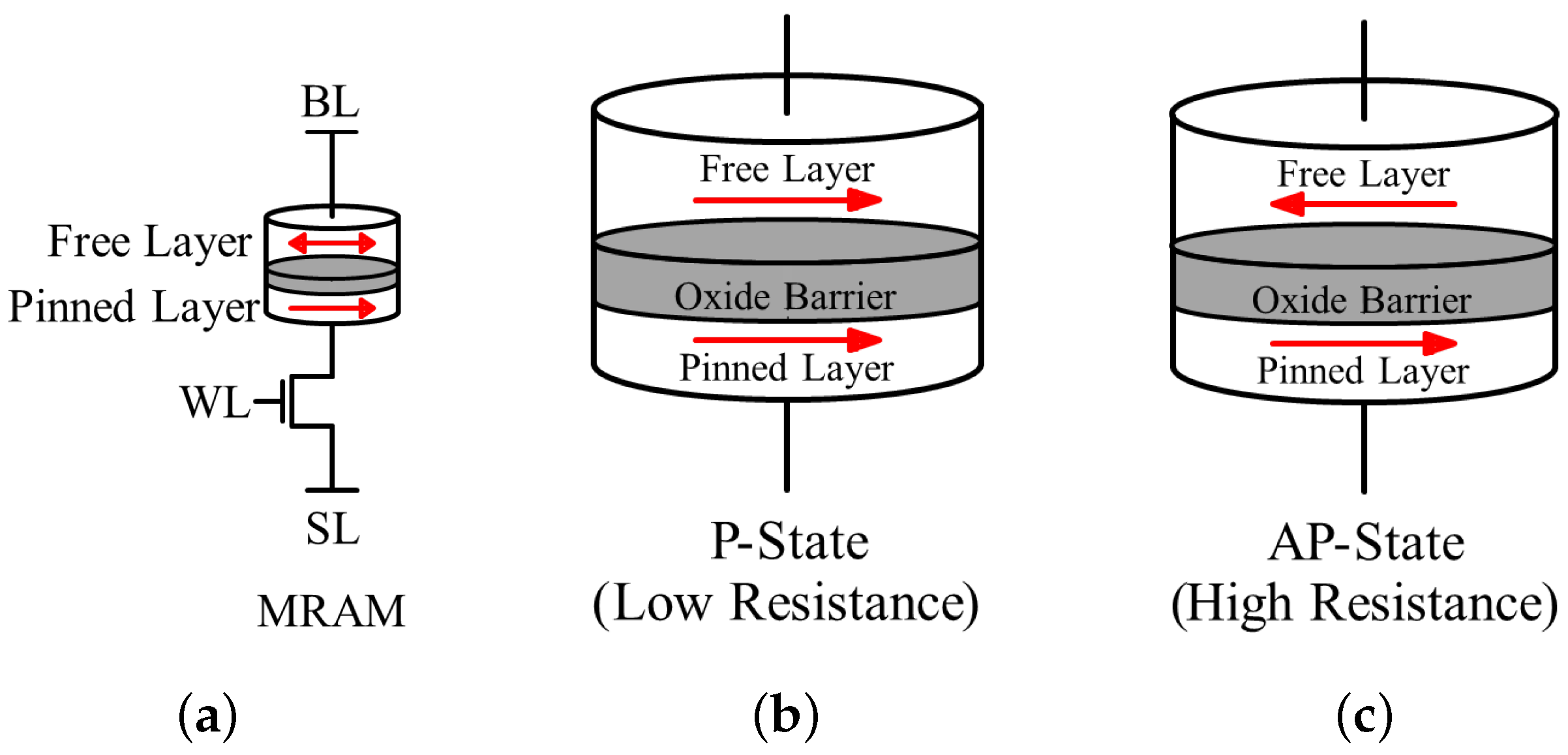
The efficiency of the FinFET technology is evaluated at the circuit level by exploring SRAM cells. SRAM arrays play an important role in future wearable and implantable electronics due to the requirement of larger on-chip memory with low leakage and high robustness. The robust operation of FinFETs at low supply voltages has enabled designers to implement low to medium frequency applications in a low power mode. However, all functions of an SRAM such as read, write and hold margins will be affected by increased process variation at low supply voltages (e.g., near or sub-threshold regions) which has degraded the yield. To improve the performance of the SRAM cell at ultra-low supply voltages, several FinFET SRAM solutions from device level [13] to circuit [17,18,19] and architecture level [20,21,22,23,24] have been proposed. However, most of these architectures suffer from degraded access time, especially at near/sub-threshold regions. To alleviate these obstacles of scaling the supply voltage to subthreshold voltages, the authors proposed a novel 9T-SRAM cell by which access time is reduced significantly while the read and write operations are not degraded [25].
The standard 6T-SRAM cell shown in Figure 4a consists of a cross coupled inverter latch and two access transistors controlled by word-line (WL) signals for write and read operations. The 6T-SRAM cell cannot operate at very low supply voltages, i.e., near/sub-threshold, due to the exponential dependence of the sub-threshold current to the threshold voltage of the transistors [26]. Furthermore, the window of transistor sizing is reduced due to the width quantization of the FinFET device. Therefore, it is not enough to only look at sizing consideration in order to achieve a robust operation in the near/sub-threshold region. To achieve a more reliable read operation, one solution is to use a buffer and exclusive read bit-line (RBL) and word-line (RWL) in an 8T-SRAM cell shown in Figure 4b. Due to the stacked n-FinFET transistors in the read path (i.e., M7 and M8), the effective overdrive voltage is reduced at low voltages and hence the access time is significantly degraded. This results in read failure at sub-threshold voltages. Furthermore, the operating supply voltage of the standard 8T-SRAM cell is also limited by the access time, which again is limited by the drivability of the transistors M7 and M8. To deal with these issues with respect to reducing the supply voltage, the 9T-SRAM cell is proposed with a 40% improved access time by removal of the stacked configuration in the read path.
In the 9T-SRAM cell (see Figure 4c [25]), the inverted read word-line (RWLC) is applied to the gate of a p-FinFET transistor (M7) which functions as a switch to connect the storage node to the gate of transistor M9. When the stored data is “1”, M9 turns on and the bit-line capacitance is discharged through the transistor M9. When the data is “0”, the transistor M9 stays turned off and the bit-line voltage change depends on the OFF current of the transistor M9. Furthermore, M8 is utilized to ensure that M9 remains OFF when the RWL is at “0”.
The performance of the proposed circuit during the read cycle is directly dependent on the voltage stored at the gate of M9. During read operation, the parasitic capacitance at this node can be charged very fast. This is performed through transistor M7 and the pull-up transistor in the cross coupled inverters (M3). When the stored data is “0”, since the parasitic capacitor at this node is discharged during hold state, the gate voltage of M9 remains at “0”. In this cell, the RBL cannot be precharged to V D D during hold mode since the leakage current will considerably increase due to the use of a single n-FinFET transistor in the read path. Hence, in the SRAM architecture, the RBL is discharged to the ground during hold and write modes to reduce the leakage current. However, the voltage on RBL needs to be at V D D at the beginning of a read cycle. To this end, a technique shown in Figure 5a is utilized by which the leakage current through the read path transistor M9 is reduced without any penalty on access time. The timing of the proposed technique is sketched in Figure 5b. By the use of this technique, the RBL is kept discharged through an n-FinFET transistor (M P ) during hold mode while, the capacitor ( C R ) which can be shared between all the bit-lines, is charged through a p-FinFET transistor (M C ). After asserting the column select (CS) signal, the enable signal (EN), which connects the capacitor to the bit-line, is generated. After asserting the EN signal, C R shares its charge with bit-line capacitance immediately and then becomes disconnected from the bit-line after a delay equals to the delay of 3 inverters ( t d e ). Afterwards, RWL is asserted and RBL either is discharged or keeps its charge after required delay ( t d r ) for generating the RWLC signal. This delay is equal to one inverter delay ( 60 ns at V D D = 0.27 V ).
To show the efficiency of the 9T-SRAM cell in comparison to the 6T and 8T cells, the performance of the cells in the presence of process variation and device mismatch is studied by the use of Monte Carlo simulations with 1000 samples. The proposed cell is realized by using the 14 nm FinFET technology. The Monte Carlo simulation for 14 nm FinFET technology includes the variations of L g , W f i n , H f i n , EOT and gate work function. For all the L g , W f i n , H f i n and EOT, the value of 3 σ is equal to 10% of the nominal physical value. The value of 3 σ for the gate work function parameter is 30 meV . To lower the leakage current and lower process variations, high- V t h transistors are used in the simulations. In the simulations, the 6T-SRAM cell is sized as follows: the access and pull-up transistors are implemented using one fin while the pull-down transistors (M 1 and M 2 ) utilize 2-fin transistors. In the 8T-SRAM, only M 7 uses 3-fin FinFET transistor while the rest of the transistors in the cell use 1-fin transistors. The proposed 9T-SRAM cell uses only 1-fin transistors. The different static and dynamic features of the 6T, 8T and 9T cells at V D D = 0.27 V are tabulated in Table 2 where the value of C R is chosen 1 pF at V D D = 0.27 V .
Based on Table 2, the variation of Read Static Noise Margin (RSNM) for the 8T and 9T cells is less than that for the 6T-SRAM. That is mainly due to the use of a buffer in the read path isolating the RBL from the storage point. During the write operation, the transient voltage collapse write assist technique [24] is applied to all SRAM cells to improve the write operation mainly due to this fact that the Write Margin (WM) of the cells is degraded significantly at sub-threshold voltages. The WMs of the 8T and 9T cells are higher than the 6T cell’s for sub-threshold region that is attributed to the use of 2-fin pull-down transistors in the 6T-SRAM cell. The 2-fin pull-down transistors increase the point which the storage nodes are flipped. It makes the pull-up transistor stronger while the access transistors become weaker.
To calculate the access time, a 70 mV bit-line voltage difference from V D D is considered to be sensed by a sense amplifier (SA). Access time is defined as the time required for discharging the bit-line to a sensible voltage for the SA after asserting the RWL. During the write operation, the time between asserting the word-line signal and when the storage node voltages cross 90% of their final values is measured as write time. According to the simulation results, the access time of the 9T cell is 40% shorter than as for the 8T-SRAM at V D D = 0.27 V . Furthermore, the write time of the 9T cell is improved in comparison to the 8T-SRAM cell at V D D = 0.27 V that is attributed to the use of a 3-fin pull-down transistor in the read path of the 8T cell. This 3-fin transistor increases the parasitic capacitance of the storage node and hence increases the write time. In the case of the standby power, the proposed SRAM cell provides the lowest leakage current in hold “0” in comparison to the 6T and 8T cells.
On the other hand, the leakage current of the proposed SRAM increases in hold “1”, which is mainly due to the leakage current of M 7 . All of the mentioned improvements are achieved at the cost of an 82% and 15% area overhead compared to the 6T-SRAM and 8T-SRAM cells, respectively.
According to above simulation results, although the 9T-SRAM improves the performance of the memory, we have to come with new solutions and memories to further reduce the power consumption while the performance of the memory is preserved. In this respect, we briefly describe Spin Transfer Torque RAM (STT-RAM) which is one of the promising candidates to replace the SRAM as a universal memory.

2.5. STT-RAM

The STT-RAM is a promising candidate to replace the SRAM cells due to its unique features including non-volatility, low leakage, long endurance, CMOS-compatibility, and high-speed access [27]. The STT-RAM cell consists of a Magnetic Tunnel Junction (MTJ) in series with an access transistor, which is controlled by the WL signal. The MTJ is composed of two magnetic layers, i.e., pinned layer and free layer, and one oxide barrier layer as shown in Figure 6. MTJ resistance is defined by the relative magnetization direction of two ferromagnetic layers. When the magnetization directions of magnetic layers are parallel (P-state) or anti-parallel (AP-state), MTJ resistance is in low or high states, respectively. Thus, the MTJ can be used as a binary memory cell (low resistance ( R L ): logic “0”—high resistance ( R H ): logic “1”). The process of parallelizing the free and pinned layers is more efficient than the anti-parallelizing process. Besides, according to Figure 6a, write currents are significantly different. When current flows from the bit-line (BL) to source-line (SL), the gate-source voltage of the access transistor is equal to V D D since the transistor source is grounded. It results in an overdrive voltage of V D D - V t h . However, when the current flows from SL to BL, the overdrive voltage of the transistor is considerably degraded because the MTJ functions as a source degeneration resistance in this scenario. Furthermore, the body biasing effect increases the threshold voltage of the transistor and further degrades the write current.
The above described phenomena result in an asymmetric write operation in the STT-MRAM cell. The write operation is also a stochastic process and altered during time, even when the operating and environmental conditions remain the same [27]. The switching possibility is improved by extending the write pulse period (i.e., duration of write current), hence the write failure probability is reduced. On the other hand, increasing the switching current can decrease both mean and variation of the switching time, which also helps to reduce write failures. However, this approach occupies a larger die area in an STT-MRAM cell, decreasing the memory density. In order to solve this issue, several assist techniques have been proposed to reduce the write time and power consumption. For example, in [28], a negative voltage is applied to the BL during write “1” operation to improve the drivability of the access transistor. Furthermore, in [29], an external magnetic field is applied to MTJ to facilitate the switching process leading to the critical current reduction. Other methods have been proposed which monitor the data in the cell and terminate the write operation immediately after switching [30,31,32,33]. However, all these assist methods improve the switching process at the expense of extended area overhead and/or reliability problem.
At sub- 22 nm technologies, the performance and reliability of the STT-RAMs during read becomes challenging. In scaled technology nodes, read disturbances increase mainly due to the scaling of the critical current, I C . The read disturbance of the STT-RAMs is caused by the same current paths for read and write. The read current should be sufficiently lower than I C to avoid any disturbance during read operation. Although a small read current alleviates the read disturbance, it will reduce the read margin, which considerably increases read failure probability. The read margin is defined as the difference between the BL voltage and reference voltage, and a good design with large read margin is required due to the small Tunneling Magnetoresistance Ratio (TMR) of the available MTJ technologies. To deal with this issue, self-reference read scheme has been proposed, which compares the original resistance state of the MTJ to a reference resistance provided by the same MTJ [34,35,36]. Such techniques can be categorized mainly into destructive and non-destructive sensing schemes. In destructive schemes, the original data is destroyed when the reference value is written into the MTJ. Therefore, it will result in a high power consumption and a longer access latency due to writing back the original data into the MTJ. Besides, since the process of writing back the data may not complete, it can degrade the reliability of the device. On the other hand, the non-destructive approaches preserve the data into the cell while they suffer from the degraded sensing margin in more scaled technology nodes.
In general, CMOS scaling provides the benefits of higher speed, lower power consumption and denser area for digital and memory circuits. However, the reliability and the leakage power become challenging issues in scaled CMOS technology. To deal with these obstacles, alternative devices such as FinFET and working in sub-threshold region can be recruited. However, we need to come up with new circuit and architecture level solutions to improve the performance of digital circuits in sub-threshold region. Furthermore, in memory design, the challenging SRAM cell can be replaced by the promising STT-RAMs. Although the STT-RAMs can reduce the area overhead and alleviate the leakage power, the read and write operations are challenging in scaled technology nodes.

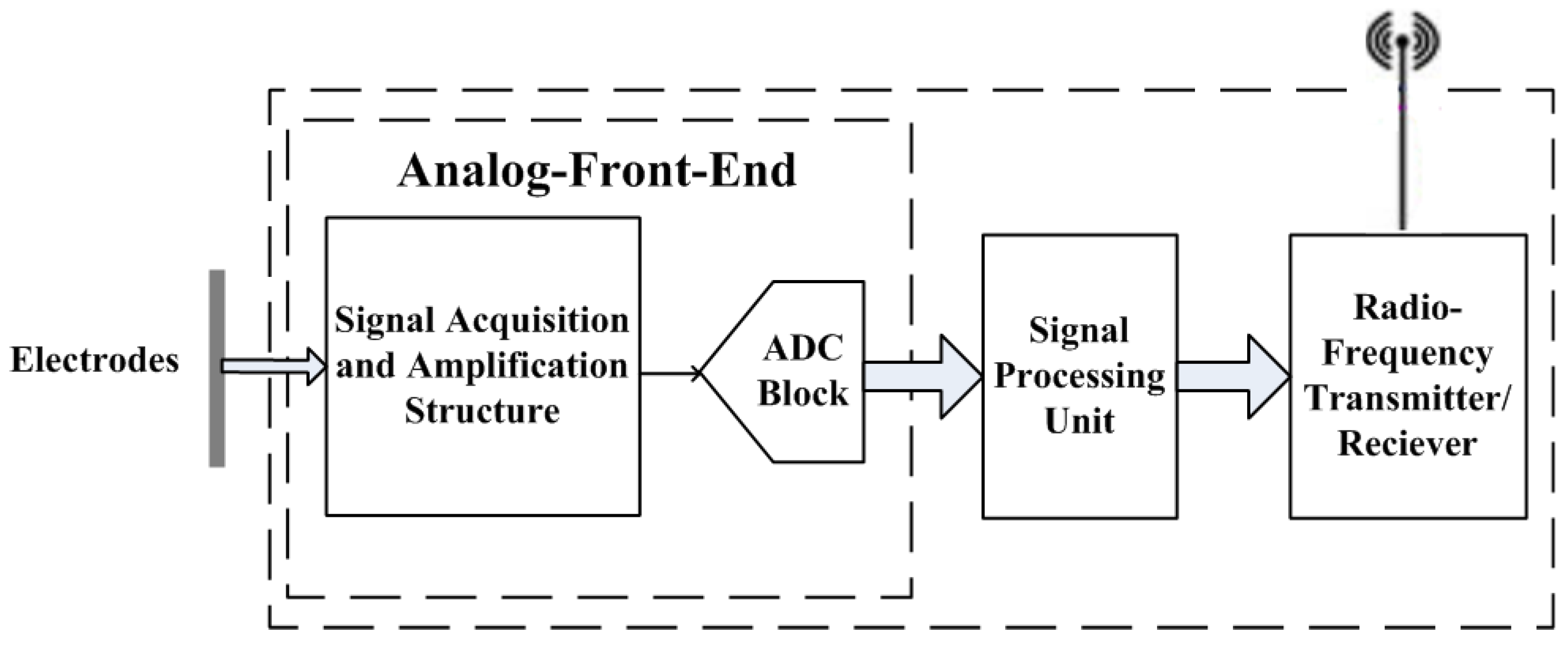
3. Low Power Analog Design

Unlike the digital circuits where the supply voltage scaling provides the most effective power reduction due to quadratic relationship to dynamic power, reducing the supply voltage does not lead to minimum power consumption when bandwidth and signal to noise ratio (SNR) must be preserved [26]. Besides, scaling of supply voltage reduces the linear range of analog circuits leading to a limited dynamic range (DR). However, scaling of the supply voltage has become a necessity mainly due to the trend of technology scaling. In the following section, some circuit tricks to design low voltage operational amplifiers (opamp), which is the most representative analog circuit, will be explored. Afterwards, since the main focus of the paper is on FinFET device as an alternative to replace CMOS technology, opamps realized in CMOS and FinFET technologies will be compared.

3.1. Low Voltage Design Techniques

Some applications, for instance bio-medical signal acquisition shown in Figure 7, need small currents and low supply voltage. The structure shown in Figure 7 can be utilized to acquire the electroencephalogram (EEG)/electrocardiography (ECG) signals where the EEG/ECG input signals are sensed with the electrodes. Then, since these signals have amplitudes in the lower voltage ranges, therefore an analog front end (AFE) structure is utilized to acquire and amplify the signals [37]. The amplified signals will be digitized by analog to digital converters (ADCs). Thereby, the successive approximation or sigma-delta ADC blocks can be utilized for decreasing the power consumption. After the digitization of the input signals, they will be fed into the signal processing unit to extract the epileptic features [38] and the output will be utilized to detect the onset of seizures by means of a machine-learning classifier that is trained to the patient-specific data [39]. In the final step, the outputs of the classifier (data) will be sent to an external device, such as a mobile phone or a server in a clinic [40].
In [41], a typical wireless EEG system is described. In this system, first, 18 channels are utilized for EEG signals recording and amplification. Then, after the digitization of the amplified EEG signals, the feature vector extraction is done locally and only the classification is performed remotely. Finally, the radio frequency transmitter used in this system is a commercially available low-power transmitter, ChipCon CC2550 [42]. As a result, by considering the actual measurements of the hardware prototype for 18 channels, the total power consumption of this system is about 120 μW.
At low supply voltages, scaling of threshold voltage can be considered as an alternative to improve the DR. However, similar to the digital case, the lower V t h reduces the noise margin and hence degrades SNR. On the other hand, many design techniques have been proposed for low voltage analog circuits which provide an acceptable noise and bandwidth specifications [43,44,45,46]. In low supply voltages, the analog circuits can be implemented in the sub-threshold region [43,44,47,48,49]. By considering the sub-threshold region, the drain-source current and transconductance equations are obtained as the following equations [26]:
I D = I D 0 W L e V G S n V T 1 e V D S V T .
g m = I D V G S = I D n V T ,
where n > 1 is a nonideality factor and V T = k T / q is the thermal voltage. From Equation (3), it can be seen that the transconductance in the sub-threshold region is larger than the corresponding in saturation region ( g m = 2 I D / ( V G S V t h ) ) mainly due to the exponential dependence of the drain current on V G S in the sub-threshold region. However, in the sub-threshold region, the bandwidth is limited. Therefore, using of the sub-threshold region is suitable for the applications in which the crucial specification is the power consumption not the speed.
By scaling the technology, the output impedence of the device is shrinking mainly due to channel length modulation. One solution is to cascade several low gain stages, but the stability problem will be aggravated. Therefore, in high gain opamp structures, the cascaded transistors at the output stages are utilized to increase the output impedance. However, due to the threshold voltages of the cascaded transistors, this structure cannot be utilized for low voltage regime. To deal with this obstacle, the self-cascode structure can be used in which the high output impedance is achieved in the low voltage design. As shown in Figure 8a, a self-cascode structure is a 2-transistor structure in which both of the transistors have the same gate bias voltages and the size of M 2 is considered k times larger than the size of M 1 [44]. Figure 8b shows the current mirror structure based on self-cascode MOSFETs. As depicted, M 1 and M 2 has the same DC current, but since the size of M 2 is k times larger than M 1 , the overdrive voltage of M 1 and the output voltage will be:
V o v e r d r i v e , M 1 = k 1 V o v e r d r i v e , M 2 ,
V o u t p u t = k V o v e r d r i v e , M 1 .
According to Equations (4) and (5), for k > 1 , the output voltage of the self-cascode structure has increased. Therefore, the self-cascode structure can be realized at the output stage of the op-amps in order to increase the output impedance in low voltage regime. Many techniques have also been proposed to settle challenging opamp designs in switched-capacitor circuits, which have gained importance in analog and mixed-signal designs. As mentioned earlier, low supply voltage leads to lower signal swing which requires a higher capacitance to maintain the same SNR by noise improvement. Higher capacitance imposes more power dissipation to achieve the same speed. To address the challenges, attractive solutions such as correlated level shifting (CLS) [45] and Comparator-Based (CB) opamps [46] have been proposed. In CLS, the error, emerging from finite opamp gain, is alleviated by sampling the output signal during an estimation phase and then improving the output signal by removing the error signal. This technique can provide a rail-to-rail operation leading to a higher SNR. The CB structure replaces the opamp with a combination of a comparator and current sources. This technique uses the fact that the opamp provides a virtual ground during the charge transfer phase in switched-capacitor circuits. Therefore, the comparator can be replaced to detect the virtual ground condition and enables the charge transfer phase. Both CLS and CB opamp structures can be utilized in low power high performance switched-capacitor analog and mixed-signal applications.
As mentioned above, CMOS circuits can be implemented in the sub-threshold region. For these circuits, the reference voltage decreases as well as the supply voltage that is reduced below the threshold voltage [50,51]. Implementing CMOS circuits in subthreshold region requires designing accurate voltage regulators as well. In literature, some works [52,53] have shown implementations of voltage references using MOSFETs operating in sub-threshold region. However, the main problem of these circuits is the variation of the reference voltage followed by process variations. Therefore, in [54,55], the resistive dividers are utilized to achieve the output voltage below the threshold voltage. But, lower currents require large resistors which enlarges the area. Recently, some voltage reference circuits [56,57] have been implemented based on two devices with different threshold voltages. In these circuits, the output voltage is obtained according to the threshold voltage difference of two transistors. However, the process variation and the specific process technologies limit the use of these voltage reference circuits. In [58], another voltage reference circuit, based on the switched capacitor technology and the body effect in MOSFETs, is introduced. In this circuit, the output voltage is obtained as the difference between two gate-source voltages using only one PMOS transistor operated in the sub-threshold region. This reference voltage circuit has low sensitivity to the temperature and consumes nano-power.

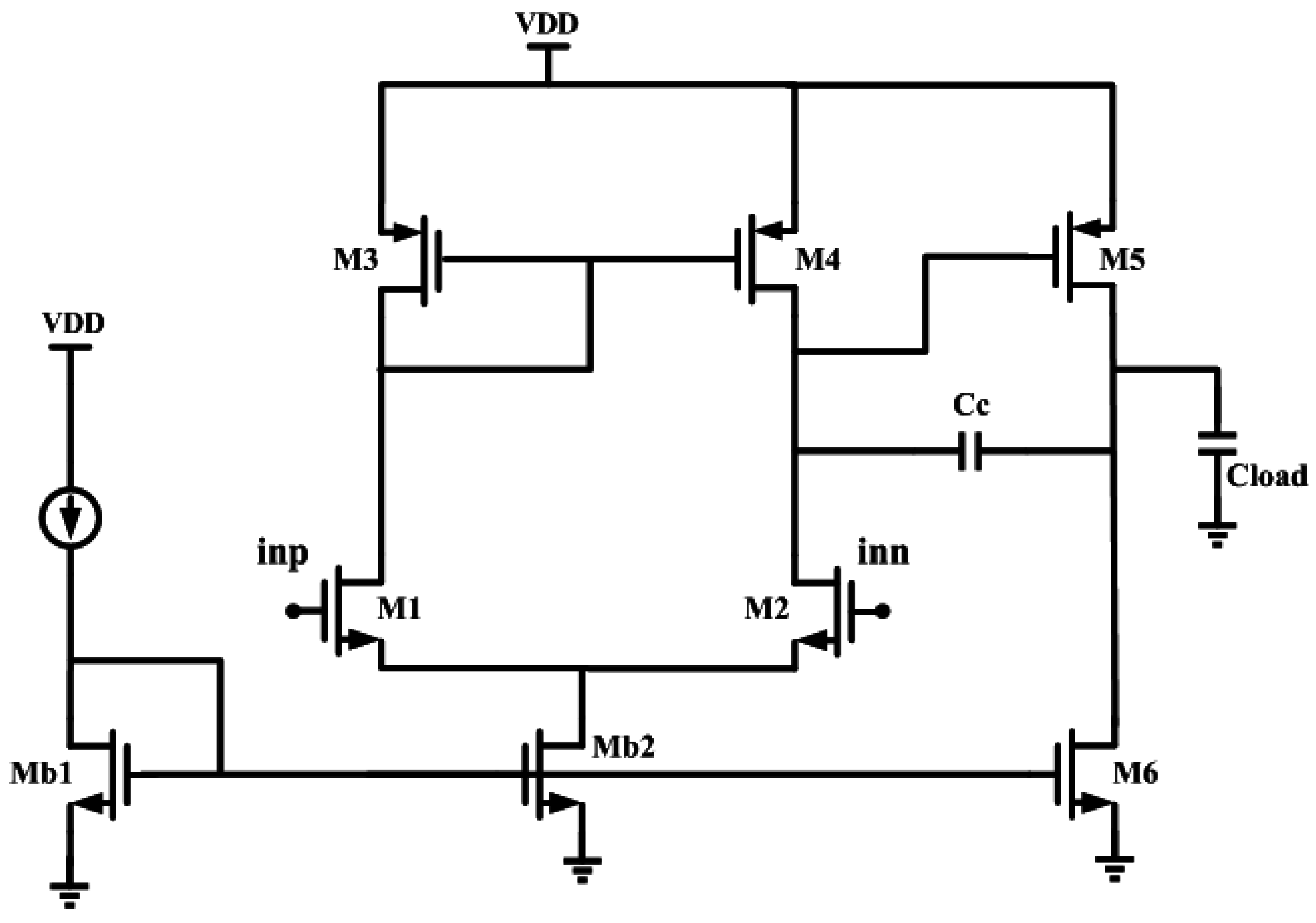
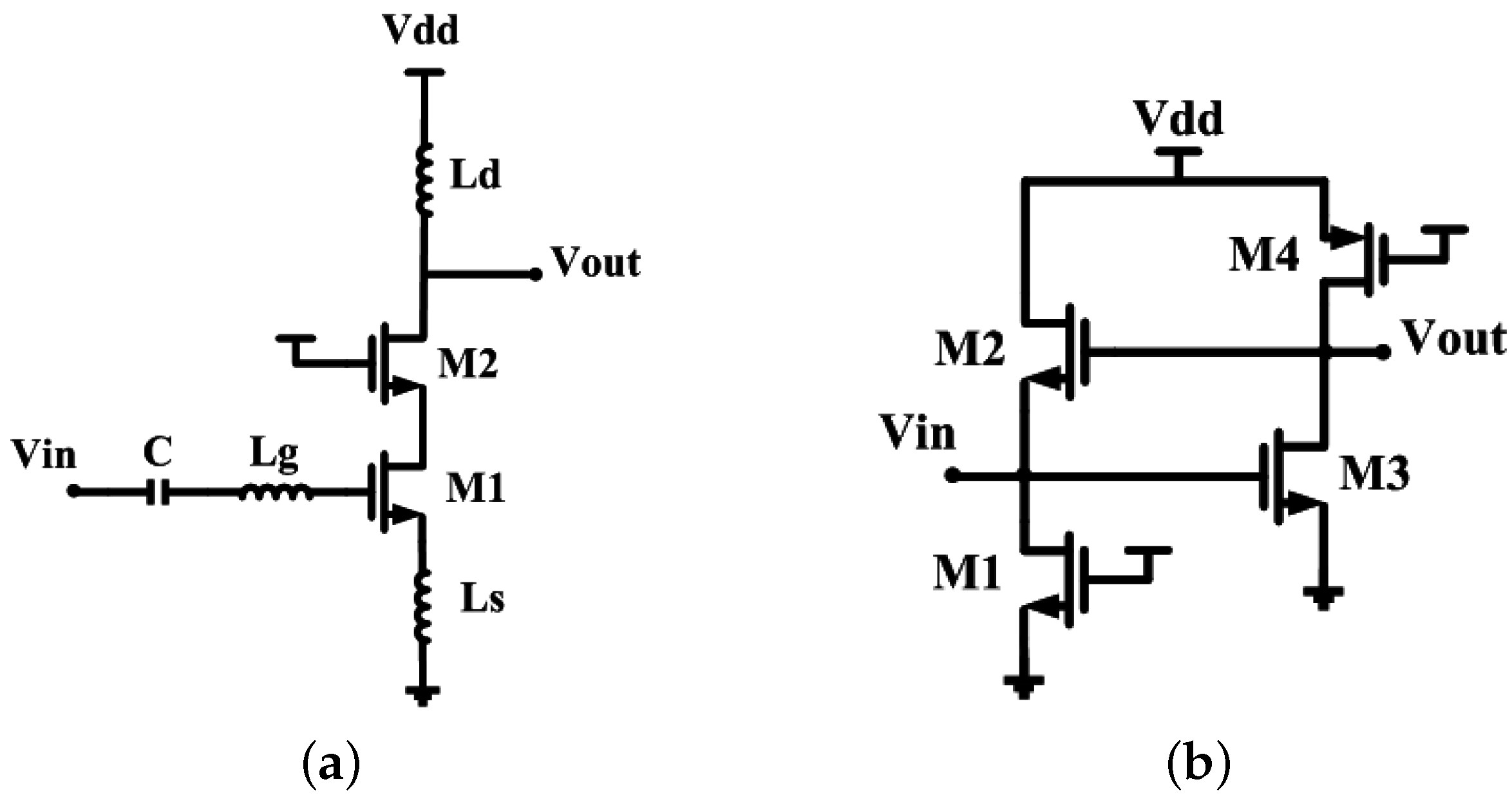
3.2. Analog Cells in FinFET Technology

As mentioned previously, the FinFET technology is currently utilized by digital designers for low voltage and low area applications because of the superior energy efficiency with respect to standard MOSFETs. Today, most electronic chips and circuit implementations include both digital and analog structures in combination with each other. Therefore, using the FinFET technology for analog circuits is essential as well, so the entire chip can be fabricated using the same technology.
Due to the better electrostatic characteristics of the FinFET, higher intrinsic gains are obtained in more power efficient ways. However, the main challenges of the FinFET device are the higher parasitics derived from source resistances and extrinsic capacitors [59] and the quantified width of the device.
To evaluate the performance of the FinFET in analog designs, a two stage opamp structure, showed in Figure 9, is designed in 14 nm FinFET and 65 nm CMOS technologies.
It should be noted that the mentioned 65 nm CMOS technology is based on the TSMC PDK model. In this comparison, the different results of two technologies are obtained according to one specific goal. Therefore, the simulation results have been extracted based on the same phase margin of 60 and listed in Table 4. By this condition, the DC gain in 14 nm FinFET devices is 10 dB more than the DC gain in 65 nm CMOS technology. Also, the power consumption has been decreased from 416 μ W in 65 nm CMOS technology to 180 μ W in 14 nm FinFET technology, as was desired. Furthermore, as shown in Table 4, the unity gain bandwidth of the 14 nm FinFET technology ( 338 MHz ) is higher than the unity gain bandwidth of the 65 nm CMOS technology ( 125 MHz ). (It should be noted since the 16 nm CMOS technology is not available for us, we have compared the two analog circuits in the 14 nm FinFET and 65 nm CMOS technologies. But, since this 65 nm CMOS technology is based on the real TSMC PDK model, the obtained results are more accurate than the results achieved by comparing the 14 nm FinFET technology and 16 nm CMOS technology which is not based on the real TSMC PDK model.)
The main features of implementing the radio frequency (RF) CMOS circuits such as low noise amplifies (LNAs) are their gain, speed, power consumption and noise. As mentioned in [60], FinFET devices achieve higher gain in comparison with the planar CMOS devices. However, the specific speed ( f T ) is higher in planar CMOS devices compared to the FinFET devices. Furthermore, as mentioned above, FinFET devices are very power-efficient in comparison with the planar devices. In addition to the gain, speed and the power performances of the RF design using planar and FinFET devices, noise is an important performance feature as well. As depicted in Figure 10 and mentioned in [58], the noise figure (NF) of the inductive LNAs is proportional to f 0 / f T , where f 0 is the operating frequency. Furthermore, the NF of the feedback-based LNA is proportional to 1 / g m [58]. Finally, by considering the same current consumption for both FinFET and planar devices, it is evident that since the FinFET devices have higher parasitic capacitance derived from source resistances and extrinsic capacitors [59], the FinFET devices have lower f T and higher noise in comparison with the planar devices. As a result, device optimization will be required to decrease the parasitics and improve the performance of the FinFET devices for RF applications [61]. As an example described in [60], by consuming similar power (10 mA ), the FinFET LNA devices achieve lower bandwidth (2 GHz ) and higher NF because of their higher parasitics in comparison with the planar devices with a bandwidth of 2.5 GHz , and a low NF of 2.6 dB . In summary, although the planar devices provide lower gain in comparison with the FinFET devices, their speed and noise performances are more appropriate for RF applications.

4. Energy Harvesting

Reducing the energy cost of running an electronic system can enable us to use energy harvesting as a power source. This opens up for a whole range of new applications both in terms of distributed wireless networks in rough environments, where it is not possible to access the sensor node by wires or change batteries, or in implanted sensors where size and bio compatible requirements makes it impossible to attach a battery. Instead, different energy harvesting techniques makes it possible to harvest ambient energy from the surroundings and continuously power the system.
In this section, we will look at the feasibility of powering a system using only energy harvesting techniques and discuss the advantages and disadvantages of some of the more popular methods and certain combinations of harvesters.

4.1. Techniques and Sources

There are a variety of energy sources available in the environment such as light from the sun or indoor lighting, electromagnetic waves from cell phones and WiFi connections, vibrational energy from engines and buildings, wind power, wave energy, waste heat etc. The human body is, in itself, also an incredible source of power, both in terms of mechanical movement and vibrations when we move or talk, continuous stream of blood flow, excess heat, bio-chemical energy from physiological processes, etc. All these power sources can be harvested by kinetic harvesters, fuel cells, solar cells and thermal harvesters. The kinetic harvesters are mainly comprised of piezo electric and troboelectric harvesters, electrostatic transduction and magnetic induction generators. A good review of the most popular harvesting techniques was done by J. Olivo et al. [62]. It was found that the power income of harvesters was: kinetic; 40 μW–80 μW, thermoelectric; 1 μW–30 μW, fuel cells; 2 μW–430 μW and inductive links; 0.14 mW 150 mW , respectively.

4.1.1. Solar Energy

Solar energy is an abundantly available and exploitable energy source outside and has been thoroughly researched for decades in the pursuit of producing even higher energy conversion efficiencies. Solar cells have developed into 5 main categories, crystalline silicon, thin film cells, organic/polymer, hybrid PV cells and dye-sensitized cells to fit a variety of applications, ranging from big solar power plants to small wearable devices. Crystalline silicon is one of the original cell types and is advantageous because of the easy availability and good efficiency (21%–28%) [63]. However, the manufacturing costs are significant, so cheaper alternatives, such as thin film cells, where less material is needed, are explored. Thin film cells come in a range of different technologies (amorphous, CdS/CdTe, CIS/CIGS) [64], with efficiencies ranging from 11%–29% [63], with the lowest efficiency being the recently emerging quantum dot technology. In 2014, a new efficiency record at 46.5% of a multi-junction concentrator solar cell, was presented by Tibbits et al. [65]. However, the usefulness of this multi-junction type is limited by the high fabrication cost and, for some applications, the inflexible structure. In stead, organic cells and dye sensitized cells are showing great potential because of the low fabrication cost and for the organic cells; low environmental impact, wide tunability of chemical functionalities and good compatibility with flexible substrates that makes them a great candidate for wearable/implanted devices. The maximum lab efficiencies ranges from 5%–11.5% with the best performance given by the dye sensitized [63,66,67,68]. A more detailed overview of the top lab efficiencies is provided by NREL [63] (National Renewable Energy Laboratory (NREL) www.nrel.gov).
With a typical spectral irradiance of 1000   W / m 2 on a surface illuminated by the sun at the AM1.5 standard, the power produced by the solar cells in the efficiency range of 5%–45% is 5 mW / cm 2 45 mW / cm 2 . If the device is operating indoor, the spectral irradiance depends on the light source and the solar cell efficiencies also depend on how the bandgap energies match the light source. However, a typical range of irradiation is 0.05 mW / cm 2 5 mW / cm 2 [69] and if we consider the worst case scenario, the corresponding converted power outputs in the same efficiency range are 2.5 μW/ cm 2 –22.5 μW/ cm 2 .
An example of an autonomous bio implant that is powered solely by solar energy is an implantable intra ocular pressure monitor done by Ghaed et al. [70] in 2013. The low power techniques utilized are ultra high threshold voltage and thick gate oxide to keep the leakage power low in the capacitance to digital converter. The SRAM is a 10T cell that uses gate length biasing in the dataretaining portion while power gating the read buffer to acheive 2.4 fW / bit standby leakage [71]. The V D D is scaled down close to the minimum energy point so the micro processor and SRAM consume only 90 nW combined at 0.45 V in active mode. The entire system including a capacitive MEMS pressure sensor, capacitance to digital converter, transceiver, SRAM, μP and SCVR is powered by a 0.07 mm 2 solar cell that produces between 13 nW and 80 nW in bright indoor and outdoor sunny lighting respectively. This corresponds to a power output of 0.02 mW / cm 2 0.11 mW / cm 2 , which is significantly less outdoor than what is stated above, however, it must be noted that this system is implanted in the eye and therefore never subjected to direct sunlight and significant absorption of some wavelengths is expected. The system is nevertheless able to measure the intra ocular pressure every 15 min and transmit the data once a day with only 1.5 h of sunlight or 10 h of indoor lighting per day.

4.1.2. Mechanical Energy

Mechanical energy is the most widely distributed energy source and it is a source that fits well with the area of IoT that includes human-related motion applications. An extensively researched technique to harvest mechanical energy, is using piezoelectric and triboelectric materials because of the possible applications in flexible and wearable electronics. Other techniques such as magnetic induction or electrostatic transduction have also been used extensively in the past, however, with the recent trend in comfortable, flexible and compact wearable devices, the piezoelectric and triboelectric materials show most potential in flexible materials that are functional, cheap and easily industrially available.
The most common materials used are ZnO, lead zirconate titanate (PZT), poly (vinylidene fluoride) (PVDF), 2D materials and composite materials. PZT is a widely used ceramic material with high dielectric constant and piezoelectric voltage, but it is also brittle and can only withstand a maximum safe strain of 0.2% [72]. Generators such as piezoelectric nanogenerators (PENGs) and flexible triboelectric nanogenerators (TENGs) have been extensively researched since the first ZnO nanowire-based generator was demonstrated in 2006 [73]. TENGs are simple and cost effective and the maximum power output of a triboelectric nano-generator has reached 50 mW / cm 2 [74] and an energy conversion efficiency of 70.6% [75]. This means that it can also be used to harvest energy on a large scale, like wave or wind energy. However, a typical flexible polymer TENG for wearable applications yields a power density of 10.4 μW/ cm 3 [72]. For biological applications, the polymer-based piezoelectric materials, PVDF, is advantageous because of the chemical resistance of polymers, the ease of fabrication, flexibility and bio-compatibility. The disadvantage is that in order to achieve good performance, the material must be electrically poled first [72].
In order to track and convert motion energy from humans without the uncomfortable feeling of having to bend something when you move, piezoelectric fibers have been developed [76]. They have proven to be bent and folded repeatedly without any damage and they can produce an output power of 60 nW at 1.5 V with a bending frequency of 2 Hz . Furthermore, arrays of these fibres have excellent pressure response at small values ( 0.1 Pa at low pressures) so they can work excellently as pressure sensors. For smart clothing application, fibers have been coated with nanowires by Lee et al. and woven to a fabric using the “brush-to-brush” fabrication model, where the nano wires brush up and down against each other and generates electricity from slow movements (<1 Hz). This results in a power density of 16 μW/ cm 2 [77].
Implanted sensors and actuators powered by piezoelectric materials can also be realized by powering them externally using ultrasonic waves. This power transfer option is often the better choice when dealing with very small and deeply implanted sensors. In Figure 11, an overview of power outputs from RF, near-field (typically inductive) and ultrasonic sources is shown. The figure shows the general trend that RF is relatively low power outputs and best for near-surface implants, near-field gives high power outputs for near-surface implants, but is relatively large and ultrasound gives high power outputs even for deeply implanted small sensors.
When implanted sensors and actuators are powered externally using ultrasonic waves, the pressure wave from the ultrasound will force the piezoelectric material to stretch and compress and an AC current will be produced. An example of a device, powered by ultrasonic energy transfer, was demonstrated by Charthad et al. 2015 [91]. The device is a 4 mm × 7.8 mm implant including an IC with a 2 nF on-chip storage capacitor, a hybrid data link consisting of a ultrasonic downlink and RF uplink. The system can support a load of 100   μ W and the total power consumption of the IC is 85   μ W , which is far more than the previous example of a solar powered implant, however, by using ultrasonic power, the available power is also much higher. The system is powered at a distance of 3 cm in chicken meat by a 0.36 mW / mm 2 ultrasonic wave, which is 5% of the FDA limit. The dimensions of the ultrasound piezoelectric receiver is 1 mm × 1 mm × 1.4 mm .

4.1.3. Combinations of Energy Harvesters

A combination of energy harvesters can be useful for cases where multiple energy sources can provide a comparable amount of energy to boost the total harvested power. It can also be advisable when the harvesting circuits requires initial power to harvest energy. This is, for instance, the case for highly efficient solar harvesters where the energy must be harvested at a specific voltage for optimum efficiency.
Flexible hybrid nano-generators (FHNGs) have been developed to harvest multiple types of energy sources that complements each other in an effective manner. The challenge here is to choose suitable materials with good flexibility, compatibility and mechanical stability and develop fabrication methods that are applicable to the industry.
An example of a FHNG with harvesters that complements each other is the combination of PENG and TENG by Jung et al. [92]. Here, the high piezoelectric current output and the high triboelectric output voltage is powering simultaneously in one operating cycle. The combination produces a peak voltage of 370 V , a current density of 12   μ A / cm 2 and a power density of 2.04 mW / cm 3 . The device can successfully power 600 LEDs by the force of fingers (≈0.2 N).
Because the voltage level of indoor operated solar cells becomes comparable to PENGs voltage output, it is also a good design to use both PENGs and solar cells together. A combination of an organic solar cell in co-junction with a ZnO piezoelectric material is developed by [93]. The device is a combination of several flexible layers, including Indium tin oxide as cathode for the solar cell, and the average power conversion efficiency of the solar cell was 1.5% with an open circuit voltage and current density of 0.55 V and 9.2 mA / cm 2 in standard AM 1.5 illumination respectively. However, the indoor photovoltaic voltages ranged from 10 mV to 120 mV which fits well with the piezoelectric voltage that was up to 150 mV and an output current around hundreds of nA [93].
Even a triple combination of a thermal, solar and mechanical energy harvesters have been fabricated by Yang et al. [94].

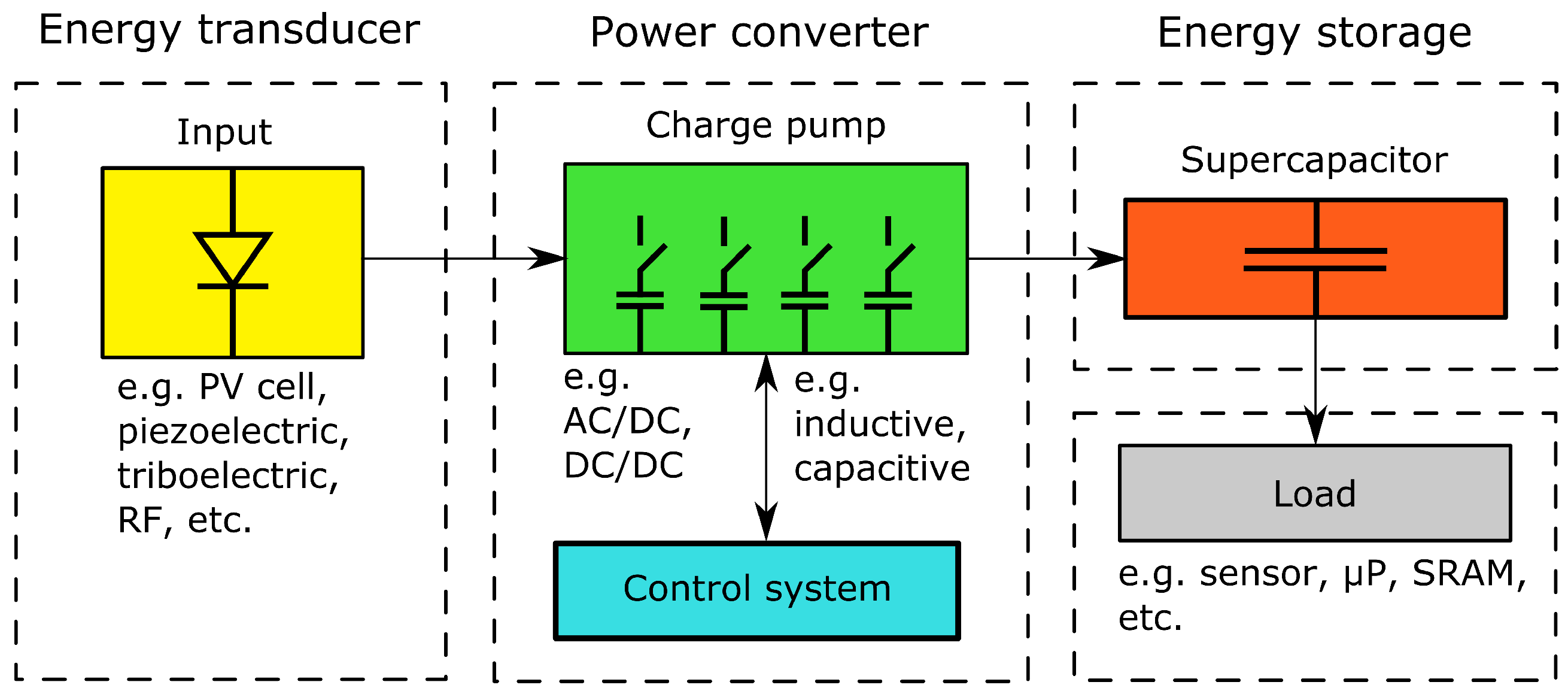
4.2. Energy Harvesting Interfaces
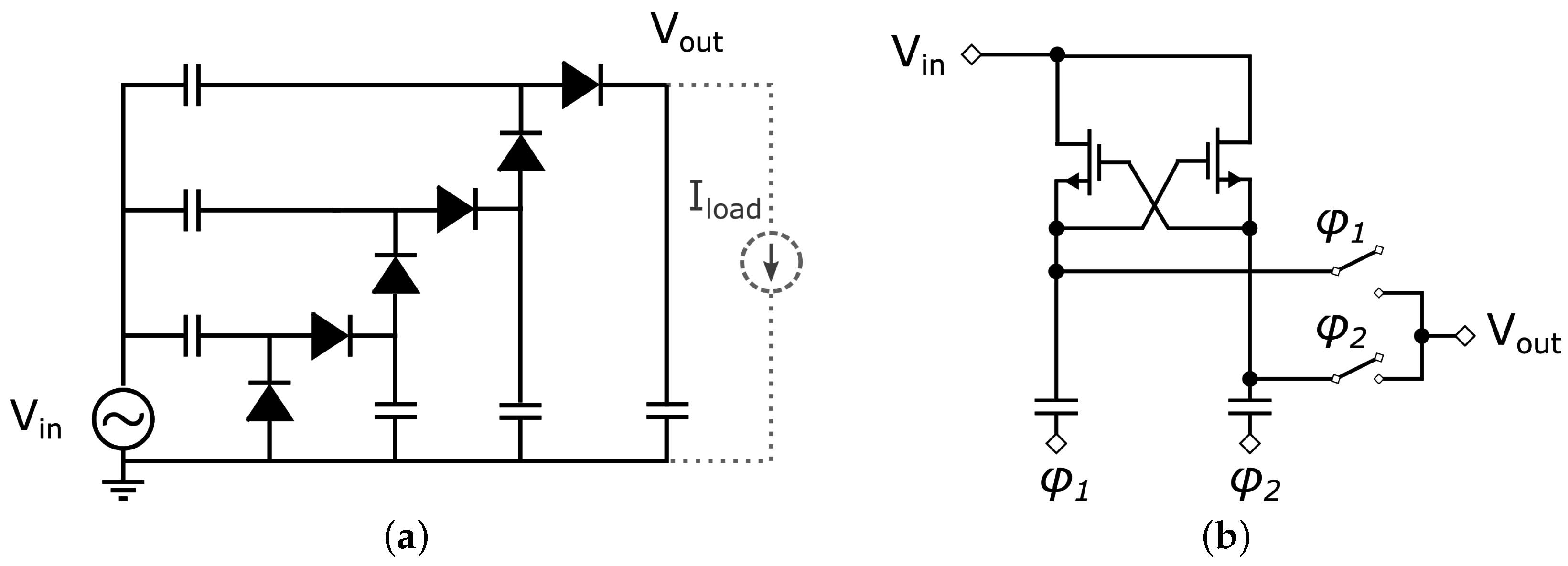
When designing an energy harvesting system (see Figure 12), the transducer (energy harvesting unit) is usually not suitable to power the loads directly because of the often low input voltage and varying nature of the ambient energy sources and thus the power input level. Therefore the energy is transferred directly to a power converter that upconverts the voltage to the desired level and then charges the energy storage or buffer that powers the load. Architectures have also been made where a control system directs the power directly to the load, bypassing the energy storage, when there is enough ambient energy, thus saving energy by not having to charge and discharge the energy to the storage unit [95]. The energy storage is usually implemented using super-capacitors (or ultra-capacitors) because of the longer life time compared to conventional batteries. Even though they have lower energy density than batteries, the power density is larger and they have a practically unlimited number of recharge cycles.
The control unit has the crucial task of keeping the power converter operating at the most energy efficient level both taking the maximum power point (MPP) of the transducer and the charge level of the energy storage into account. For transducers such as solar cells, the MPP is greatly dependent on the illumination and the input impedance of the power converter must therefore be matched with the optimum current output of the solar cell by utilizing a tracking scheme that follows the power input from the cell. However, internally, the power converter must also be regulated to balance conduction loss, switching loss and charge redistribution loss based on the amount of charge that must be transferred and the voltage and charge level of the energy storage.
In order to improve the efficiency of an energy harvesting system, it is not enough to improve the efficiency of the individual blocks because that might degrade the overall efficiency since they all operate interactively. It can therefore be very time consuming to optimize an ultra low power energy harvesting system, however, time can be saved by implementing all but the block in question as e.g., a Verilog model to speed up the simulation process.

Power Converters

Power converters are an absolute necessity in mm-size energy harvesting systems. Power converters have been extensively researched in battery-powered embedded systems, however, the optimization objective is very different in energy harvesting systems so a complete reuse of those systems would lead to a degradation of performance [96].
For RF energy, triboelectric and piezoelectric energy receivers, it is necessary to use an AC/DC rectifier. Figure 13a shows a conventional multistage diode structure on which an analytical model for optimization was developed [97]. This design was further optimized in 2016 for ultra low power purposes with a PCE of 72% for 19 μ W load [98]. In 2014, an improved a switched-offset biasing scheme was proposed by compensating for the delays of the active diodes, which could otherwise cause reverse leakage current [99]. They reached power conversion efficiencies between 82% and 90%. Later, [100] proposed an active recitifier where switching loss and conduction loss have been balanced by setting the on-time and off-time calibrations to the near optimum value. They reached a peak PCE of 94.8%.
Solar cells and thermoelectric harvesters produce DC currents, so only DC/DC buck/boost converters are necessary here. There are two main categories of charge pumps, the inductor based and the switched capacitor based. For low power densities (<1 mW/mm 2 ) capacitor based CPs are more efficient, however, for higher power densities, and applications with larger area, bulky inductors is usually the better option [101]. The first capacitive charge pump proposed was the Dickson charge pump, and since a variety of improved linear charge pumps have been developed. However, the performance of linear charge pumps degrades significantly in ultra low voltage transducers. Therefore the charge transfer capability was subsequently improved by designing a tree topology charge pump [102]. Cross-coupled switched capacitor voltage doublers (see Figure 13b) are also well suited for low input voltage applications, however, when the input voltage drops below the threshold voltage, the charge pump malfunctions. Therefore, a further improvement of the cross coupled charge pump was proposed by using an auxilliary negative charge pump to enable lower input voltages and utilizing dynamic body bias and adaptive dead-time to increase the PCE [103]. A theoretical study of the design considerations has been carried out for several types of charge pumps by Ki et al. [104].

4.3. Sustainable Operation Using Ambient Energy

When you look at the power consumption of different block in a mm-scale wireless device, you will most often find that the most power consuming part, by far, is the RF transmitter. However, in many applications it is not necessary to transmit more than a few bytes each hour, which makes the average energy consumption comparable with the rest of the circuit blocks. For these cases, currently, energy harvesting techniques are able to power systems with only basic functionalities, however, a further decrease of power consumption from analog and digital circuits would provide more sophisticated implants with increased computation power. A continuous downscaling of the technology furthermore decreases the environmental impact of sensors when embedded in complex systems, such as the human body. This paves the way for more intelligent implants, drug delivery systems, neuro implants and other medical advances.
In general, the best form of energy harvesting depends on the application; in cases where the system requires a long lifetime and is remote or otherwise inaccessible, e.g., distributed wildlife/forest fire sensors, or you just have no desire to power the system by any form of power transfer, e.g., smart clothes, tents, backpacks, etc., a solar powered system is advantageous. However, if the application is a relatively deep or size restricted implant that requires high stability, ultrasonic power is the better choice, although if the implant is placed near a “power source” such as blood/air flow or heartbeats, piezoelectric nanogenerators are coming up as viable alternatives. For top skin/fat layer applications with no significant size restrictions, other types of near-field energy sources can be considered. However, note that when the transfer medium is air, RF is advised, but if it is metal, again ultrasound is a good option. In cases where the environment is rich on specific chemicals that can power a fuel cell, this is a cheap, environmentally friendly but time limited solution, that doesn’t require external power. Finally, devices that are situated in highly vibrating/moving environments, e.g., engines, shoes, wristwatches, etc., kinetic harvesters like piezoelectric, triboelectric, magnetic induction or electrostatic transduction can be used.

5. Conclusions

In this paper, design challenges in integrated circuit design for future battery-less WIDs were explained. Furthermore, some proposed techniques were introduced to tackle such challenges from device to circuit and architecture level. All in all, battery-less WIDs will not be possible without introducing novel technologies such as FinFET etc. as replica for CMOS technology as well as circuit and architecture techniques to lower the power consumption significantly due to the lack of enough available energy from harvesters. On the other side, combining different harvesting techniques in a compact way will be the solution to generate more power to such WIDs. Therefore, we envision more research on combined energy harvesting technologies along with device circuit co-design techniques as an enabling solution for future battery-less WIDs.

Author Contributions

Katrine Lundager is the main author and thus responsible for writing the paper. She has contributed with Section 4 about energy harvesting, Behzad Zeinali has been responsible for the digital and memory sections of the paper (Section 2), Mohammed Tohidi has been responsible for the analog part (Section 3) and Jens K. Madsen and Farshad Moradi have been responsible for revising and supervising the paper.

Conflicts of Interest

The authors declare no conflict of interest.

Abbreviations

The following abbreviations are used in this manuscript:
WIDWearable/Implantable Device
TEGThermoelectric Generator
ICIntegrated Circuit
SoCSystem-on-Chip
SCEShort Channel Effect
RFRadio frequency
IoTInternet of Things
IoBNTInternet of Bio-Nano Things
MuGFETMulti-Gate Field-Effect Transistor
CNT-FETCarbon Nanotube Field-Effect Transistor
RDFRandom Dopant Fluctuation
EOTEquivalent Gate Dielectric Thickness
PTMPredective Technology Model
DIBLDrain Induced Barrier Lowering
SSSub-threshold Swing
SRAMStatic Random Access Memory
WLWord-line
BLBit-line
SLSource-line
RBLRead Bit-line
RWLRead Word-line
RWLCRead Word-line Complementary
CSColumn Select
ENEnable Signal
RSNMRead Static Noise Margin
WMWrite Margin
SASense Amplifier
STT-RAMSpin Transfer Torque Random Access Memory
MTJMagnetic Tunnel Junction
SNRSignal-to-Noise Ratio
DRDynamic Range
OPAMPOperational Amplifier
EEGElectroencephalogram
ECGElectrocardiography
ADCAnalog-to-Digital Converter
AFEAnalog Front-End
CLSCorrelated Level Shifting
CBComparator Based
NRELNational Renewable Energy Laboratory
SCVRSwitched Capacitor Voltage Regulator
PZTLead Zirconate Titanate
USUltrasonic
PENGPiezoelectric Nano-Generator
TENGTriboelectric Nano-Generator
PVPhotovoltaic
CIGSCopper Indium Gallium Selenide
AMAir Mass
MEMSMicroelectromechanical System
FHNGFlexible Hybrid Nanogenerator

References

  1. Pal, A. Low-Power VLSI Circuits and Systems; Springer: New Delhi, India, 2014. [Google Scholar]
  2. Akyildiz, I.F.; Pierobon, M.; Balasubramaniam, S.; Koucheryavy, Y. The internet of Bio-Nano things. IEEE Commun. Mag. 2015, 53, 32–40. [Google Scholar] [CrossRef]
  3. Pedram, M. Power Minimization in IC Design: Principles and Applications. ACM Trans. Des. Autom. Electron. Syst. 1996, 1, 3–56. [Google Scholar] [CrossRef]
  4. Chandrakasan, A.P.; Sheng, S.; Brodersen, R.W. Low-power CMOS digital design. IEEE J. Solid-State Circuits 1992, 27, 473–484. [Google Scholar] [CrossRef]
  5. Athas, W.C.; Svensson, L.J.; Koller, J.G.; Tzartzanis, N.; Chou, E.Y.C. Low-power digital systems based on adiabatic-switching principles. IEEE Trans. Very Large Scale Integr. (VLSI) Syst. 1994, 2, 398–407. [Google Scholar] [CrossRef]
  6. Wuytack, S.; Catthoor, F.; Franssen, F.; Nachtergaele, L.; De Man, H. Global communication and memory optimizing transformations for low power systems. In Proceedings of the IEEE International Workshop on Low Power Design, Napa Valley, CA, USA, 24–27 April 1994; pp. 203–208.
  7. Tiwari, V.; Malik, S.; Wolfe, A. Power analysis of embedded software: A first step towards software power minimization. IEEE Trans. Very Large Scale Integr. (VLSI) Syst. 1994, 2, 437–445. [Google Scholar] [CrossRef]
  8. Collaert, N.; Keersgieter, A.D.; Dixit, A.; Ferain, I.; Lai, L.S.; Lenoble, D.; Mercha, A.; Nackaerts, A.; Pawlak, B.J.; Rooyackers, R.; et al. Multi-gate devices for the 32 nm technology node and beyond. In Proceedings of the 37th European Solid State Device Research Conference, Muenchen, Germany, 11–13 September 2007; pp. 143–146.
  9. Noda, K.; Tatsumi, T.; Uchida, T.; Nakajima, K.; Miyamoto, H.; Hu, C. A 0.1-μm delta-doped MOSFET fabricated with post-low-energy implanting selective epitaxy. IEEE Trans. Electron Devices 1998, 45, 809–814. [Google Scholar] [CrossRef]
  10. Yan, R.H.; Ourmazd, A.; Lee, K.F. Scaling the Si MOSFET: From bulk to SOI to bulk. IEEE Trans. Electron Devices 1992, 39, 1704–1710. [Google Scholar] [CrossRef]
  11. Sachid, A.B.; Hu, C. Denser and More Stable SRAM Using FinFETs With Multiple Fin Heights. IEEE Trans. Electron Devices 2012, 59, 2037–2041. [Google Scholar] [CrossRef]
  12. Tawfik, S.A.; Kursun, V. Multi-Threshold Voltage FinFET Sequential Circuits. IEEE Trans. Very Large Scale Integr. (VLSI) Syst. 2011, 19, 151–156. [Google Scholar] [CrossRef]
  13. Moradi, F.; Gupta, S.K.; Panagopoulos, G.; Wisland, D.T.; Mahmoodi, H.; Roy, K. Asymmetrically Doped FinFETs for Low-Power Robust SRAMs. IEEE Trans. Electron Devices 2011, 58, 4241–4249. [Google Scholar] [CrossRef]
  14. Predictive Technology Model (PTM). Available online: http://ptm.asu.edu (accessed on 17 October 2016).
  15. Lin, C.H.; Haensch, W.; Oldiges, P.; Wang, H.; Williams, R.; Chang, J.; Guillorn, M.; Bryant, A.; Yamashita, T.; Standaert, T.; et al. Modeling of width-quantization-induced variations in logic FinFETs for 22 nm and beyond. In Proceedings of the Symposium on VLSI Technology (VLSIT), Kyoto, Japan, 14–16 June 2011; pp. 16–17.
  16. Gu, J.; Keane, J.; Sapatnekar, S.; Kim, C. Width Quantization Aware FinFET Circuit Design. In Proceedings of the IEEE Custom Integrated Circuits Conference, San Jose, CA, USA, 10–13 September 2006; pp. 337–340.
  17. Hsieh, C.Y.; Fan, M.L.; Hu, V.P.H.; Su, P.; Chuang, C.T. Independently-Controlled-Gate FinFET Schmitt Trigger Sub-Threshold SRAMs. IEEE Trans. Very Large Scale Integr. (VLSI) Syst. 2012, 20, 1201–1210. [Google Scholar] [CrossRef]
  18. Liu, Z.; Tawfik, S.A.; Kursun, V. An independent-gate FinFET SRAM cell for high data stability and enhanced integration density. In Proceedings of the IEEE International SOC Conference, Hsin Chu, Taiwan, 26–29 September 2007; pp. 63–66.
  19. Kim, Y.B.; Kim, Y.B.; Lombardi, F. Low power 8T SRAM using 32 nm independent gate FinFET technology. In Proceedings of the IEEE International SOC Conference, Newport Beach, CA, USA, 17–20 September 2008; pp. 247–250.
  20. Chen, Y.H.; Chan, W.M.; Wu, W.C.; Liao, H.J.; Pan, K.H.; Liaw, J.J.; Chung, T.H.; Li, Q.; Lin, C.Y.; Chiang, M.C.; et al. A 16 nm 128 Mb SRAM in High-κ Metal-Gate FinFET Technology with Write-Assist Circuitry for Low-VMIN Applications. IEEE J. Solid-State Circuits 2015, 50, 170–177. [Google Scholar] [CrossRef]
  21. Karl, E.; Wang, Y.; Ng, Y.G.; Guo, Z.; Hamzaoglu, F.; Meterelliyoz, M.; Keane, J.; Bhattacharya, U.; Zhang, K.; Mistry, K.; et al. A 4.6 GHz 162 Mb SRAM Design in 22 nm Tri-Gate CMOS Technology with Integrated Read and Write Assist Circuitry. IEEE J. Solid-State Circuits 2013, 48, 150–158. [Google Scholar] [CrossRef]
  22. Lien, N.C.; Chu, L.W.; Chen, C.H.; Yang, H.I.; Tu, M.H.; Kan, P.S.; Hu, Y.J.; Chuang, C.T.; Jou, S.J.; Hwang, W. A 40 nm 512 kb Cross-Point 8 T Pipeline SRAM with Binary Word-Line Boosting Control, Ripple Bit-Line and Adaptive Data-Aware Write-Assist. IEEE Trans. Circuits Syst. I Regul. Pap. 2014, 61, 3416–3425. [Google Scholar] [CrossRef]
  23. Raychowdhury, A.; Geuskens, B.; Kulkarni, J.; Tschanz, J.; Bowman, K.; Karnik, T.; Lu, S.L.; De, V.; Khellah, M.M. PVT-and-aging adaptive wordline boosting for 8T SRAM power reduction. In Proceedings of the IEEE International Solid-State Circuits Conference (ISSCC), Francisco, CA, USA, 7–11 February 2010; pp. 352–353.
  24. Verma, N.; Chandrakasan, A.P. A 256 kb 65 nm 8T Subthreshold SRAM Employing Sense-Amplifier Redundancy. IEEE J. Solid-State Circuits 2008, 43, 141–149. [Google Scholar] [CrossRef]
  25. Zeinali, B.; Madsen, J.K.; Raghavan, P.; Moradi, F. Sub-Threshold SRAM Design in 14 Nm FinFET Technology with Improved Access Time and Leakage Power. In Proceedings of the IEEE Computer Society Annual Symposium on VLSI, Montpellier, France, 8–10 July 2015; pp. 74–79.
  26. Rajput, S.S.; Jamuar, S.S. Low voltage analog circuit design techniques. IEEE Circuits Syst. Mag. 2002, 2, 24–42. [Google Scholar] [CrossRef]
  27. Huai, Y. Spin-transfer torque MRAM (STT-MRAM): Challenges and prospects. AAPPS Bull. 2008, 18, 33–40. [Google Scholar]
  28. Farkhani, H.; Peiravi, A.; Moradi, F. Low-Energy Write Operation for 1T-1MTJ STT-RAM Bitcells with Negative Bitline Technique. IEEE Trans. Very Large Scale Integr. (VLSI) Syst. 2016, 24, 1593–1597. [Google Scholar] [CrossRef]
  29. Fong, X.; Kim, Y.; Choday, S.H.; Roy, K. Failure Mitigation Techniques for 1T-1MTJ Spin-Transfer Torque MRAM Bit-cells. IEEE Trans. Very Large Scale Integr. (VLSI) Syst. 2014, 22, 384–395. [Google Scholar] [CrossRef]
  30. Zheng, T.; Park, J.; Orshansky, M.; Erez, M. Variable-energy write STT-RAM architecture with bit-wise write-completion monitoring. In Proceedings of the IEEE International Symposium on Low Power Electronics and Design (ISLPED), Beijing, China, 4–6 September 2013; pp. 229–234.
  31. Bi, X.; Sun, Z.; Li, H.; Wu, W. Probabilistic design methodology to improve run-time stability and performance of STT-RAM caches. In Proceedings of the IEEE/ACM International Conference on Computer-Aided Design (ICCAD), 5–8 November 2012; pp. 88–94.
  32. Zhou, P.; Zhao, B.; Yang, J.; Zhang, Y. Energy reduction for STT-RAM using early write termination. In Proceedings of the IEEE/ACM International Conference on Computer-Aided Design—Digest of Technical Papers, Prague, Czech Republic, 11–14 October 2009; pp. 264–268.
  33. Bishnoi, R.; Ebrahimi, M.; Oboril, F.; Tahoori, M.B. Asynchronous Asymmetrical Write Termination (AAWT) for a low power STT-MRAM. In Proceedings of the Design, Automation Test in Europe Conference Exhibition (DATE), Dresden, Germany, 24–28 March 2014.
  34. Jeong, G.; Cho, W.; Ahn, S.; Jeong, H.; Koh, G.; Hwang, Y.; Kim, K. A 0.24-μm 2.0-V 1T1MTJ 16-kb nonvolatile magnetoresistance RAM with self-reference sensing scheme. IEEE J. Solid-State Circuits 2003, 38, 1906–1910. [Google Scholar] [CrossRef]
  35. Chen, Y.; Li, H.; Wang, X.; Zhu, W.; Xu, W.; Zhang, T. A 130 nm 1.2 V/3.3 V 16 Kb Spin-Transfer Torque Random Access Memory With Nondestructive Self-Reference Sensing Scheme. IEEE J. Solid-State Circuits 2012, 47, 560–573. [Google Scholar] [CrossRef]
  36. Motaman, S.; Ghosh, S.; Kulkarni, J.P. A novel slope detection technique for robust STTRAM sensing. In Proceedings of the IEEE/ACM International Symposium on Low Power Electronics and Design (ISLPED), Rome, Italy, 22–24 July 2015; pp. 7–12.
  37. Chen, W.M.; Chiueh, H.; Chen, T.J.; Ho, C.L.; Jeng, C.; Ker, M.D.; Lin, C.Y.; Huang, Y.C.; Chou, C.W.; Fan, T.Y.; et al. A Fully Integrated 8-Channel Closed-Loop Neural-Prosthetic CMOS SoC for Real-Time Epileptic Seizure Control. IEEE J. Solid-State Circuits 2014, 49, 232–247. [Google Scholar] [CrossRef]
  38. Yoo, J.; Yan, L.; El-Damak, D.; Altaf, M.A.B.; Shoeb, A.H.; Chandrakasan, A.P. An 8-Channel Scalable EEG Acquisition SoC With Patient-Specific Seizure Classification and Recording Processor. IEEE J. Solid-State Circuits 2013, 48, 214–228. [Google Scholar] [CrossRef]
  39. Altaf, M.A.B.; Tillak, J.; Kifle, Y.; Yoo, J. A 1.83 μJ/classification nonlinear support-vector-machine-based patient-specific seizure classification SoC. In Proceedings of the IEEE International Solid-State Circuits Conference Digest of Technical Papers, San Francisco, CA, USA, 17–21 February 2013; pp. 100–101.
  40. Cao, T.V.; Maier, C.; Wisland, D.; Lande, T.S.; Cauwenberghs, G. BFSK MICS direct-DCO transmitter with adaptive background frequency regulation. In Proceedings of the 38th European Solid State Circuits Conference (ESSCIRC), Bordeaux, France, 17–21 September 2012; pp. 305–308.
  41. Verma, N.; Shoeb, A.; Bohorquez, J.; Dawson, J.; Guttag, J.; Chandrakasan, A.P. A Micro-Power EEG Acquisition SoC With Integrated Feature Extraction Processor for a Chronic Seizure Detection System. IEEE J. Solid-State Circuits 2010, 45, 804–816. [Google Scholar] [CrossRef]
  42. Low-Cost Low-Power 2.4 GHz RF Transmitter. Available online: http://focus.ti.com/docs/prod/folders/print/cc2550.html (accessed on 17 October 2016).
  43. Ismail, M.; Fiez, T. Analog VLSI: Signal and Information Processing; Electronics and VLSI Circuits; McGraw-Hill: New York, NY, USA, 1994. [Google Scholar]
  44. Rajput, S.S.; Jamuar, S.S. Low voltage analog circuit design techniques. IEEE Circuits and Systems Magazine 2002, 2, 24–42. [Google Scholar] [CrossRef]
  45. Gregoire, B.R.; Moon, U.K. An Over-60 dB True Rail-to-Rail Performance Using Correlated Level Shifting and an Opamp With Only 30 dB Loop Gain. IEEE J. Solid-State Circuits 2008, 43, 2620–2630. [Google Scholar] [CrossRef]
  46. Fiorenza, J.K.; Sepka, T.; Holloway, P.; Sodini, C.G.; Lee, H.S. Comparator-Based Switched-Capacitor Circuits for Scaled CMOS Technologies. IEEE J. Solid-State Circuits 2006, 41, 2658–2668. [Google Scholar] [CrossRef]
  47. Blalock, B.J.; Allen, P.E.; Rincon-Mora, G.A. Designing 1-V op amps using standard digital CMOS technology. IEEE Trans. Circuits Syst. II Analog Digit. Signal Process. 1998, 45, 769–780. [Google Scholar] [CrossRef]
  48. Rajput, S.S.; Jamuar, S.S. Design Techniques for Low Voltage Analog Circuit Structures. In Proceedings of the 2001 IEEE National Symposium On Microelectronics, Genting Highlands, Malaysia, 12–13 November 2001.
  49. Yan, S.; Sanchez-Siencio, E. Low Voltage Analog Circuit Design Techniques: A Tutorial. IEICE Trans. Analog Integr. Circuits Syst. 2000, 82, 179–195. [Google Scholar]
  50. Hanson, S.; Zhai, B.; Seok, M.; Cline, B.; Zhou, K.; Singhal, M.; Minuth, M.; Olson, J.; Nazhandali, L.; Austin, T.; et al. Exploring Variability and Performance in a Sub-200-mV Processor. IEEE J. Solid-State Circuits 2008, 43, 881–891. [Google Scholar] [CrossRef]
  51. Kim, T.H.; Liu, J.; Keane, J.; Kim, C.H. A 0.2 V, 480 kb Subthreshold SRAM with 1 k Cells per Bitline for Ultra-Low-Voltage Computing. IEEE J. Solid-State Circuits 2008, 43, 518–529. [Google Scholar] [CrossRef]
  52. Ueno, K.; Hirose, T.; Asai, T.; Amemiya, Y. A 300 nW, 15 ppm/°C, 20 ppm/V CMOS Voltage Reference Circuit Consisting of Subthreshold MOSFETs. IEEE J. Solid-State Circuits 2009, 44, 2047–2054. [Google Scholar] [CrossRef]
  53. Lee, J.; Cho, S. A 210 nW 29.3 ppm/°C 0.7 V voltage reference with a temperature range of -50 to 130 °C in 0.13 μm CMOS. In Proceedings of the Symposium on VLSI Circuits (VLSIC), Kyoto, Japan, 15–17 June 2011; pp. 278–279.
  54. Giustolisi, G.; Palumbo, G.; Criscione, M.; Cutri, F. A low-voltage low-power voltage reference based on subthreshold MOSFETs. IEEE J. Solid-State Circuits 2003, 38, 151–154. [Google Scholar] [CrossRef]
  55. Vita, G.D.; Iannaccone, G. An ultra-low-power, temperature compensated voltage reference generator. In Proceedings of the IEEE Custom Integrated Circuits Conference, San Jose, CA, USA, 18–21 September 2005; pp. 751–754.
  56. Magnelli, L.; Crupi, F.; Corsonello, P.; Pace, C.; Iannaccone, G. A 2.6 nW, 0.45 V Temperature-Compensated Subthreshold CMOS Voltage Reference. IEEE J. Solid-State Circuits 2011, 46, 465–474. [Google Scholar] [CrossRef]
  57. Seok, M.; Kim, G.; Blaauw, D.; Sylvester, D. A Portable 2-Transistor Picowatt Temperature-Compensated Voltage Reference Operating at 0.5 V. IEEE J. Solid-State Circuits 2012, 47, 2534–2545. [Google Scholar] [CrossRef]
  58. Zhang, H.; Huang, M.; Zhang, Y.; Li, X.; Yoshihara, T. A nano-power switched-capacitor voltage reference using body effect in MOSFETs for application in subthreshold LSI. In Proceedings of the IEEE International Conference of Electron Devices and Solid-State Circuits (EDSSC), Hong Kong, China, 3–5 June 2013.
  59. Wambacq, P.; Verbruggen, B.; Scheir, K.; Borremans, J.; Heyn, V.D.; Plas, G.V.D.; Mercha, A.; Parvais, B.; Subramanian, V.; Jurczak, M.; et al. Analog and RF circuits in 45 nm CMOS and below: Planar bulk versus FinFET. In Proceedings of the 32nd European Solid-State Circuits Conference, Montreux, Switzerland, 19–21 September 2006; pp. 54–57.
  60. Borremans, J.; Parvais, B.; Dehan, M.; Thijs, S.; Wambacq, P.; Mercha, A.; Kuijk, M.; Carchon, G.; Decoutere, S. Perspective of RF design in future planar and FinFET CMOS. In Proceedings of the IEEE Radio Frequency Integrated Circuits Symposium, Atlanta, GA, USA, 15–17 June 2008; pp. 75–78.
  61. Raskin, J.P.; Pailloncy, G.; Lederer, D.; Danneville, F.; Dambrine, G.; Decoutere, S.; Mercha, A.; Parvais, B. High-Frequency Noise Performance of 60-nm Gate-Length FinFETs. IEEE Trans. Electron Devices 2008, 55, 2718–2727. [Google Scholar] [CrossRef]
  62. Olivo, J.; Carrara, S.; Micheli, G.D. Energy Harvesting and Remote Powering for Implantable Biosensors. IEEE Sens. J. 2011, 11, 1573–1586. [Google Scholar] [CrossRef]
  63. Best Research-Cell Efficiencies, NREL. Available online: http://www.nrel.gov/ncpv/images/efficiency_chart.jpg (accessed on 2 July 2016).
  64. Pandey, A.; Tyagi, V.; Selvaraj, J.A.; Rahim, N.; Tyagi, S. Recent advances in solar photovoltaic systems for emerging trends and advanced applications. Renew. Sustain. Energy Rev. 2016, 53, 859–884. [Google Scholar] [CrossRef]
  65. Tibbits, T.N.D.; Beutel, P.; Grave, M.; Karcher, C.; Oliva, E.; Siefer, G.; Wekkeli, A.; Schachtner, M.; Dimroth, F.; Bett, A.W.; et al. New Efficiency Frontiers with Wafer-Bonded Multi-Junction Solar Cells. In Proceedings of the 29th European PV Solar Energy Conference and Exhibition, Amsterdam, The Netherlands, 22–26 September 2014.
  66. Wang, Z.L.; Wu, W. Nanotechnology-Enabled Energy Harvesting for Self-Powered Micro-/Nanosystems. Angew. Chem. Int. Ed. 2012, 51, 11700–11721. [Google Scholar] [CrossRef] [PubMed]
  67. Mishra, A.; Bäuerle, P. Small Molecule Organic Semiconductors on the Move: Promises for Future Solar Energy Technology. Angew. Chem. Int. Ed. 2012, 51, 2020–2067. [Google Scholar] [CrossRef] [PubMed]
  68. Li, G.; Zhu, R.; Yang, Y. Polymer solar cells. Nat. Photonics 2012, 6, 153–161. [Google Scholar] [CrossRef]
  69. Virtuani, A.; Lotter, E.; Powalla, M. Performance of Cu(In,Ga)Se2 solar cells under low irradiance. Thin Solid Films 2003, 431–432, 443–447. [Google Scholar] [CrossRef]
  70. Chen, G.; Ghaed, H.; Haque, R.; Wieckowski, M.; Kim, Y.; Kim, G.; Fick, D.; Kim, D.; Seok, M.; Wise, K.; et al. A cubic-millimeter energy-autonomous wireless intraocular pressure monitor. In Proceedings of the IEEE International Solid-State Circuits Conference, Francisco, CA, USA, 20–24 February 2011; pp. 310–312.
  71. Kim, D.; Chen, G.; Fojtik, M.; Seok, M.; Blaauw, D.; Sylvester, D. A 1.85fW/bit ultra low leakage 10T SRAM with speed compensation scheme. In Proceedings of the IEEE International Symposium of Circuits and Systems (ISCAS), Rio de Janeiro, Brazil, 15–18 May 2011; pp. 69–72.
  72. Fan, F.R.; Tang, W.; Wang, Z.L. Flexible Nanogenerators for Energy Harvesting and Self-Powered Electronics. Adv. Mater. 2016, 28, 4283–4305. [Google Scholar] [CrossRef] [PubMed]
  73. Wang, Z.L.; Song, J. Piezoelectric Nanogenerators Based on Zinc Oxide Nanowire Arrays. Science 2006, 312, 242–246. [Google Scholar] [CrossRef] [PubMed]
  74. Zhu, G.; Zhou, Y.S.; Bai, P.; Meng, X.S.; Jing, Q.; Chen, J.; Wang, Z.L. A Shape-Adaptive Thin-Film-Based Approach for 50% High-Efficiency Energy Generation Through Micro-Grating Sliding Electrification. Adv. Mater. 2014, 26, 3788–3796. [Google Scholar] [CrossRef] [PubMed]
  75. Tang, W.; Jiang, T.; Fan, F.R.; Yu, A.F.; Zhang, C.; Cao, X.; Wang, Z.L. Liquid-Metal Electrode for High-Performance Triboelectric Nanogenerator at an Instantaneous Energy Conversion Efficiency of 70.6%. Adv. Funct. Mater. 2015, 25, 3718–3725. [Google Scholar] [CrossRef]
  76. Persano, L.; Dagdeviren, C.; Su, Y.; Zhang, Y.; Girardo, S.; Pisignano, D.; Huang, Y.; Rogers, J.A. High performance piezoelectric devices based on aligned arrays of nanofibers of poly(vinylidenefluoride-co-trifluoroethylene). Nat. Commun. 2013, 4, 1633. [Google Scholar] [CrossRef] [PubMed]
  77. Lee, M.; Chen, C.Y.; Wang, S.; Cha, S.N.; Park, Y.J.; Kim, J.M.; Chou, L.J.; Wang, Z.L. A Hybrid Piezoelectric Structure for Wearable Nanogenerators. Adv. Mater. 2012, 24, 1759–1764. [Google Scholar] [CrossRef] [PubMed]
  78. Chen, H.; Liu, M.; Jia, C.; Zhang, C.; Wang, Z. Low Power IC Design of the Wireless Monitoring System of the Orthopedic Implants. In Proceedings of the 29th Annual International Conference of the IEEE Engineering in Medicine and Biology Society, Milano, Italy, 25–29 August 2007; pp. 5766–5769.
  79. Arsalan, M.; Ouda, M.H.; Marnat, L.; Ahmad, T.J.; Shamim, A.; Salama, K.N. A 5.2 GHz, 0.5mWRF powered wireless sensor with dual on-chip antennas for implantable intraocular pressure monitoring. In Proceedings of the IEEE MTT-S International Microwave Symposium Digest (IMS), Seattle, WA, USA, 2–7 June 2013.
  80. Moradi, E.; Björninen, T.; Sydänheimo, L.; Ukkonen, L.; Rabaey, J.M. Analysis of wireless powering of mm-size neural recording tags in RFID-inspired wireless brain-machine interface systems. In Proceedings of the IEEE International Conference on RFID, Orlando, FL, USA, 30 April–2 May 2013; pp. 8–15.
  81. Ahn, D.; Ghovanloo, M. Optimal Design of Wireless Power Transmission Links for Millimeter-Sized Biomedical Implants. IEEE Trans. Biomed. Circuits Syst. 2016, 10, 125–137. [Google Scholar] [CrossRef] [PubMed]
  82. Sauer, C.; Stanacevic, M.; Cauwenberghs, G.; Thakor, N. Power harvesting and telemetry in CMOS for implanted devices. In Proceedings of the IEEE International Workshop on Biomedical Circuits and Systems, Rotterdam, The Netherlands, 31 October–2 November 2004.
  83. Parramon, J.; Doguet, P.; Marin, D.; Verleyssen, M.; Munoz, R.; Leija, L.; Valderrama, E. ASIC-based batteryless implantable telemetry microsystem for recording purposes. In Proceedings of the 19th Annual International Conference of the IEEE Engineering in Medicine and Biology Society, Chicago, IL, USA, 30 October–2 November 1997; Volume 5, pp. 2225–2228.
  84. O’Driscoll, S.; Poon, A.S.Y.; Meng, T.H. A mm-sized implantable power receiver with adaptive link compensation. In Proceedings of the IEEE International Solid-State Circuits Conference—Digest of Technical Papers, San Francisco, CA, USA, 8–12 February 2009; pp. 294–295.
  85. Kim, A.; Ochoa, M.; Rahimi, R.; Ziaie, B. New and Emerging Energy Sources for Implantable Wireless Microdevices. IEEE Access 2015, 3, 89–98. [Google Scholar] [CrossRef]
  86. Tsai, J.Y.; Huang, K.H.; Wang, J.R.; Liu, S.I.; Li, P.C. Ultrasonic wireless power and data communication for neural stimulation. In Proceedings of the IEEE International Ultrasonics Symposium, Orlando, FL, USA, 18–21 October 2011; pp. 1052–1055.
  87. Song, S.H.; Kim, A.; Ziaie, B. Omnidirectional Ultrasonic Powering for Millimeter-Scale Implantable Devices. IEEE Trans. Biomed. Eng. 2015, 62, 2717–2723. [Google Scholar] [CrossRef] [PubMed]
  88. Christensen, D.B.; Roundy, S. Ultrasonically powered piezoelectric generators for bio-implantable sensors: Plate versus diaphragm. J. Intell. Mater. Syst. Struct. 2016, 27, 1092–1105. [Google Scholar] [CrossRef]
  89. Larson, P.J.; Towe, B.C. Miniature ultrasonically powered wireless nerve cuff stimulator. In Proceedings of the 5th International IEEE/EMBS Conference on Neural Engineering (NER), Cancun, Mexico, 27 April–1 May 2011; pp. 265–268.
  90. Maleki, T.; Cao, N.; Song, S.H.; Kao, C.; Ko, S.C.; Ziaie, B. An Ultrasonically Powered Implantable Micro-Oxygen Generator (IMOG). IEEE Trans. Biomed. Eng. 2011, 58, 3104–3111. [Google Scholar] [CrossRef] [PubMed]
  91. Charthad, J.; Weber, M.J.; Chang, T.C.; Arbabian, A. A mm-Sized Implantable Medical Device (IMD) With Ultrasonic Power Transfer and a Hybrid Bi-Directional Data Link. IEEE J. Solid-State Circuits 2015, 50, 1741–1753. [Google Scholar] [CrossRef]
  92. Jung, W.S.; Kang, M.G.; Moon, H.G.; Baek, S.H.; Yoon, S.J.; Wang, Z.L.; Kim, S.W.; Kang, C.Y. High Output Piezo/Triboelectric Hybrid Generator. Sci. Rep. 2015, 5. [Google Scholar] [CrossRef] [PubMed]
  93. Choi, D.; Lee, K.Y.; Jin, M.J.; Ihn, S.G.; Yun, S.; Bulliard, X.; Choi, W.; Lee, S.Y.; Kim, S.W.; Choi, J.Y.; et al. Control of naturally coupled piezoelectric and photovoltaic properties for multi-type energy scavengers. Energy Environ. Sci. 2011, 4, 4607–4613. [Google Scholar] [CrossRef]
  94. Yang, Y.; Zhang, H.; Zhu, G.; Lee, S.; Lin, Z.H.; Wang, Z.L. Flexible Hybrid Energy Cell for Simultaneously Harvesting Thermal, Mechanical, and Solar Energies. ACS Nano 2013, 7, 785–790. [Google Scholar] [CrossRef] [PubMed]
  95. Bandyopadhyay, S.; Chandrakasan, A.P. Platform Architecture for Solar, Thermal, and Vibration Energy Combining with MPPT and Single Inductor. IEEE J. Solid-State Circuits 2012, 47, 2199–2215. [Google Scholar] [CrossRef]
  96. Lu, C.; Raghunathan, V.; Roy, K. Efficient Design of Micro-Scale Energy Harvesting Systems. IEEE J. Emerg. Sel. Top. Circuits Syst. 2011, 1, 254–266. [Google Scholar] [CrossRef]
  97. Yi, J.; Ki, W.H.; Tsui, C.Y. Analysis and Design Strategy of UHF Micro-Power CMOS Rectifiers for Micro-Sensor and RFID Applications. IEEE Trans. Circuits Syst. I Regul. Pap. 2007, 54, 153–166. [Google Scholar] [CrossRef]
  98. Haddad, P.A.; Gosset, G.; Raskin, J.P.; Flandre, D. Automated Design of a 13.56 MHz 19 μW Passive Rectifier With 72% Efficiency Under 10 μA load. IEEE J. Solid-State Circuits 2016, 51, 1290–1301. [Google Scholar] [CrossRef]
  99. Lu, Y.; Ki, W.H. A 13.56 MHz CMOS Active Rectifier With Switched-Offset and Compensated Biasing for Biomedical Wireless Power Transfer Systems. IEEE Trans. Biomed. Circuits Syst. 2014, 8, 334–344. [Google Scholar]
  100. Huang, C.; Kawajiri, T.; Ishikuro, H. A Near-Optimum 13.56 MHz CMOS Active Rectifier With Circuit-Delay Real-Time Calibrations for High-Current Biomedical Implants. IEEE J. Solid-State Circuits 2016, 51, 1797–1809. [Google Scholar] [CrossRef]
  101. Steyaert, M.; van Roermund, A.; Baschirotto, A. Analog Circuit Design: Low Voltage Low Power; Short Range Wireless Front-Ends; Power Management and DC-DC; Springer: Dordrecht, The Netherlands, 2014. [Google Scholar]
  102. Lu, C.; Park, S.P.; Raghunathan, V.; Roy, K. Efficient power conversion for ultra low voltage micro scale energy transducers. In Proceedings of the Design, Automation Test in Europe Conference Exhibition (DATE), Dresden, Germany, 8–12 March 2010; pp. 1602–1607.
  103. Kim, J.; Mok, P.K.T.; Kim, C. A 0.15 V Input Energy Harvesting Charge Pump With Dynamic Body Biasing and Adaptive Dead-Time for Efficiency Improvement. IEEE J. Solid-State Circuits 2015, 50, 414–425. [Google Scholar] [CrossRef]
  104. Ki, W.H.; Lu, Y.; Su, F.; Tsui, C.Y. Design and analysis of on-chip charge pumps for micro-power energy harvesting applications. In Proceedings of the IEEE/IFIP 19th International Conference on VLSI and System-on-Chip, Hong Kong, China, 3–5 October 2011; pp. 374–379.
Figure 1. (a) FinFET structure. I D - V G S characteristic of (b) 14 nm FinFET technology; and (c) 16 nm bulk CMOS technology.
Jlpea 06 00020 g001
Figure 2. 8-input OR gate for (a) high-speed and (b) low-power applications.
Jlpea 06 00020 g002
Figure 3. Critical and non-critical paths implementation using AD-FinFET.
Jlpea 06 00020 g003
Figure 4. (a) The 6T-SRAM cell; (b) the 8T-SRAM cell; and (c) the 9T-SRAM cell.
Jlpea 06 00020 g004
Figure 5. (a) The assist circuit for leakage reduction; (b) Timing diagram.
Jlpea 06 00020 g005
Figure 6. (a) 1T1J STT-RAM. MTJ structure; (b) P-state; (c) AP-state.
Jlpea 06 00020 g006
Figure 7. Architecture of a bio-medical signal acquisition system.
Jlpea 06 00020 g007
Figure 8. (a) Self-cascode structure; (b) A current mirror structure based on self-cascade MOSFETs.
Jlpea 06 00020 g008
Figure 9. The two-stage opamp structure in 65 nm CMOS and 14 nm FinFET technologies.
Jlpea 06 00020 g009
Figure 10. Circuit schematics of (a) the inductive LNA; and (b) the feedback-based LNA.
Jlpea 06 00020 g010
Figure 11. Comparison between RF (red), Near-field (pink) and ultrasound energy harvesting (blue) in implantable devices.
Jlpea 06 00020 g011
Figure 12. Block diagram of an energy harvesting system.
Jlpea 06 00020 g012
Figure 13. (a) Multistage AC/DC rectifier; (b) cross coupled capacitive charge pump.
Jlpea 06 00020 g013
Table 1. 14 nm FinFET device specifications: 1-fin FinFET at V D D = 0.75 V ( L g = 30 nm , W f i n = 10 nm , H f i n = 30 nm , EOT = 1.2 nm ).
V th (mV) I on (μA/μm) I off (pA/μm)SS (mV/decade)DIBL (mV/V)
n-FinFET471.3415.5743.3472.5727.04
p-FinFET460.6458.8343.9171.0018.74
Table 2. 16 nm bulk CMOS device specifications: Bulk CMOS at V D D = 0.7 V ( L g = 30 nm , Metal gate, High-K and strained-Si).
V th (mV) I on (μA/μm) I off (pA/μm)SS (mV/decade)DIBL (mV/V)
NMOS411354118092.951.85
PMOS39012216389.957.23
Table 3. Comparison of the 6T, 8T and 9T cells.
RSNM (mV)WM (mV)AccessLeakageWrite Time (ns)Area (μm2)
Time (μs)Power (pW)
μ RSNM σ RSNM μ WM σ WM μ AT σ AT μ leak σ leak
6T-SRAM32.2131.49107.924.71.360.921.821190.07
8T-SRAM91.467.35114.8241.140.621.920.99210.1108
9T-SRAM90.937.39115.724.40.870.5621.1150.1274
Table 4. Two stage opamp in 14 nm FinFET and 65 nm CMOS technologies.
Parameter14 nm65 nm
DC Gain51.9 dB41.7 dB
Phase Margin 60.3 60
Unity gain bandwidth338 MHz125 MHz
Power Consumption180.93 μW416 μW
C c 200 fF200 fF
C l o a d 500 fF500 fF

