1. Introduction
The most major concerns regarding challenges to test current high integration density circuits are the test cost and test power. On one hand, product quality requires the execution of high quality manufacturing tests and diagnostics. Such a high quality test procedure can elevate the test application time that results in high test cost. The standard scan is one of the most widely employed design-for-testability (DFT) approaches that offers a high quality test procedure by providing controllability and observability on every single storage element in the circuit-under-test (CUT). Unfortunately, scan-based architectures are very expensive in terms of power, as each scan test pattern contributes to a shift operation with high power consumption [
1]. Power consumption during testing is significantly higher than that during the normal operation. Since there is less correlation between scan test vectors generated by an Automatic Test Pattern Generation (ATPG) tool compared to the data during normal mode, high switching activities incurred in capture mode have increased the test power drastically over the chip power threshold. On the other hand, high test power consumption not only increases the test cost, but also may cause reliability hazards or even instant damages [
1]. Reducing the switching activities at any instant of time mitigates the average power and hence the peak power of the chip [
2]. Moreover, the peak power and average power reduction during testing contributes to enhanced reliability of the test and improvement of the yield [
3].
In this paper, a novel low power gating scan cell for shift power reduction considering both the scan chain and combinational part with the following features is presented:
In order to achieve the above mentioned features within an integrated structure, we have modified the slave latch in the conventional master/slave scan cell with state preserving and gating abilities. The proposed gating scan architecture introduces a new short shift path that improves both shift and capture propagation delays as well as power consumption in the scan chain during shift mode. This makes shifting at higher frequency possible in those cases where the maximum shift frequency has been bounded by the maximum allowable power consumption. Therefore, the proposed gating scheme improves the test application time over existing gating solutions.
Since state preserving and gating logics have been embedded as part of the slave latch in the proposed gating scan cell, the area overhead is as low as two transistors that are sharable by several scan cells. The proposed structure contributes to the average power reduction in the scan architecture (combinational logic and scan chain) during shift mode while not causing high peak power during capture mode. In gating methods, the main source of excessive peak power during capture mode is the switching activities in the gating elements when the mode changes from shift to capture mode or vice versa. Excessive peak power can be avoided by reducing the level of switching activity during testing [
4]. Therefore, the proposed structure is able to control the peak power violations by reducing the switching activities in other parts of the scan cells. The presented paper is organized as follows.
Section 2 provides a background overview in the context of power definitions and the corresponding evaluation models in low power testing.
Section 3 reviews the state of the art hardware-based test power reduction techniques. In
Section 4, the proposed low power gating scan cell is presented and its function is elaborated.
Section 5 discusses the experimental results and comparative analysis.
Section 6 outlines future evaluations at the circuit level. Finally,
Section 7 concludes the presented work.
2. Power Estimation in Digital VLSI Circuits
Regardless of short-circuit power which is consumed due to the short-circuit current flows between the supply voltage and ground during the slice time when all of the gate inputs are active, dynamic power is consumed during the charging and discharging of the output and internal nodes capacitance, which can be given by Equation (1):
where, P
dyno and P
dynj correspond to the dynamic power consumption at the output load capacitance and the internal nodes capacitance, respectively. The switching activity at gate i output and that at the
jth internal node of the
ith gate are represented by α
i and α
ij, respectively. V
ij corresponds to the voltage swing which is generally equal to VDD-Vth. Finally, C
Li and C
ij are used for gate i load capacitance and the
jth internal capacitance at gate i.
The average power consumption is the total energy consumption divided by the test time. This parameter is even more important than the energy as hot spots and reliability problems may be caused by constantly high power consumption.
The average power consumed during the test session is presented by Equation (2), where T is the clock period and L is the total number of clocks during the test phase [
5].
The peak power consumption corresponds to the highest amount of power consumption during one clock cycle. If the peak power exceeds the circuit power threshold for several clock cycles, the correct function of the entire circuit is no longer guaranteed. Peak power can be expressed as follows [
5]:
where, P
inst(V
k) (instantaneous power) determines the amount of power consumed during a small instant of time t
small after the application of the test vector V
k. E
vk corresponds to the energy consumed in the circuit after application of successive input vectors (V
k−1,V
k).
3. Overview of Hardware-Based Test Power Reduction Approaches
A significant number of techniques that attempt to reduce power in the combinational part or scan chain during the test application time fall into the category of hardware-based approaches. The hardware-based approaches require additional hardware to be added into the design, and are easy to be integrated with different embedded compression techniques [
6]. Clock gating is one of the well-known power reduction techniques in the wide range of hardware-based methods [
7,
8,
9,
10,
11]. The methods proposed in [
7,
8] offer an algorithm for constructing an activity-sensitive clock tree that combines nodes with the same activity pattern to disconnect the clock signal efficiently. However, Shen et al. [
9] have shown that merging nodes only based on the identical activity pattern may result in more transitions of the control signal. Thus, this offsets the power savings obtained by clock gating. The approach in [
10] divides the scan chain into two partitions (odd and even scan cells) and uses two separate clocks for each partition. At any time instant, only one partition is active so that the peak and average power during the scan period is reduced by a factor of two. The major disadvantage of this approach is that by increasing the scan cells derived by each clock control signal, the elevated delay may make it difficult to meet the timing closure. A partial clock gating algorithm has been proposed in [
11]. Since generally only a portion of scan cells participate in response capturing, a gated clock controller selectively gates the inactive scan cells during the response capture cycle. However, the power saving has been limited only to the response capture cycle at the cost of a high complexity clock gating controller. The clock skew problem in the normal mode of operation is the main disadvantage of the clock gating technique. In addition, a high complexity clock controller circuit turns out to be another drawback for this category of hardware-based approaches.
The method that aims to minimize switching activity in the scan chain through re-ordering the scan cells in the scan chain is proposed in [
12,
13,
14,
15,
16,
17,
18]. In [
18], a weighted graph comprised of scan cells as the graph vertices and the number of transitions between two adjacent cells for a specific sequence of test patterns as the edges of graph was introduced. The non-deterministic polynomial-time (NP)-hard problem of finding the lowest transition cost arrangement via the lowest cost Hamilton path has been solved by a greedy algorithm. However, constructing a graph for high density circuits with a large number of test vectors is very time consuming. Generally, the scan cell re-ordering techniques are known as high computational complexity approaches that limit their applicability. Furthermore, they may raise the scan routing congestion problem and have higher silicon area.
Another approach known as scan partitioning splits the scan chain into multiple partitions and activates only one partition at any time interval [
3,
19,
20,
21,
22,
23,
24,
25]. The partitioning scheme in [
19] limits the scan chain transitions from propagating to combinational logic during shifting by activating only one scan path at any time interval. Bhunia et al. in [
20] has utilized the previous partitioning approach on the first level supply (FLS) gating approach that extends the partitioning to capture cycle as well. To mutually exclusively activate each segment, several clock cycles, both in shift and capture mode, are required which results in a higher test application time. Both of these techniques introduce a high area penalty due to using high complexity controlling circuits. A segment regrouping algorithm has been proposed by Yamato et al. in [
23] which identifies an optimal combination of scan segments to be clocked simultaneously and results in further instantaneous shift power reduction in the scan chain. Methods in [
24,
25] employ a scan chain grouping technique where only a single scan chain in each group is activated at any time during shift-in and shift-out cycles, and all other scan chains are disabled. Thus, repeated shift-in (shift-out) cycles are required to load the test data (or to shift-out the response data). In the operational mode, test responses are captured in all the chains during the capture cycle. These techniques, except [
20], aim to reduce the amount of switching in the scan chain and cannot completely prevent redundant power loss in the combinational logic [
20]. The drawbacks of the scan chain partitioning approaches are: 1. They result in test time complexity increase; 2. They may cause data dependency problems; 3. They are depending on complicated control circuits for the activation of the proper partition at the right time; thus, they are expensive in terms of area; 4. Although significant achievement in test power reduction has been gained due to scan chain reordering and partitioning techniques, none of the solutions within this category have completely eliminated spurious switching activities in the combinational logic during shift mode.
One of the most straight-forward methods for shift power reduction is to reduce switching activity in the combinational logic by isolating the stimulus path of scan cells from combinational logic during the shift cycle, since the major source of dynamic power in CUT is the propagation of ripple transitions from the scan cells to the combinational logic during scan shifting. These methods are less intrusive to the original designs compared with the aforementioned approaches, and they are independent of the test set. However, they may degrade the performance due to the inserted logic between the scan cells’ stimuli paths and the combinational part. Moreover, depending on the added logic, the high area penalty is avoidable. In [
26,
27], the authors reported gating the stimulus paths of flip-flops by tying the path to a constant logic ‘1’ or ‘0’ through utilizing gating logic (NOR [
26], transmission gate (TG), together with a pull-up or a pull-down transistor [
27]) at the scan cells’ output, and thus eliminated spurious switching in logic gates. However, depending on the logic on the scan cell output, they still may not be able to block all switching from propagating to the combinational logic in the beginning of the shift cycle if the logic on the scan cell output differs from the gating logic. Thus, the unblocked transient can still propagate to the deeper level of the combinational logic, causing many transitions at circuit internal lines before reaching the steady state.
Approaches in [
28,
29] exercised gating logic (multiplexer (MUX) [
28], extra inverter-based latch [
29]) to hold the scan output at the previous logic and completely blocks any redundant switching activity in the combinational logic during the shift mode. An enhanced scan structure has been reported in [
30] for delay fault testing. In this method, each scan cell has been augmented into an AND-NOR-based hold latch at the scan cell output to ensure that the scan stimulus paths remain unchanged during the shift session. The hold latch has been implemented by a cross-coupling of NOR and two AND gates to hold the scan cells’ stimulus paths. However, these approaches suffer from large overhead in terms of area and propagation delay. The first level supply (FLS) gating scheme proposed by Bhunia et al. [
31] inserted a common pull-down gating transistor to the gates at the first level of logic which are typically connected to the scan chain outputs. In order to prevent the outputs of the first level gates from floating, they have added another pull-up transistor to force the output to VDD. The FLS scheme has less overhead in terms of area, propagation delay, and even switching activity in gating logic compared with the other gating schemes. However, it is unable to block all transients in the combinational logic in the first shift cycle because the output of the first level gates are forced to a fixed value, which is similar to the NOR and TG gating approaches. Bhunia et al. [
32,
33] gives an alternative solution for the Enhanced Scan in delay fault testing named First Level Hold (FLH), which gates the rippling transition to the combinational logic during the shift mode. All of the mentioned techniques can reduce shift power in combinational logic effectively. However, they suffer from large overhead in terms of area and propagation delay. Another modified scan flip-flop for low power delay fault testing has been proposed in [
34].
As shown in
Figure 1, it bypasses the slave latch with an alternative low cost dynamic latch in the scan shifting path. Therefore, it can successfully eliminate all transitions to the combinational logic during shift mode. However, there is no improvement in the level of power consumption inside the scan cell and as a result in the scan chain.
Partial gating methods [
35,
36,
37,
38,
39] have been proposed to reduce the full gating penalties in area overhead and performance degradation. By having the proper selection of scan cells on non-critical paths to be gated and their gating values, they try to maximize the shift power reduction with acceptable performance degradation. The most recently reported partial gating methods such as those in [
6,
40,
41,
42] gate a sub-set of scan cells not only during shift mode but also during capture mode in order to reduce peak power in addition to shift power reduction. However, in large industrial designs, scan cells have large fan out cones. Thus, un-gated scan cells in the partial gating method can still cause a great amount of switching activities in the combinational logic. Moreover, in both existing full gating and partial gating techniques, significant power is consumed in the gating elements themselves, which causes the peak power to increase from 5% to 60% in all the benchmark circuits when the gating overhead was considered [
34]. This is due to the large switching activity occurring in the gating logic when the scan mode changes to capture mode or vice versa [
43]. The missing part of both existing full gating and partial gating methods is that they have limited their approaches only to power reduction in combinational circuits during shift cycles without highlighting that shift power consumption is also related to the total amount of power consumed in the scan chain besides combinational logic.
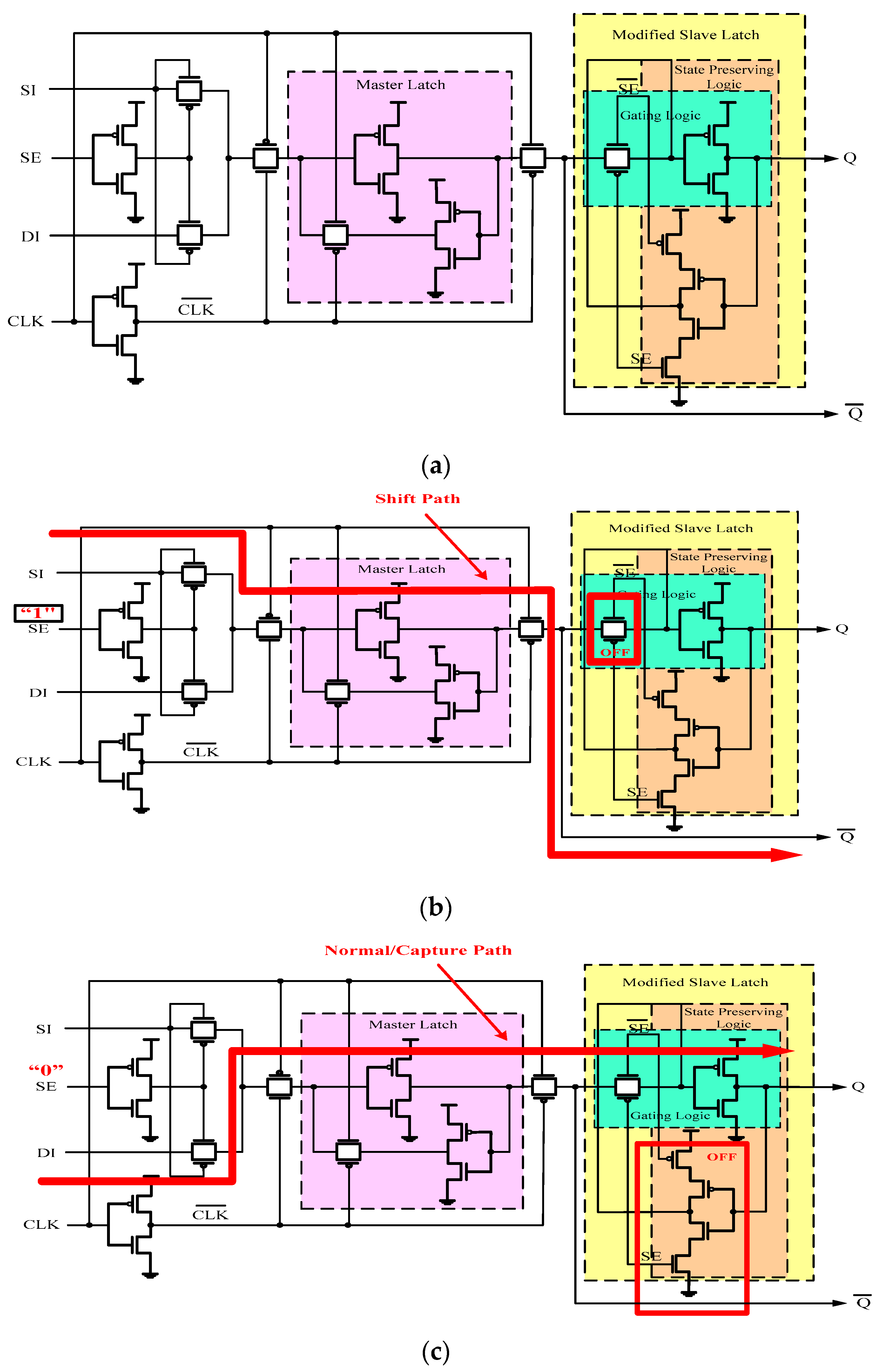
4. Proposed Low Power Gating Scan Cell
During the shift cycle, the rippling transitions cause great switching activities in the scan chain. The propagation of this switching activity into the combinational part contributes to large redundant transitions in the circuit lines. In order to suppress the scan chain transitions from propagating during shift cycles, we have proposed a low power gating scan cell which contains a modified slave latch augmented by a gating logic. For constructing the gating logic, we have utilized a transmission gate and an inverter to gate the scan output to the combinational logic as illustrated in
Figure 2a. It uses the transmission gate to cut off the connection between the inverted scan cell output
and the output
of the scan cells during shift mode. As a result, the switching activities on the
during shift mode does not affect the scan cell output
which is used for driving the combinational logic. High resistance offered by an inactive transmission gate reduces the leakage current in the transmission gate during shift mode and the response capture cycle since the transmission gate is idling in these intervals. In addition, the transmission gate is a strong driver that feeds the gating logic inverter and pseudo primary inputs during normal/capture mode.
Figure 2a–c depicts the proposed low power gating scan cell and the data propagation paths during shift and normal/capture modes of operation, respectively.
In order to totally prevent the unnecessary transitions to the combinational logic during shift mode, a state preserving logic has been proposed. It is a feedback structure that refreshes the scan output
with the previous logic state. The two pull-up and pull-down sleep transistors are active during shift mode which cause the state preserving logic to fix the scan output logic to the same previous logic. However, unlike gating logic, this section is transparent in the normal/capture mode of operation since the sleep transistors are inactive. During this mode, the state preserving logic consumes low leakage power since the two sleep transistors cut off the power rail. The two pull-up and pull-down transistors also contribute to active leakage reduction due to the stacking effect [
44,
45]. These can alleviate the effect of state preserving on peak power during normal/capture mode. The transmission gate, pull-up, and pull-down sleep transistors are driven by the shift enable signal
SE so no extra control signal is required. Sharing the pull-up and pull-down transistors of the state preserving logic among all the scan cells can alleviate the scan chain area overhead.
It is aforementioned that one of the main concerns about gating techniques is the elevated peak power beyond the chip power budget caused by gating logic toggling between gating (shift) mode and transparent (normal/capture) mode. It is noteworthy that the proposed scheme aims to take advantage of the high potential of scan gating approaches in shift power reduction and offers a more practicable scheme by maintaining the scan gating’s average and peak power consumption during capture mode (which are the general side effects of scan gating approaches) as close as possible to that of the conventional scan cell.
It is important to note that, often, capture power consumption refers to transitions that happen within scan cells when they have different values before and after capture. However, in some studies, transitions in the combinational part in launch cycles also have been considered as capture power. In this paper, we consider the whole capture clock cycle including both launch and capture clock edges for evaluating the capture power consumption.
During capture mode, peak power consumption is highly dependent on the test vectors and also test responses that are applied to the scan cell through the functional (DI) input of the scan cell. Moreover, in gating scan cells, the shift enable (SE) signal also has an important influence on the amount of switching activities during capture mode. Hence, the numbers of transitions occuring in the scan cell during capture mode is determined based on two conditions:
Whether the value that is needed to be captured (the value on DI input) is identical to the corresponding test bit value.
Whether the shift enable (SE) signal falls within the capture clock rising edge.
As highlighted earlier, the peak power corresponds to the highest amount of power consumed during a small instant of time tsmall after the application of the test vector. This can be interpreted as the highest number of transistors that simultaneously switch during capture mode. It usually happens at the beginning of each capture cycle due to significant switching activities that occur at the signal lines and transistors due to the circuit mode changing from shift to capture.
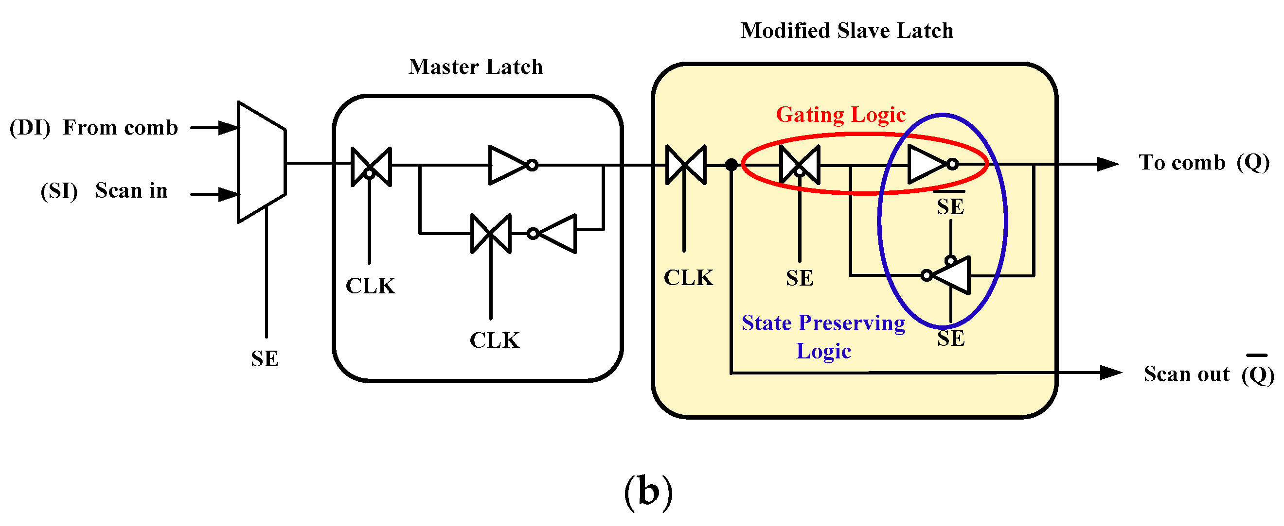
Figure 3a,b demonstrate the gate level implementation of the conventional scan cell and the proposed low power gating scan cell. As seen, the only difference between the architecture of the conventional scan cell and the proposed gating scan cell lies in their slave latch internal structure. Consequently, the difference in the amount of transitions that happen in the modified slave latch of the proposed scan compared with the slave latch of the conventional scan cell can determine the capture power overhead in the proposed gating scan cell scheme.
According to above discussion, in order to present a valid comparison regarding the capture peak power, it is necessary to consider every possible scenario in each scan cell at the beginning of each capture mode.
Here are the possible scenarios that can happen in each scan cell during capture mode.
4.1. Worst Case Capture Switching Activity
In the capture mode of operation, one or both of the following scenarios may happen:
The binary logic of the test response (DI(t+1)) has a different value compared with the corresponding test vector bit on the Q output of the scan cell (SI(t)).
Test pattern pairs (V1,V2) are applied to the circuit-under-test (CUT) through scan cells in launch-off-capture (LOC) transition fault testing. Pattern V1 and pattern V2 include non-identical corresponding pattern bits to propagate the transition and capture it at an observation point.
4.1.1. Conventional Scan Cell
It causes both feedback inverters in the conventional slave latch to switch. In addition, there are two transmission gates in the conventional slave latch controlled by the clock that contribute to capture switching as the capture clock rises. Therefore, the total numbers of switching transistors in the conventional slave latch is eight (8) transistors.
4.1.2. Proposed Low Power Scan Cell
In this case, the number of switching transistors in the modified slave latch vary depending on the time that the shift enable (SE) signal toggles from “1” to “0”:
The shift enable (SE) signal falls simultaneously with the capture rising clock, and then the total number of switching transistors in the modified slave latch will be six (6) transistors, including two transmission gates and two feedback inverters. Note that the inverter in the refresh feedback does not contribute in switching activity as the two sleep transistors disconnect it from the power supply and ground during the capture mode of operation.
The shift enable (SE) signal falls before the capture rising clock, and then the total number of switching transistors in the modified slave latch will be four (4) transistors, including the transmission gate that is controlled by the clock and inverter in the scan cell functional path. Note that since the shift enable signal has already switched from “1” to “0” earlier, the inverter in the refresh feedback as well as the transmission gate controlled by the shift enable (SE) signal likely do not contribute in toggling in this capture scenario, as the former is disconnected from the power supply and the latter merely behaves as a connected switch.
Considering the worst case scenario for the conventional scan cell and both possible worst case scenarios for the proposed gating scan cell, it can be seen that the proposed scan cell is able to reduce the peak power compared to the conventional scan cell. This is because the proposed low power gating scan cell compared with the conventional scan cell causes less number of transistors to switch simultaneously inside the scan cell during the application of test vectors (capture mode). To the best of our knowledge, there is no gating scan cell found in the literature that is able to reduce the capture peak power over the conventional scan cell.
The proposed low power gating scan cell works as a flip-flop because the inserted state preserving logic together with the gating logic function as a modified slave latch which has power reduction roles. Due to the shift path with less complexity, the scan cell speed has been accelerated during shifting which consequently alleviate the setup time violations. However, like other scan cells, the hold time violation concerns still exist. The reduced area and propagation delay due to the removal of two inverters and a transmission gate in the scan structure can moderate the area and delay overhead imposed by the augmented gating logic and also the state preserving logic.
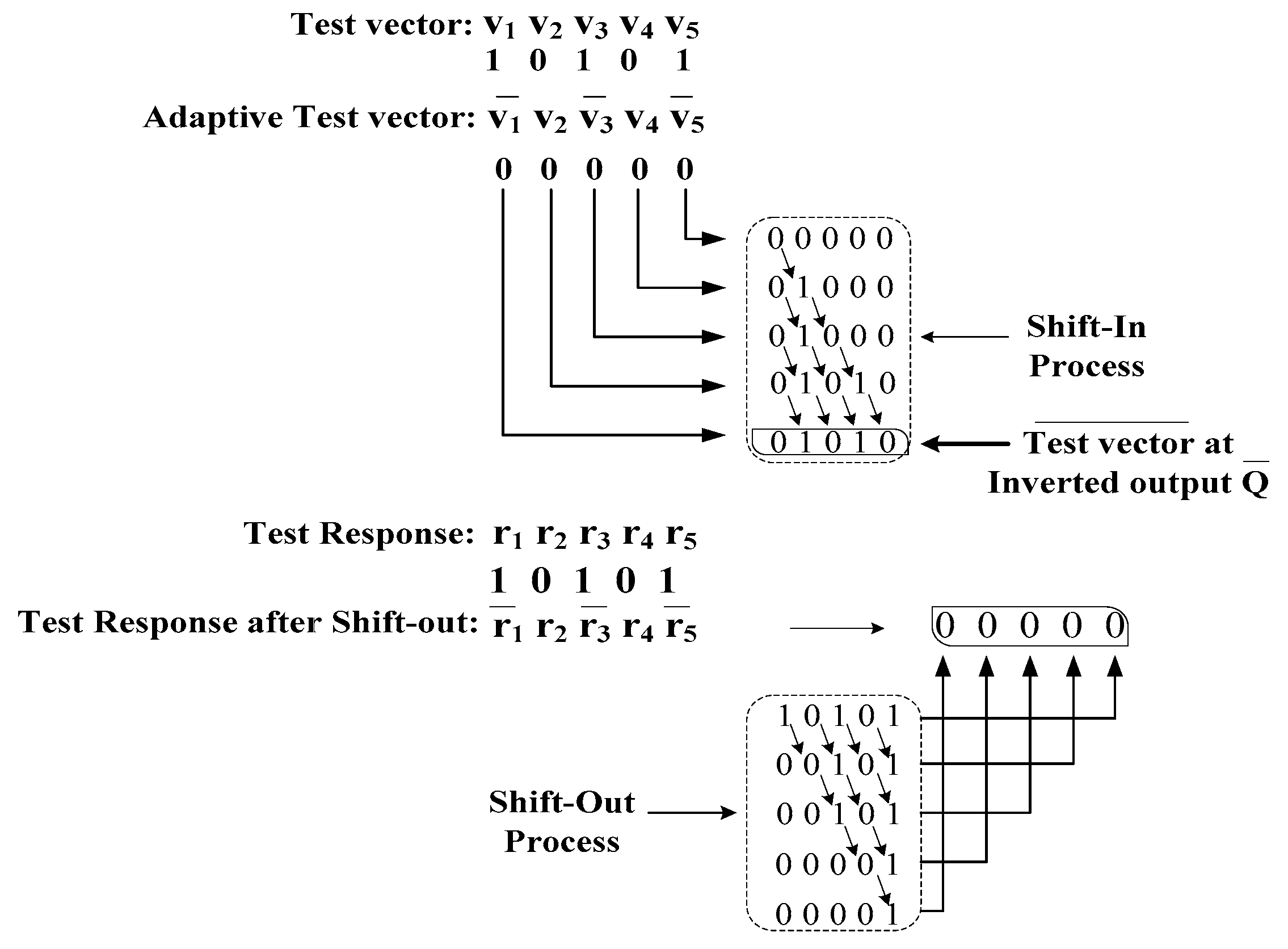
Since the shift path in the proposed scan cell has been established through the
output of scan cell, adaptive test patterns can be used instead of original ones. The adaptive scan process has been summarized in
Figure 4.
Let
vi represent a test pattern to be shifted to a scan cell. The adaptive test patterns are generated such that
is shifted to the destination of the inverted scan cell after the shift-in process.
is inverted to
vi after going through gating logic during the test application. Let
be an adaptive test pattern and 1 ≤
i ≤
N where
N is the number of scan cells in a scan chain.
vi for an even index
i and
for an odd index
i whether
N is an odd or even number. The adaptive test pattern formulation is as follows.
Modifications are necessary for test responses after the shift-out process since the responses are captured by the inverted scan cells. Let ri represent the test response of a pseudo output. After being captured by the inverted scan cell, it becomes The shifting process of takes place along the inverted scan cells. Let be the test response that reaches scan-out after shifting where 1 ≤ i ≤ N and N is the number of scan cells. for an odd index i and for an even index i when N is an odd number, while for an odd index i and for an even index i when N is an even number. The modifying test pattern formulation is as follows.
For
N number of scan cells when
N is an odd number:
For N number of scan cells when
N is an even number:
Therefore, an inversion needs to be performed on when to retrieve the correct test response for the response comparison.
It is noteworthy that the mentioned adaptive scan process is fully automated and will be carried out with the automatic test pattern generation (ATPG) tool. Since the adaptive test vector and the expected test response after shift-out is generated by the ATPG tool after scan insertion of the synthesized circuit using the proposed scan structure, the proposed structure does not have any impact on the original fault coverage.
5. Experimental Results and Comparisons
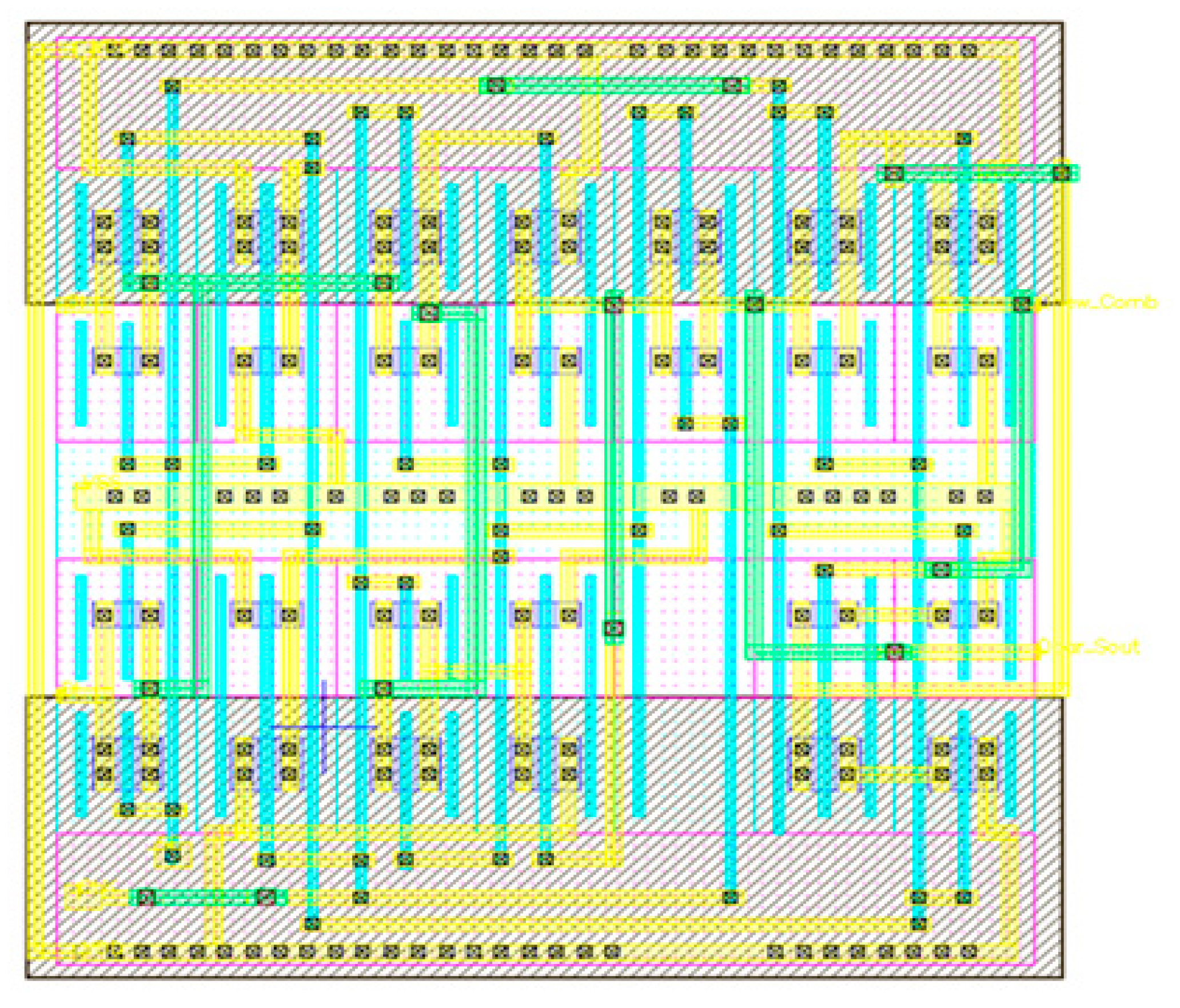
The proposed low power gating scan cell has been implemented through conducting a full-custom layout design incorporating the Synopsys Custom Designer and Laker.
Figure 5 shows the full-custom layout design for the proposed gating scan cell. Next, in order to verify the proposed scan cell, a set of post-layout simulations has been carried out on the parasitic included spice netlist using HSPICE in Synopsys 32/28 nm CMOS technology with the supply voltage of 1.05 Volt and clock frequency 250 MHz at room temperature. The simulation results were then compared to the conventional scan cell and the modified scan cell presented in [
34] in terms of power, propagation delay, power-delay-product (PDP), and area overhead. The power consumption and propagation delay were observed by applying randomly generated waveforms.
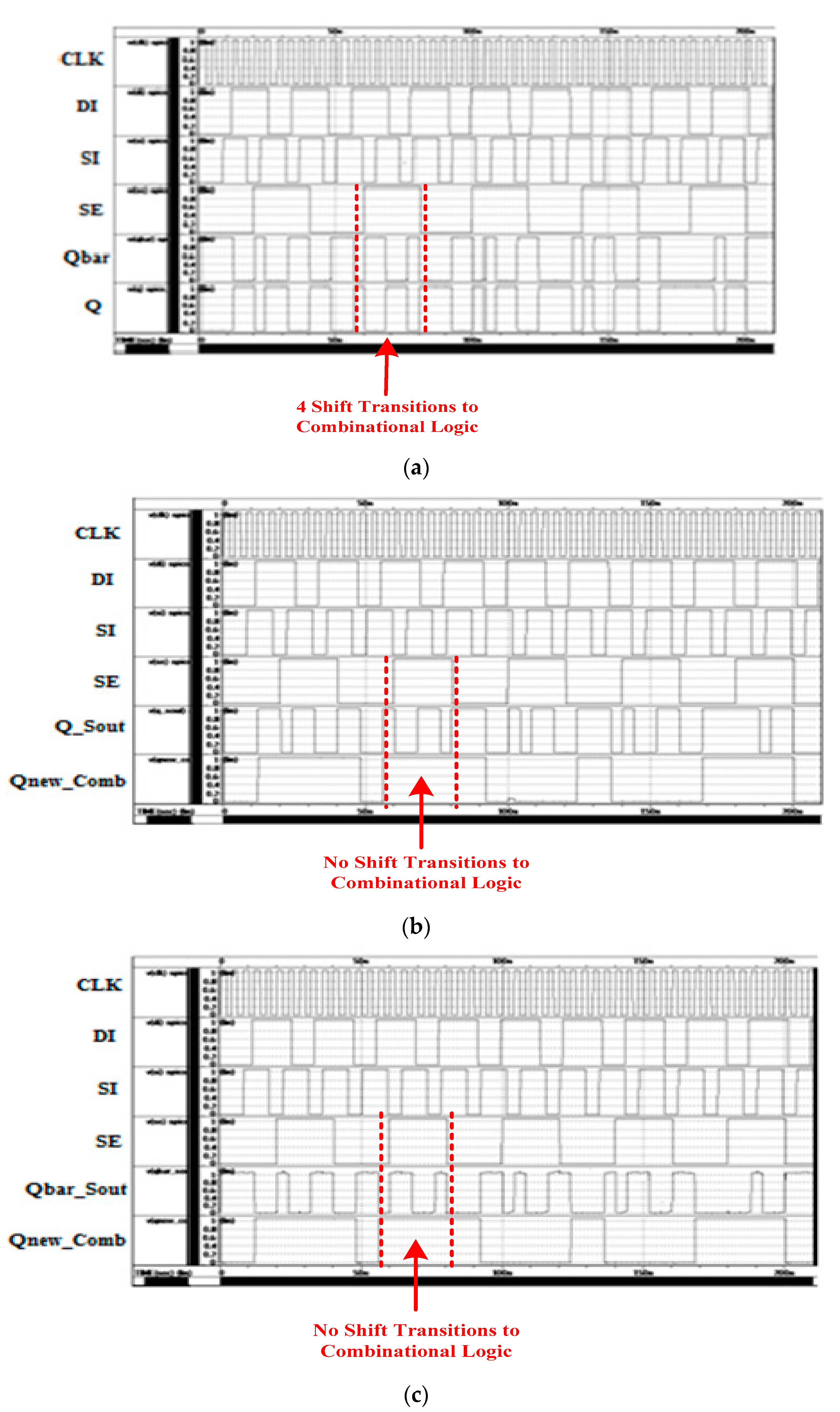
The simulated output waveform of each scan cell to the combinational logic has been shown for the conventional scan cell, proposed gating scan cell, and modified scan cell in
Figure 6. It is clearly seen that unlike the conventional scan cell, the proposed gating scan cell and the modified scan cell have no transitions in the combinational logic during the shift session, as the scan cell output “
Qnew_Comb” remains the same while the shift enable (
SE) is high. Note that, “
Qnew_Comb” is the scan cell output connecting to the combinational part.
In order to clarify the transition reduction ratio (TRR) at the functional output of each scan cell, we have pointed out one sample shift cycle with red dotted lines in the post-layout simulated waveforms for the conventional scan cell, proposed scan cell, and modified scan cell presented in [
34] (see
Figure 6). It is clearly observable that the proposed scan cell and modified scan cell are both able to totally suppress the transitions on the functional path of the scan cell and consequently combinational logic during shift mode. This means a 100% Transition Reduction Ratio (TRR) on the scan cell functional path is achievable during shift mode using the state preserving hold technique employed in the proposed gating scan cell as well as the modified scan cell. Moreover, the number of transitions on the “
Qnew_Comb” (which is the proposed scan cell output connecting to the combinational part) during the whole test application time has been reduced from 26 transitions to 8 transitions in the proposed gating scan cell and the modified scan cell for the identical applied test patterns. This means a 69.93% Transition Reduction Ratio (TRR) during the whole test application has been achieved using the state preserving hold technique.
The main goal to be achieved by the proposed low power gating scan cell is to reduce the power consumption not only in the combinational part but also inside the scan cell structure as well. This makes the proposed low power gating scan cell more distinct compared to the modified scan cell and existing scan gating approaches. In the next part, a comparative analysis study of the power consumption for one scan cell has been reported in terms of the scan cell total average power during the whole test application time, shift power, and capture power. The latter refers to peak power since the logic values in many scan cells change simultaneously during this mode.
5.1. Post-Layout Scan Cell Simulation Results
The comparative analysis results on total power consumption for each scan cell are shown in
Table 1. To evaluate the total power consumption, identical random patterns are applied to each scan cell and the total power consumption during both test and normal modes of operation is observed. As shown in
Table 1, the proposed low power gating scan cell achieves a 7.21% improvement on average in terms of the total power consumption inside the scan cell over the conventional scan cell. The negative 26.97% improvement obtained for the modified scan cell implies that unlike the proposed gating scan cell, this scan cell increases power consumption over the conventional scan cell. Thus, it is only able to reduce power dissipation in the combinational part, during shifting.
Table 2 shows the improvement of power consumption for our proposed scan cell and the modified scan cell over the conventional scan cell in four successive shift cycles. The proposed scan cell outperforms both the conventional scan cell and modified scan cell in all shift cycles. This is because it exploits a shorter shift path with less complexity compared to the other mentioned scan cells.
In order to show the impact of the proposed gating scan cell on the peak power, we have compared the percentage of peak power increase in the proposed gating scan cell and modified scan cell over the conventional scan cell through four successive normal/capture cycles (each including one clock period).
Table 3 backs up our earlier claim regarding the capture peak power reduction in the proposed scan cell over the conventional scan cell since the modified slave latch in the proposed scan cell is able to reduce simultaneous transistor transitions at the beginning of the capture cycle. It shows the peak power consumption during four capture cycles for the proposed gating scan cell and modified scan cell over the conventional scan cell. It can be seen that the proposed scan cell is able to improve peak power over the conventional scan cell during all capture/normal cycles up to 5.32%, while the modified scan cell increases peak power in all investigated normal/capture cycles (up to 19.10% in second capture cycle).
In
Table 4, various delay arcs for all compared scan cells has been reported in two sub-sections. The first sub-section represents the exact amount of propagation delay for each scan cell and the achieved percentage of improvement in each (shift, capture, and launch) path over the conventional scan cell. It is observable that the proposed gating scan cell delivers improvements on shift delay and capture delay over the conventional scan cell by 3.08% and 1.12%, respectively.
It can be noticed that, the achieved improvement in shift delay is on the scan cell level. However, the improvement in shift speed in large industrial designs highly depends on the number of scan cells in the scan chain due to the serial nature of shifting. Our proposed gating scan cell causes delay overhead on the scan cell data path to combinational logic by 2.82% through the normal/capture mode of operation.
The calculated propagation delay on the clock signal in shift (CLK-to-shift output) and launch (CLK-to-launch-output) has been presented as the percentage of simulated clock period in the second sub-section. According to this sub-section, the portion of time is needed to be taken for propagating data through the shift path after the rising edge of the clock for the proposed scan cell is 0.61% of the clock period that corresponds to 50.7% and 37.86% improvements in the CLK-to-shift output over the conventional scan cell and modified scan cell, respectively. Finally, the last row in
Table 4 refers to exact amount of PDP for each related scan cell. It is interesting to note that although the modified scan cell delivers better propagation delay on the clock to launch output, the proposed scan cell still outperforms the modified scan cell in terms of PDP.
It is noteworthy that the increased complexity in the proposed scan cell regarding the delay overhead on the data launch path and also the launch clock in the proposed gating scan cell may raise the question of violating the timing closure on critical paths. Note that we implemented sleep transistors in state preserving with a minimum transistor size in 32/28 nm CMOS technology. However, a further improvement in launch delay can be achieved by up-sizing the sleep transistors referred to in [
33]. This does not have any effect on the gate switching activity and it only has a penalty in terms of the area. Furthermore, partial gating techniques can be practiced by identifying those scan cells which can meet the timing closure after getting substituted by the proposed gating scan cell. This will result in power reduction in both the scan chain and combinational part at no performance degradation cost.
To evaluate the area overhead imposed by the proposed structure, we calculated the actual size of the proposed gating scan cell from the layout design. The routing overhead has not been considered in the area overhead. However, the routing overhead associated with the proposed gating structure should not be high since no additional control signal is required. In the same manner, the area overhead for the conventional scan cell and modified scan cell has been measured. The largest ITC’99 benchmark circuits were chosen in order to show the impact of the proposed scan cell on the circuit area overhead. Furthermore, the full gating architecture has been considered for all benchmark circuits as an index for the worst case of the area penalty. We have considered the actual scan chain size in each benchmark circuit as a metric for calculating the area overhead in each case. Since the compared scan cells address the area overhead only on the scan chain structure, they do not have any impact on increasing the combinational part area.
Table 5 shows the characteristic of the selected benchmark circuits.
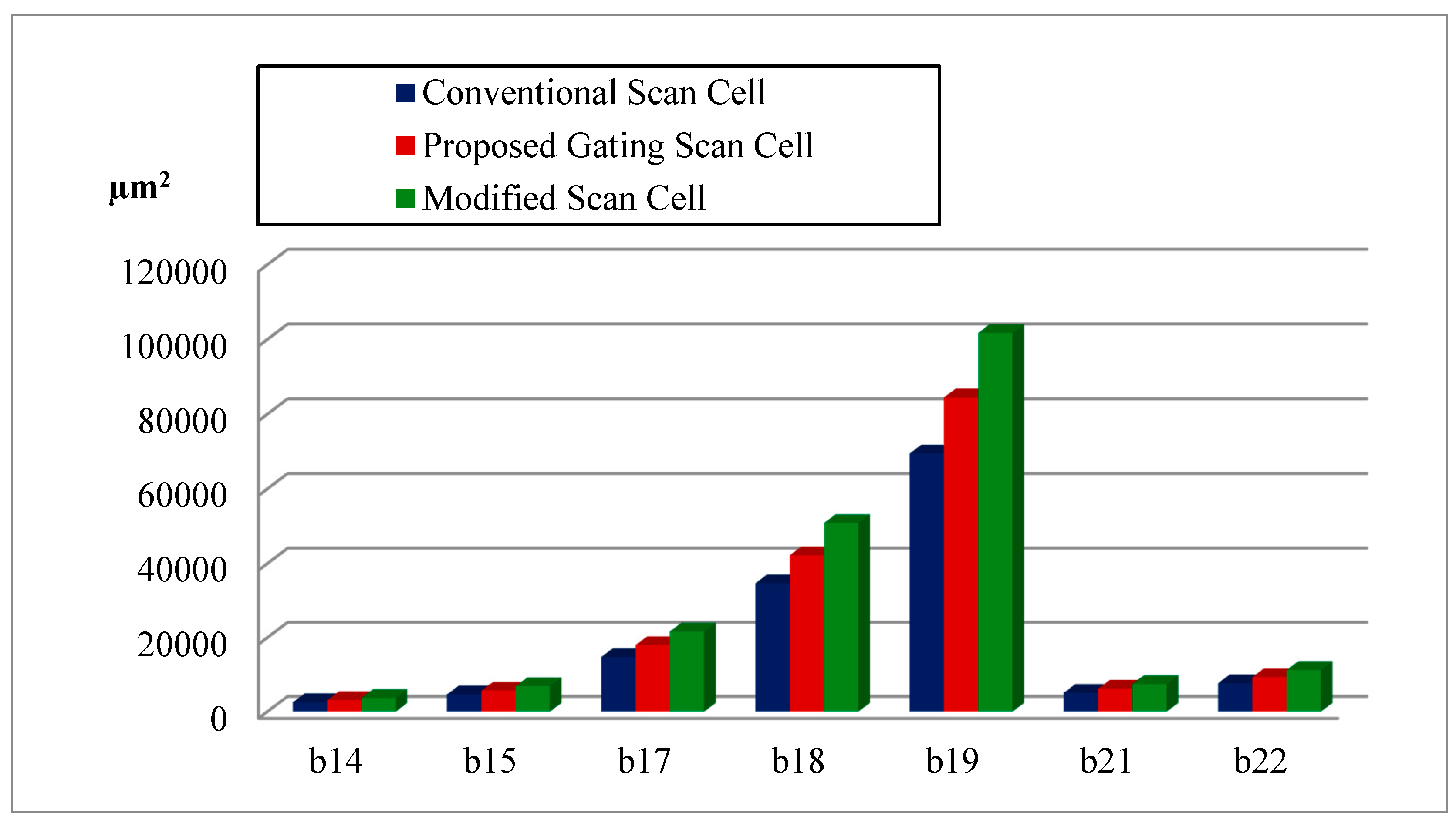
In
Figure 7 the actual size of the scan chain for each compared scan cell has been shown. It is observable that the area overhead addressed by the scan chain has been reduced in the case of using the proposed scan cell compared with the modified scan cell by 20.4%. The achieved improvement for the proposed scan cell in the area overhead remains at the same level for all benchmark circuits regardless of the circuit size.
In order to alleviate the active area taken up by the proposed gating scan cell, the pull-up/down sleep transistors in state preserving logic can be shared between all scan cells in the full gating architecture. In partial gating architecture, only those scan cells that are on non-critical paths share the sleep transistors. We have considered the full gating scan in our experiment and have assumed that for random input patterns, nearly half of the scan cells do not switch and the pull-up and pull-down transistors are exercised for almost half of the scan cells at the same time. Thereby, the channel width for shared pull-up and pull-down transistors are chosen as follows.
where
FF is the number of scan cells. The active area for the shared pull-up and pull-down transistor is calculated based on the total transistor active area (
W × L for a transistor) and is denoted by AreaPull-up and AreaPull-down, respectively.
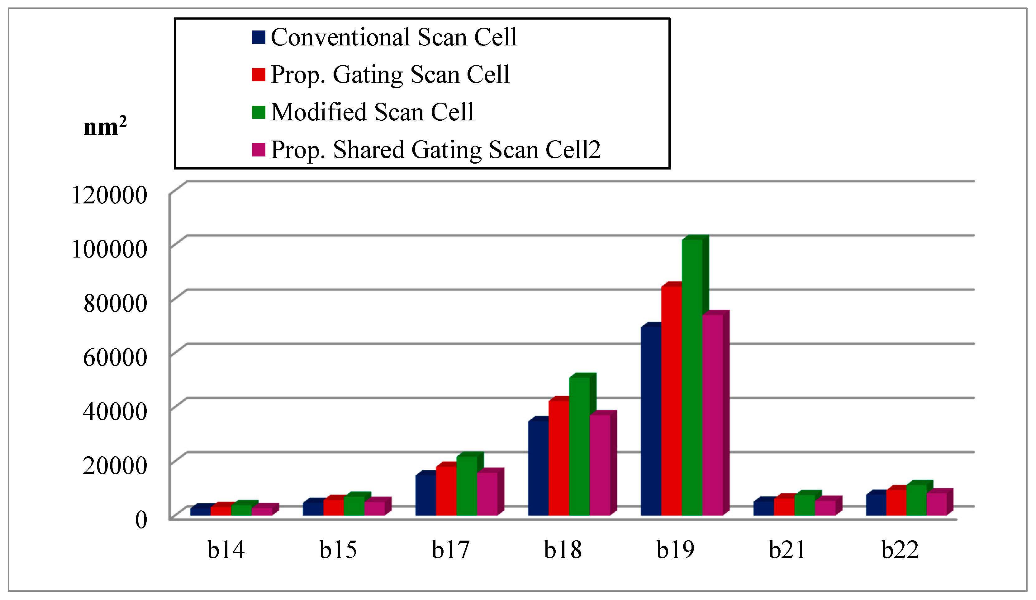
Next, similar to previous experiments, the actual size of the proposed design excluding the pull-up and pull-down sleep transistors has been extracted from the layout design. Based on this discussion, the actual size of benchmark circuits fully gated by the proposed low power gating scan cell is given by
Figure 8 indicates the area overhead of the proposed shared low power gating scan chain for the different benchmarks compared with the conventional scan chain and modified scan chain. As can be seen, improvement in area overhead has been achieved by 12.46% for the proposed shared low power gating scan chain compared with the proposed low power gating scan chain. The observed area overhead penalty for the shared low power gating scan chain compared with the conventional scan chain is 6.45% for all benchmark circuits.
5.2. Vector-Dependent Power Analysis Results
In the previous section, the simulation results and discussions were presented for each scan cell. This section provides simulation results on the shift and capture power consumption for several ITC’99 benchmark circuits. In this experiment, each benchmark circuit first was scan inserted with the conventional scan cell and next with the proposed low power gating scan cell. The results on the shift and capture power are then compared for power improvement calculations.
Power consumption evaluations for benchmark circuits were carried out by synthesizing and scan insertion of the ITC’99 benchmark circuits in the Synopsys Design Compiler. The test patterns for transition fault models were then generated for the gate-level mapped netlists using Synopsys TetraMax in 32/28 nm standard CMOS technology for all possible corners, including the worst case corner of the fast NMOS and fast PMOS transistors. Next, the Verilog test-benches generated by Synopsys TetraMax for each benchmark circuit were dumped into VCD files using Synopsys VCS. The VCD files were then used by Synopsys PrimeTime PX to create the vector-dependent power reports during the shift mode and capture mode.
Table 6 shows the percentage of shift power improvements for each benchmark circuit using the proposed low power gating scan cell over the conventional scan cell to form their scan chain.
As it is stated in
Table 6, all simulated benchmark circuits employing the proposed low power gating scan cell showed significant improvements up to 67.4% and 84.8% in shift dynamic and peak power, respectively.
Table 7 represents the percentage of capture (average and peak) power improvements for each benchmark circuit utilizing the proposed low power gating scan cell over the conventional scan cell in their scan chain. It is clearly observable that all simulated benchmark circuits achieve considerable capture peak power improvement up to 80.2%. As shown earlier in
Table 1, one proposed scan cell is able to improve the capture peak power over one conventional scan cell in the worst case scenario. Consequently, significant peak power reductions have been observed in benchmark circuits composed of hundreds or thousands of scan cells.
However, all benchmark circuits using the proposed low power gating scan cell show a capture average power penalty up to 11.8%. This is because unlike peak power that is defined based on the highest instantaneous power, capture average power is determined based on the internal power, switching power, leakage power, and net switching power over a period of time. The proposed low power gating scan cell implements gating logic in the modified slave latch by an extra transmission gate (controlled by shift enable (SE) signal) compared with the conventional scan cell, and therefore results in higher capture average power.
It is noteworthy that, similar to the existing scan gating approaches, the proposed low power scan cell aims for shift power reduction through suppressing the redundant transitions from the scan cell to combinational logic during shift mode. As mentioned earlier, current scan gating techniques increase capture (average and peak) power as a result of the redundant switching activity occurring in gating logics. However, one of the main advantages of the proposed scan gating scheme is that contrary to the existing scan gating techniques, it is able to maintain the capture average power close to that in the conventional scan cell and even improve the capture peak power over the conventional scan cell by implementing internal gating logic in the scan cell’s slave latch. In other words, the proposed scan cell does not reduce capture power compared to the conventional scan cell, however unlike current scan gating techniques, it does not cause a high elevation in capture power.
Hence, power-aware ATPG techniques can be utilized as an alternative solution in conjunction with the proposed gating scheme in order to reduce the excessive power consumption during capture mode.
7. Conclusions
One of the less intrusive and effective solutions to reduce shift power significantly, independent of the test set, is scan gating techniques. However, significant delay on signal propagation paths, large area overhead, high switching activity, and finally undesired impacts on peak power all caused by gating logics, has made them less practical for large industrial circuits. Most previous works successfully reduce shift power in combinational logic only, without considering the scan chain as the main source of power consumption during the shifting phase. In this paper, we designed and implemented an area-efficient low power gating scan cell as an integrated solution for shift power reduction in both the scan chain and combinational logic. Since the gating scan cell reduces power consumption inside the scan cell compared with the conventional scan cell, the total power consumption is reduced during the shift (test) mode of operation. The proposed gating scan cell is a modified scan cell augmented by gating and state preserving logics to gate and hold the scan cells' stimulus path while maintaining peak power under a certain threshold. Choosing a new data shift path through a less complex propagation path in the proposed gating scan cell incorporates further power reduction in the scan chain in addition to improving the critical shift timing and hence, leads to test application time reduction. Compared with the lowest cost gating techniques, the proposed gating scan cell has less DFT overhead with respect to average power, shift, and capture delay. Similar to other gating methods with state hold abilities such as the modified scan cell, the proposed low power gating architecture can be effectively employed in broadside delay fault test applications. Furthermore, it can be applied effectively to both the full gating and partial gating methods. The original fault coverage is not degraded and it does not face routing problems since no additional control signal has been employed. The proposed scheme can efficiently be utilized in both built-in-self-test (BIST) and non-BIST architectures. It can also be applied together with other scan-based power optimization methods such as scan chain partitioning and reordering techniques. Low power hardware-based as well as ATPG-based methods can be applied to the proposed structure efficiently for capture average power reduction. Therefore, these advantages make the proposed approach a potential candidate for all scan-based DFT architectures.


