Article

Ultra-Low Power, Process-Tolerant 10T (PT10T) SRAM with Improved Read/Write Ability for Internet of Things (IoT) Applications

by
Pooran Singh
* and
Santosh Kumar Vishvakarma
Indian Institute of Technology Indore, Simrol, Indore 453552, India
*
Author to whom correspondence should be addressed.
J. Low Power Electron. Appl. 2017, 7(3), 24; https://0-doi-org.brum.beds.ac.uk/10.3390/jlpea7030024
Submission received: 2 August 2017 / Revised: 5 September 2017 / Accepted: 13 September 2017 / Published: 20 September 2017

Abstract

:
In this paper, an ultra-low power (ULP) 10T static random access memory (SRAM) is presented for Internet of Things (IoT) applications, which operates at sub-threshold voltage. The proposed SRAM has the tendency to operate at low supply voltages with high static and dynamic noise margins. The IoT application requires battery-enabled low leakage memory architecture in a subthreshold regime. Therefore, to improve leakage power consumption and provide better cell stability, a power-gated robust 10T SRAM is presented in this paper. The proposed cell uses a power-gated p-MOS transistor to reduce the leakage power or static power in standby mode. Moreover, due to the stacking of n-MOS transistors in 10T SRAM latch and by separating the read path from the 10T SRAM latch, the static and dynamic noise margins in read and write operations has shown significant tolerance w.r.t. the variations in device process, voltage, and temperature (PVT) values. The proposed SRAM shows significantly improved performance in terms of leakage power, read static noise margin (RSNM), write static noise margin (WSNM), write ability or write trip point (WTP), read–write energy, and dynamic read margin (DRM). Furthermore, these parameters of the proposed cell are observed at 8-Kilo bit (Kb) SRAM and compared with existing SRAM architectures. From the Monte Carlo simulation results, it is observed that the leakage power of a proposed low threshold voltage-LVT 10T SRAM is reduced by 98.76%, 98.6%, 6.7%, and 98.2% as compared to the LVT C6T, RD8T, LP9T, and ST10T SRAM, respectively, at 0.3V VDD. Additionally, in the proposed 10T SRAM, parameters such as RSNM, WSNM, WTP, and DRM are improved by 3×, 2×, 1.11×, and 1.32×, respectively, as compared to C6T SRAM. Similarly, the proposed 10T SRAM shows an improvement of 1.48×, 1.25×, and 1.1× in RSNM, WSNM, and WTP, respectively, in the parameters as compared to RD8T SRAM at 0.3 V VDD.

1. Introduction

The constraint of high standby power present in Internet of Things (IoT) devices has encouraged the developments of ultra-low power subthreshold SRAM architectures [1,2]. Scaling down the supply voltage is the best way to improve the total power consumption [3]. However, this results in reduction of on-to-off current ratio (ION/IOFF). This will further affect the read offset voltage required for sensing the bit information stored in SRAM cell. Moreover, in the sub-threshold region, the drain current, which exponentially depends upon the threshold voltage (Vth), introduces numerous challenges such as high standby power, low read and hold stability and read failure. Nevertheless, the low read and write stability are also major factors that resist conventional SRAM architectures to work in the sub-threshold region [4]. Due to the rapid growth of the Internet market, the IoT brings connectivity, communication, and data gathering to existing devices. The IoT allows countless devices to be connected and communicating with each other to enrich the present lifestyle. Applications of IoT range widely from traditional Internet and industrial Internet to consumer Internet [5].
The SoC block of IoT contains various sub-systems like sensors, communication ports, security blocks, high-end processor, and on-chip memories, which consist of read-only memory (ROM) and static random access memory (SRAM). However, SRAM has been divided into two types of systems, namely fast and low power, each of with has its own advantages, features, and applications. The IoT devices where SRAMs are used as memory storage needed it for either its high speed or low power consumption depending upon its application. Nevertheless, there is high demand for high-performance devices with ultra-low power consumption to execute composite operations while running on portable devices. This demand is mostly driven by new-generation medical devices, handheld devices, and communication systems that are fulfilled by the IoT devices. The development of the IoT is headed in two distinctive directions, i.e., smart wearables and automation. The wearable devices uses SRAM as a memory element that has a small footprint and low power consumption. Thus, SRAMs with high speed, high stability, and low power consumption are of significant importance to IoT devices and its applications.
Moreover, the IoT portable devices communicate with each other and thus require an enormous amount of memory to store and process data. The memory requirement in IoT depends upon the applications related to the market. For instance, in the case of a huge amount of data storage and handling information for a long period of time, high-density memory like DRAM and Flash are required. On the other hand, for high data transfer rate systems, fast SRAM memory is required, where a high speed data transfer is essential to communicate between IoT devices. Therefore, SRAM is preferred as a cache memory due to its faster response. Moreover, the robustness of such memory systems with respect to the variations in process–voltage–temperature (PVT) values of metal oxide semiconductor devices (MOS) and power efficiency are two of the most important design constraints [4]. As per the literature, more than 40% of the active energy is consumed due to the leakage current in modern high-performance processors [6,7]. Moreover, most of the time a large number of the SRAM cells used in present-generation on-chip cache memory are in a holding state where leakage power dominates over the dynamic power. Thus, leakage reduction has become an imperative concern in SRAM memory design.
To overcome the issue of leakage of power in subthreshold SRAM due to variations in various process parameters like channel length, gate-oxide, DIBL, etc. and the unpredictability in device performance and instability due to noise generated from high bitline static voltage and thermal noise generated from temperature variations, a differential process-tolerant 10T SRAM cell is proposed in this paper. The rest of the paper is organized as follows: related work and motivation are detailed in Section 2. A proposed 10T SRAM architecture with 64 × 128 array (8-Kb) is presented in Section 3 and Section 4, respectively. The operations and working of 8-Kb SRAM are explained in Section 5. The simulation results and a discussion of proposed 10T SRAM are given in Section 6. Section 7 is a summary of results. Lastly, Section 8 concludes the work.

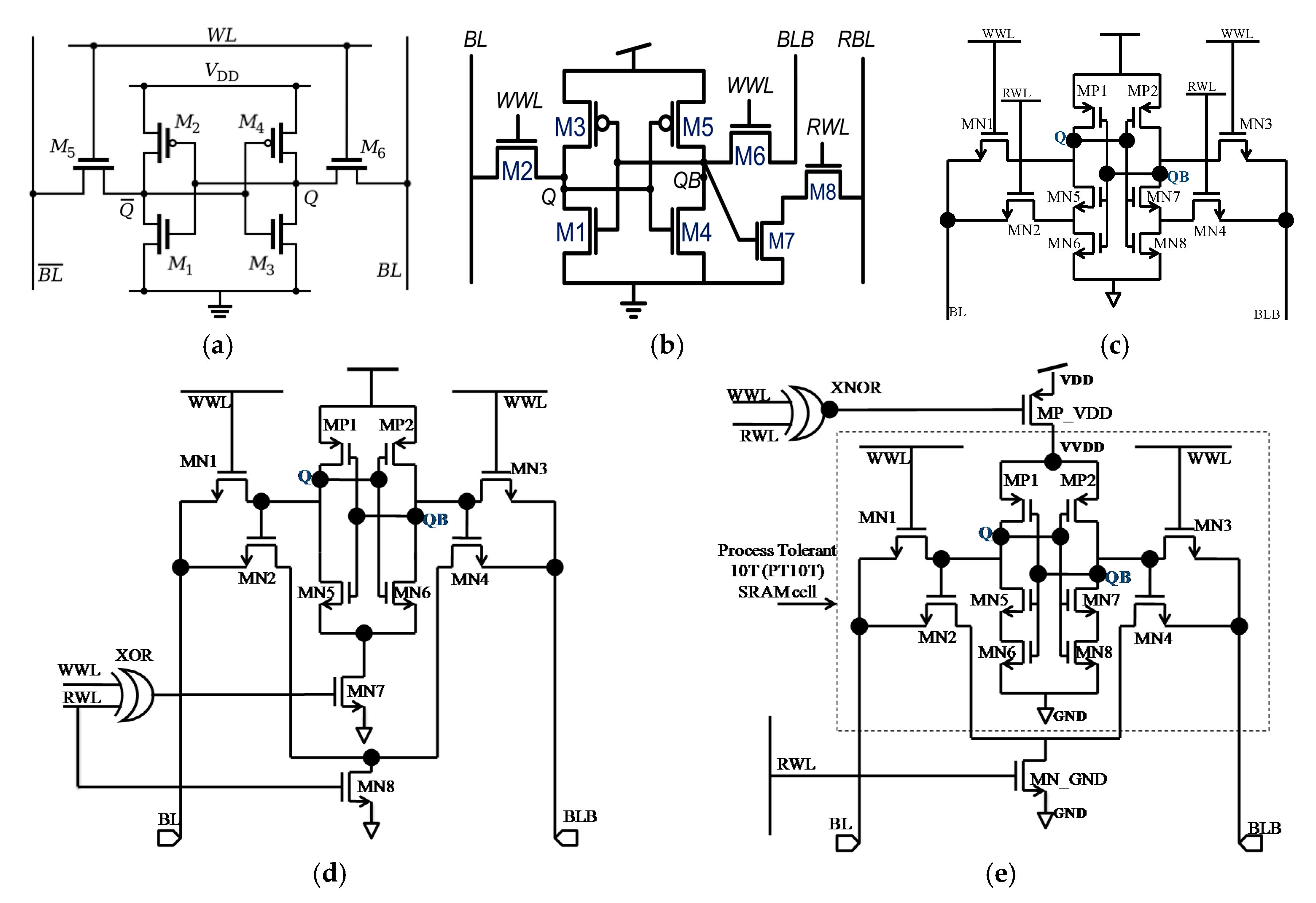
2. Related Work and Motivation

It is observed that leakage power and cell stability are the key concerns in subthreshold SRAM architectures to improve the reliability, yield, and susceptibility of portable electronic devices. Moreover, SRAM cells are in a static or holding state most of the time, which contributes to the high leakage. Furthermore, cell stability is also a foremost concern in the subthreshold region. The noise generated from threshold variation, process variation, half-select issue, and multiple bit errors reduces the stability of SRAM cell. Consequently, various techniques have been developed to overcome the noise generated from these constraints, such as scaling the supply voltage using process-variation-tolerant Schmitt trigger-based ST10T SRAM [8], a read static noise margin-free 7T SRAM [9], differential data aware power-supplied D2AP8T SRAM [10], low-leakage, variation-tolerant LP8T [11], LP9T [12], and LP10T SRAM [13]. Besides the advantages observed from these SRAM architectures, there are some drawbacks like larger area, high cost, low WTP, low WSNM, and higher energy requirement in a subthreshold region. To compensate for all these factors, along with low leakage power and better cell stability, a differential ultra-low power, process-tolerant 10T SRAM is proposed in this paper. The conventional 6T SRAM shown in Figure 1a has a tendency to fail in subthreshold voltages due to the read path sharing of the M5 and M1. However, to improve RSNM, an 8T SRAM shown in Figure 1b is proposed that reads information through a decoupled read path. In a decoupled read the read access time increases. To improve reading speed with better RSNM, a Schmitt triggered 10T (ST10T), shown in Figure 1c, is presented [8]. However, in ST10T the charge sharing still exists in read and write, which eventually degrades the read/write static noise margin and write ability. To overcome the problem related to read delay and static noise margin, a low-leakage 10T (LP10T) SRAM is presented in [13], as shown in Figure 1d, which improves the leakage power by introducing a virtual ground path and noise margins by differential decoupled read. However, the stack transistor MN8 used in [13] at the ground pushes the storage node to meta-stability. The meta-stability is not considered a good choice to exist in subthreshold supply voltages, where a small gain in storage node voltage flips the state of the cell. However, to overcome the state of meta-stability and improve the leakage power generated in subthreshold operation in a proposed 10T (shown in Figure 1e), a power gated p-MOS is used. In addition, to improve read and write static noise margin, a separate read path and stacked n-MOS structure is used in proposed 10T SRAM latch. The stacking of MN5-MN6 and MN7-MN8 results in a higher write trip point and WSNM. However, by separating the read path (BL-MN2-MN_GND) from the latch and creating a complete isolation of storage nodes from BLs, the RSNM of proposed 10T SRAM is improved as compared to C6T, RD8T, and ST10T. However, improving these parameters contributes to more area and eventually to a higher cost of SRAM. Furthermore, the SRAM cell and macroblock architecture with area overhead are further detailed in Section 3 and Section 4, respectively.

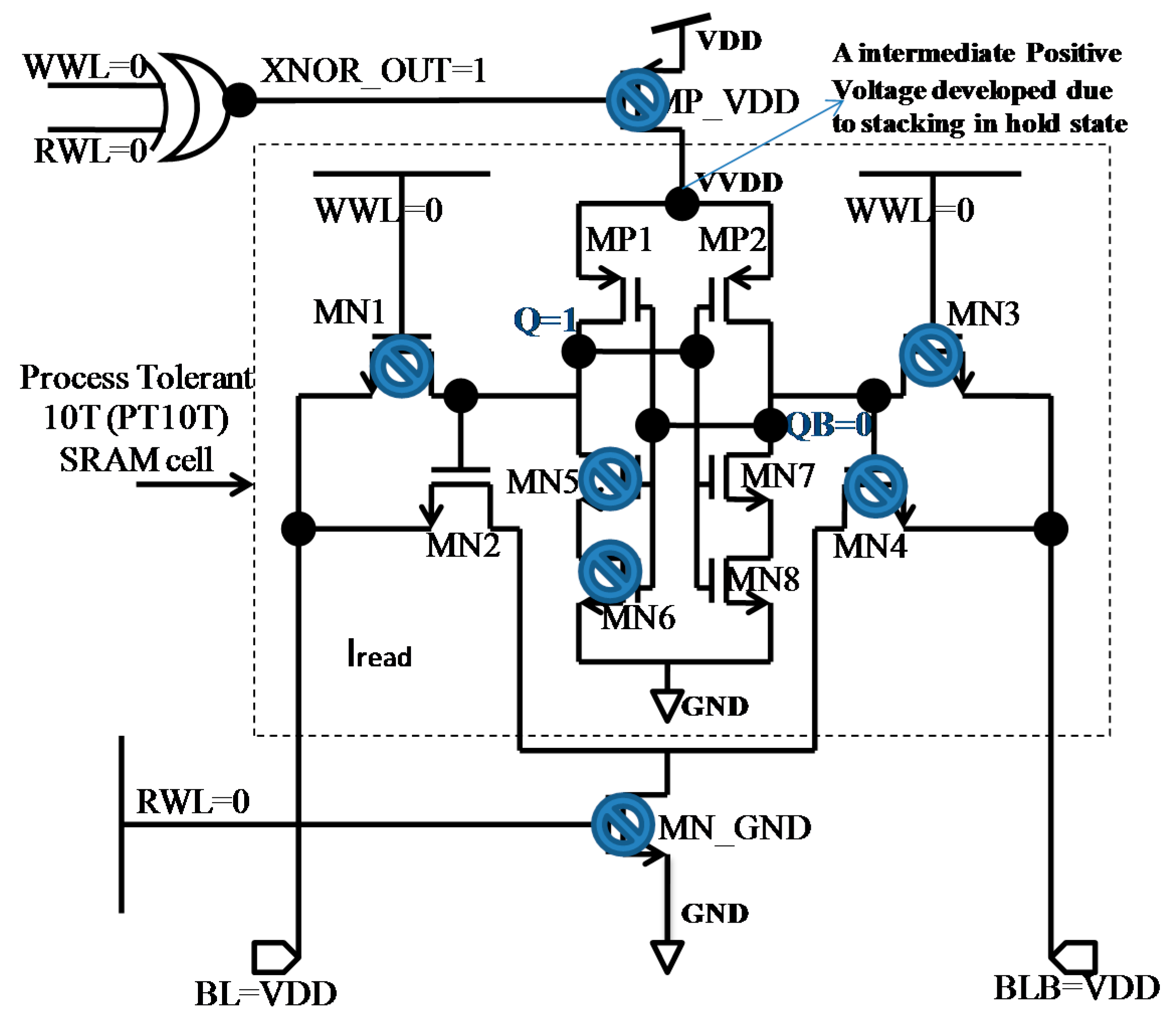
3. Architecture of 10T SRAM Cell

The advancement in technology and reduction in IC development cost due to smaller die area resulted in considerable improvement in digital electronic devices. If this development continues, it will result in a world where all the digital electronic devices linked to the Internet, known as the Internet of Things (IoT). Furthermore, a millions of zettabytes of memory is required to handle the large-scale computations required by IoT devices. Thus, memory plays a vital role in future energy-efficient computing systems and, therefore, a subthreshold, low-leakage and high-stability SRAM is proposed in this section.
The proposed cell shown in Figure 1e has two-write access n-MOS transistors, MN1 and MN3, and two read-access transistors, MN2 and MN4. BL contains single-bit information to write; BLB contains the complementary of that. Furthermore, the cell layout structure of proposed cell along with the existing SRAM cell is shown in Figure 2. In addition, n-MOS transistors MN2 and MN4 are connected with virtual ground n-MOS transistor MN_GND. BL and BLB are precharged to VDD before the read operation is performed. MP1-MP2 and MN5 to MN8 form a latch, where MP1 and MP2 are the pull-up transistors linked to virtual VDD (VVDD). In addition, MN5-MN6 and MN7-MN8 form a stack, which eventually enhances the read and write noise margin. Furthermore, two transistors, MP_VDD and MN_GND, are shared with each row of 8-Kb SRAM, as shown in Figure 3, where MP_VDD is used as a power gating p-MOS transistor, which disconnects the path between VDD and GND at the holding state to improve the leakage power.

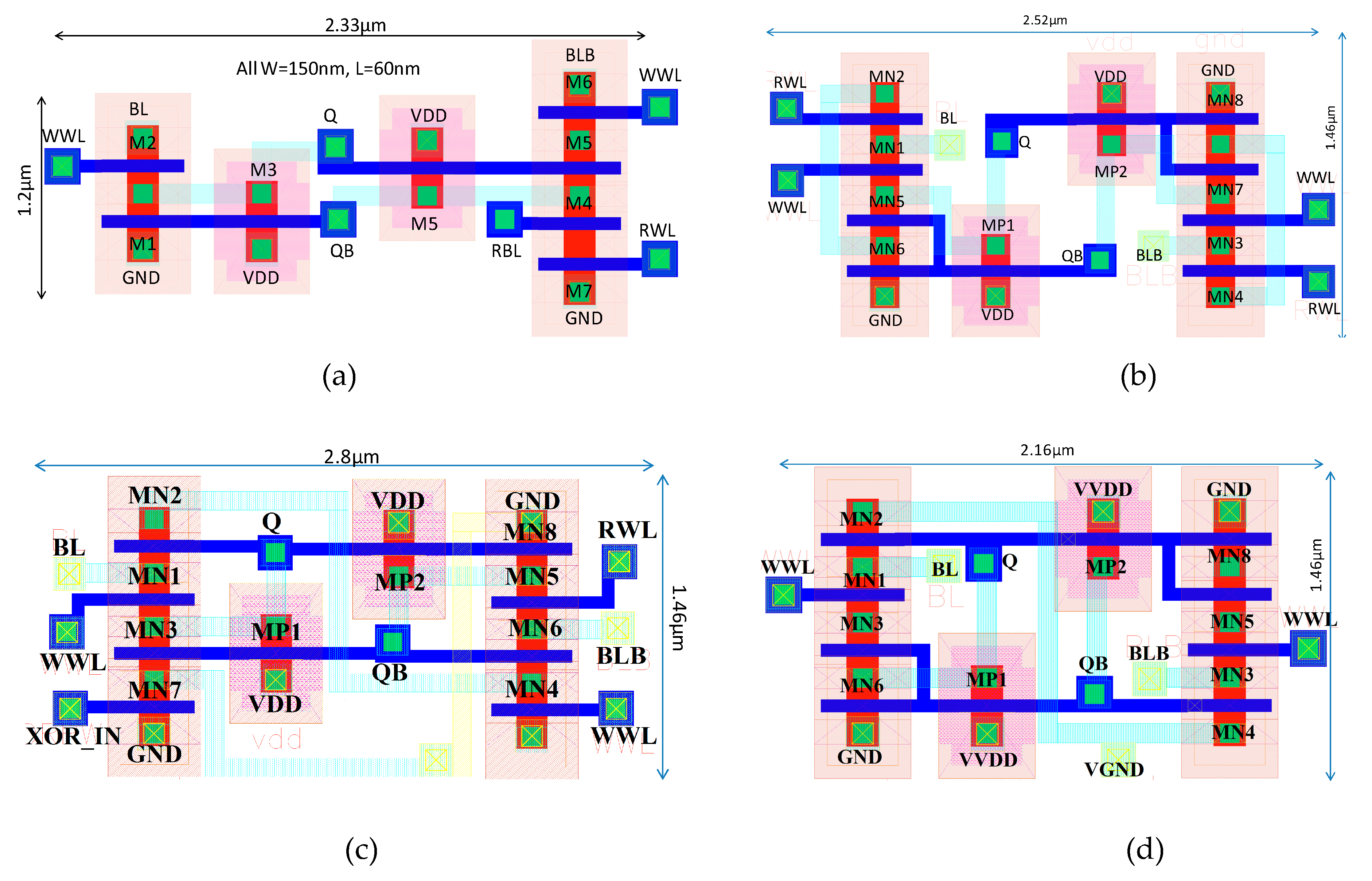
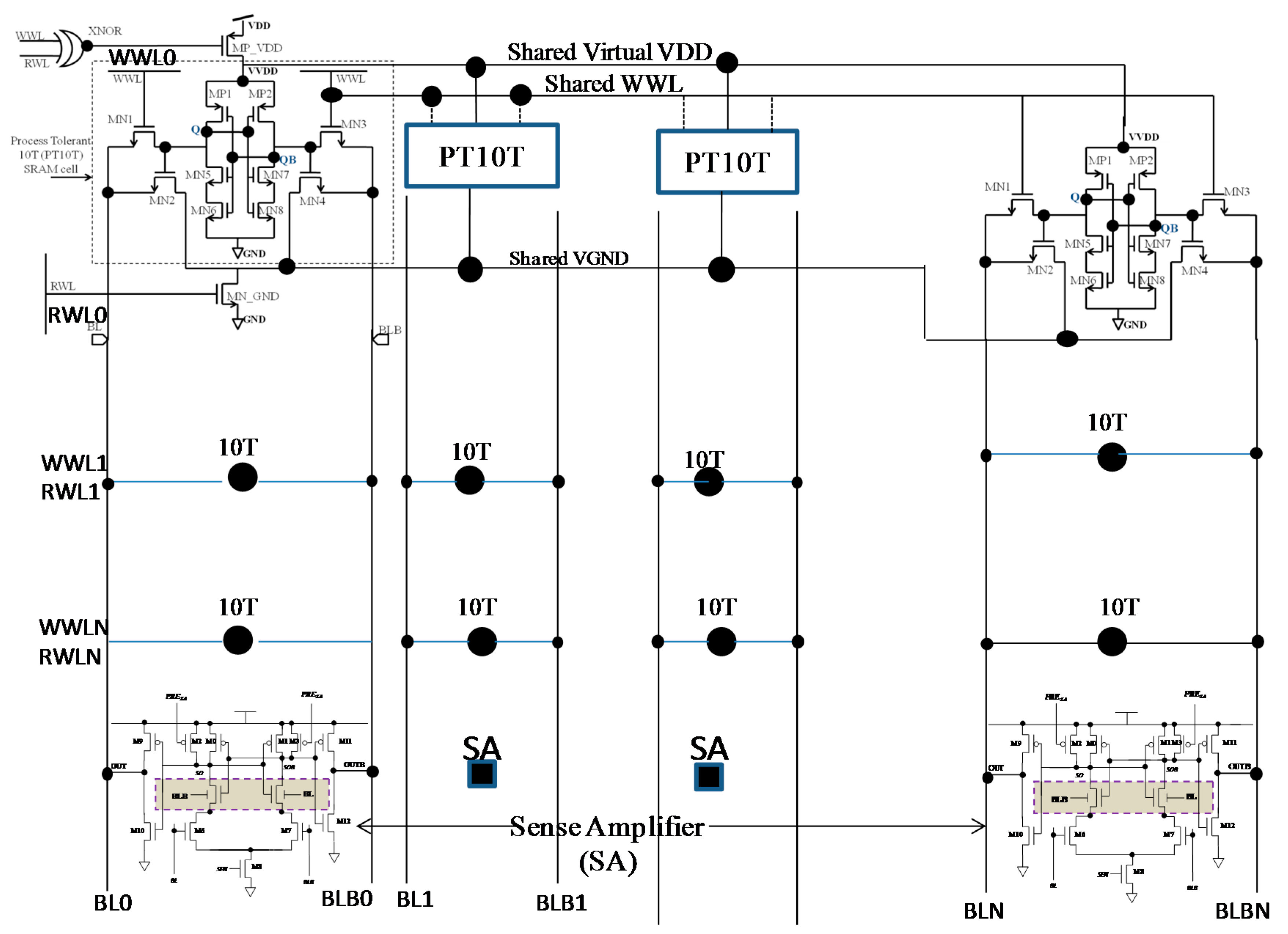
4. 10T SRAM Cell-Based 8 kb Macroblock and Area Overhead

To observe the area overhead and to have a better view of the functionality and placing of SRAM cell and various controlling blocks at array level, a simplified architecture of 10T SRAM array is represented in Figure 3 and the layout area comparison is presented in Table 1. In addition, the functioning of 10T SRAM is explained in Table 2. The table shows the truth table of various operations that take place in the proposed SRAM architecture. The SRAM array uses internal inputs derived from the RWL and WWL signal to control the power-gated p-MOS transistor. However, the proposed SRAM array in Figure 3 shows the complete correlation between various controlling signals and exhibits the procedure of writing and reading using a high-speed differential current compensation sense amplifier (DCC-SA) [14,15,16]. The layout areas of different SRAM architectures are shown in Figure 2 and a comparison between cell areas is shown in Table 1. It is observed that the proposed SRAM has a 17% and 27% reduction in footprint area as compared to ST10T [8] and LP10T [13] SRAM, respectively. In addition, leakage power is also drastically improved due to power gating of supply voltage VDD using MP_VDD transistor. By combining the advantages of both ST10T (using stacked n-MOS transistor) and LP10T (using a separate read path), we addressed a significant improvement in static noise margin and leakage power at different process, voltage, and temperature (PVT) conditions in sub-threshold supply voltages. However, an extra amount of overhead is required at array level to improve leakage power and noise margins at different PVT conditions. Figure 3 shows the overhead area over the SRAM array by introducing two extra transistors at each row of the macroblock. MP_VDD (p-MOS) and MN_GND (n-MOS) are the two overhead transistors included at each row to improve leakage power and read RSNM, respectively. An XNOR gate is also introduced at each row of the SRAM Macro to provide a sleep input to the power gated p-MOS transistor MP_VDD. The XNOR gate has four MOS transistors (two n-MOS and two p-MOS) integrated at each row of the array. These extra transistors bear a channel width of 2 µm, which is 13.33× more than that of the SRAM MOS transistors width (150 nm). Consequently, Table 3 shows the comparison between the areas of 8-Kb SRAM array created by C6T, RD8T LP10T, ST10T, and PT10T SRAM. From the table it is observed that the proposed cell has 35% and 12.5% higher macroblock area as compared to C6T and RD8T, respectively. On the other hand, the proposed 10T SRAM has 17% and 27% less macroblock area as compared to ST10T and LP10T, respectively.

5. Operations and Working of 10T SRAM
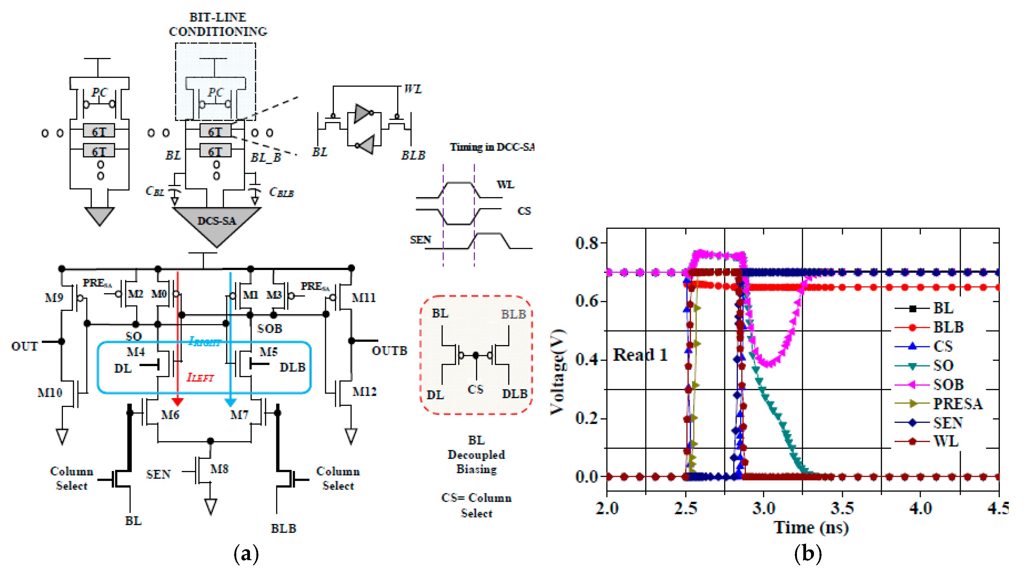
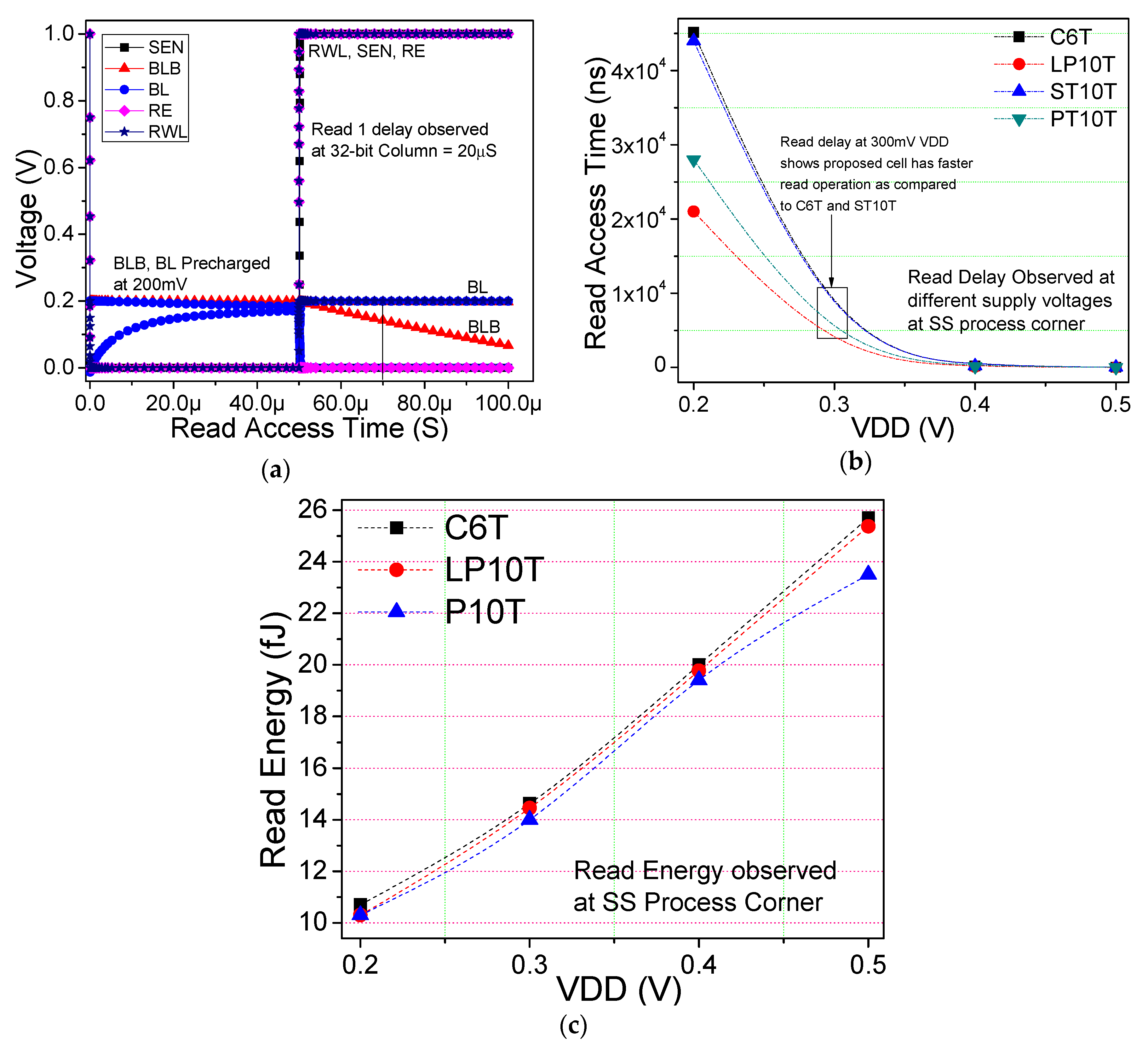
This section demonstrates the working principle of the proposed 10T SRAM in subthreshold operations. Furthermore, the operation has been performed in an 8 kB SRAM macroblock. The read and write operations have been carried out using a 64-bit column.

5.1. Read Operation

Before reading the information, BL and BLB are precharged to VDD using the precharge logic. The read operation is obtained through ultra-fast differential current compensation sense amplifier (DCC-SA) [14,15,16]. The read operation is performed by keeping the read word line (RWL) to HIGH and the write word line (WWL) to LOW and XNOR_I/P at LOW value. For read ‘1’ operation, logic 1 is stored at the storage node Q and RWL is kept HIGH, which eventually turns ON MN_GND and MN2. This forms a discharging path across BL-MN2-MN_GND and a voltage difference, ΔVBL = {(VDD (VBLB) − (VDD − Iread, BL × RMN2-GND)} appears between the BL and BLB line, which is sensed by the full swing inverter sense amplifier [14,15,16]. Iread is the cell current and RMN2-GND is the resistance through MN2 and MN_GND. The read access time is measured as the time between when the RWL signal is activated and the BLB is discharged to the minimum required potential needed by SA to read. The sensing voltage ΔVBL required for DCC-SA is 80 mV [14]. The read access time and power is measured across a 64-bit column of the SRAM cell. The parasitic capacitance of SRAM column is measured after RC-extraction in Cadence layout design at 65 nm UMC Technology. The read operation is achieved using DCC-SA. The sense amplifier works well in subthreshold or near-threshold voltages ranging from 0.3 V to 0.7 V. The circuit topology of DCC-SA is shown in Figure 4a and the simulated transient voltage at 0.7 V VDD is shown in Figure 4b. Figure 4b shows the workings of SA: as soon as SEN and RWL gets activated and chip select (CS) is HIGH, the SA detects the voltage difference (sensing voltage) between BL and BLB. The moment the voltage difference reaches the required sensing voltage, the output node SOB gets logic HIGH, which redirects that logic ‘1’ stored at storage node Q of the SRAM. Moreover, the read operation of proposed cell is shown in Figure 5a.

5.2. Write Operation

For the write operation, WWL must be kept HIGH and RWL is at LOW. However, by making WWL (HIGH) and RWL (LOW), XNOR_OUT is switched to LOW value. The logic 1 is written to storage node Q through BL-MN1-Q, as shown in Figure 5b. However, the write ‘1’ access time is measured as the time between when WWL signal is activated and reaches its VDD/2 value and storage node Q reaches 90% of VDD value. Similarly, write ‘0’ time is measured as the time between when the WWL signal is activated and reaches its VDD/2 and storage node Q reaches to 10% of VDD. The half-select issue in write operation is also taken care of by putting a WE signal at each column of SRAM array, as shown in Figure 3. By separating the read and write paths using WE and REB, the sensing and writing operations can be separated, which eventually helps to negate the half-select read and write issue.

5.3. Data Retention

In the proposed SRAM a coarse-grain power-gating technique is used, which will turn OFF the power gated p-MOS connected to VDD in standby mode and reduces the overall leakage power. However, during read and write operations in power gated logic, the power switch (VDD) must provide adequate supply voltage and current to the SRAM cells to maintain the hold stability and the bit information at storage node. During standby, the VDD gets turned off using power gated p-MOS (MP_VDD) transistor and the SRAM cell gets connected to VVDD. The VVDD is set to a required value less than VDD, which will maintain the hold states so that the SRAM can access its stored information in read operations.
In general, the memory cell remains in a static or holding state most of the time. Therefore, there would be a very high possibility of an increase in leakage power in a SRAM cell in different PVT conditions. In the proposed PT10T SRAM, the control signal XNOR_OUT turns OFF MP_VDD, which helps to reduce the leakage current by disconnecting the path of the latch from VDD to GND. However, the leakage power in the C6T SRAM cell is introduced due to the non-availability of a virtual VDD transistor such as MP_VDD. In C6T and RD8T SRAM cells, there is a potential difference of VDD between pull up (PU) and pull down (PD) transistors [18]. Therefore, the leakage current flow is higher in C6T and RD8T SRAM cell. However, in proposed cell, due to the power gating of VDD, the virtual node VVDD is now set at a positive voltage [19] lower than VDD. This eventually reduces the hold static noise margin (HSNM) but improves the leakage power essential for IoT edge device, as shown in Figure 6.

6. Simulation Results of PT10T SRAM

The proposed 10T SRAM is simulated in 65 nm standard CMOS technology. Post-layout simulation at 6-sigma (σ) process variations are observed and compared with C6T, RD8T, ST10T [8], and LP10T [13] SRAMs to determine various constraints like leakage power, read–write delay and power, power delay product (PDP), read static noise margin (RSNM), dynamic read margin (DRM), write static noise margin (WSNM), and write trip point (WTP).

6.1. Simulation Setup

The simulation setup is observed through Monte Carlo post-layout simulations on an 8 Kb SRAM array. The read–write access time and power is measured by applying a write and read operation at a single column of the array. The proposed SRAM Macro has a 64-bit column coupled with a DCC-SA. The DCC-SA takes a small differential positive sensing voltage as an input and attains an output that is equivalent to the information stored in the SRAM cell. To perform read and write operations, access transistors are used to separate the read and write paths. The row and column decoder are used to activate the WWL and RWL of the Marco. The setup for all operations is observed at the worst-case process corner. The write and read operations are performed through BL and BLB. While reading the information from the SRAM, the bit-lines are pre-charged to VDD using a pre-charge signal. Furthermore, all the observations are performed using 1000 Monte Carlo simulations.

6.2. Write and Read Analysis

The write ‘1’ access time is measured as the time when WWL signal is triggered and the storage node Q reaches 90% of VDD. Similarly, write ‘0’ access time is defined as the time when WWL signal is activated and storage node Q reaches 10% of VDD. The write power is measured as the product of average current dissipation and the source voltage until write is achieved. Additionally, Figure 7a,b show the write ‘1’ and write ‘0’ delay, respectively, observed at different supply voltages in worst-case (SS) process corner (PC). The delay of LVT PT10T SRAM is compared with existing LVT C6T, RD8T, LP10T [13], and LP9T [12], which shows that PT10T SRAM has a similar write access time. Similarly, Figure 8a,b show comparisons of write ‘0’ and write ‘1’ power, respectively, at different supply voltages in fast-fast (FF) PC. The results obtained show that the proposed LVT PT10T has an improvement in write ‘1’ power by 8.5%, 12.6%, 19.35%, and 19.3% as compared to LVT C6T, RD8T, LP10T [13], and LP9T [12] SRAM, respectively, at 0.3V VDD. The outcome illustrates a reduction in write ‘0’ power by 5.2%, 1%, 10%, and 6.6% as compared to LVT C6T, RD8T, LP10T, and LP9T SRAM, respectively at 0.3 V VDD.
Furthermore, Figure 9 shows the comparisons graphs of energy consumption of various SRAM cells at different supply voltages at SS and FF process corner in write ‘0’ and write ‘1’ operation. The results of LVT PT10T SRAM show a reduction in write ‘1’ energy by 1.23%, 14%, and 20% as compared to LVT RD8T, LP10T, and LP9T SRAM, respectively, at 0.3 V supply voltage. However, write ‘0’ energy is improved by 1%, 6.2%, and 5.2% as compared to RD8T, LP10T, and LP9T SRAM, respectively, at 0.3 V VDD. Furthermore, the read access time is measured when RWL is activated and pre-charged bit-lines (BLs) discharge and reach the minimum sensing voltage required by SA [14,15,16]. From the DCC-SA architecture presented in [14], it is observed that a differential sensing voltage of 80 mV is required to read data from SRAM. Figure 10a shows the simulation states of SRAM at read time. The read access time of proposed SRAM is compared with the existing SRAM cells, as shown in Figure 10b. In addition, the read power is measured until the differential voltage across bit-lines reaches the sensing voltage. Figure 10c illustrates the comparisons of read energy. It is observed that the read access of proposed LVT 10T SRAM is 1.6× and 1.57× faster than C6T and ST10T [8], respectively, in SS PC at 0.3 V VDD. In addition, the read energy of proposed cell is reduced by 4% and 3% as compared to LVT C6T and LP10T SRAM, respectively, in SS PC at 0.3 V VDD.

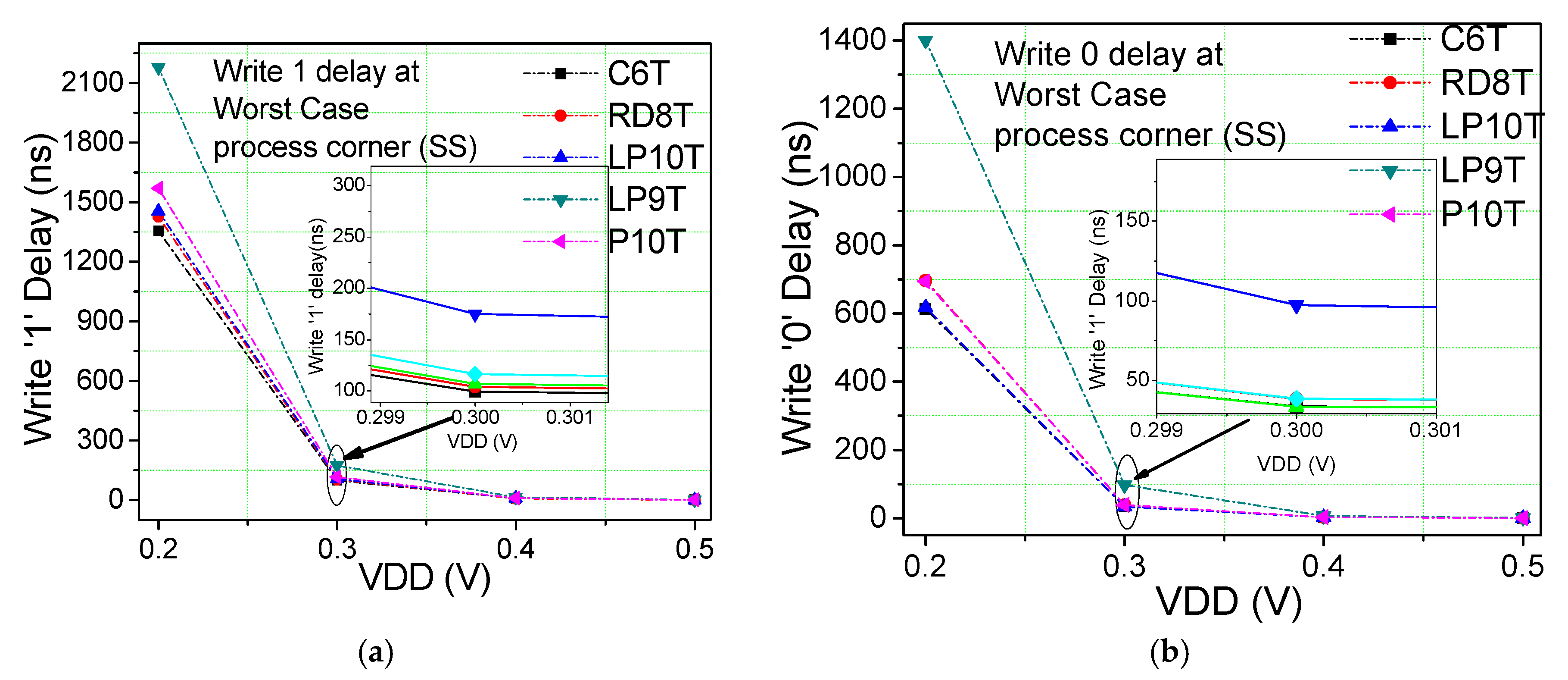
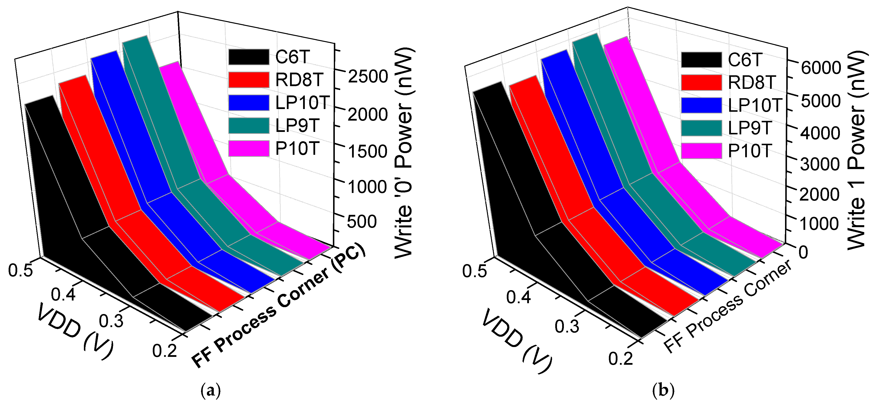
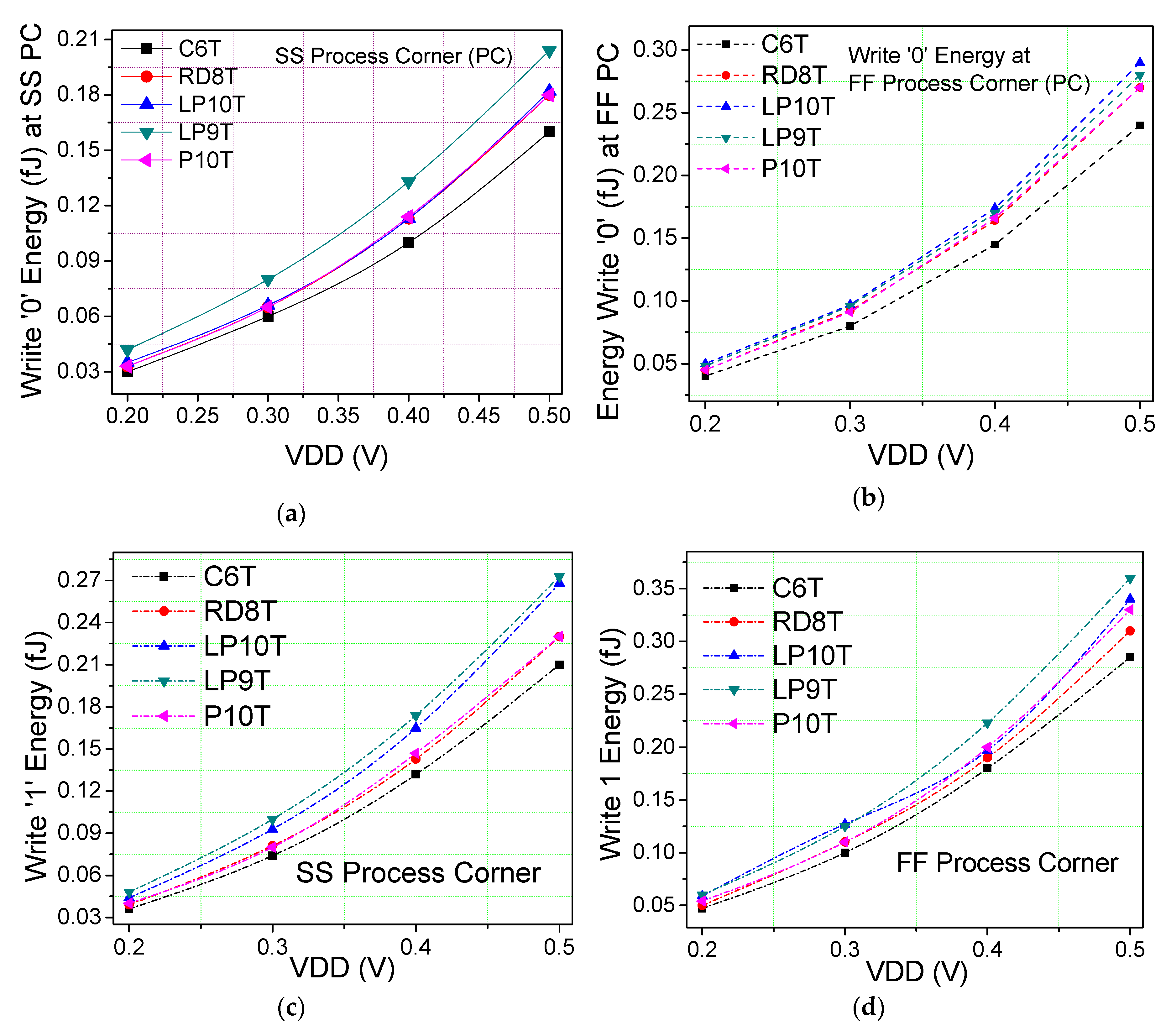
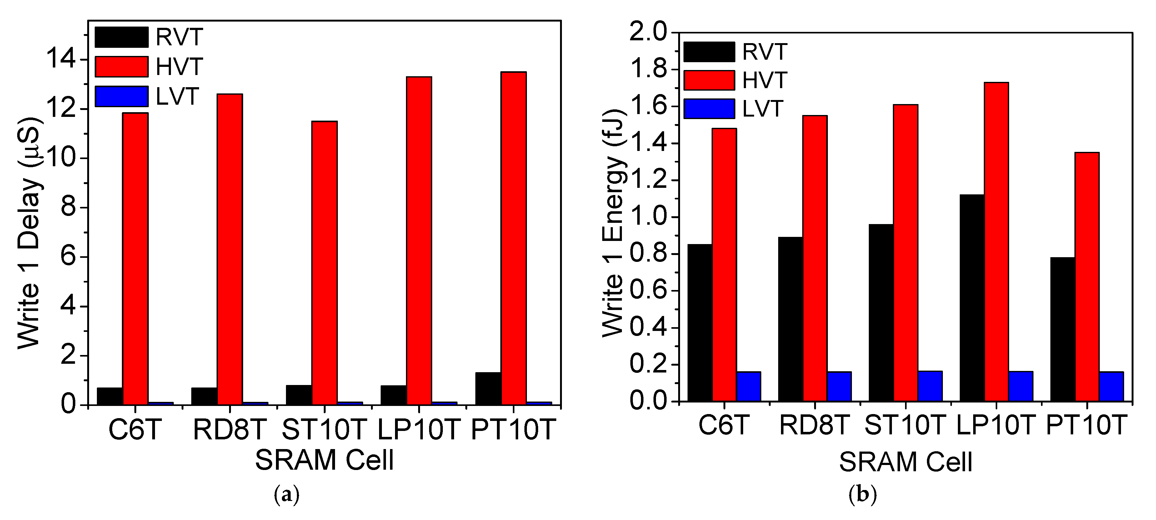
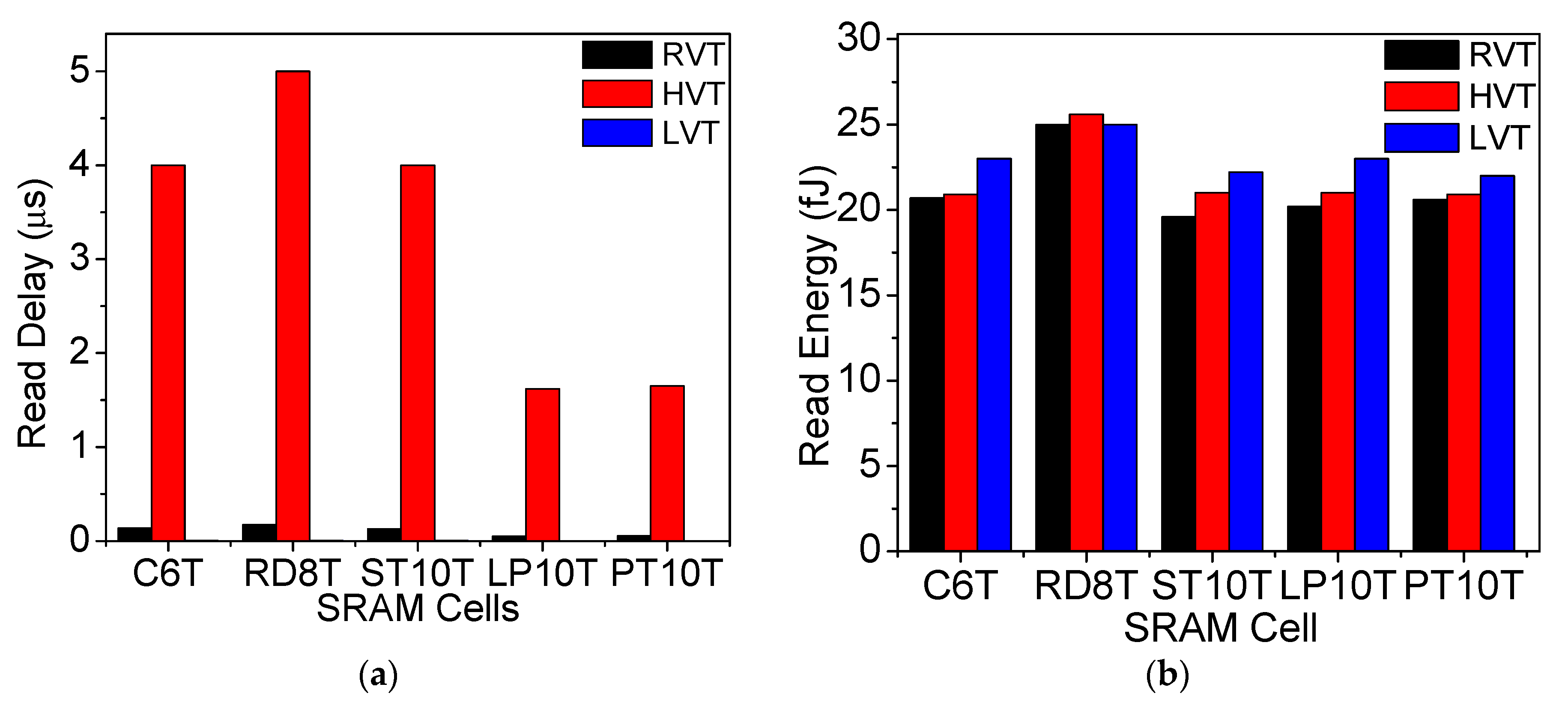
6.3. Write and Read Analysis at Different Threshold Voltage Transistors

The various merits of write and read operations of proposed 10T SRAM and other existing SRAMs are analyzed using high-threshold HVT, standard-threshold RVT, and low-threshold LVT MOS transistors. The bar graphs shown in Figure 11a,b demonstrate the comparison between write access time and write energy, respectively, using different threshold voltage transistors at 0.3 V VDD. Due to stacked n-MOS transistors in SRAM latch and gated p-MOS transistor at VDD, the results in Figure 11a show a higher write access time for proposed PT10T SRAM as compared to other existing memory cells. However, the power gating at VDD reduces the write energy in RVT-and HVT-based PT10T SRAM, as shown in Figure 11b, while the LVT SRAMs shows similar write energy values. The write energy of proposed HVT 10T SRAM has reduced by 43%, 46%, 44%, and 52% as compared to HVT C6T, RD8T, ST10T, and LP10T SRAM, respectively.
Further, Figure 12a,b illustrates the read access time and read energy, respectively, at 0.3 V VDD. Figure 12a show that the proposed cell has a fast read access (similar to LP10T) due to introduction of virtual ground n-MOS transistor (MN_GND) with high channel width (W = 2 µm) compared to other existing SRAMs measured using threshold voltage transistors. The read delay of proposed RVT 10T SRAM has reduced by 61.6%, 69.5%, and 59% as compared to HVT C6T, RD8T, and ST10T SRAM, respectively. However, the read delay of proposed HVT 10T SRAM has reduced by 58.75%, 67%, and 58% as compared to HVT C6T, RD8T, and ST10T SRAM, respectively.

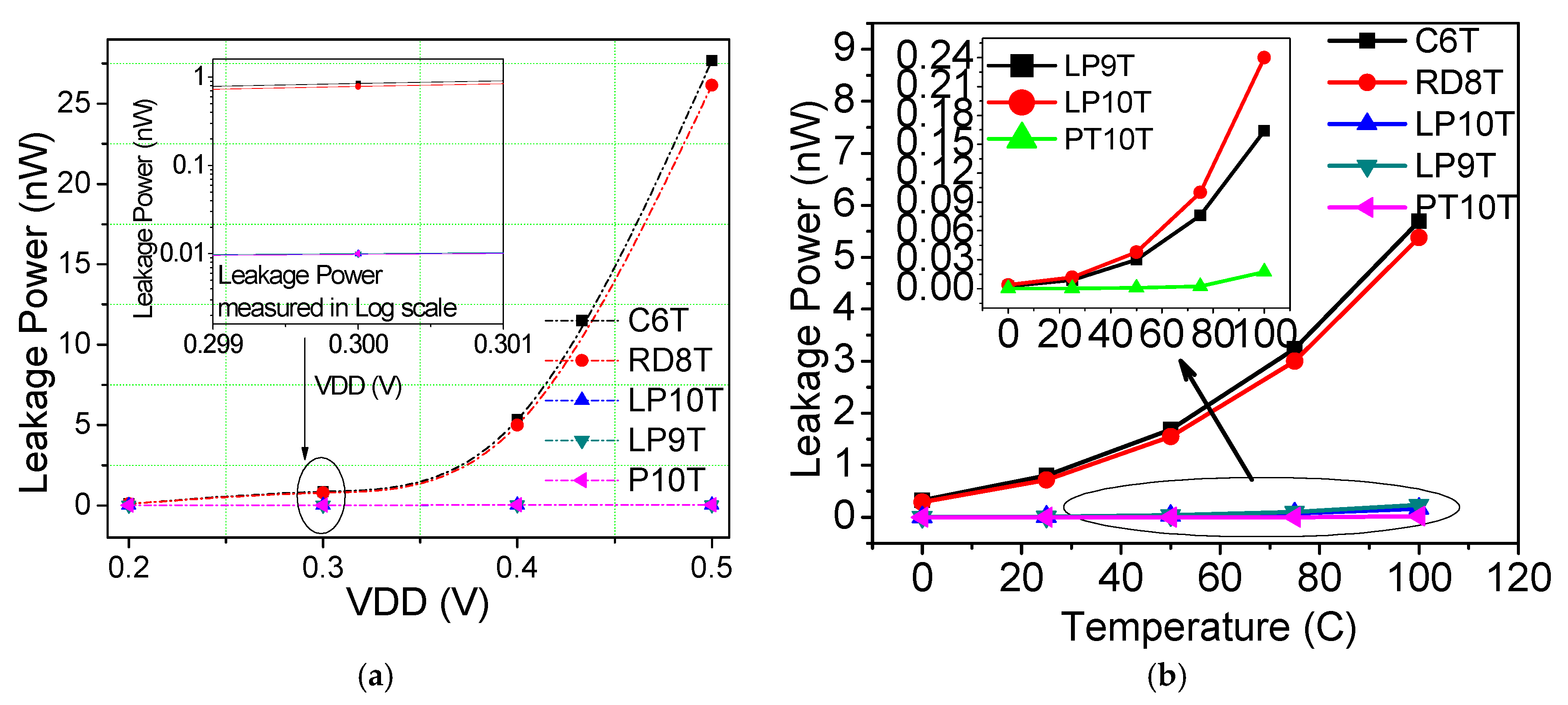
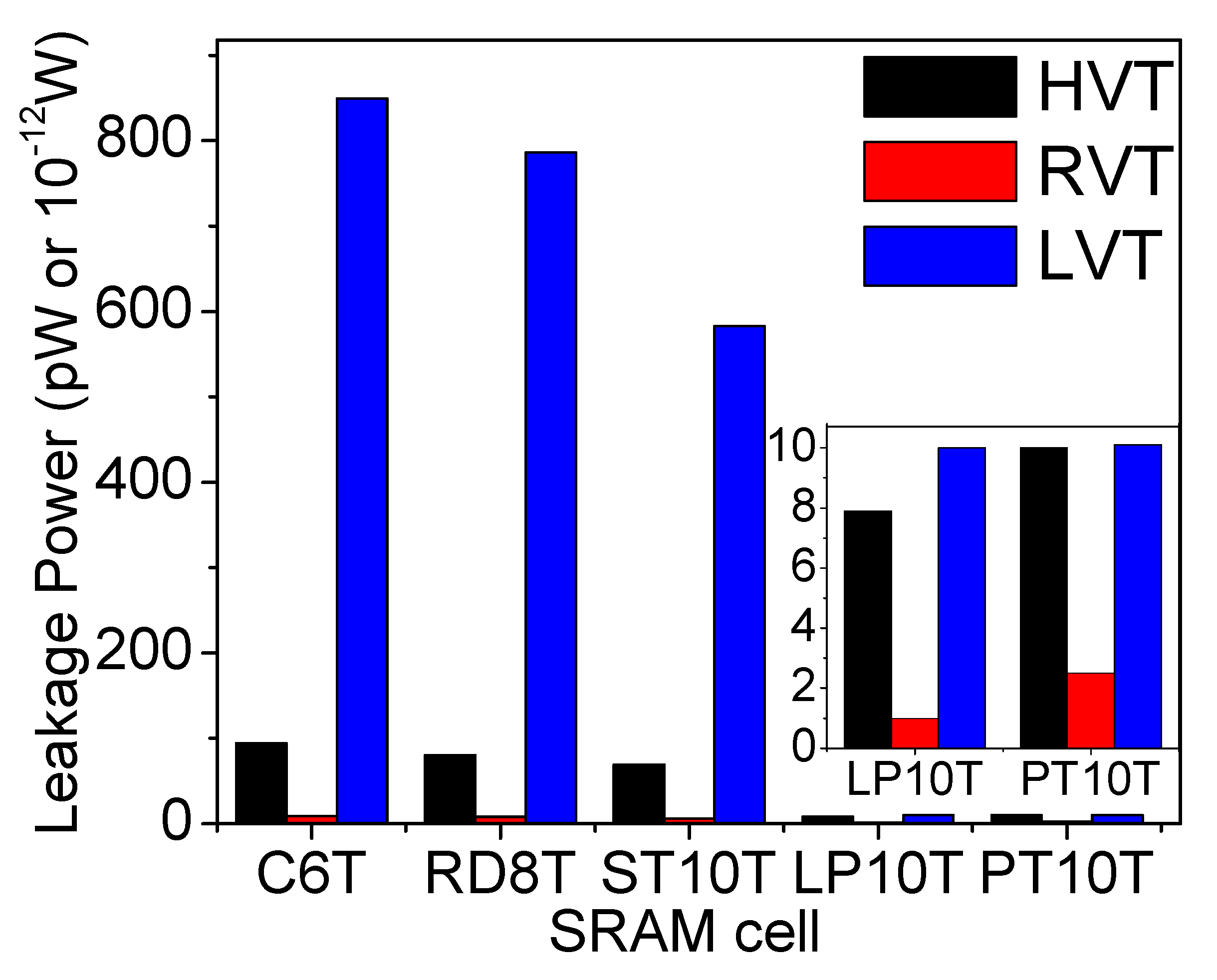
6.4. Standby or Leakage Power

Leakage current is measured while the SRAM cell is in a static or holding condition. The static power or leakage power is the amount of power lost during holding. Figure 13a shows the leakage power variations w.r.t. the supply voltages for proposed LVT PT10T SRAM compared to other exiting LVT SRAMs. The proposed LVT 10T SRAM shows a significant improvement in leakage power (84 nW at 0.3 V VDD) which is reduced by 98.76%, 98.6%, 6.7%, and 98.2% as compared to the LVT C6T, RD8T, LP9T, and ST10T SRAM, respectively, at 0.3 V VDD. However, the outcome of PT10T SRAM (Figure 14) using HVT transistors show a substantial reduction in leakage power/cell by 72%, 68.75%, 92.5%, and 57% as compared to the HVT C6T, RD8T, and ST10T SRAM, respectively.
Furthermore, the leakage power is observed at different temperature values ranging from 0 °C to 100 °C. Figure 13b shows that the proposed PT10T SRAM has a minimum change in leakage power w.r.t. increase in temperature. The results show that PT10T SRAM has superior temperature tolerance as compared to existing SRAM architectures. The invariability in leakage power w.r.t. temperature variations is very convenient for IoT devices operating on battery power due to their high junction temperature and external temperature variation due to climate change.

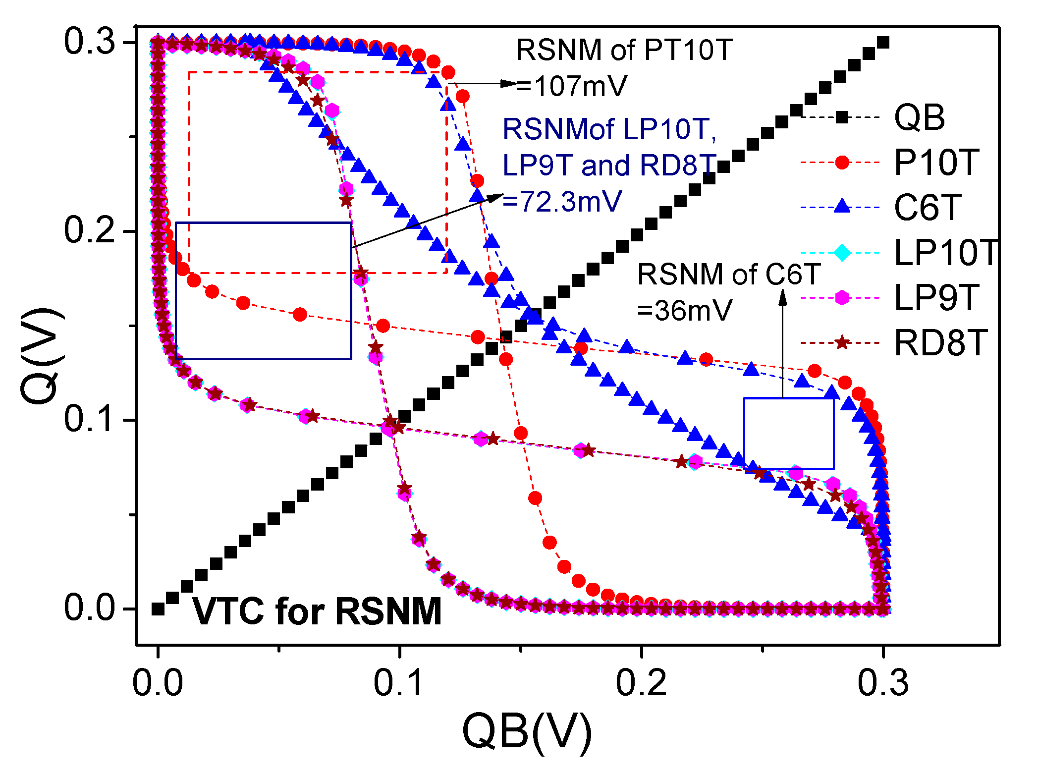
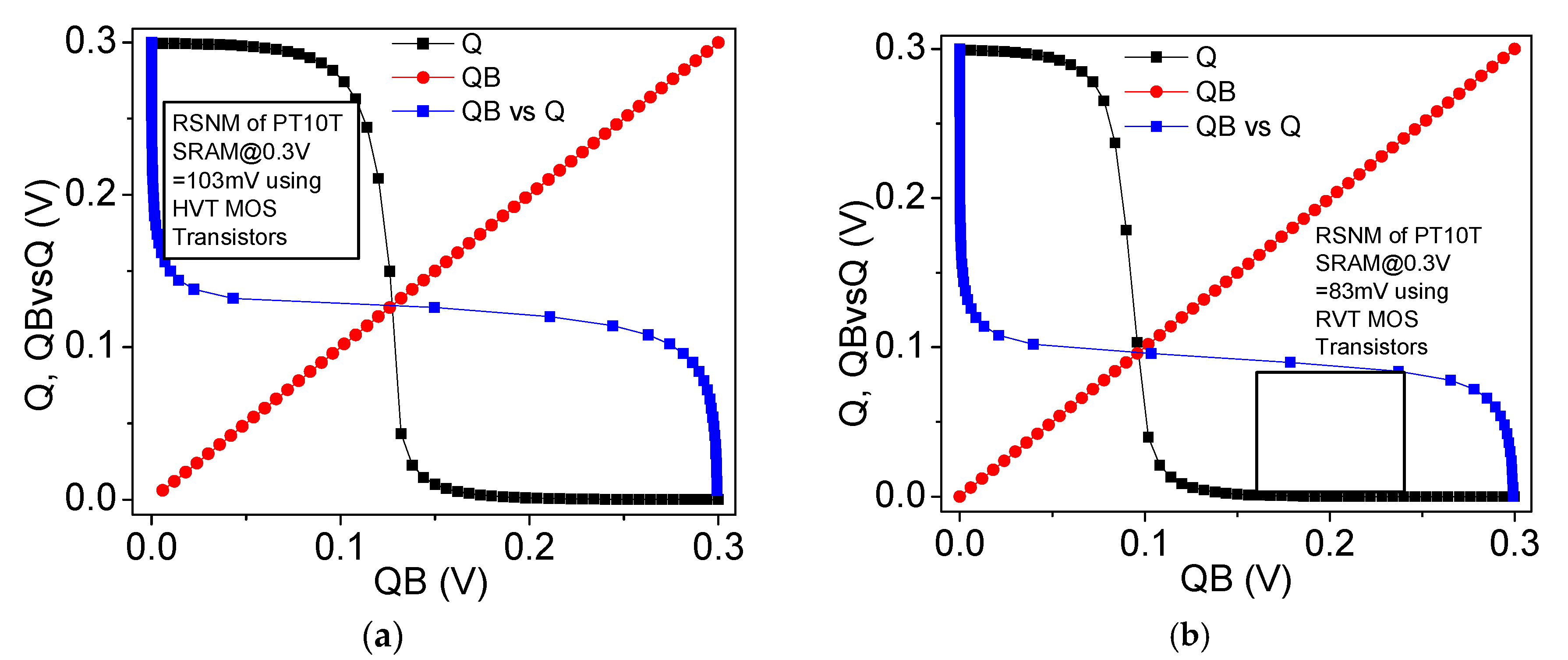
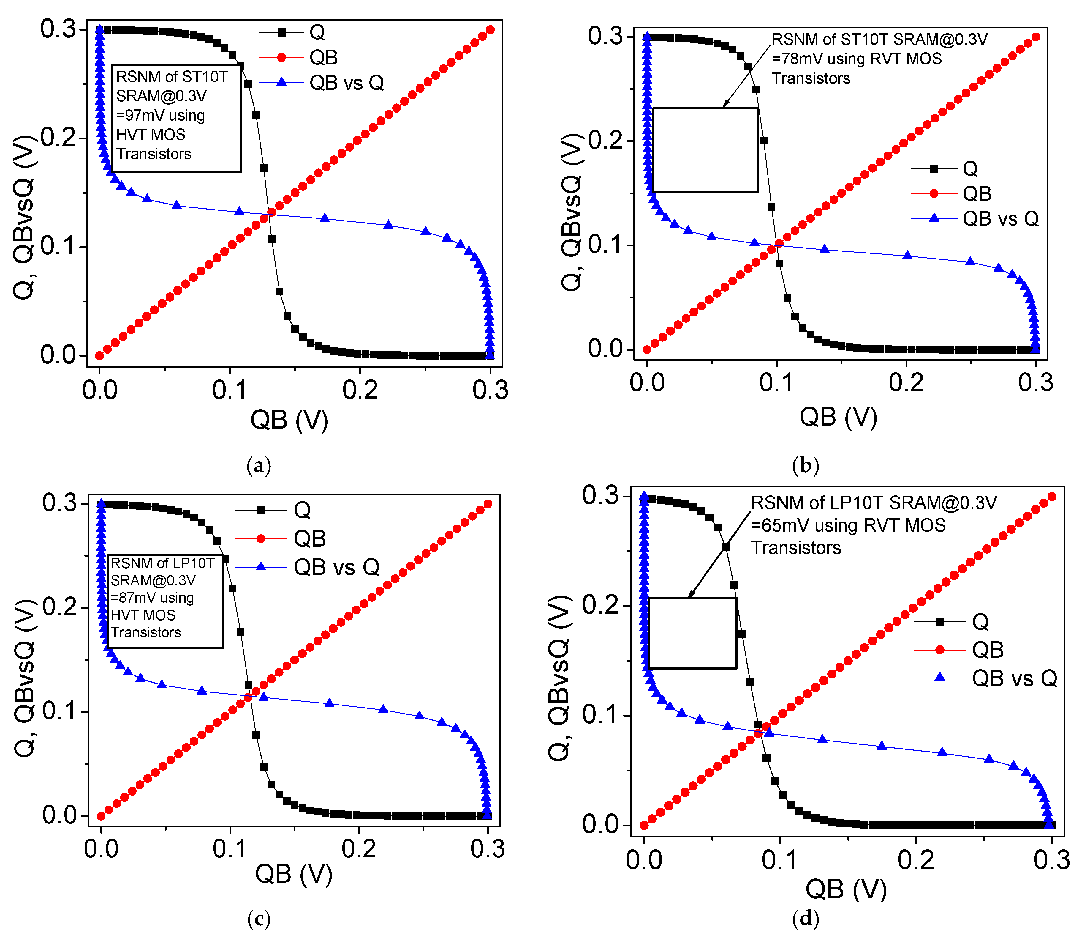
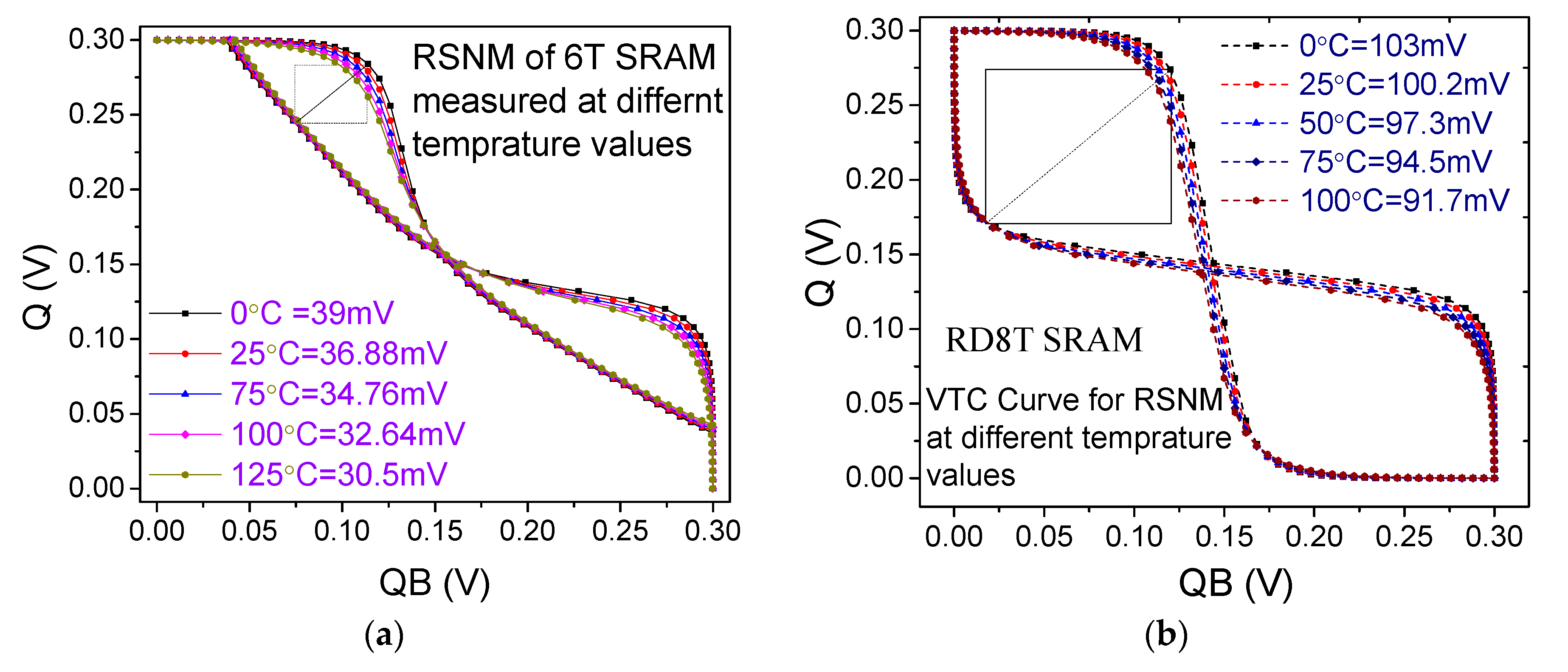
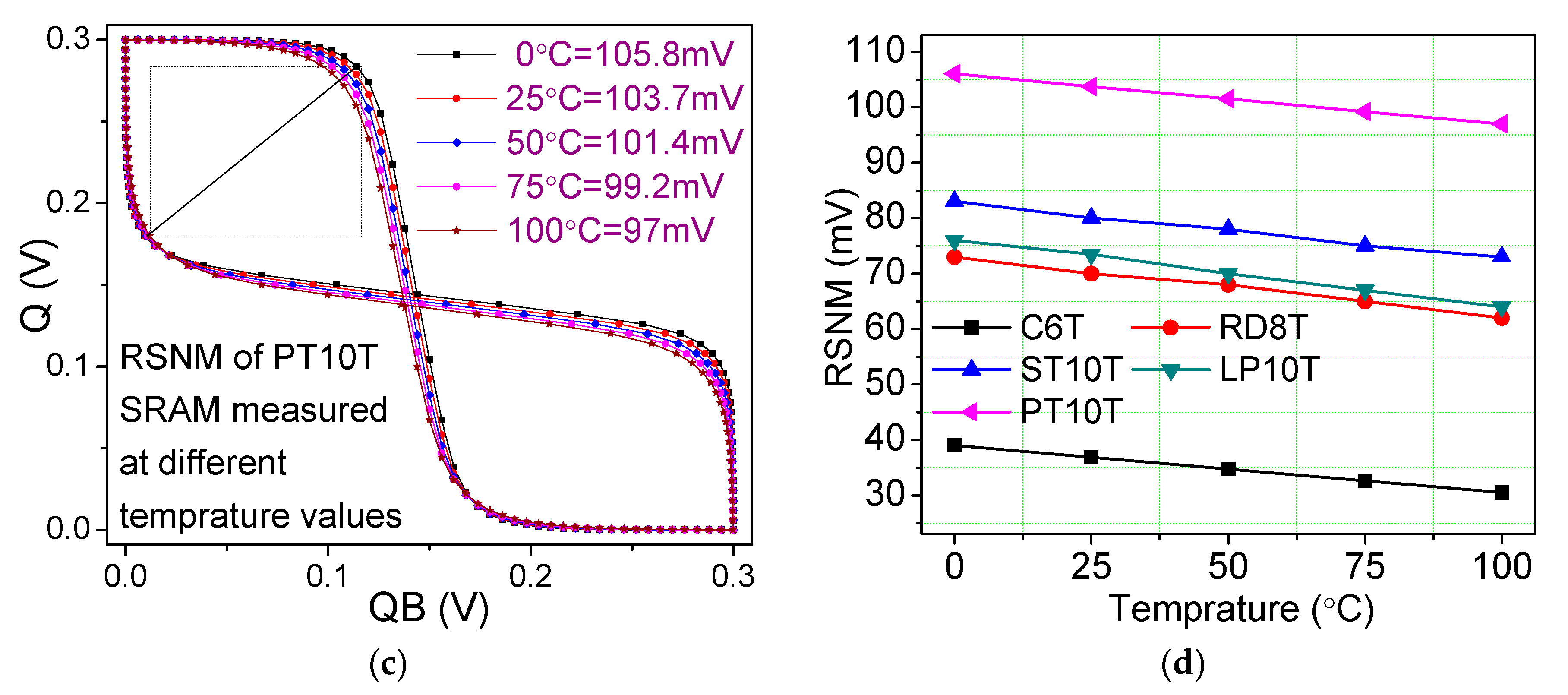
6.5. Read Static Noise Margin (RSNM) and Dynamic Read Margin (DRM)

Read static noise margin (RSNM) is measured by applying a DC noise voltage source at one of the storage node Q or QB and investigating the effect on other storage node. The RSNM is examined in the read operation when RWL is HIGH and WWL is LOW. Due to the separation of read path (BL-MN2-MN_GND) from the latch, it does not affect the storage nodes of the SRAM cell, which would further help to neglect the consequences of static noise and, as a result, improves the RSNM. In Figure 15, the RSNM of the proposed LVT PT10T SRAM cell measured as 107 mV, which has 3×, 1.48×, 1.48×, and 4% higher than LVT C6T, RD8T, and LP10T SRAM, respectively, at 0.3 V VDD. The RSNM of read decoupled (RD)-8T, LP9T and LP10T SRAM analyzed and are identical to each other due to their similar read architecture.
Furthermore, the RSNM of proposed 10T SRAM (Figure 16) is measured using HVT and RVT transistors. Similarly, the RSNM of ST10T and LP10T using HVT and LVT transistors are observed at 0.3 V VDD as shown in Figure 17. From Figure 16a and Figure 17a,c, it is observed that the HVT PT10T SRAM has 6% and 18.4% higher RSNM values as compared to HVT ST10T and LP10T, respectively. Similarly, from Figure 16b and Figure 17b,d, it is observed that the RVT PT10T SRAM has 6.4% and 27.7% higher RSNM values as compared to RVT ST10T and LP10T, respectively.
Furthermore, the butterfly curves for RSNM are observed at different temperature values for C6T, RD8T, and PT10T SRAM, as shown in Figure 18a–c, respectively. In addition, the comparison of RSNM w.r.t. the temperature values are also shown in Figure 18d. The figure shows a tremendous tolerance in RSNM w.r.t. the change in temperature as compared to the existing SRAMs.
Consequently, read margin is measured in a situation where there is no static DC noise to hamper the storage nodes. While measuring read margin, the RWL is activated HIGH and WWL is kept at LOW. The read dynamic noise margin (RDNM) is observed when the bit-line reaches the sensing voltage. Simultaneously, the voltage difference between storage node Q and QB is defined as RDNM. In our case the RDNM value comes out equivalent to 290 mV, which is 7.5% better than C6T SRAM, as shown in Figure 19a,b at 0.3 V VDD.

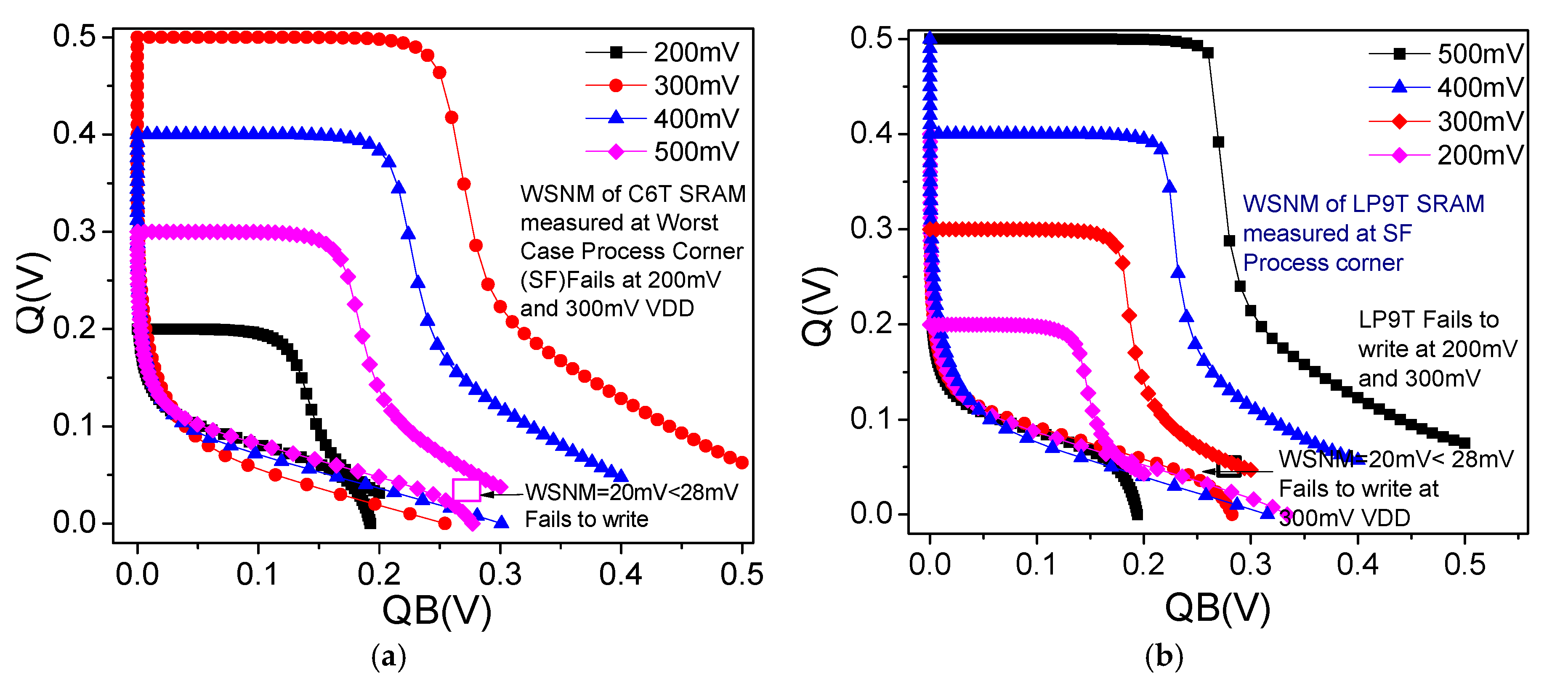
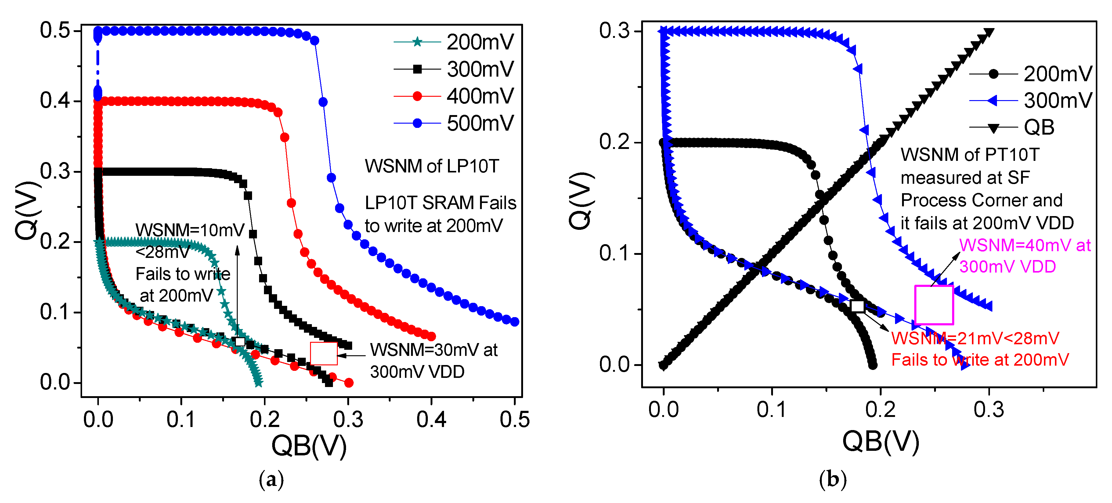
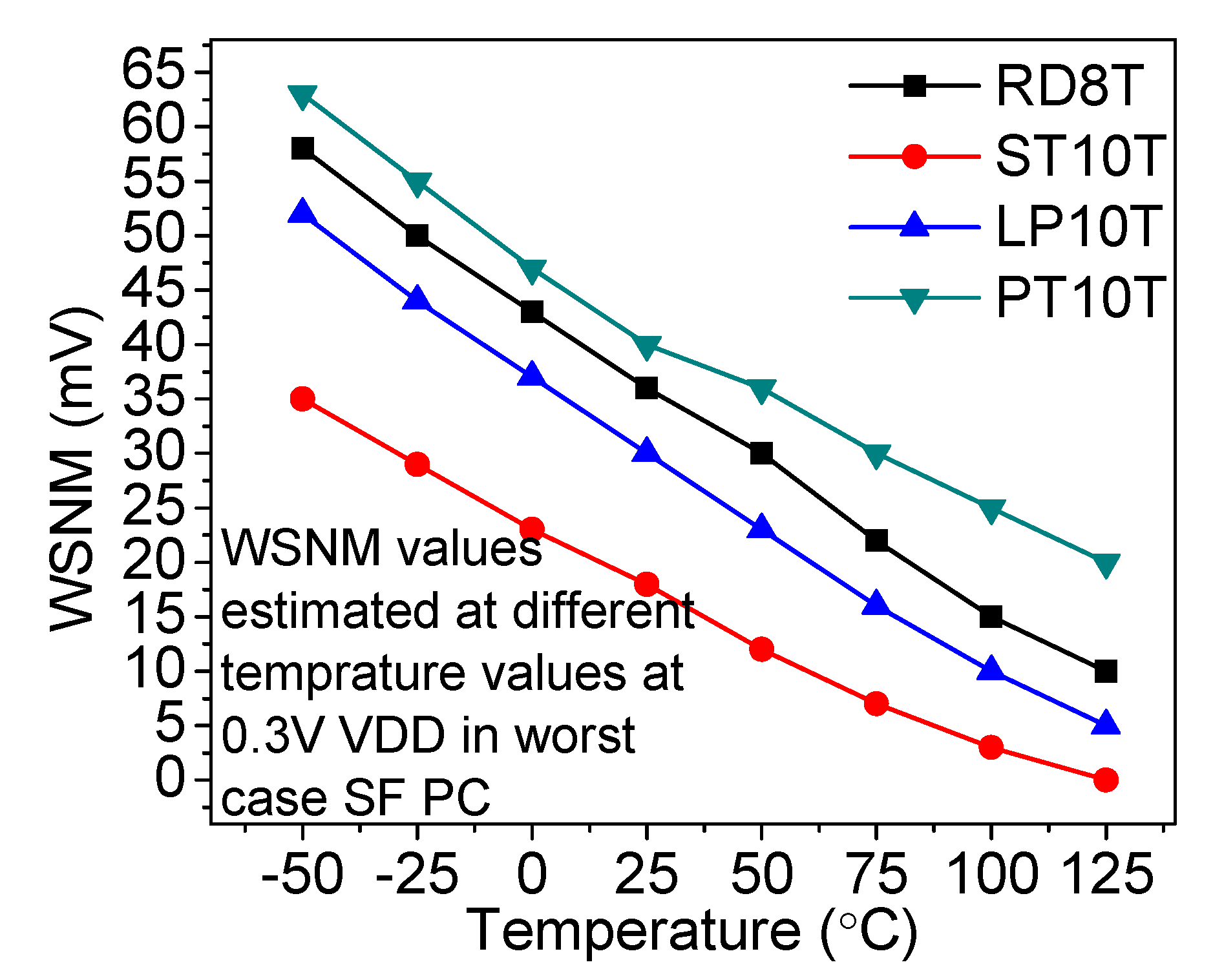
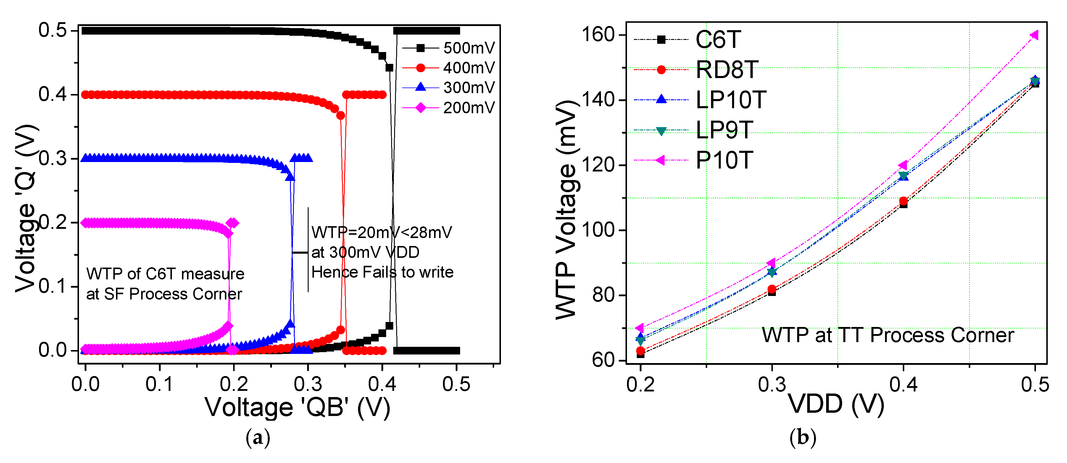
6.6. WSNM and Write Trip Point (WTP)

The write static noise margin (WSNM) is measured at the time of write operation by initiating a linear DC noise at one of the storage nodes and observing the effect of the noise at the other end. The WWL is kept HIGH, while the RWL is LOW. The plots in Figure 20a,b and Figure 21a,b determine the WSNM of C6T, LP9T, LP10T, and PT10T SRAMs, respectively, at worst-case (SF) process corner. Moreover, from Figure 20a,b it is observed that the WSNM of C6T and LP9T SRAM has failed to write at 0.2 V with WSNM (20 mV) less than the thermal voltage (28 mV). In addition, LP10T has a WSNM of 10 mV and 30 mV at 0.2 V and 0.3 V VDD, respectively. Therefore, it fails to work at 0.2 V and has a near-threshold value at 0.3 V (WSNM = 30 mV). Consequently, it is suggested to operate LP10T SRAM above 0.3 V supply voltage. Furthermore, the proposed 10T SRAM has a WSNM of 21 mV and 40 mV at 0.2 V and 0.3 V VDD, respectively, in SF PC. From the results, it is recommended not to operate at 0.2V VDD; nevertheless, there is significant activity at 0.3 V VDD. The WSNM of PT10T shows 2×, 2×, and 1.5× higher outcomes as compared to C6T, LP9T, and LP10T SRAM, respectively, at 0.3 V VDD.
Moreover, in Figure 22 the WSNM of proposed 10T SRAM and other SRAM are observed under different temperature values at 0.3 V. The WSNM of proposed SRAM, measured at worst-case process corner, ranges from 20 mV to 63 mV with changes in temperature. It can be observed from the figure that the proposed cell shows the best performance in terms of WSNM as compared to existing SRAMs. Additionally, the write trip point (WTP) is viewed as a key parameter in SRAM write ability. It is measured by lineally varying WWL from 0 to VDD and at the same time writing single-bit information through Bitlines [20]. Furthermore, the WTP is measured at the crossover point of Q and QB, as shown in Figure 23a, as a difference between VDD and voltage at the crossover. However, the WTP is compared at different supply voltages in the TT process corner, as shown in Figure 23b. It shows that the proposed SRAM has 11%, 9.75%, 3.3%, and 3.4% better WTP as compared to C6T, RD8T, LP10T, and LP9T SRAM, respectively at 0.3V VDD.

6.7. Comparison to FinFET-Based SRAM

To reduce the threshold variations in bulk-CMOS, FinFETs are extensively used in sub nanometer technologies to reduce the threshold variations in bulk-CMOS [21,22]. The main advantage of FinFET device is that it reduces the random dopant fluctuation (RDF), which is the key reason behind the threshold voltage variations in ultra-low voltage (ULV) operations. Although FinFET devices have many benefits, FinFET based C6T SRAM does not provide sufficient yield required in the subthreshold region. Additionally, it is not easy to improve read and write stability in ULV operations. In addition, for more analysis of FinFET based SRAM, Younghwi et al. [22] presented FinFET C6T, RD8T, and ST10T SRAM architectures in 14 nm Technology. The results in Table 4 show that FinFET-based SRAM design has very high read and write access speed as compared to the proposed bulk CMOS-based PT10T SRAM. However, the major constraints on today’s IoT devices are the leakage power and energy, not the speed. From Table 4, it can be observed that Bulk-CMOS still emerges as the paramount technology of choice considering application in low-power and -energy devices.

6.8. Inter- and Intra-Die Variations

Sources of parametric variation are separated into two types, inter-die and intra-die [23,24]. Since the variation within the die due to layout pattern dependencies may be larger than variations across wafer, the matching of devices is different on one chip vs. on one wafer. The structural or electrical parameter (P) such as W, Tox, Vth, channel mobility (µ), coupling capacitances, and line resistances have dependencies on inter-/intra-die variations, as shown below:
P   = P 0 + Δ P 1 + Δ P 2 + Δ P E
where P0 is a nominal design value and ∆P1 is the intra-die variation (within a given chip). ∆P2 is the inter-die variation (from one chip to another). ∆PE is the remaining random or unexplained variation. Intra-die variation is the deviation occurring spatially within any one die [23]. In contrast to inter-die variation, intra-die variation contributes to the loss of matched behavior between structures on the same chip. Additionally, to compute the effect, Monte Carlo (MC) simulations for 1000 samples considering inter-/intra-die random variations were performed at 0.3 V supply voltage in worst-case process corner. The parameters such as write access time, read access time, RSNM, and WSNM are observed at inter/intra die variations. Furthermore, Table 5 and Table 6 show the comparison of various parameters of C6T, RD8T and proposed 10T SRAM at inter-/intra-die variations.

7. Summary of Results

Table 4 shows the summary of post-layout simulation results of proposed PT10T 8-Kb SRAM at 0.3 V power supply. The parameters are observed at 27 °C (room temperature) in the worst-case process corner. Table 4 shows that the leakage power of proposed LVT 10T SRAM is reduced by 98.76%, 98.6%, 6.7%, and 98.2% as compared to the LVT C6T, RD8T, LP9T, and ST10T SRAM, respectively, at 0.3V VDD. The WSNM value is improved by 2×, 25%, 2×, 33.33%, and 14.3% as compared to C6T, RD8T, LP9T, and ST10T SRAM, respectively, at worst-case (SF) process corner. The RSNM is enhanced by a factor of 3×, 1.48×, 1.48×, 1.48×, and 3.88% as compared to C6T, RD8T, LP9T, LP10T, and ST10T SRAM at TT process corner, respectively. The dynamic read margin is determined at the time of read operation and shows improvement by 31.8% and 8.2% as compared to C6T and ST10T SRAM, respectively. Moreover, the WTP is also improved by 11.11%, 9.75%, 3%, 3%, and 9.75% as compared C6T, RD8T, LP9T, LP10T, and ST10T SRAM, respectively at TT process corner. The write ‘1’ energy is reduced by 6%, 2%, and 6% as compared to LP9T, LP10T, and ST10T SRAM, respectively, at worst-case (SS) process corner at 0.3 V VDD. However, the read ‘1’ energy is reduced to 4.3%, 12%, 6.4%, 4%, and 1% as compared to C6T, RD8T, LP9T, LP10T, and ST10T SRAM, respectively, at worst-case (SS) process corner at 0.3V VDD. On the other hand, the footprint area of the proposed cell has 35% and 12.5% more overhead as compared to C6T and RD8T SRAM, respectively. In addition, the proposed 10T SRAM has 17% and 27% lesser macroblock area as compared to ST10T and LP10T, respectively. Therefore, the proposed 10T SRAM is an attractive choice for today’s battery-operated IoT enabled system on chip (SoC) applications, where the leakage power consumption and the cell stability are of primary concern.
Furthermore, Table 6 shows a comparison table of all of the fundamental parameters measured using different threshold voltage transistor (HVT, RVT, and LVT). The inter-die and intra-die process/mismatch variations are considered at 0.3 V power supply and room temperature. All of the parameters are measured at worst-case process corner. From the table it can be observed that the proposed 10T SRAM shows the best performance in terms of write power, read–write energy, leakage power, RSNM, and WSNM. The objective of this paper towards creating memory architecture for ULP IoT applications can be achieved by introducing low leakage, high stability, and low read–write energy PT10T SRAM.

8. Conclusions

This paper exhibits a robust ULP process-tolerant 10T SRAM cell for IoT applications. The low-voltage operations lead to concern about process variations in subthreshold SRAM design. However, the low leakage and high read–write stability at different PVT variations make the proposed cell a leading alternative to conventional memory cells for IoT applications. The proposed SRAM uses the power gating technique to reduce the standby power. It also uses a decoupled separate read path to improve the RSNM. The proposed cell also causes a tremendous improvement in RSNM, WSNM, and WTP values as compared to the existing SRAMs.

Acknowledgments

Support for this work was provided by Patel Grant 2015 under Foreign Fulbright Programs of Institute of International Education (IIE), USA. The authors thank Patel Family and IIE for the grant.

Author Contributions

P.S. and S.K.V. did extensive research to find the problem. P.S. searched relevant literature and later performed the required simulations and experiments, and S.K.V. supervised the work. Both authors discussed the results. P.S. developed the manuscript and S.K.V. has approved it.

Conflicts of Interest

The authors declare no conflict of interest.

References

  1. Klinefelter, A.; Roberts, N.E.; Shakhsheer, Y.; Gonzalez, P.; Shrivastava, A.; Roy, A.; Craig, K.; Faisal, M.; Boley, J.; Oh, S.; et al. 21.3 a 6.45 µw self powered IoT SoC with integrated energy-harvesting power management and ULP asymmetric radios. In Proceedings of the IEEE International Solid-State Circuits Conference-(ISSCC), San Francisco, CA, USA, 22–26 February 2015. [Google Scholar]
  2. Zhang, Y.; Zhang, F.; Shakhsheer, Y.; Silver, J.D.; Klinefelter, A.; Nagaraju, M.; Boley, J.; Pandey, J.; Shrivastava, A.; Carlson, E.J.; et al. A battery less 19 µw MICS/ISM-Band energy harvesting body sensor node SoC for ExG applications. IEEE J. Solid-State Circuits 2013, 48, 199–213. [Google Scholar] [CrossRef]
  3. Calhoun, B.H.; Wang, A.; Chandrakasan, A. Modeling and sizing for minimum energy operation in subthreshold circuits. IEEE J. Solid-State Circuits 2005, 40, 1778–1786. [Google Scholar] [CrossRef]
  4. Patel, H.N.; Yahya, F.B.; Calhoun, B.H. Optimizing SRAM bit-cell reliability and energy for IoT applications. In Proceedings of the 17th International Symposium on Quality Electronic Design (ISQED), Santa Clara, CA, USA, 14–16 March 2016; pp. 12–17. [Google Scholar]
  5. Patrick, G.; Gattani, A. Memory Plays a Vital Role in Building the Connected World; Electronic Design: Hong Kong, China, 2015. [Google Scholar]
  6. Kursun, V.; Friedman, E.G. Multi-Voltage CMOS Circuit Design; John Wiley & Sons: New York, NY, USA, 2006. [Google Scholar]
  7. Roy, K.; Prasad, S.C. Low-Power CMOS VLSI Circuit Design; John Wiley & Sons: New York, NY, USA, 2009. [Google Scholar]
  8. Kulkarni, J.P.; Roy, K. Ultralow-voltage process-variation-tolerant schmitt-trigger-based SRAM design. IEEE Trans. Very Large Scale Integr. (VLSI) Syst. 2012, 20, 319–332. [Google Scholar] [CrossRef]
  9. Tawfik, S.A.; Kursun, V. Low power and robust 7t dual-v t SRAM circuit. In Proceedings of the IEEE International Symposium on Circuits and Systems, Seattle, WA, USA, 18–21 May 2008; pp. 1452–1455. [Google Scholar]
  10. Chang, M.-F.; Wu, J.-J.; Chen, K.-T.; Chen, Y.-C.; Chen, Y.-H.; Lee, R.; Liao, H.J.; Yamauchi, H. A differential data-aware power-supplied 8T SRAM cell with expanded write/read stabilities for lower VDDmin applications. IEEE J. Solid-State Circuits 2010, 45, 1234–1245. [Google Scholar] [CrossRef]
  11. Pal, S.; Islam, A. Variation tolerant differential 8t SRAM cell for ultralow power applications. IEEE Trans. Comput.-Aided Des. Integr. Circuits Syst. 2016, 35, 549–558. [Google Scholar] [CrossRef]
  12. Pal, S.; Islam, A. 9-t SRAM cell for reliable ultralow-power applications and solving Multibit soft-error issue. IEEE Trans. Device Mater. Reliab. 2016, 16, 172–182. [Google Scholar] [CrossRef]
  13. Islam, A.; Hasan, M. Leakage characterization of 10T SRAM cell. IEEE Trans. Electron Devices 2012, 59, 631–638. [Google Scholar] [CrossRef]
  14. Reniwal, B.S.; Singh, P.; Vijayvargiya, V.; Vishvakarma, S.K. A new sense amplifier design with improved input referred offset characteristics for energy-efficient SRAM. In Proceedings of the 30th IEEE International Conference on Embedded Systems and VLSI Design, Hyderabad, India, 7–11 January 2017; pp. 335–340. [Google Scholar]
  15. Reniwal, B.S.; Vijayvargiya, V.; Singh, P.; Vishvakarma, S.K.; Dwivedi, D. Dataline Isolated Differential Current Feed/Mode Sense Amplifier for Small Icell SRAM Using FinFET. In Proceedings of the 25th Great Lakes Symposium on VLSI (GLSVLSI), Pittsburgh, PA, USA, 20–22 May 2015; pp. 95–99. [Google Scholar]
  16. Reniwal, B.S.; Bhatia, P.; Vishvakarma, S.K. Design and investigation of variability aware sense amplifier for low power, high speed SRAM. Microelectron. J. 2017, 59, 22–32. [Google Scholar] [CrossRef]
  17. Kulkarni, J.P.; Kim, K.; Park, S.P.; Roy, K. Process variation tolerant SRAM array for ultra low voltage applications. In Proceedings of the 45th IEEE Design Automation Conference (DAC), Anaheim, CA, USA, 8–13 June 2008; pp. 108–113. [Google Scholar]
  18. Mukhopadhyay, S.; Raychowdhury, A.; Roy, K. Accurate estimation of total leakage current in scaled CMOS logic circuits based on compact current modeling. In Proceedings of the 40th Annual Design Automation Conference, Anaheim, CA, USA, 2–6 June 2003; pp. 169–174. [Google Scholar]
  19. Qin, H.; Cao, Y.; Markovic, D.; Vladimirescu, A.; Rabaey, J. SRAM leakage suppression by minimizing standby supply voltage. In Proceedings of the 5th International Symposium on Quality Electronic Design, San Jose, CA, USA, 22–24 March 2004; pp. 55–60. [Google Scholar]
  20. Wang, J.; Nalam, S.; Calhoun, B.H. Analyzing static and dynamic write margin for nanometer SRAMs. In Proceedings of the International Symposium on Low Power Electronics & Design, Bangalore, India, 11–13 August 2008; ACM: New York, NY, USA, 2008; pp. 129–134. [Google Scholar]
  21. Guo, Z.; Balasubramanian, S.; Zlatanovici, R.; King, T.; Nikolic, B. FinFET-based SRAM design. In Proceedings of the 2005 International Symposium on Low Power Electronics and Design, San Diego, CA, USA, 8–10 August 2005; pp. 2–7. [Google Scholar]
  22. Yang, Y.; Jeong, H.; Song, S.C.; Wang, J.; Yeap, G.; Jung, S.O. Single Bit-Line 7T SRAM Cell for Near-Threshold Voltage Operation with Enhanced Performance and Energy in 14 nm FinFET Technology. IEEE Trans. Circuits Syst. I Regul. Pap. 2016, 63, 1023–1032. [Google Scholar] [CrossRef]
  23. Mukhopadhyay, S.; Agarwal, A.; Chen, Q.; Roy, K. SRAMs in Scaled Technologies under Process Variations: Failure Mechanisms, Test & Variation Tolerant Design. In Proceedings of the IEEE Custom Integrated Circuits Conference, San Jose, CA, USA, 10–13 September 2006; pp. 547–554. [Google Scholar]
  24. Mukhopadhyay, S.; Kim, K.; Mahmoodi, H.; Roy, K. Design of a Process Variation Tolerant Self-Repairing SRAM for Yield Enhancement in Nanoscaled CMOS. IEEE J. Solid-State Circuits 2007, 42, 1370–1382. [Google Scholar] [CrossRef]
Figure 1. (a) Architecture of conventional (C)-6T SRAM cell. (b) Architecture of read decoupled (RD)-8T SRAM cell. (c) Structural design of Schmitt trigger (ST) 10T SRAM cell [8]. (d) Schematic of low power 10T (LP10T) SRAM cell [13]. (e) Schematic of proposed process-tolerant 10T (PT10T) SRAM cell.
Jlpea 07 00024 g001
Figure 2. (a) Layout of conventional RD-8T SRAM cell. (b) Layout of Schmitt trigger 10T SRAM cell [8]. (c) Layout of low power 10T (LP10T) SRAM cell [13]. (d) Layout of proposed process-tolerant 10T (PT10T) SRAM.
Jlpea 07 00024 g002
Figure 3. Simplified array architecture of 10T SRAM, where the read is performed using a high-speed differential current compensation sense amplifier (DCC-SA) [14].
Jlpea 07 00024 g003
Figure 4. (a) Schematic of DCC-SA [14]. (b) Simulated transient voltage at various nodes [14].
Jlpea 07 00024 g004
Figure 5. (a) State of read ‘1’ operation in proposed 10T SRAM. (b) State of write ‘1’ operation in proposed 10T SRAM. The power gated PMOS is turned ON for read–write operation.
Jlpea 07 00024 g005
Figure 6. Schematic diagram of proposed 10T SRAM cell in standby mode.
Jlpea 07 00024 g006
Figure 7. Comparisons of (a) write ‘1’ delay, and (b) write ‘0’ delay at slow-slow (SS) process corner.
Jlpea 07 00024 g007
Figure 8. Comparisons of (a) write ‘0’ power, (b) write ‘1’ power at fast-fast (FF) process corner.
Jlpea 07 00024 g008
Figure 9. (a) Write ‘0’ energy at SS Process corner. (b) Write ‘0’ energy at FF Process corner. (c) Write ‘1’ energy at SS Process corner and (d) Write ‘1’ energy at FF Process corner.
Jlpea 07 00024 g009
Figure 10. (a) State of input variables in read operation where micron (µ) is 10−6, (b) comparisons of read access time at SS process corner, and (c) comparisons of read energy calculated at different supply voltages.
Jlpea 07 00024 g010
Figure 11. Comparison of (a) write ‘1’ delay and (b) write ‘1’ energy in different threshold voltage SRAMs.
Jlpea 07 00024 g011
Figure 12. Comparison of (a) read delay and (b) read energy in different threshold voltage SRAMs.
Jlpea 07 00024 g012
Figure 13. (a) Leakage power compared at different supply voltages and (b) leakage power compared at different temperature values at 0.3 V VDD.
Jlpea 07 00024 g013
Figure 14. Comparison of leakage power/cell for different threshold voltage SRAMs at 0.3 V VDD.
Jlpea 07 00024 g014
Figure 15. Read static noise margin (RSNM) of C6T, RD8T, LP10T, and PT10T SRAM observed at 0.3 V VDD using LVT transistor at worst-case (FS) PC.
Jlpea 07 00024 g015
Figure 16. RSNM of PT10T SRAM observed at (a) HVT transistors. (b) RVT transistor at 0.3 V VDD.
Jlpea 07 00024 g016
Figure 17. RSNM (a) HVT ST10T, (b) RVT ST10T, (c) HVT LP10T, and (d) RVT LP10T at 0.3 V VDD.
Jlpea 07 00024 g017
Figure 18. (a) RSNM of C6T; (b) RSNM of RD8T; (c) RSNM of PT10T observed in different temperature values at 0.3 V VDD; (d) comparison of RSNM at different temperature values at 0.3 V VDD.
Jlpea 07 00024 g018aJlpea 07 00024 g018b
Figure 19. (a) RDNM of C6T SRAM and (b) RDNM of proposed PT10T SRAM at 0.3 V VDD.
Jlpea 07 00024 g019
Figure 20. WSNM (a) C6T, and (b) LP9T SRAM at different supply voltages in worst-case slow-fast (SF) PC.
Jlpea 07 00024 g020
Figure 21. WSNM of (a) LP10T SRAM and (b) PT10T SRAM at different supply voltages in worst-case PC.
Jlpea 07 00024 g021
Figure 22. Comparison of WSNM values observed at 0.3 V VDD using LVT transistors in worst-case (FS) PC.
Jlpea 07 00024 g022
Figure 23. (a) WTP measurement of C6T SRAM at 0.3 V in SF process corner. (b) Comparison of various WTP values at different VDD in TT process corner.
Jlpea 07 00024 g023
Table 1. Comparison of cell layout area at UMC 65 nm CMOS technology.
SRAMNumbers of MOS Transistors UsedLayout Area [Width (W) × Height (H)]
C6T6 (2 LVT/HVT/RVT p-MOS, 4 LVT/HVT/RVT n-MOS)1 × (2.33 µm × 1 µm = 2.33 µm2)
RD8T8 (2 LVT/HVT/RVT p-MOS, 6 LVT/HVT/RVT n-MOS)1.2 × (2.33 µm × 1.2 µm = 2.8 µm2)
ST10T [8]10 (2 LVT/HVT/RVT p-MOS, 8 LVT/HVT/RVT n-MOS)1.58 × (2.52 µm × 1.46 µm = 3.68 µm2)
LP10T [13]10 (2 LVT/HVT/RVT p-MOS, 8 LVT/HVT/RVT n-MOS)1.71 × (2.8 µm × 1.46 µm = 4 µm2)
PT10T10 (2 LVT/HVT/RVT p-MOS, 8 LVT/HVT/RVT n-MOS)1.35 × (2.16 µm × 1.46 µm = 3.15 µm2)
Table 2. Logic truth table for various operations in the proposed PT10T SRAM.
OperationWWLRWLBLBLB
Write 11010
Write 01001
Read 101Discharging1
Read 0011Discharging
Hold0011
Table 3. Comparison of 8-Kb layout area at 65 nm standard CMOS technology.
SRAMCell Layout Area [Width (W) × Height (H)]8-Kb (Kilo-Bit) Layout Area Using 2 Metal-1 Poly Layer Architecture
C6T2.33 µm218.75 mm2 (1×)
RD8T2.8 µm222.63 mm2 (1.2×)
ST10T [8,17]3.68 µm229.60 mm2 (1.58×)
LP10T [13]4.0 µm232.17 mm2 (1.71×)
PT10T3.15 µm225.34 mm2 (1.35×)
Table 4. Summary of mean (µ) value of simulation results of proposed PT10T 8 Kb CMOS-based SRAM compared with other existing FinFET-based SRAM at 0.3 V VDD [21,22].
Merits SRAMWrite Access TimeRead Access TimeLeakage PowerWrite EnergyRead Energy
FinFET-C6T (14 nm)0.25 ns31.4 ns1.16 µW231.8 fJ301.6 fJ
FinFET-RD8T (14 nm)0.19 ns48.3 ns1.52 µW281.7 fJ190 fJ
FinFET-ST10T (14 nm)0.23 ns44.9 ns1.32 µW316.3 fJ293 fJ
Bulk CMOS-PT10T (65 nm)116.3 ns1000 ns0.084 µW160 fJ22 fJ
Table 5. Summary of mean (µ) value of simulation results of proposed PT10T 8 Kb SRAM compared with other existing SRAM architectures in standard 65-nm LVT MOS Technology in 6σ process variance at 0.3 V VDD.
SRAM MeritsWSNM (mV)RSNM (mV)RDNM (mV)WTP (mV)Worst Case (All Cells Are in Holding State) Leakage PowerWrite ‘1’ Energy (pJ)Read Energy (fJ)
C6T2036 220816.8 µW0.1623
RD8T3272.3299.5826.3 µW0.1625
LP9T [12]2072.329587.390 nW0.1723.5
LP10T [13]3072.329987.2581 nW0.16323
ST10T [17]35103268824.66 µW0.1722.2
PT10T401072909084 nW0.1622
Table 6. Summary of mean (µ) value of inter-/intra-die process mismatch threshold voltage (Vth) variations results of proposed PT10T SRAM compared with other existing SRAM architectures using different RVT/HVT/LVT MOS transistors at 0.3 V VDD in room-temperature (27 °C) conditions.
SRAMC6TC8TST10T [8,17]LP10T [13]PT10T
Merits RVTHVTLVTRVTHVTLVTRVTHVTLVTRVTHVTLVTRVTHVTLVT
Write 1 Delay (ns) SS PC68311,84099.4368712,60010478611,50011077013,300107130013,500116.3
Write 1 Power (pW) SS PC12412.561.613012.341.6122141.5146131.5270 best10 best1.5 best
Write 1 Energy (pJ) SS PC0.851.480.160.891.550.160.961.610.171.12 worst1.73 worst0.163 worst0.78 best1.35 best0.16 same
Read Delay SS PC (µs)13840002.31745000313040002.350162015316501
Read Power SS PC (pW)1505.2310,0001445.1283301515.229660405 worst13 worst23,000 worst39012.722,000
Read Energy SS PC (fJ)20.720.9232525.62519.62122.220.2212320.620.9 best22 best
Leakage Power (nW)75272680064064628855246.4466064880802084
RSNM (mV) FS PC1021.53610080729778103876872103 best83 best107 best
WSNM (mV) SF PC20Fails2028Fails3033Fails3530333040 best3040 best

