Article

An Improved CMOS Design of Op-Amp Comparator with Gain Boosting Technique for Data Converter Circuits

1
Department of Biomedical Engineering, Guru Jambheshwar University of Science and Technology, Hisar, Haryana 125001, India
2
University School of Information, Communication & Technology (USICT), Guru Gobind Singh Indraprastha University, New Delhi 110078, India
3
Department of ECE, Guru Jambheshwar University of Science and Technology, Hisar, Haryana 125001, India
*
Author to whom correspondence should be addressed.
J. Low Power Electron. Appl. 2018, 8(4), 33; https://0-doi-org.brum.beds.ac.uk/10.3390/jlpea8040033
Submission received: 16 August 2018 / Revised: 13 September 2018 / Accepted: 18 September 2018 / Published: 25 September 2018

Abstract

:
A modified architecture of a comparator to achieve high slew rate and boosted gain with an improvement in gain design error is introduced and investigated in this manuscript. It employs the conventional architecture of common-mode current feedback with the modified gain booster topology to increase gain, slew rate, and reduced gain error from the conventional structure. Observation from the simulation results concludes that the modified structure using 24 transistors shows power dissipation of 362.29 μW in 90 nm CMOS technology by deploying a supply voltage of 0.7 V, which is a 70% reduction as compared to the usual common mode feedback (CMFD) structure. The symmetric slew rate of 839.99 V/µs for both charging and discharging is obtained, which is 173% more than the standard CMFD structure. A reduction of 0.61% in gain error is achieved through this architecture. A SPICE simulation tool based on 90 nm CMOS technology is employed for executing the Monte Carlo simulations. A brief comparison with earlier CMFD structures shows improved performance parameters in terms of power consumption and slew rate with the reduction in gain error.

1. Introduction

One of the most significant and critical elements of analog integrated circuits are comparators [1,2]. Comparators play a pivotal role in regulating the decisive parameters of many imperative analog and digital circuits [3]. Data converters are one such kind of circuit as their speed of conversion, resolution, and power consumption, along with other prominent parameters, depends directly on it [4,5,6]. The CMOS fabrication technologies have entered the submicron domain, and transistor sizing is scaling down to nano-dimension levels. This, in turn, restrains the maximum power supply voltage in ICs eventually allowing an audit of the fidelity of these MOS transistors [6,7,8]. This effect is positive for digital ICs, but has an adverse impact on analog ICs. The primary consequences of this scaling are reduced output conductance and small output voltage swing and, hence, led to decreased DC gains [9]. Thus, the op-amp comparators designed under such CMOS technologies with restrained supply voltage will not be able to comply with the designer requisites and, thus, adversely affect the performance parameters of abstract circuits that employ these comparators as their core element [10]. Data converters, such as ADC and DAC conversion speed and accuracy, sturdily depend upon the comparator’s capability to detect the smallest voltage levels [11,12]. The op-amp comparators with a high slew rate and high gain with high accuracy are to be designed in order to attain these excellent parameters in data converters [13,14].
A modified architecture is proposed in this paper, which suggests useful data information in understanding the performance of op-amp comparators. Better optimization for providing an accurate differential mode gain and high slew rate is achieved through this design [14]. Thus, to meet the requirement of gain in the op-amp comparator modified architecture with gain a boosting block is used. Common mode feedback (current feedback) is used in the circuit of the op-amp comparator to maintain the output node at constant DC [15]. Current biasing of the modified design is done by using current mirrors [16]. The common mode feedback with modified architecture and gain boosting block provides a very high gain with an improved gain error by more than 95% [17]. The use of the cascode current mirror structure in the current feedback amplifier, in addition to the high gain, also provides a very high slew rate [18].
This manuscript is further assembled as follows: Section 2 dispenses a quick overview of the modified circuit description in the form of a circuit. Section 3 provides details about the simulation results and explanations of the analysis of the modified architecture. Section 4 contains comparisons of the modified architecture with existing op-amp comparators, like DCFIA, SCFIA [19], and CMFD [20,21,22,23], which utilize common mode current feedback through tables and graphs. The paper concludes with Section 5.

2. Circuit Description

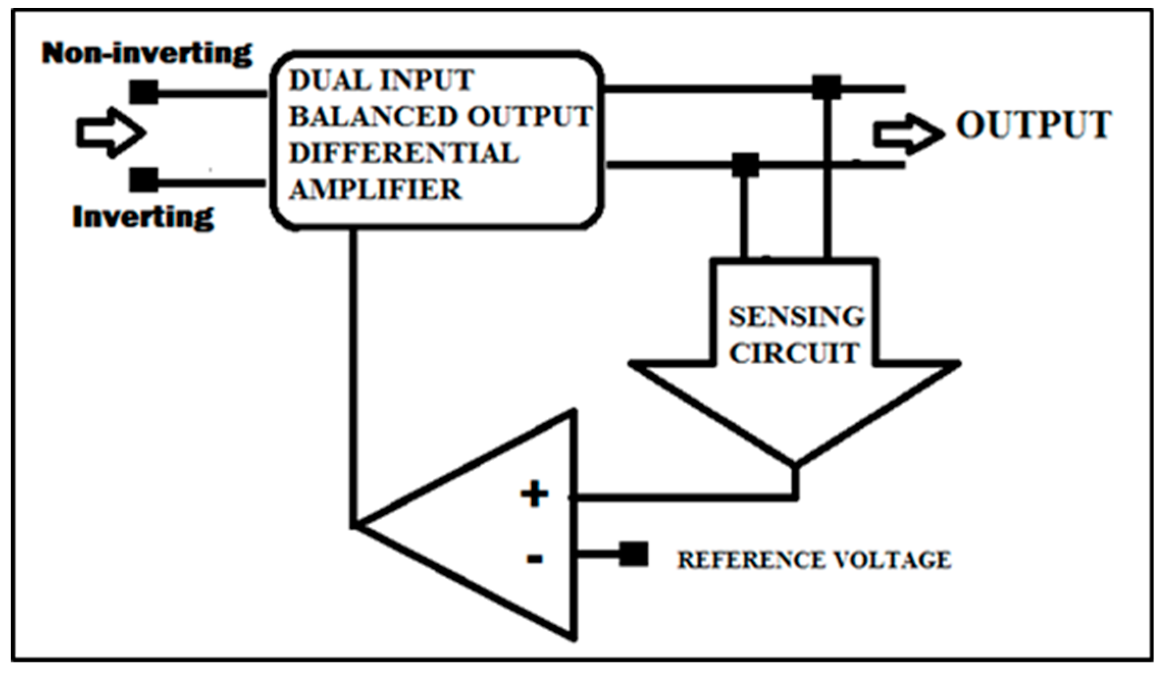
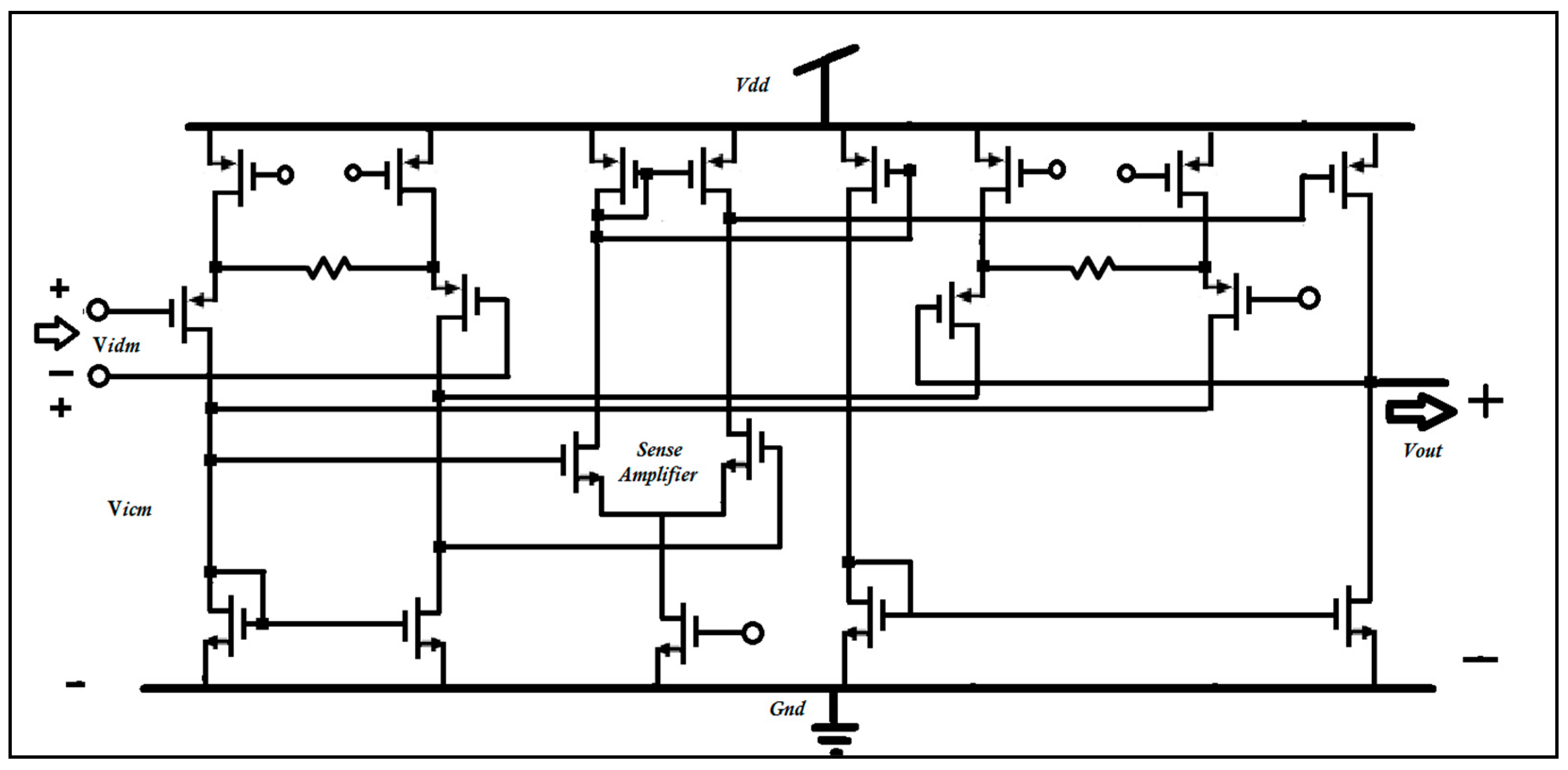
Figure 1 depicts the block architecture for common-mode feedback structure [20]. It incorporates three major blocks. First, there is a fully differential pair amplifier that works in balanced mode. Next, there is a sensing circuit stage which senses common mode output signal. In the final stage, there is a comparator which compares this output common mode signal with a reference voltage and feeds the rectified signal back to the fully differential pair that, in turn, adjusts according to this signal [21]. The reference voltage ideally equals 0 V. Thus, a rectified signal is formed and applied to the fully differential pair, such that, finally, the alteration signal becomes near to zero. The rectified signal is a subtracted value taken by subtracting the reference voltage and the common-mode signal [22,24].
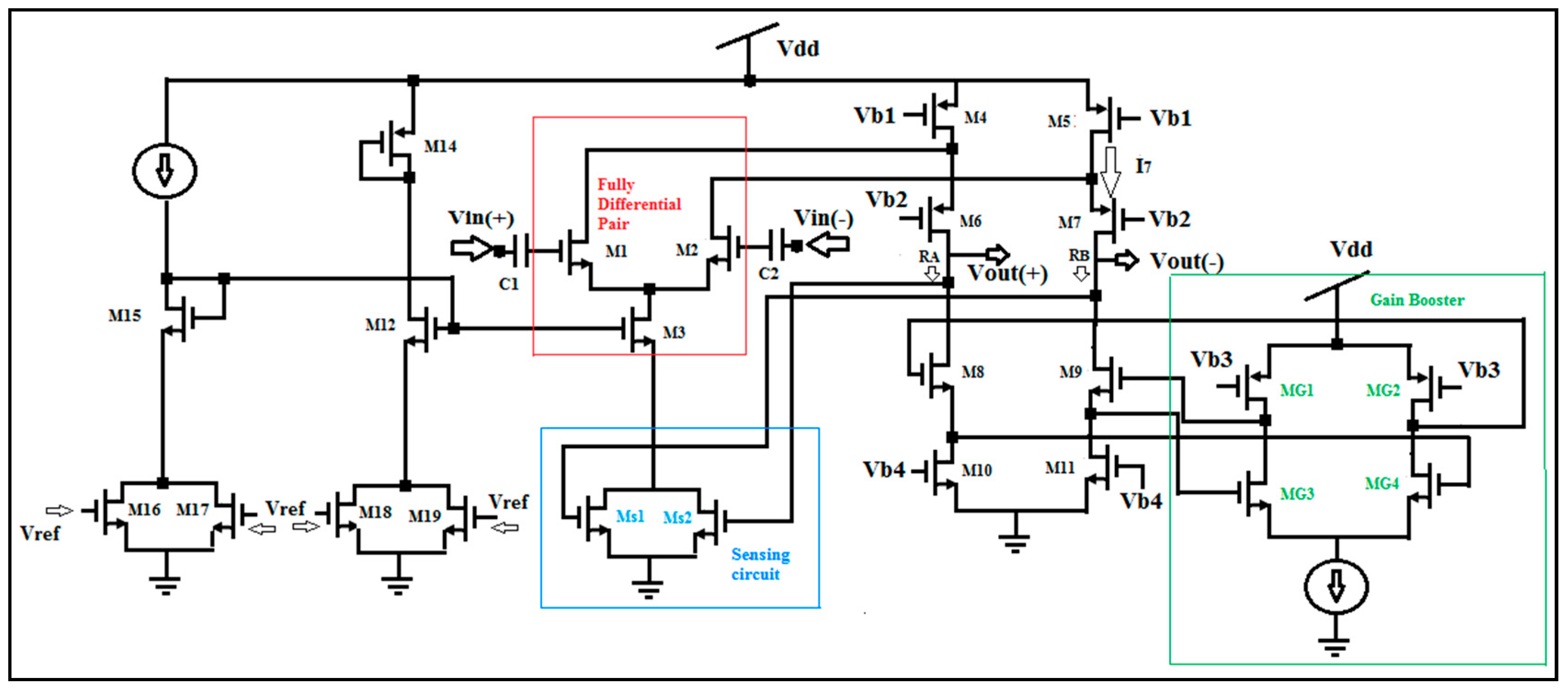
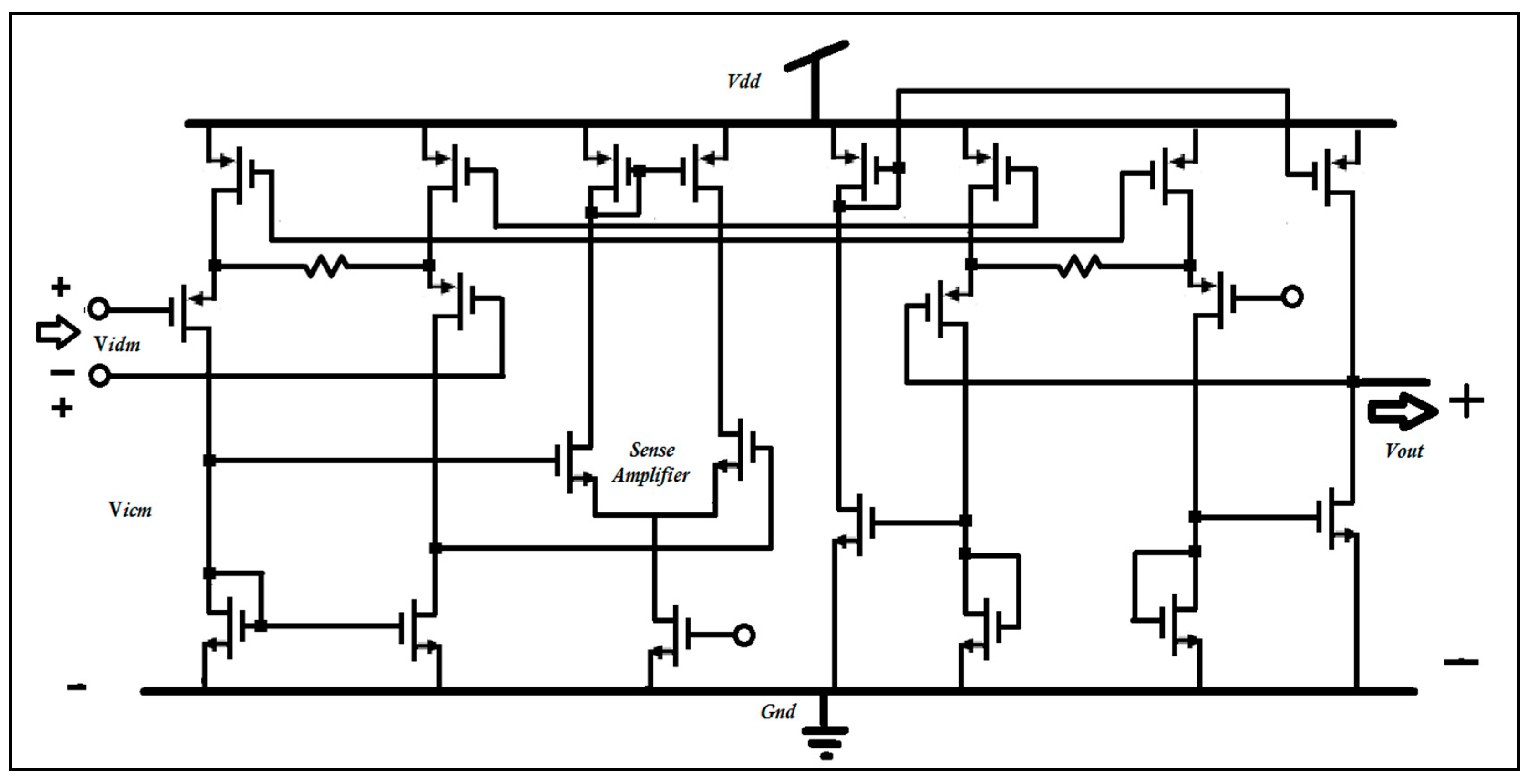
Figure 2 shows the entire architecture of the modified op-amp comparator (GB-CMFD) with gain boosting and common mode current feedback [23,24,25]. Inputs are given to the dual input fully differential pair that comprises of M1 and M2 MOSFETS. The output of this differential pair is taken from the output node which incorporates folded cascode current mirrors as source and sink. M4, M5, M6, and M7 form a current source while, on the other hand, M8, M9, M10, and M11 forms a current sink [26]. The sensing circuit comprises Ms1 and Ms2, which sense the common mode signal from the output node. Next, this signal is compared with the reference voltage through a comparator circuit through M3 and M12.
Further, the correction signal is fed to the fully differential pair through M3 and, thus, it adjusts its operating current according to the correction signal and reduces the common mode gain. A gain booster block which includes MG1, MG2, MG3, and MG4 is also added along with this circuit. This block is responsible for the gain boosting.
The difference signal taken from the differential pair M1 and M2 is amplified further by the next stage, which comprises of eight MOS devices. RA and RB are the output resistances at output nodes vout(+) and vout(−), respectively. These output resistances are responsible for the high output gain of the op-amp comparator circuit as the gain of any amplifier is estimated by the product of its transconductance and output resistance. M8, M9, M10, and M11 MOS devices are arranged and biased in such a manner as to provide high resistance to the output nodes.
In the final segment of the operational amplifier comparator, the gain booster block interacts with the M8 and M9 MOS devices. The output from the drain terminal of M8 and M9 NMOS devices is fed into the gate terminal of MG4 and MG3 MOSFET devices, respectively, which are working in a common source amplifier configuration. The MOS devices MG2 and MG1 are biased with a voltage vb3 and connected to the drain terminal of MG4 and MG3 devices to increase the resistance at the output terminal. Thus, the output of the op-amp comparator gets enhanced by the gain of the gain booster block and is again fed back to the gate terminal of M8 and M9 devices and, thus, the overall output gain of operational amplifier comparator gets boosted.
Major differences in this modified schematic with respect to the general CMFD topology [23,24,25] are the less complicated structure by utilizing fewer MOS devices, which ultimately reduces power consumption of this modified structure. For gain boosting this structure employs only one gain boosting block in the pull-down section. As there are fewer MOS devices in the pull-up section, it results in the fast charging of the output node, which eventually leads to a high slew rate.

Mathematical Analysis

Gain for the differential pair is given as:
G a i n = E f f e c t i v e   g m · E f f e c t i v e   R o u t
where, gm is the effective trans-conductance and Rout is the effective output resistance [1,13]. Looking at the output node Vout the resistance RB can be calculated as given in Equation (1):
R B   = ( r d s 7 + g m 9 · r d s 9 · r d s 11 ) g m 7     r d s 7
R B   = ( r o 7 + g m 9 · r o 9 · r o 11 ) g m 7     r o 7
Additionally, the current I7 that flows through this output node can be calculated as:
I 7 = { g m 2 ( r o 2 r o 5 ) 2   [ ( g m 9   .   r o 9   .   r o 11 g m 7   r o 7 ) + ( r o 2 r o 5 ) ] } . V i n ( )
I 7 = { g m 2   .   V i n ( ) 2   { 1 + [ ( g m 9   .   r o 9   .   r o 11 g m 7   r o 7 ) .   ( g d s 2 + g d s 5 ) ] } }
From Equations (1) and (3) the output voltage gain comes out to be:
V o u t V i n = { g m 1 2 + { g m 2   .   V i n ( ) 2   { 1 + [ ( g m 9   .   r o 9   .   r o 11 g m 7   r o 7 ) .   ( g d s 2 + g d s 5 ) ] } } }   .   R o u t
where Rout is given as:
R o u t = [ g m 9   .   r o 9   .   r o 11 ]     [ g m 7   r o 7 ( r o 2 r o 5 ) ]
Rearranging and solving the Equation (4) by assuming trans-conductance and output resistance of all mirrors as gm and ro:
V o u t V i n = { g m 1 2   .   r o 2 4 }
Now, solving for the gain boosting circuit, Rout can be calculated as:
R o u t = [ A .   g m 9   .   r o 9   .   r o 11 ]     [   g m 7   r o 7 ( r o 2 r o 5 ) ]
Again, solving for gain:
V o u t V i n = { A   .   g m 1 2   .   r o 2 4 }
Comparing Equations (5) and (6) it can be easily concluded that with the modified architecture the gain improves in comparison to the general common feedback structure [23,24,25].

3. Results

In this segment, all the required simulations, such as transient, AC analysis, along with parameter variations of the modified circuit using a closed loop configuration is demonstrated. Monte Carlo simulations have been performed by using SPICE in 90 nm CMOS technology. At least 20 iterations are performed by utilizing the Monte Carlo simulation methods for concluding the final results.
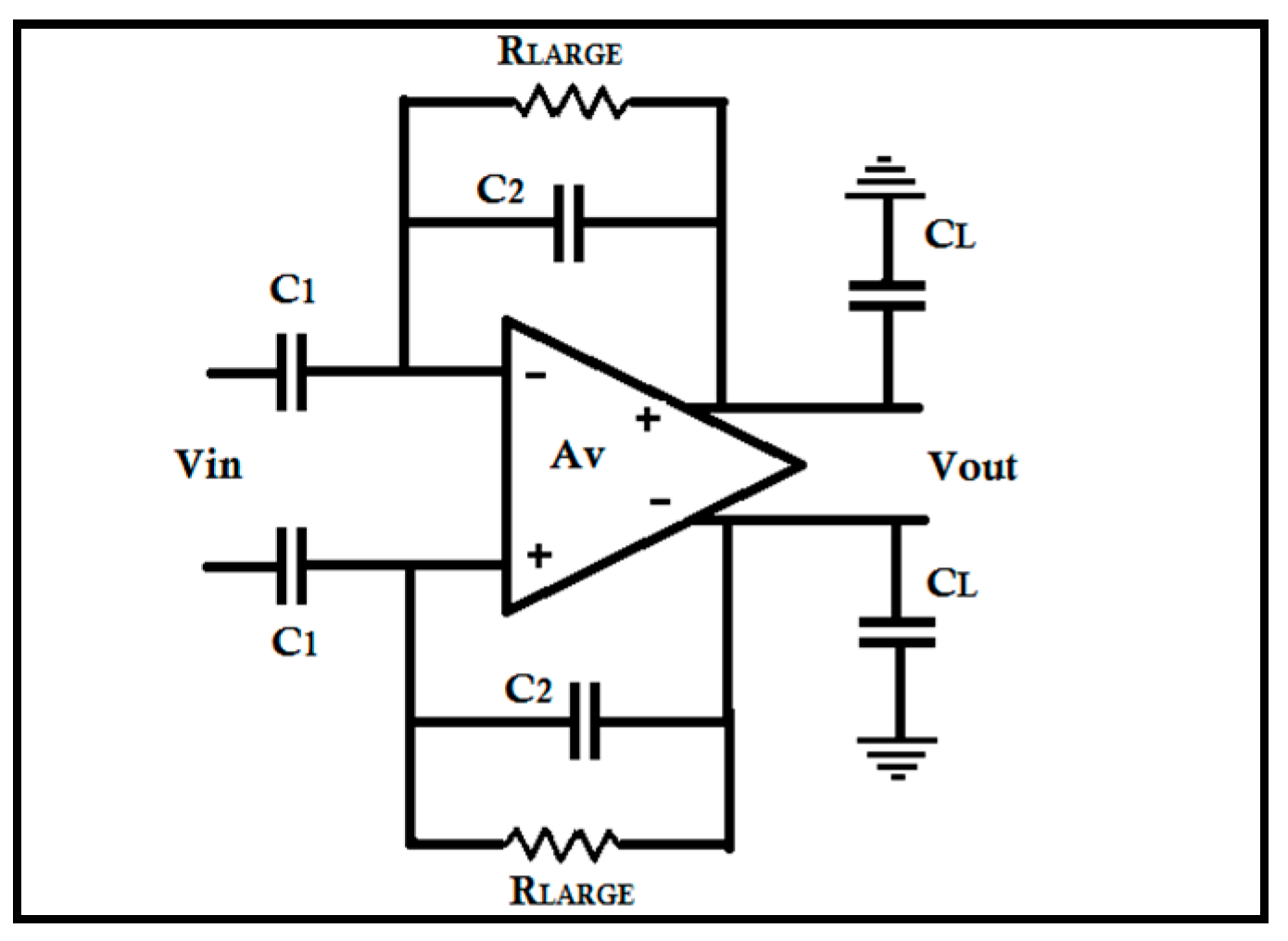
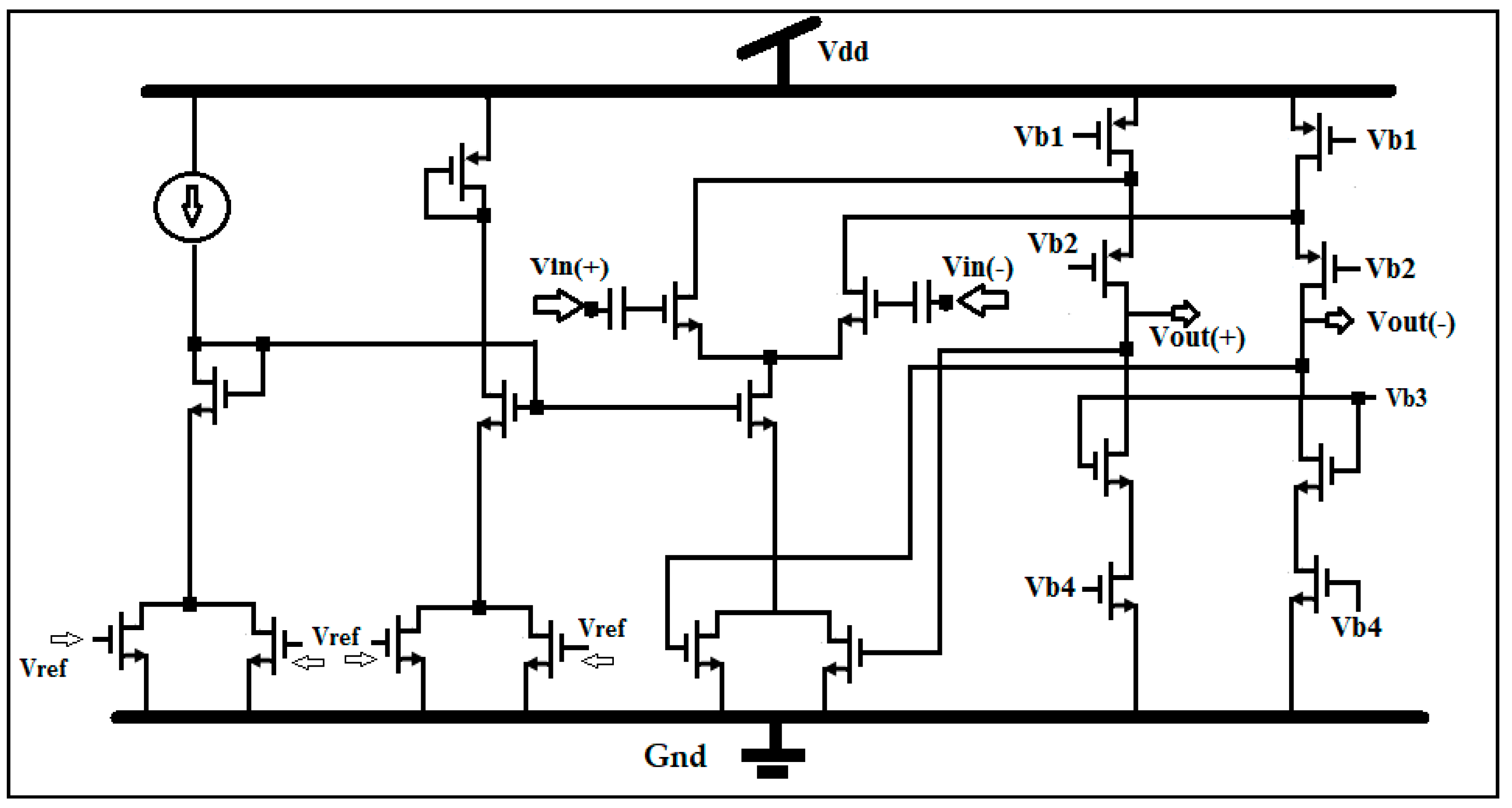
An op-amp with a feedback circuit is designed to have a gain of 20. The design schematic blocks of that are shown in Figure 3 [15,27].
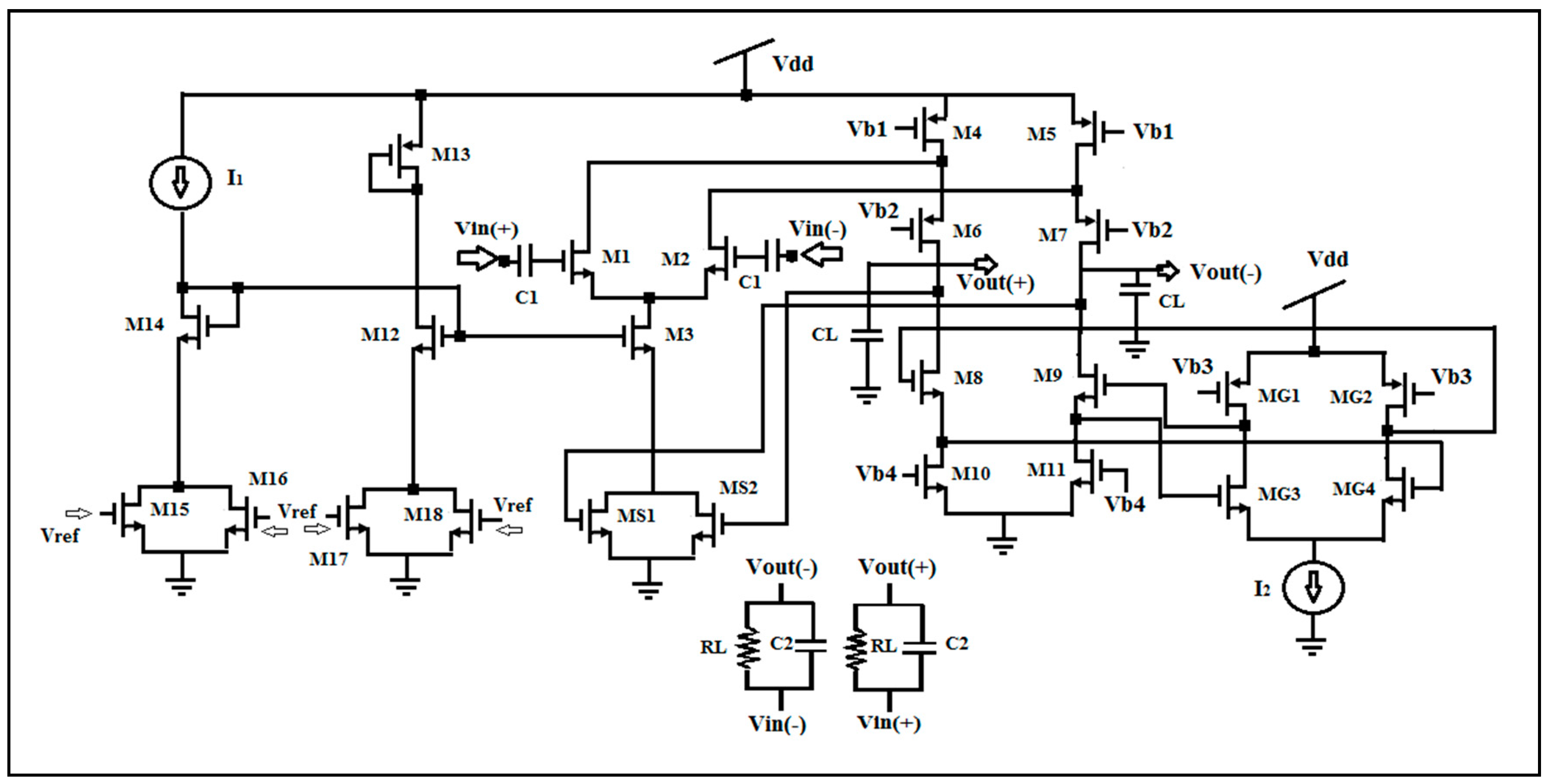
Figure 4 represents the modified circuit of the op-amp comparator employing common mode current feedback with folded cascoded current mirrors along with gain-boosting circuit. The channel length of 90 nm and the channel width of 1 µm is used as the dimension of MOS devices in the proposed op-amp comparator modified architecture.
Table 1 shows the power consumption, maximum current drawn, and the rise time and fall time of the modified op-amp (GB-CMFD) comparator. Simulation is done on a supply voltage of 0.7 V at 25 °C.
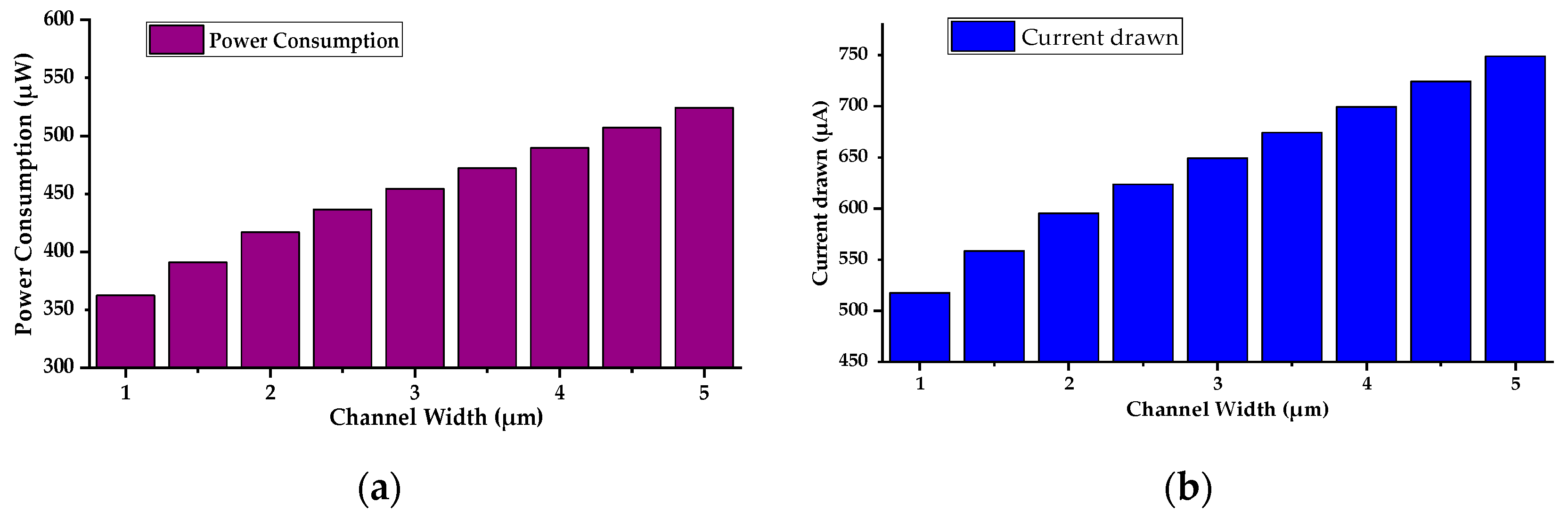
Variations in the parameters when the channel width is varied from 1 µm to 5 µm are also included in Table 1. This circuit draws a maximum current of 517 µA by consuming the power of 362 µW at 1 µm channel width. The values of power consumption and current drawn are increased by 44% when the channel width is increased to 5 µm. Figure 5a,b shows these variations graphically.
Table 1 also gives the details regarding the rising and falling duration for the output pulse and its variation with channel width. Rise and fall times of 7 ps are observed for both rising and falling edges. The variations in these values are negligible with the variation in channel width.
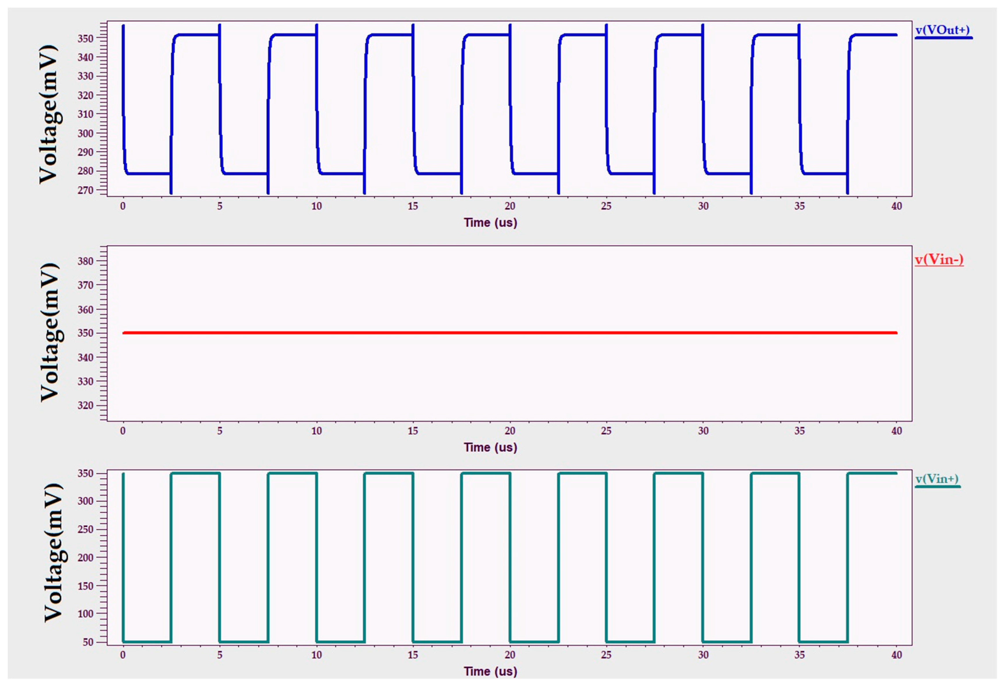
Figure 6 gives details regarding the output waveforms that are recorded with respect to the input waves for the modified structure (CMFD-GB). The input voltage at the negative terminal is kept constant at 350 millivolts and then a varying voltage is applied at the positive terminal. The output waveform at the non-inverting terminal, which is recorded, is shown in Figure 6.
Table 2 shows power consumption, observed closed loop gain, open loop gain, gain error, and slew rate of the modified GB-CMFD comparator. Simulation is done at a supply voltage of 0.7 V by varying the temperature from −5 °C to 55 °C.
In 
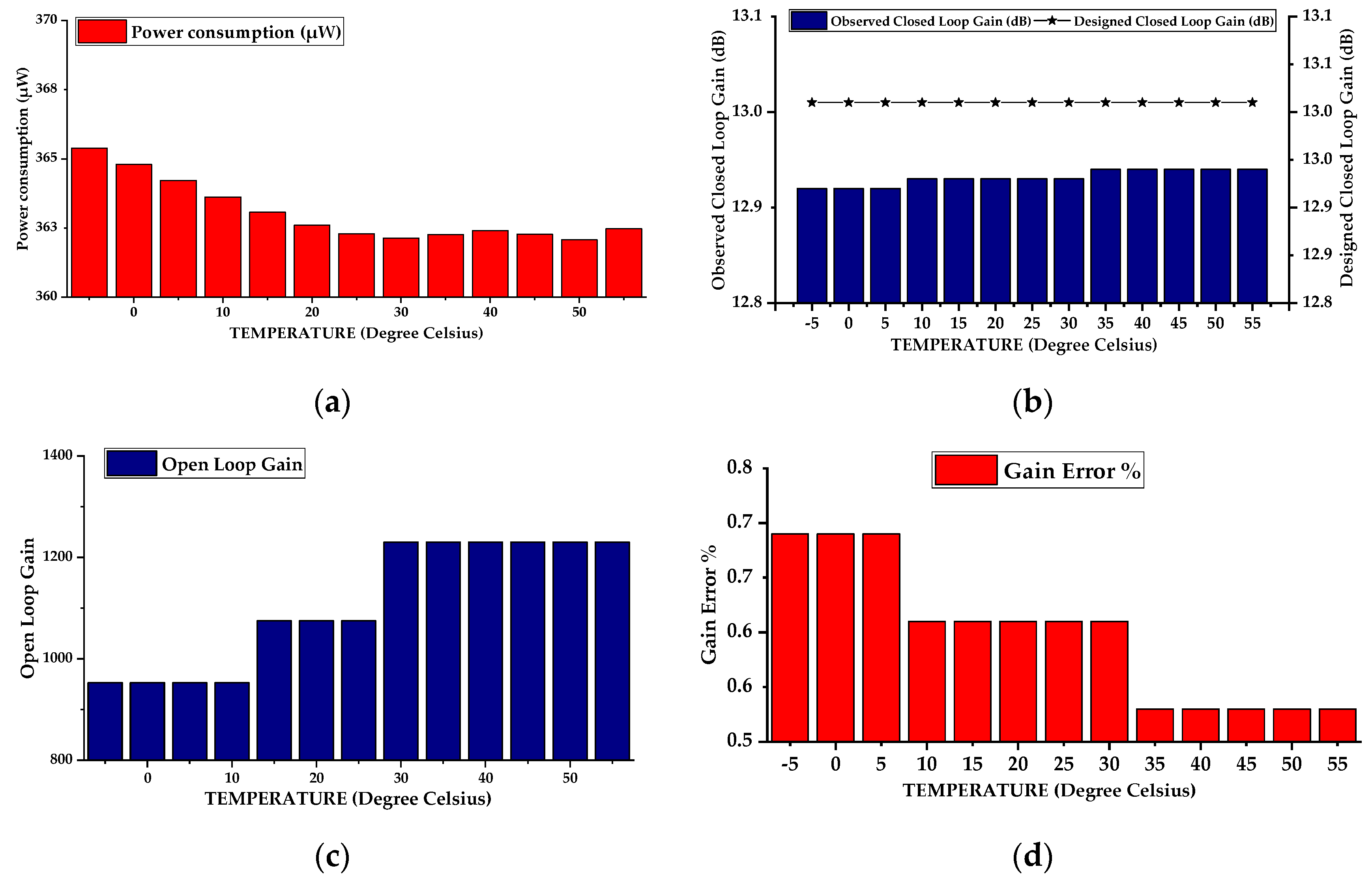
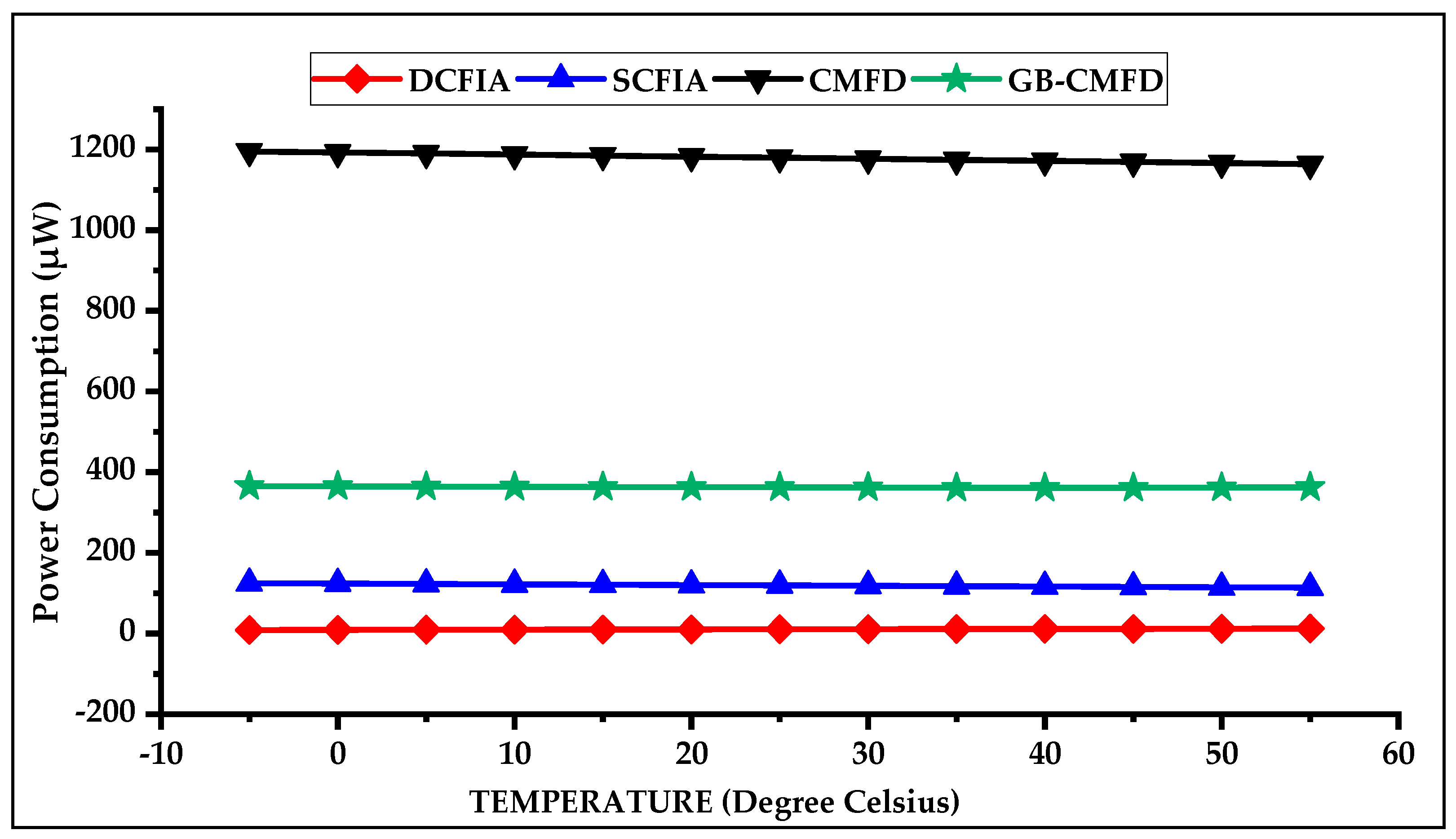
Table 2 the variations in the power consumption are detailed. The modified circuit consumes 362 µW at 25 °C. This value increases marginally but remains close to 362 µW when the temperature is raised to 55 °C. On the other hand, when the temperature was reduced to −5 °C the power consumption increased further and attained the value of 365 µW at −5 °C. Figure 7a shows the variations of power consumption with temperature.
Figure 7b,c exhibit the observed closed loop gain and open loop gain variations with temperature. An observed closed loop gain of 12.93 decibels at 25 °C is recorded, which is very close to the designed closed loop gain of 13.01 decibels. Diminutive level variations are recorded when the temperature varied from −5 to 55 °C. Open loop gain is then detailed with its variations with temperature. The open loop gain of 1075 is observed for the GB-CMFD structure at 25 °C, which is quite large as compared to standard comparator structures. The open loop gain of 1075 is recorded for the modified architecture at 25 °C, which increases to 1229 when the temperature is raised to 55 °C. However, the open loop gain reduced to 953 when the temperature is reduced to −5 °C. Overall, the percentage variations of the open loop gain are 11% to 14% with the variations in temperature.
The gain error variations with temperature are shown in Table 2. Though the circuit is designed in a closed loop configuration for the power gain of 20, which equals 13.01 dB, the values that are obtained from the magnitude plot are marginally different at different temperatures. The gain error is almost constant for the temperature range of −5 to 25 °C and has an error of 0.1% from the expected value, which is relatively acceptable. Figure 7d shows the variations of gain error with temperature.
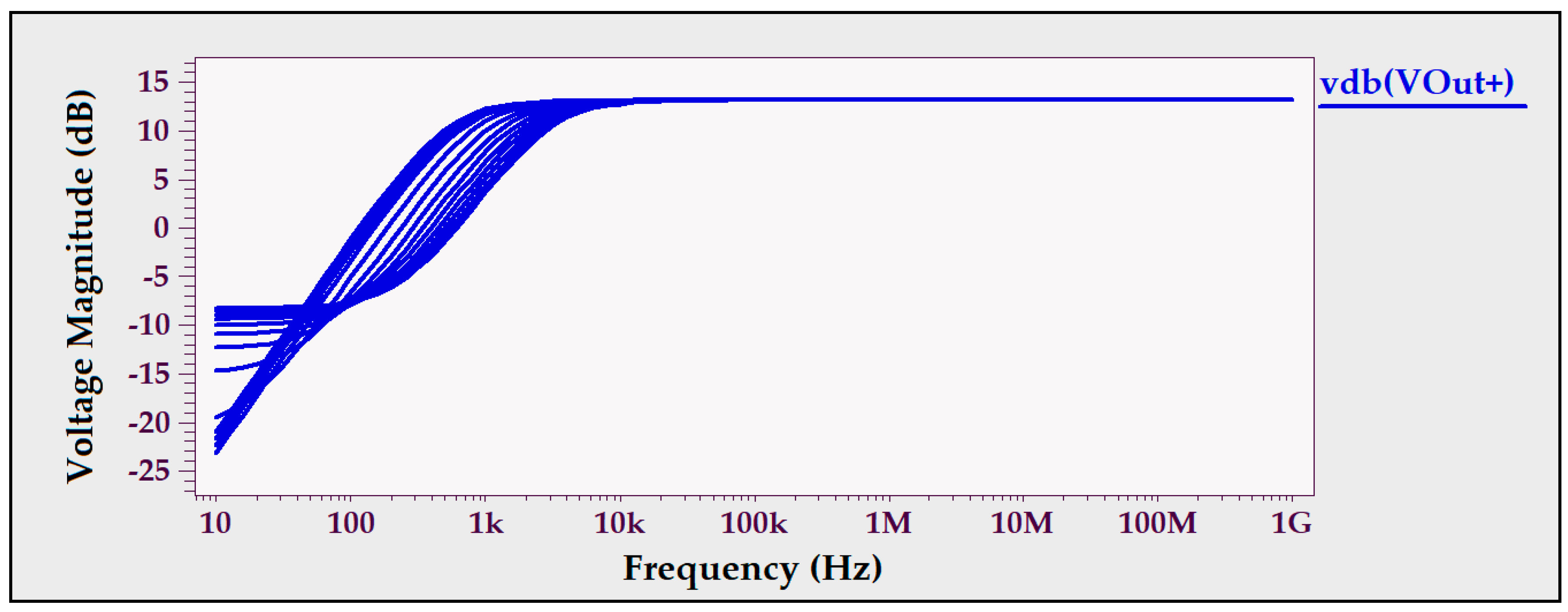
Figure 8 represents the frequency response of the closed loop CMFD-GB structure. The variations in the closed loop gain with respect to temperature can be easily observed from this response.
In the end Table 2 gives the details regarding the slew rate of the modified gain boosting CMFD comparator and its variations with temperature. Slew rate is the measure of the rate at which the output voltage rises with respect to time [28]. Thus, if a comparator has a high slew rate, it will lead to the high speed of comparison [29].
S L E W   R A T E = V O L T A G E   L E V E L   ( V ) R I S E   T I M E   ( µ s )   o r   F A L L   T I M E   ( µ s )
Thus, from the above relation, if a circuit has a very small value of rising time and fall time then it will eventually have a very high slew rate.
From 
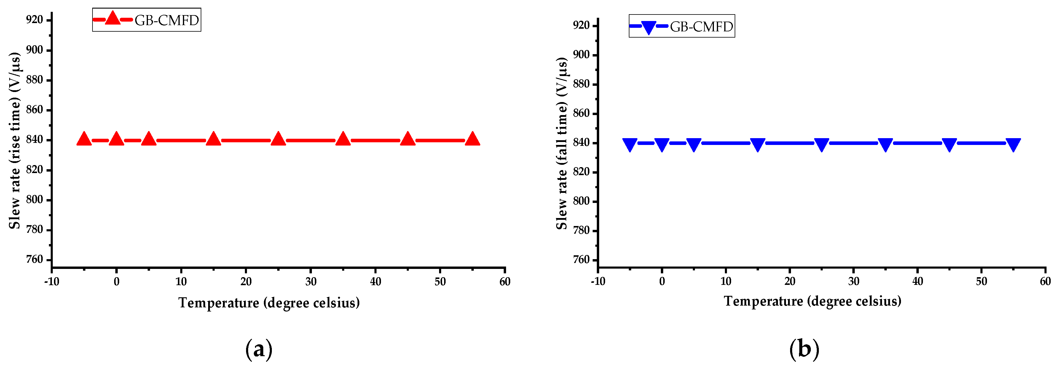
Table 1 the rise time and fall time for this modified GB-CMFD circuit are seven picoseconds and the maximum minus minimum voltage range that is observed after the simulation is 0.006 V for both the rising and falling edge. Thus, using these values, a slew rate of 839 V/µs is obtained for the circuit, which is quite a high value as compared to the other comparators. Figure 9a,b shows the variations of the slew rate for charging and discharging edge with temperature.
It can be seen that this variation is very minute and, thus, this circuit has a high slew rate which is almost stable with temperature variations.
Table 3 summarizes the performance of the modified gain boosting CMFD comparator. CMOS technology is used to design this circuit with the channel length of 90 nm and channel width of 1 µm. A supply voltage of 0.7 V is deployed for the simulations. Twenty-four MOS transistors are used for designing the circuit, along with four capacitors and two resistors. The value of power consumption at 25 °C is 362 µW while drawing a current of 517 µA, both having a variation of approximately 2%. A total of 12.93 decibels of closed loop gain is observed at 25 °C, which is quite close to the calculated gain of 13.01 decibels.
The open loop gain of 1075 is attained by this structure at 25 °C, which is large, compared to normal comparator structures. A gain error of 0.6% is obtained after simulation of this circuit at 25 °C, which is relatively acceptable. A very high slew rate is achieved by this modified design that is 839 V/µs that will eventually lead to a very high speed of comparison and, thus, this comparator can be utilized in designing high-speed analog circuits, such as ADCs and DACs [30,31,32].
Table 4 summarizes the percentage variation of these parameters with temperature. Power consumption varies substantially with the decrease in temperature. A total of 0.07% of marginal variations are recorded for observed closed loop gain, which almost equals zero and is acceptable. Open loop gain variations are then shown in the table, which varies from 12% at −5 °C and 14% at 55 °C. Significant variations in the gain error are recorded when the temperature scales down to −5 °C on the other hand, when the temperature increased to 55 °C the variations are minimal. Almost null variations are observed for the slew rate.

4. Comparison

To evaluate the proposed modified architecture of the op-amp comparator (GB-CMFD) three more structures of the op-amp comparator are utilized for analyses and comparison. These three structures are DCFIA, SCFIA [19], and CMFD [23,24]. The structural design of these three architectures are depicted in Appendix A (Figure A1, Figure A2 and Figure A3). DCFIA and SCFIA are the amplifiers which employ common mode current feedback from drain and source terminals [10]. CMFD is a common mode current feedback with conventional cascode amplifier [23,24].
These three structures are again simulated in 90 nm CMOS technology. Results that are obtained after Monte Carlo simulation are shown in Table 5.
Figure 10 shows the variations in the power consumptions for all four comparators structures when the temperature is varied from −5 to +55 °C. The proposed modified architecture, despite using 24 MOS transistors, consumes power at a moderate level, which is approximately in the range of 360 µW. It also shows marginal variations with temperature variations.
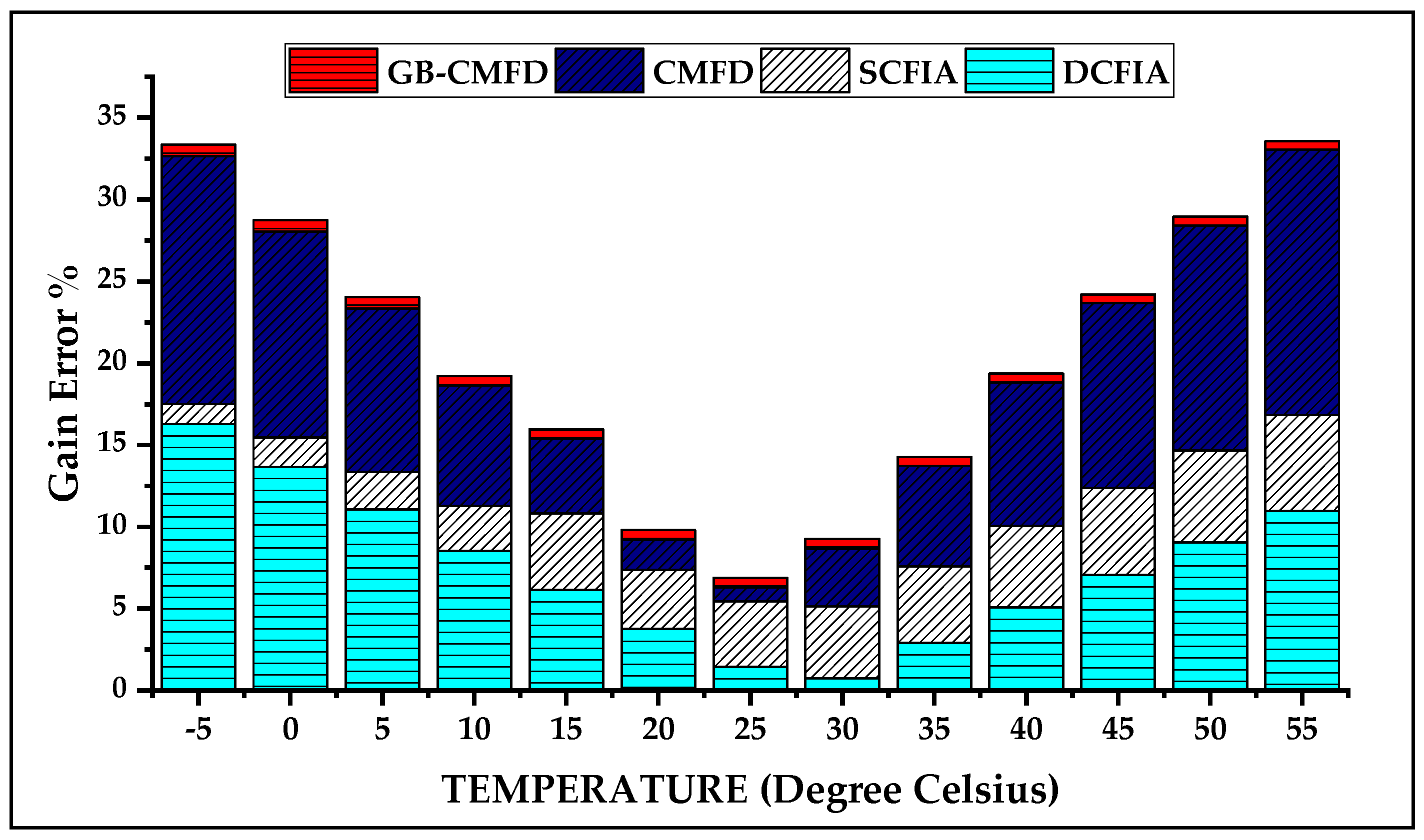
Figure 11 shows the comparison of the gain error value for all four structures. It can be observed from the curves that GB-CMFD has the least value of the percentage gain error. Maximum variations in the gain error is shown by DCFIA and CMFD structures which increased substantially when temperature varies from −5 to +55 °C. SCFIA show the least variation with temperature but has more gain error value than GB-CMFD.
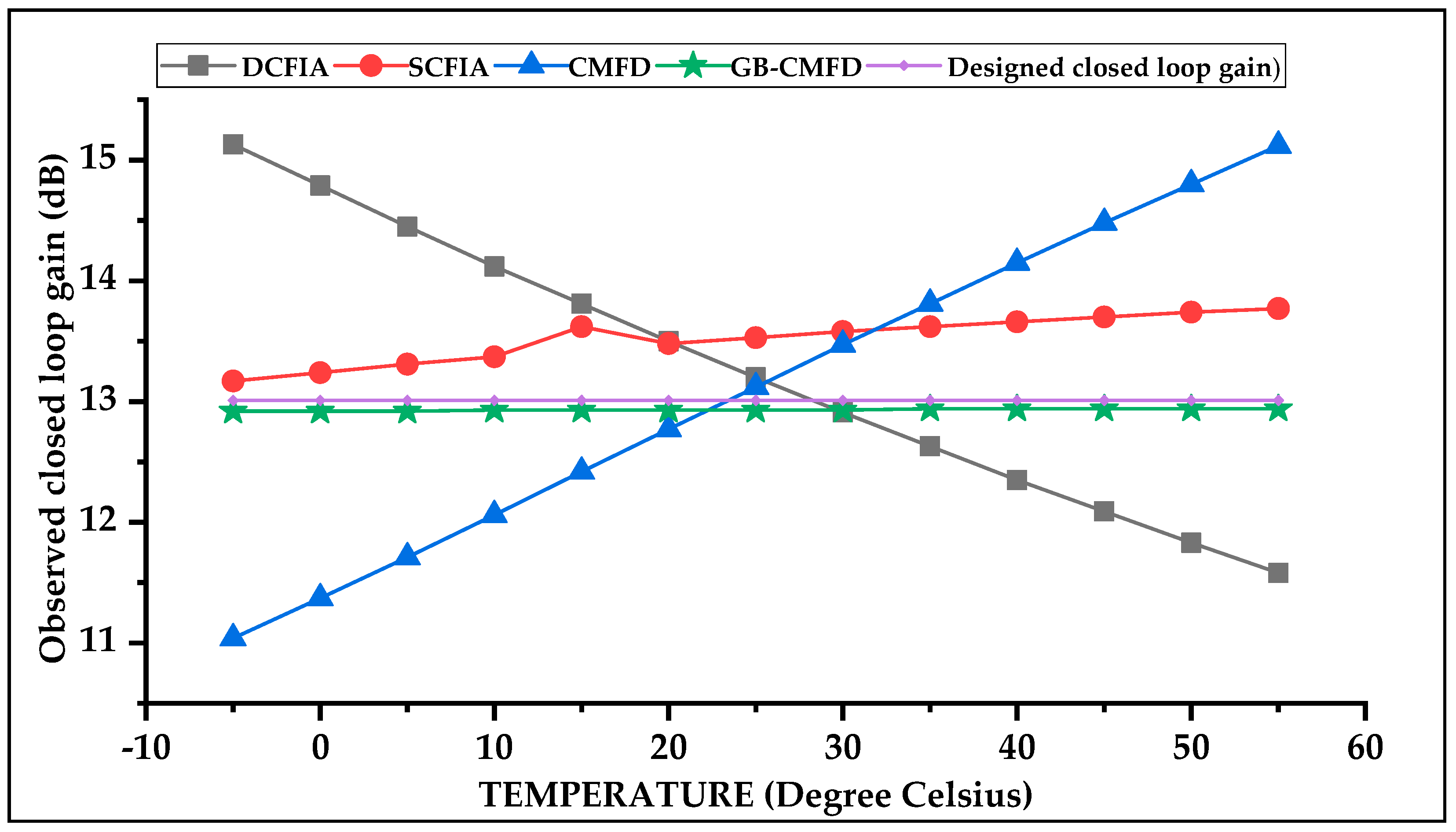
Figure 12 illustrates the variations of observed closed loop gain for all four comparator structures. All four structures are employed in the circuit shown in Figure 3, which is designed for a closed loop gain of 13.01 decibel. The values of actual closed-loop gain that are observed at different temperatures in the simulations are then plotted in Figure 12. The magnitude of the observed closed loop gain for GB-CMFD is almost constant and very close to the designed closed loop value. The magnitude of observed closed loop gain for DCFIA decreases with the increase in temperature opposite to that of the observed CMFD closed loop gain value, which increases with the increase in temperature. The observed SCFIA closed loop gain values are small as compared to DCFIA and CMFD, but substantially large as compared to GB-CMFD.
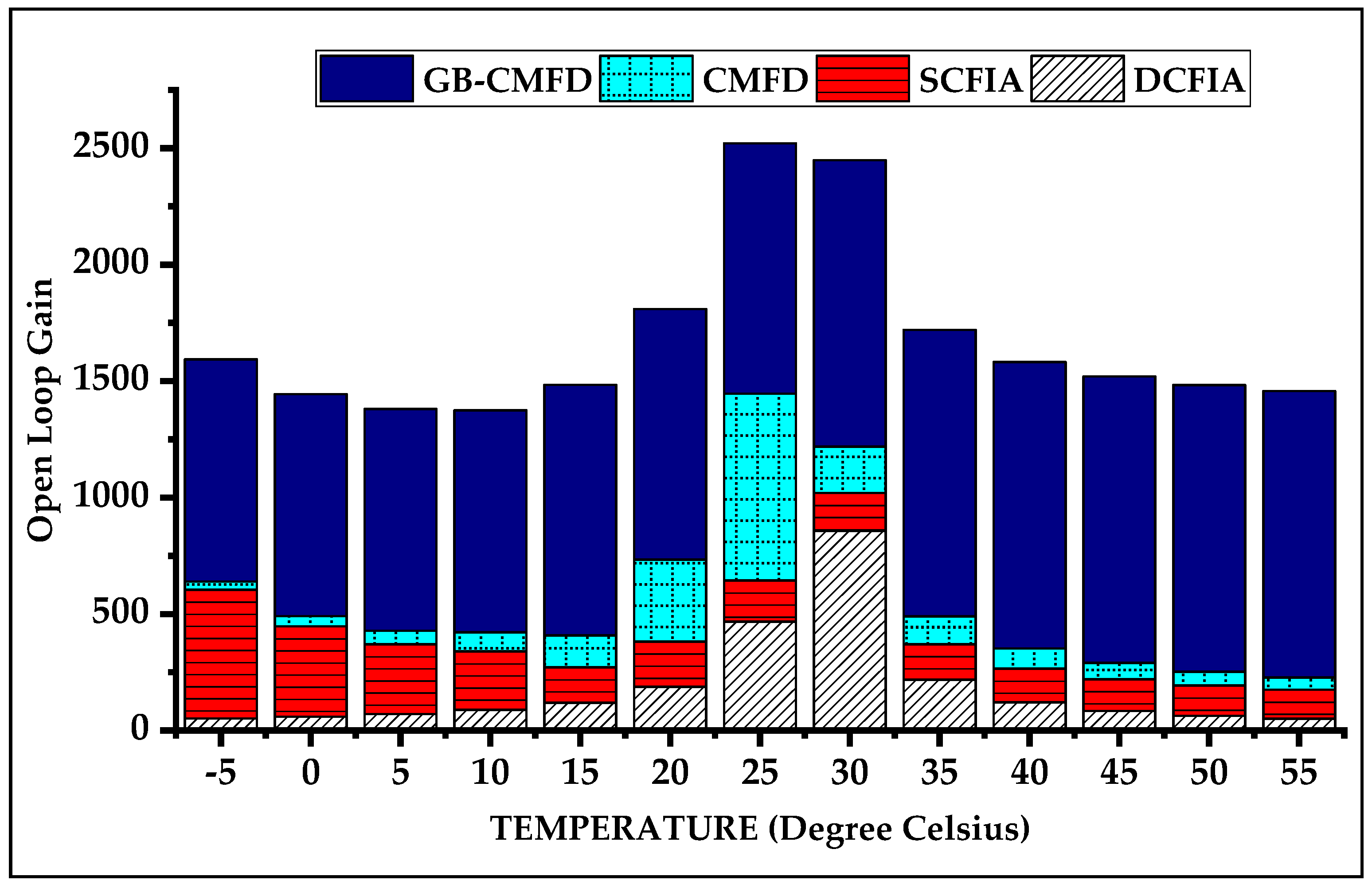
Figure 13 depicts the variations in open loop gain with temperature. The GB-CMFD structure again shows the maximum magnitude of the open loop gain at different temperatures in comparison to other structures.
Table 6 summarizes these parametric variations of all four structures at different temperatures. The modified op-amp comparator (GB-CMFD) shows the least variation in comparison to others in all six parameters which are taken into consideration for comparison.
Table 7 gives details regarding the comparison on the basis of power consumption of this comparator with other pertinent associated studies.

5. Conclusions

A modified architecture of an op-amp comparator to achieve a high slew rate and boosted gain with an improvement in gain design error is proposed and investigated in this manuscript. Deploying the gain booster block and common-mode current feedback structure, the modified architecture of the op-amp comparator (CMFD-GB) achieves an improvement in the overall gain and slew rate with the reduction in gain error and power consumption. An overall gain of 1075 is attained by implementing an additional gain booster block at the end segment of the op-amp comparator that is approximately a 34% improvement as compared to the general common-mode current feedback structure. The rise and fall time also get reduced due to this boosted gain which, in turn, leads to the very high slew rate for this modified op-amp comparator structure. A slew rate of 839 V/µs is observed for this modified op-amp comparator structure, which is quite high and which makes this comparator a prominent contender for high-speed data converters circuits. Closed loop analysis of the modified op-amp comparator structure is done by utilizing this structure for designing a closed feedback amplifier with a gain of 13.01 dB. Results from the simulations depict that the observed and design gain is almost equal for the CMFD-GB comparator with the value of 12.93 decibels. Comparing it to the general CMFD structure, this is an approximately 27% reduction. Considerable reduction in power consumption is also attained through this modified op-amp comparator structure. In spite of using more MOS devices, the power consumption observed for this modified architecture is 362.29 µW, which almost equals a 70% reduction as compared to general CMFD structure. The modified architecture of the op-amp comparator along with high slew rate also shows symmetry for charging and discharging output edges which makes it perfect for the designing of accurate and linear data converter circuits. Temperature sensitivity of these parameters is also observed for the modified comparator architecture by simulating this circuit at different temperatures. The results show an optimum variation of these critical parameters with varying temperature for the modified op-amp comparator architecture (CMFD-GB) as compared to three other architectures. Boosted gain and a large slew rate with optimum power consumption of this modified op-amp comparator structure (CMFD-GB) increases its applicability in high-speed analog and digital circuits, which are designed in ultra deep submicron technologies where high-speed and low-power consumption are the essential design constraints.

Author Contributions

All the authors have contributed to the paper. The designing, writing, and executing the simulations to observe and record the results along with analysis is done by A.K. The work is done under the supervision of M.K. and S.D.

Funding

This research received no external funding.

Conflicts of Interest

The authors declare no conflict of interest.

Abbreviations

GBGain boosting
CMCommon mode
CMFDCommon mode feedback
PCPower consumption
DCFIADrain current feedback instrumentation amplifier
SCFIASource current feedback instrumentation amplifier

Appendix A

Figure A1. Drain current feedback instrumentation amplifier (DCFIA) schematic.
Jlpea 08 00033 g0a1
Figure A2. Source current feedback instrumentation amplifier (SCFIA) schematic.
Jlpea 08 00033 g0a2
Figure A3. Common mode current feedback schematic.
Jlpea 08 00033 g0a3

References

  1. Jendernalik, W. An Ultra-Low-Energy Analog Comparator for A/D Converters in CMOS Image Sensors. Circuits Syst. Signal Process. 2017, 36, 4829–4843. [Google Scholar] [CrossRef] [Green Version]
  2. Ay, S.U. Energy Efficient Supply Boosted Comparator Design. J. Low Power Electron. Appl. 2011, 1, 247–260. [Google Scholar] [CrossRef] [Green Version]
  3. Savani, V.; Devashrayee, N.M. Design and Analysis of Low-Power High-Speed Shared Charge Reset Technique Based Dynamic Latch Comparator. Microelectron. J. 2018, 74, 116–126. [Google Scholar] [CrossRef]
  4. Xin, X.; Cai, J.; Xie, R.; Wang, P. Ultra-Low Power Comparator with Dynamic Offset Cancellation for SAR ADC. Electron. Lett. 2017, 53, 1572–1574. [Google Scholar] [CrossRef]
  5. Bindra, H.S.; Lokin, C.E.; Schinkel, D.; Annema, A.J.; Nauta, B. A 1.2-V Dynamic Bias Latch-Type Comparator in 65-Nm CMOS With 0.4-MV Input Noise. IEEE J. Solid-State Circuits 2018, 53, 1902–1912. [Google Scholar] [CrossRef]
  6. Richelli, A.; Colalongo, L.; Kovacs-Vajna, Z.; Calvetti, G.; Ferrari, D.; Finanzini, M.; Pinetti, S.; Prevosti, E.; Savoldelli, J.; Scarlassara, S. A Survey of Low Voltage and Low Power Amplifier Topologies. J. Low Power Electron. Appl. 2018, 8, 1–20. [Google Scholar] [CrossRef]
  7. Savani, V.; Devashrayee, N.M. Analysis and Design of Low-Voltage Low-Power High-Speed Double Tail Current Dynamic Latch Comparator. Analog Integr. Circuits Signal Process. 2017, 93, 287–298. [Google Scholar] [CrossRef]
  8. Khatak, A.; Dhull, S.; Taleja, M.K. A Study on Advanced High Speed and Ultra Low Power ADC Architectures. Indian J. Sci. Technol. 2017. [Google Scholar] [CrossRef]
  9. Taghizadeh, A.; Koozehkanani, Z.D.; Sobhi, J. A New High-Speed Low-Power and Low-Offset Dynamic Comparator with a Current-Mode Offset Compensation Technique. AEU—Int. J. Electron. Commun. 2017, 81, 163–170. [Google Scholar] [CrossRef]
  10. Bano, S.; Narejo, G.B.; Ali Shah, S.M.U. Power Efficient Fully Differential Bulk Driven OTA for Portable Biomedical Application. Electronics 2018, 7, 41. [Google Scholar] [CrossRef]
  11. Khatak, A.; Kumar, M.; Dhull, S. Analysis of CMOS Comparator in 90nm Technology with Different Power Reduction Techniques. Int. J. Electr. Comput. Eng. 2018, 8. [Google Scholar] [CrossRef]
  12. Zahrai, S.A.; Onabajo, M. Review of Analog-To-Digital Conversion Characteristics and Design Considerations for the Creation of Power-Efficient Hybrid Data Converters. J. Low Power Electron. Appl. 2018, 8, 12. [Google Scholar] [CrossRef]
  13. Dubey, A.K.; Nagaria, R.K. Optimization for Offset and Kickback-Noise in Novel CMOS Double-Tail Dynamic Comparator: A Low-Power, High-Speed Design Approach Using Bulk-Driven Load. Microelectron. J. 2018, 78, 1–10. [Google Scholar] [CrossRef]
  14. Khorami, A.; Sharifkhani, M. A Low-Power High-Speed Comparator for Precise Applications. IEEE Trans. Very Large Scale Integr. (VLSI) Syst。 2018, 1–12. [Google Scholar] [CrossRef]
  15. Kumaravel, S.; Venkataramani, B. An Improved Recycling Folded Cascode OTA with Positive Feedback. WSEAS Trans. Circuits Syst. 2014, 13, 85–93. [Google Scholar]
  16. Ragheb, A.N.; Kim, H.W. Ultra-Low Power OTA Based on Bias Recycling and Subthreshold Operation with Phase Margin Enhancement. Microelectron. J. 2017, 60, 94–101. [Google Scholar] [CrossRef]
  17. Maloberti, F.; Pea-Perez, A.; Gonzalez-Diaz, V.R. Opamp Gain Compensation Technique for Continuous-Time ΣΔ Modulators. Electron. Lett. 2014, 50, 355–356. [Google Scholar]
  18. Khorami, A.; Sharifkhani, M. Excess Power Elimination in High-Resolution Dynamic Comparators. Microelectron. J. 2017, 64, 45–52. [Google Scholar] [CrossRef]
  19. Worapishet, A.; Demosthenous, A. Generalized Analysis of Random Common-Mode Rejection Performance of CMOS Current Feedback Instrumentation Amplifiers. IEEE Trans. Circuits Syst. I Regul. Pap. 2015, 62, 2137–2146. [Google Scholar] [CrossRef]
  20. Lee, J.Y.; Hwang, S.N. A High-Gain Boost Converter Using Voltage-Stacking Cell. Trans. Korean Inst. Electr. Eng. 2008, 57, 982–984. [Google Scholar]
  21. Ng, K.A.; Xu, Y.P. A Low-Power, High CMRR Neural Amplifier System Employing CMOS Inverter-Based OTAs With CMFB Through Supply Rails. IEEE J. Solid-State Circuits 2016, 51, 724–737. [Google Scholar]
  22. Mahdavi, S.; Noruzpur, F.; Ghadimi, E.; Khanshan, T.M. A New Fast Rail-to-Rail Continuous-Time Common-Mode Feedback Circuit. In Proceedings of the 2017 MIXDES—24th International Conference Mixed Design of Integrated Circuits and Systems, Bydgoszcz, Poland, 22–24 June 2017; pp. 387–391. [Google Scholar]
  23. Haga, Y.; Zare-Hoseini, H.; Berkovi, L.; Kale, I. Design of a 0.8 Volt Fully Differential CMOS OTA Using the Bulk-Driven Technique. In Proceedings of the 2005 IEEE International Symposium on Circuits and Systems, Kobe, Japan, 23–26 May 2005; pp. 220–223. [Google Scholar]
  24. Duque-Carrillo, J.F. Control of the Common-Mode Component in CMOS Continuous-Time Fully Differential Signal Processing. Analog Integr. Circuits Signal Process. 1993, 4, 131–140. [Google Scholar] [CrossRef]
  25. Bult, K.; Geelen, G.J.G.M. The CMOS Gain-Boosting Technique. Analog Integr. Circuits Signal Process. 1991, 1, 119–135. [Google Scholar] [CrossRef]
  26. Hassanpourghadi, M.; Zamani, M.; Sharifkhani, M. A Low-Power Low-Offset Dynamic Comparator for Analog to Digital Converters. Microelectron. J. 2014, 45, 256–262. [Google Scholar] [CrossRef]
  27. Zhao, X.; Zhang, Q.; Wang, Y.; Deng, M. Transconductance and Slew Rate Improvement Technique for Current Recycling Folded Cascode Amplifier. AEU—Int. J. Electron. Commun. 2016, 70, 326–330. [Google Scholar] [CrossRef]
  28. Aggarwal, B.; Gupta, M.; Gupta, A.K. A Comparative Study of Various Current Mirror Configurations: Topologies and Characteristics. Microelectron. J. 2016, 53, 134–155. [Google Scholar] [CrossRef]
  29. Danesh, S.; Hurwitz, J.; Findlater, K.; Renshaw, D.; Henderson, R. A Reconfigurable 1 GSps to 250 MSps, 7-Bit to 9-Bit Highly Time-Interleaved Counter ADC with Low Power Comparator Design. IEEE J. Solid-State Circuits 2013, 48, 733–748. [Google Scholar] [CrossRef]
  30. Miki, T.; Morie, T.; Matsukawa, K.; Bando, Y.; Okumoto, T.; Obata, K.; Sakiyama, S.; Dosho, S. A 4.2 MW 50 MS/s 13 Bit CMOS SAR ADC With SNR and SFDR Enhancement Techniques. IEEE J. Solid-State Circuits 2015, 50, 1372–1381. [Google Scholar] [CrossRef]
  31. Maji, K.B.; Kar, R.; Mandal, D.; Ghoshal, S.P. An Evolutionary Approach Based Design Automation of Low Power CMOS Two-Stage Comparator and Folded Cascode OTA. AEU—Int. J. Electron. Commun. 2016, 70, 398–408. [Google Scholar] [CrossRef]
  32. Gupta, R.; Gupta, R.; Sharma, S. Design of High Speed and Low Power 4-Bit Comparator Using FGMOS. AEU—Int. J. Electron. Commun. 2017, 76, 125–131. [Google Scholar] [CrossRef]
  33. Khorami, A.; Sharifkhani, M. High-Speed Low-Power Comparator for Analog to Digital Converters. AEU—Int. J. Electron. Commun. 2016, 70, 886–894. [Google Scholar] [CrossRef]
  34. De La Fuente-Cortes, G.; Espinosa Flores-Verdad, G.; Gonzalez-Diaz, V.R.; Diaz-Mendez, A. A New CMOS Comparator Robust to Process and Temperature Variations for SAR ADC Converters. Analog Integr. Circuits Signal Process. 2017, 90, 301–308. [Google Scholar] [CrossRef]
  35. Goll, B.; Zimmermann, H. A Comparator with Reduced Delay Time in 65-Nm CMOS for Supply Voltages down to 0.65 V. IEEE Trans. Circuits Syst. II Express Briefs 2009, 56, 810–814. [Google Scholar] [CrossRef]
  36. Chua, C.; Kumar, R.B.N.; Sireesha, B. Design and Analysis of Low-Power and Area Efficient N-Bit Parallel Binary Comparator. Analog Integr. Circuits Signal Process. 2017, 92, 225–231. [Google Scholar] [CrossRef]
  37. Rahmani, S.; Ghaznavi-Ghoushchi, M.B. Design and Analysis of a High Speed Double-Tail Comparator with Isomorphic Latch-Preamplifier Pairs and Tail Bootstrapping. Analog Integr. Circuits Signal Process. 2017, 93, 507–521. [Google Scholar] [CrossRef]
Figure 1. Block structure of current mode feedback op-amp.
Jlpea 08 00033 g001
Figure 2. Modified GB-CMFD comparator circuit.
Jlpea 08 00033 g002
Figure 3. An operational amplifier with feedback.
Jlpea 08 00033 g003
Figure 4. Comparator with modified gain boosting current feedback.
Jlpea 08 00033 g004
Figure 5. (a) Power consumption vs. channel width; and (b) current drawn vs. channel width.
Jlpea 08 00033 g005
Figure 6. Output waveforms of CMFD-gain boosting comparator (transient analysis).
Jlpea 08 00033 g006
Figure 7. (a) Power consumption vs. temperature; (b) observed closed loop gain vs. temperature; (c) open loop gain vs. temperature; and (d) gain error vs. temperature.
Jlpea 08 00033 g007
Figure 8. Variations in closed loop gain with temperature (AC analysis).
Jlpea 08 00033 g008
Figure 9. (a) Slew rate (rising edge) vs. temperature; and (b) slew rate (falling edge) vs. temperature.
Jlpea 08 00033 g009
Figure 10. Power consumption vs. temperature.
Jlpea 08 00033 g010
Figure 11. Gain error (%) vs. temperature.
Jlpea 08 00033 g011
Figure 12. Observed closed loop gain vs. temperature.
Jlpea 08 00033 g012
Figure 13. Open loop gain vs. temperature.
Jlpea 08 00033 g013
Table 1. Power consumption, current drawn, and rise and fall times of the modified GB-CMFD.
Supply Voltage = 0.7 VTemp = 25 °C
Width (µm)Power Consumption (µW)Current Drawn (µA)Rise Time (ps)Fall Time (ps)
1.036251777
1.539055877
2.041659577
2.543662377
3.045464977
3.547267477
4.048969977
4.550672477
5.052474877
Table 2. Power consumption, gain error, slew rate, and closed and open loop gain of the modified GB-CMFD at different temperatures.
Temp (°C)Power Consumption (µW)Observed Closed Loop Gain (dB)Open Loop GainGain Error %Slew Rate (Rise Time) (V/µs)Slew Rate (Fall Time) (V/µs)
−5365139530.69839839
0364139530.69839839
5364139530.69839839
153631310750.61839839
253621310750.61839839
353611312290.53839839
453611312290.53839839
553621312290.53839839
Table 3. Comparison of results at 25 °C.
Temperature25 °C
TechnologyCMOS
No. Of Mosfets24
Channel Length90 nm
Channel Width1 µm
Supply voltage0.7 V
Power consumption362 µW
Current drawn517 µA
Observed closed loop gain13 decibels
Gain error %0.6
Open loop gain1075
Slew rate839 V/µs
Table 4. Percentage variation with temperature.
Temperature−5 °C to +55 °C
Power consumption≅0%
Observed closed loop gain≅0%
Open loop gain12% to 14%
Gain error12% to 0.07%
Slew rate≅0%
Table 5. Comparison of simulations results at 25 °C.
DCFIA [19]SCFIA [19]CMFD [23,24]GB-CMFD (Proposed Modified Architecture)
TechnologyCMOSCMOSCMOSCMOS
No. Of Mosfets19212024
Channel Length90 nm90 nm90 nm90 nm
Channel Width1 µm1 µm1 µm1 µm
Supply voltage0.8 V0.8 V1.8 V0.7 V
Power consumption10 µW119 µW1179 µW362 µW
Observed closed loop gain(dB)13.213.513.113
Gain error %130.80.6
Open loop gain4671778011075
Slew rate1 V/µs1 V/µs307 V/µs839 V/µs
Table 6. Percentage variations in parameters when the temperature changes from −5 to 55 °C.
ParametersDCFIA [19]SCFIA [19]CMFD [23,24]GB-CMFD (Proposed Modified Architecture)
Power consumption23 to 164 to 5≅3≅0
Observed closed loop gain15 to 123 to 216 to 15≅0
Open loop gain88 to 89212 to 3096 to 9411 to 14
Gain error16 to 111 to 615 to 1612 to 0.07
Slew rate (charging)≅0≅01 to 6≅0
Slew rate (discharging)≅1≅129 to 27≅0
Table 7. Comparison with other associated studies.
Technology CMOSSupply VoltageSlew RateChannel LengthPower Consumption
[29]350 nm2.5 V161 V/µs350 nm456 µW
350 nm2.5 V176 V/µs350 nm195 µW
[32]130 nm1.0 V 130 nm100 µW
[33]180 nm1.1 V--180 nm1300 µW
[34]180 nm----180 nm≅750 µW
[35]65 nm1.2 V--65 nm2800 µW
[36]65 nm1.2 V 65 nm370 µW
[37]180 nm0.7 V to 1.1 V 180 nm420 µW
GB-CMFD (Proposed-architecture)90 nm0.7 V839 V/µs90 nm362 µW

