Physical Simulations of High Speed and Low Power NanoMagnet Logic Circuits


Department of Electronics and Telecommunications, Politecnico di Torino, Corso Duca Degli Abruzzi 24, 10129 Torino, Italy
*
Author to whom correspondence should be addressed.
J. Low Power Electron. Appl. 2018, 8(4), 37; https://0-doi-org.brum.beds.ac.uk/10.3390/jlpea8040037
Submission received: 29 June 2018
/
Revised: 1 October 2018
/
Accepted: 1 October 2018
/
Published: 8 October 2018
(This article belongs to the Special Issue Quantum-Dot Cellular Automata (QCA) and Low Power Application)
Abstract
:Among all “beyond CMOS” solutions currently under investigation, nanomagnetic logic (NML) technology is considered to be one of the most promising. In this technology, nanoscale magnets are rectangularly shaped and are characterized by the intrinsic capability of enabling logic and memory functions in the same device. The design of logic architectures is accomplished by the use of a clocking mechanism that is needed to properly propagate information. Previous works demonstrated that the magneto-elastic effect can be exploited to implement the clocking mechanism by altering the magnetization of magnets. With this paper, we present a novel clocking mechanism enabling the independent control of each single nanodevice exploiting the magneto-elastic effect and enabling high-speed NML circuits. We prove the effectiveness of this approach by performing several micromagnetic simulations. We characterized a chain of nanomagnets in different conditions (e.g., different distance among cells, different electrical fields, and different magnet geometries). This solution improves NML, the reliability of circuits, the fabrication process, and the operating frequency of circuits while keeping the energy consumption at an extremely low level.
1. Introduction
The high power consumption due to leakage currents and the technological limits of lithography-based techniques used during the fabrication process are making the development of CMOS technology increasingly difficult [1,2]. The scenario of possible substitutive technologies is becoming wider. Among all candidates, nanomagnetic logic (NML) seems to be very promising. This technology is based on the field-coupled nanocomputing paradigm: information propagates according to the magnetic interaction among devices. Devices are characterized by their intrinsic capability to store binary information according to their magnetization state. As depicted in Figure 1A, in NML, logic information can be stored by encoding it into the two possible stable magnetic states. Circuits are designed by placing nanomagnets in a chain fashion, obtaining wires able to transport information. An example is given in Figure 1B.
In fabricated circuits, process variations and thermal noise cause errors in the propagation of the information in long chains of nanodevices: the magnetic field generated by each cell is not sufficient to properly switch other devices without external help [3,4]. This proves the need for a clocking mechanism. Magnets must be forced into an intermediate stable state so that they can properly switch according to neighbor elements. Due to the effect of thermal noise, magnets tend not to maintain their intermediate state. Therefore, the number of magnets that can be cascaded is limited. This maximum number depends on the geometry of the magnet, the energy barrier, and other parameters. In order to correctly propagate logic states, no more than four or five nanomagnets (with dimensions of 50 nm × 100 nm) can be cascaded, as demonstrated in [3]. To overcome this limitation, a clocking mechanism (Figure 1C,D) must be introduced [5,6]. The circuit is divided into different areas called clock zones, composed of only a limited amount of magnets. Multiple clock signals are used to drive the zones. A three-phase clock scheme is employed in Figure 1C. Each clock signal is applied to magnets belonging to a different clock zone (Figure 1D). As a consequence, magnets in the switch state are influenced by neighbor elements that are in a stable state. At the same time, magnets that are in the reset state have no influence on the signal propagation. Figure 1D describes an example of signal propagation, while Figure 1F depicts an example of circuits (a half adder) highlighting the layout of the clock zones, which are represented with different colored stripes. Different mechanisms can be used to control the magnets and to force them in the intermediate (reset) state.
Since NML is intended to work at room temperature, the presence of thermal noise limits the true potential of the technology. The thermal fluctuations of the magnetization, when the magnets are forced in the reset state, can cause unwanted switching and therefore errors during the signal propagation. To increase the reliability of these circuits, an adiabatic switching must be applied. Instead of abruptly forcing the magnets in the reset state, they are switched very slowly. Furthermore, given that a clock zone is composed of many magnets, the length of the clock period must consider the time required for all magnets to switch. The combination of these two effects leads to a clock frequency that is quite low (around 10–30 MHz), limiting the potential of the technology.
In this paper, we adopt a novel technique that makes use of multiple smaller clock zones, overcoming this problem and offering several advantages with respect to traditional approaches [7]. We propose a clock technique that allows the creation of clock zones composed of only one magnet, greatly improving the clock frequency as a result.
The idea is based on the experimental work presented in [7], where a magnet’s magnetization is altered through a mechanical stress which is the consequence of the magneto-elastic effect. It represents an evolution of the idea that we originally proposed in [8], but the physical structure of the clock system is different as it permits each magnet to be controlled independently. It allows the operating frequency of NML circuits to be greatly increased, simultaneously reducing the influence of thermal noise.
A background on the different NML implementations will be given in Section 2. Then, after discussing the physical layout of circuits (Section 3), we present our results by validating them through micromagnetic simulations (Section 4) and by analyzing the energy consumption (Section 4.3). To the best of our knowledge, no complete micromagnetic simulations of NML circuits based on the magneto-elastic effect have yet been presented in literature—only models based on the single-domain approximation of the LLG equation. Therefore, this paper represents a novelty in the literature. The simulations are performed by using MAGPAR [9], a finite element simulator that natively supports the magneto-elastic effect. The behavior of basic structures is validated throughout physical simulations. We also perform a characterization of these structures. In particular, we investigate the impact of the distance among magnets and the impact of different aspect ratios of the magnets on the behavior of circuits. Both of these quantities are directly related to the reliability and the speed of circuits. Increasing the distance among magnets makes the fabrication process easier, because a lower-resolution lithography can be used. However, what is the effect on the circuit behavior and speed? Similarly, increasing the aspect ratio of magnets reduces the effect of process variations, but how does it affect the circuit behavior? We provide an answer to these questions in this paper. We demonstrate that not only can the distance among magnets and their aspect ratio be increased, but the clock frequency that can be obtained is far higher than in normal NML circuits. Overall, the solution that we propose in this paper has three main advantages: it improves the operating speed of NML circuits, it reduces the influence of thermal noise during the switching process, and it simplifies the fabrication process.
2. NML Implementations and Background
The working principle behind nanomagnetic logic (NML) [10] is based on the interaction among neighboring cells through a magnetostatic field. Different physical implementations of this technology have been studied in recent years [11]. Among them, the most relevant are: in-plane NML (iNML), magneto-tunnel-junctions (MTJs), perpendicular NML (pNML), and piezo-NML [8,12]. For all these variants, the basic rules remain the same: cells are disposed on one or more planes, designing a specific logic function by interacting among themselves. Information is propagated through the circuit by means of the magnetic field naturally generated by each device and external clocking signals, which synchronize the entire system. The implementation of the clocking mechanism is different for each NML variant. The fundamental principles will be analyzed in the following.
In general, as soon as a magnet changes its magnetization, switching in a stable state, the neighboring cells will switch accordingly. However, the magnetic field generated by a magnet is not sufficiently strong to guarantee the switching of a neighbor element. This is due to the high energy barrier between the two stable states. In order to propagate signals in an NML circuit, magnets are forced into an intermediate unstable state through an external clocking field, lowering the energy barrier between the two stable states. Due to the intrinsic instability of the reset state, the influence of external factors such as thermal noise can generate erroneous switches during the removal of the magnetic field [3]. This leads to a significant increase of the error probability in information propagation, and hence it is necessary to separate circuits in clock zones. Only a limited number of magnets is chained in each clock zone, solving the issue of errors in the information propagation.
2.1. In-Plane Clocking Field
The iNML elementary device is a rectangular-shaped nanomagnet with typical dimensions of (50 nm × 60 nm × 10 nm or 60 nm × 90 nm × 10 nm). Among the possible clock mechanisms, a magnetic field implementation is the most common. Considering a chain of magnets (shown in Figure 1A), it works in the following way: before starting to switch, the magnets are forced in an unstable state (called the reset state) by means of a magnetic field. Then, the magnetic field is removed, letting magnets realign following the input element. Once the magnetic field is removed, magnets are free to switch one by one, propagating information with a domino-like effect. The clock field can be obtained by means of a current flowing through a wire placed under the magnets’ plane. This NML implementation is called in-plane NML (iNML), since the generated clocking field is parallel to the plane. The generated magnetic field is directed along the magnets’ short side and forces the NML cells into the reset state. As reported in Figure 1B, the wire is surrounded by a ferrite yoke to better confine the magnetic flux lines. Its main drawback is the Joule power dissipation inside the clock wires that leads to high power losses and to a strong reduction of the predicted possibility of achieving low-power circuits. An example circuit layout is depicted in Figure 1F. Clock zones are represented by parallel stripes, each one corresponding to a copper wire where the current flows, generating the required magnetic field.
2.2. Spin-Transfer Torque (STT) Clock
In this implementation, depicted in Figure 2A, the elementary cell is a magneto tunnel junction (MTJ) [13,14]. Here, a spin-transfer torque (STT) current is used to force devices into a specific logic state. Indeed, MTJs are controlled by three control signals: the bit line, the source line, and the word line. Different combinations of these three signals lead to different logic states [15,16]. This kind of approach leads to a lower power consumption and to more sophisticated control over the magnets. Clock zones can have any shape and size.
2.3. Out-of-Plane Clocking Field
As depicted in Figure 2B, in perpendicular NML (pNML) [17,18], the magnetization vector of nanomagnets is perpendicular to the plane [19]. Here the mechanism is different from the previous implementations. Indeed, a global magnetic field applied to the entire circuit is used as a clock. The clock is an oscillating magnetic field applied perpendicularly. Since this magnetic field is applied to the whole circuit, there is no need to separate circuits in clock zones [20]. The result is a good circuit compactness and a simplified fabrication process, because there is no need to generate local magnetic fields. Moreover, it is characterized by a lower power consumption with respect to iNML.
2.4. Magneto-Elastic Clock
The mechanism depicted in Figure 2C is not based on a current, but on a voltage applied on the electrodes placed at the boundaries of the cells [21]. The generated electric field induces a strain in the piezoelectric substrate that in turn causes a mechanical deformation of magnets, making the magnetization vector rotate toward the short side of the magnet. This clock mechanism leads to the lowest possible power consumption, as we demonstrated in [8]. The idea that we propose in this paper is an evolution of that work, and it is described in Section 3.
2.5. Clock Frequency
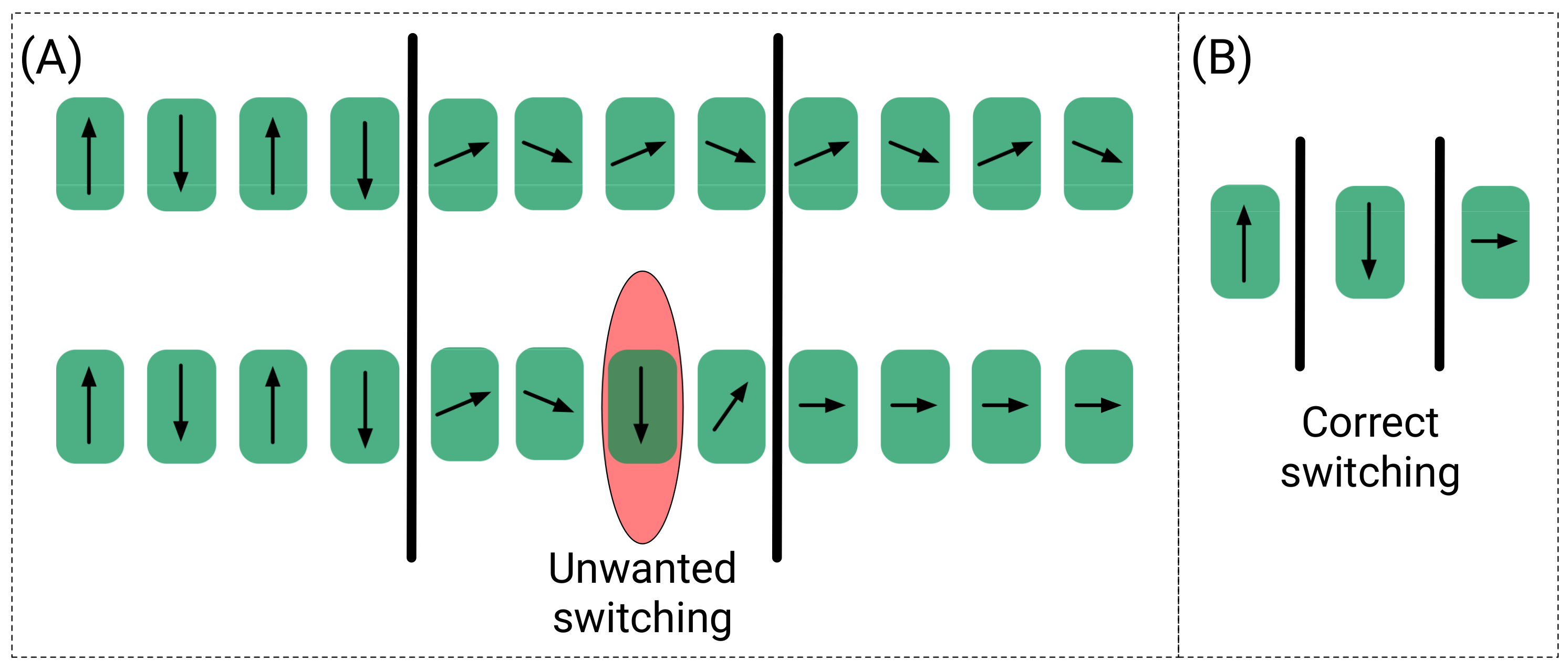
The speed of a synchronous digital circuit is generally related to the clock frequency employed. In NML technology, the clock frequency depends on the number of magnets present inside a clock zone and on the effect of thermal noise. The number of magnets in a clock zone directly affects the duration of the clock pulse. Magnets in a clock zone are forced into the reset state and then, when the clock is removed, they start to switch and reach a stable state that depends on the neighboring elements. The time required for a single magnet to switch from the reset state to a stable state is in the range of 1 ns. So, the larger the number of magnets inside a clock zone, the greater the time required by all of them to switch, because they switch with a cascaded effect. Working at near 0 K temperature, the duration of the clock period can be seen as the sum of the switching time of every magnet. At room temperature, however, the effect of thermal noise must be taken into account. Thermal noise induces small fluctuations in the magnetization. The reset state is unstable, and hence these fluctuations can start an unwanted switching of the magnetization and an error in the information propagation. To avoid this problem, it is important to reduce the number of magnets that are forced in the reset state at the same time, by limiting the number of magnets in a clock zone. A further precaution must be taken. If the clock signal is applied abruptly, the magnetization vector of the magnet will reach the reset state, but it will have heavy fluctuations. These fluctuations may induce unwanted switching of the magnets (see Figure 3A). To avoid them, an adiabatic switching is required. The clock signal is a ramp applied gradually to the clock zone. Magnets switch and reach the reset state with minimum fluctuations, avoiding switching errors. To implement the adiabatic switching, the rising time of the clock signal is generally higher than 10 ns. According to Figure 1C this is the reset time, and it is equivalent to one-third of the clock period.
As a consequence, the clock period is at least equivalent to 30 ns, corresponding to a clock frequency of around 33 MHz. This value of clock frequency is the maximum value that NML circuits can reach if there is more than one magnet inside a clock zone. To increase the speed of NML circuits, the number of magnets inside each clock zone must be reduced to one. In this configuration, there is only one magnet that switches from the reset state to a stable state, so the switching time is lower. Furthermore, with one single element inside a clock zone, it is possible to use an abrupt switch. As discussed in this section, abrupt switches cause fluctuations in the magnetization when it reaches the unstable state. However, with a single element inside a clock zone, the influence of the magnet in the stable state (see Figure 3B) is able to overcome the fluctuations and force the magnets into the correct state. Designing a clock system composed of single magnets for each clock zone is therefore the key to exploiting the true potential of this technology. In Section 3, we describe the clock solution that we propose to reach this goal.
3. Proposed Structure for Independent Control of Piezo-NML Devices
The necessity of independently controlling a nanomagnet requires the ability to physically connect control wires to each individual element. Among the four clock mechanisms mentioned in Section 2, only the STT clock and the magneto-elastic clock enable this option. This option is not available for in-plane NML, because it is not possible to generate a local magnetic field that influences only a single magnet. In the STT case, metal lines must be connected to the top and bottom of the MTJ [15] in order to drive a current through each MTJ. The same structure can be used for the magneto-elastic clock, but the energy consumption in this case is far lower [8], therefore leading to high-speed, low-power NML circuits.
As mentioned in Section 2, the idea behind the magneto-elastic clock is to apply an electric field to a piezoelectric substrate, and then to use the generated mechanical stress to change the magnetization of the nanomagnet. This idea was first proposed in [22], without specifying how to physically apply control signals. We then proposed a variation in [8] based on the same principle, but more technologically feasible. The structure is depicted in Figure 2C. Two electrodes are buried under a piezoelectric substrate, while magnets are placed on top of it. When a voltage is applied to the electrodes, the electric field induces a strain in the substrate and all the magnets between the electrodes are forced into the reset state. Circuits are still divided in clock zones made by many magnets, but there is more freedom in the layout of clock zones. An example can be found in [23].
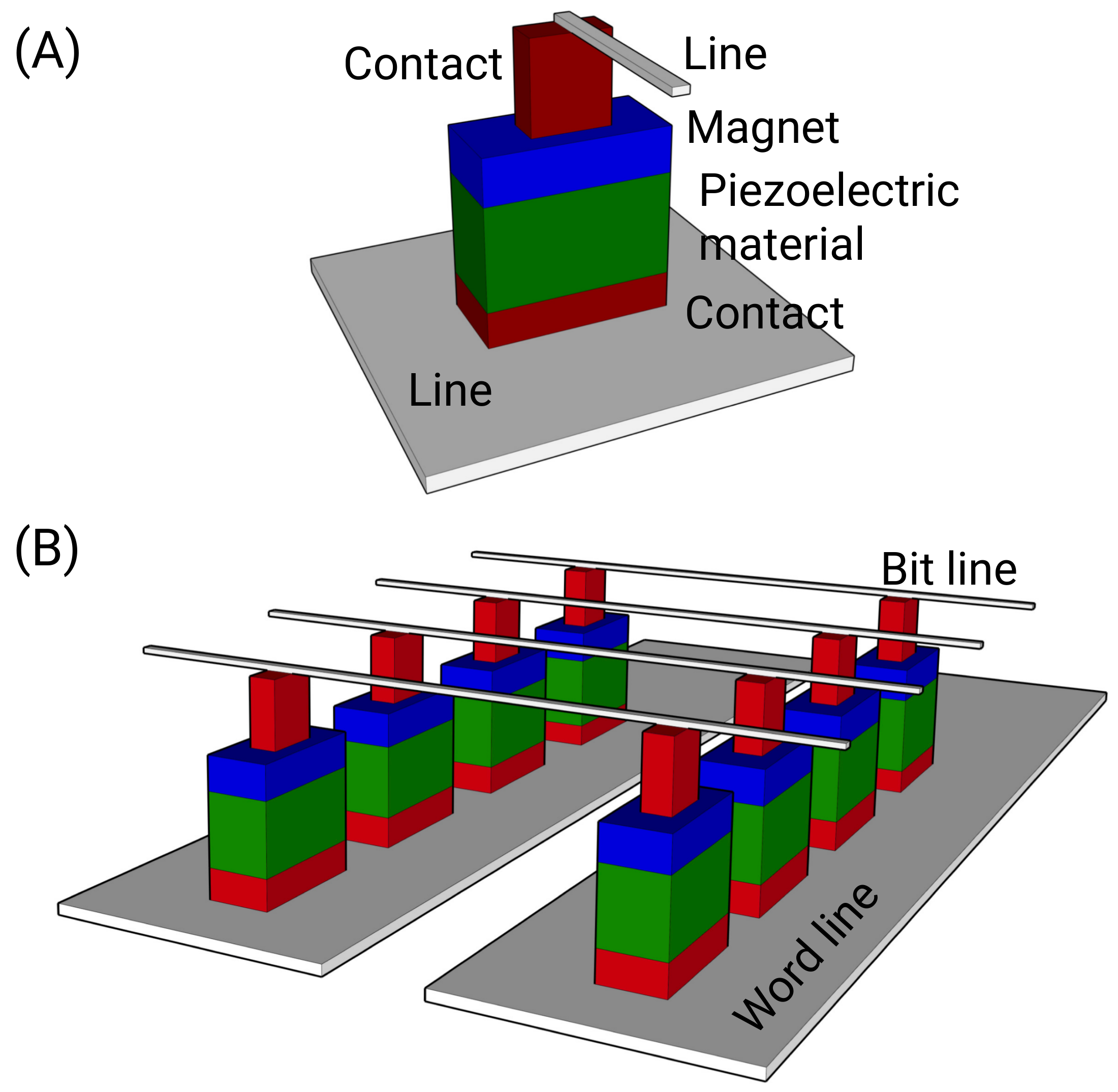
Given that the magneto-elastic clock is the solution that provides the lowest power consumption among all clock mechanisms, we improved our original implementation by designing a clock structure that enables the individual control of nanomagnets. The circuit layout is depicted in Figure 4A, and it is based on the experiments of Chung et al. presented in [7]. Nanomagnets are created on top of a piezoelectric substrate, but the substrate is patterned together with the magnets, so it has the same shape as the magnet. A VIA is used to contact the magnet from the top side, while another electrode is placed at the bottom of the magnet. The bottom electrode is shared among neighbor nanomagnets, simplifying the fabrication process. With this configuration, the electric field is applied out-of-plane and it induces an in-plane strain, orthogonal to the electric field itself. The material used for the nanomagnets is normally Terfenol, an alloy of terbium and iron with very good magnetostriction (i.e., a very good ratio between the applied mechanical stress and the change in the magnetization). There are many options available for the piezoelectric material. The most common is PZT (lead zirconate titanate), but other materials such as barium titanate and polyvinylidenfluoride can also be used [8], providing a lower parasitic capacitance and therefore a lower power consumption.
To control each nanomagnet, and therefore to apply the proper clock signal to each of them, many solutions can be adopted. A possibility is proposed in Figure 4B. Control signals are organized as a grid of wires, resembling the organization of a memory. The “word” lines are connected to the top electrodes, while the “bit” lines are connected to the bottom electrodes. Each wire can be connected to Vdd or to GND. Magnets are placed on the crossing point between the vertical and horizontal wires. Two possible situations can occur: (I) if the horizontal and vertical wires are both connected to Vdd or both to GND, there is no potential difference between the electrodes of the magnet and so the magnet is in switch or in hold phase; (II) if the horizontal and vertical wires are connected one to Vdd and the other to GND, the potential difference leads to the induction of a mechanical stress in the PZT substrate. In this situation, the magnet is forced into the reset state. The organization of circuits in a memory-like structure simplifies the fabrication process, but more complex structures are possible by exploiting additional metal layers to route clock signals, as commonly happens in CMOS devices.
By exploiting this technique, a complete set of logic gates can be implemented. Indeed, majority gates can be used to synthesize elementary gates (e.g., NAND, NOR, etc.) by forcing one of the three inputs to “0” logic or “1” logic [24].
4. Micro-Magnetic Simulations
The physical structure of the basic NML device and circuits was presented in Section 3. To validate the idea, we analyzed a wire made of several chained nanomagnets through the use of finite element simulations. The software MAGPAR was adopted for the investigation of our magneto-elastic devices. The aim of the simulations was to verify the correct behavior of circuits and to analyze at which speed they can operate. Furthermore, we wanted to analyze the impact of the distance among nanomagnets and the effect of different nanomagnet aspect ratios. Both of these quantities are strictly related to the process variations that can arise during the fabrication process. Increasing the distance among neighbor magnets simplifies the fabrication process and reduces the effect of process variation, because a lower-resolution lithography process is required, but it may affect the behavior and performance of circuits. For similar reasons, increasing the aspect ratio of magnets reduces the impact of process variations, but it may affect the switching process. We also investigated how far the value of mechanical stress applied to the magnets can be reduced, in order to determine the minimum power consumption that can be obtained.
4.1. Aspect Ratio Analysis
The energy barrier concept is behind the choice of a magnet’s aspect ratio. Its value is related to the demagnetization energy (which depends on the magnet’s volume, the type of the chosen magnetic material, and the magnet aspect ratio) and the exchange energy. This second component is a quantum term that considers the interaction among neighbor magnets, and since it is a quantum quantity, it only has an impact when magnets are sufficiently close to each other. The exchange energy also depends on the reciprocal magnetization of neighboring cells. When magnets are anti-ferromagnetically coupled (like in the case of horizontal coupling) the exchange energy reduces the energy barrier value. Meanwhile, when they are ferromagnetically coupled (like in the case of vertical coupling), it increases the energy barrier value. The demagnetization energy changes by varying the magnets’ aspect ratio and, consequently, the energy barrier value changes as well. If the aspect ratio is increased, the energy barrier rises, leading to a higher noise immunity when the magnet is in a stable state. The downside of having a high aspect ratio is that it also causes a higher power consumption (if an abrupt switching is performed) or a clock frequency reduction in the case of adiabatic switching.
The circuit speed can be increased in the case of an abrupt switching, but since the switching energy corresponds to the entire energy barrier, the smaller the energy barrier is (and so the aspect ratio) the lower the energy consumption will be. Otherwise, when an adiabatic switching is performed, the value of the energy barrier does not affect the switching energy, but it affects the rise time. This implies that the smaller the energy barrier is, the higher the circuit frequency will be.
So, considering both of the mentioned cases, in order to reduce the energy consumption and increase the circuit speed, it is important to keep the aspect ratio as small as possible. This will unfortunately lead to a reduction of the noise immunity.
In order to demonstrate how the choice of the aspect ratio impacts the required energy, two cases were considered: magnets with dimensions of 50 nm × 60 nm × 10 nm and magnets with dimensions of 60 nm × 90 nm × 10 nm. Both simulations were performed considering magnets made in Terfenol, a distance among magnets equal to 20 nm, and a reset time pulse duration equal to 1 ns. Simulation results obtained with MAGPAR are then reported.
4.1.1. Aspect Ratio: 50 nm × 60 nm × 10 nm
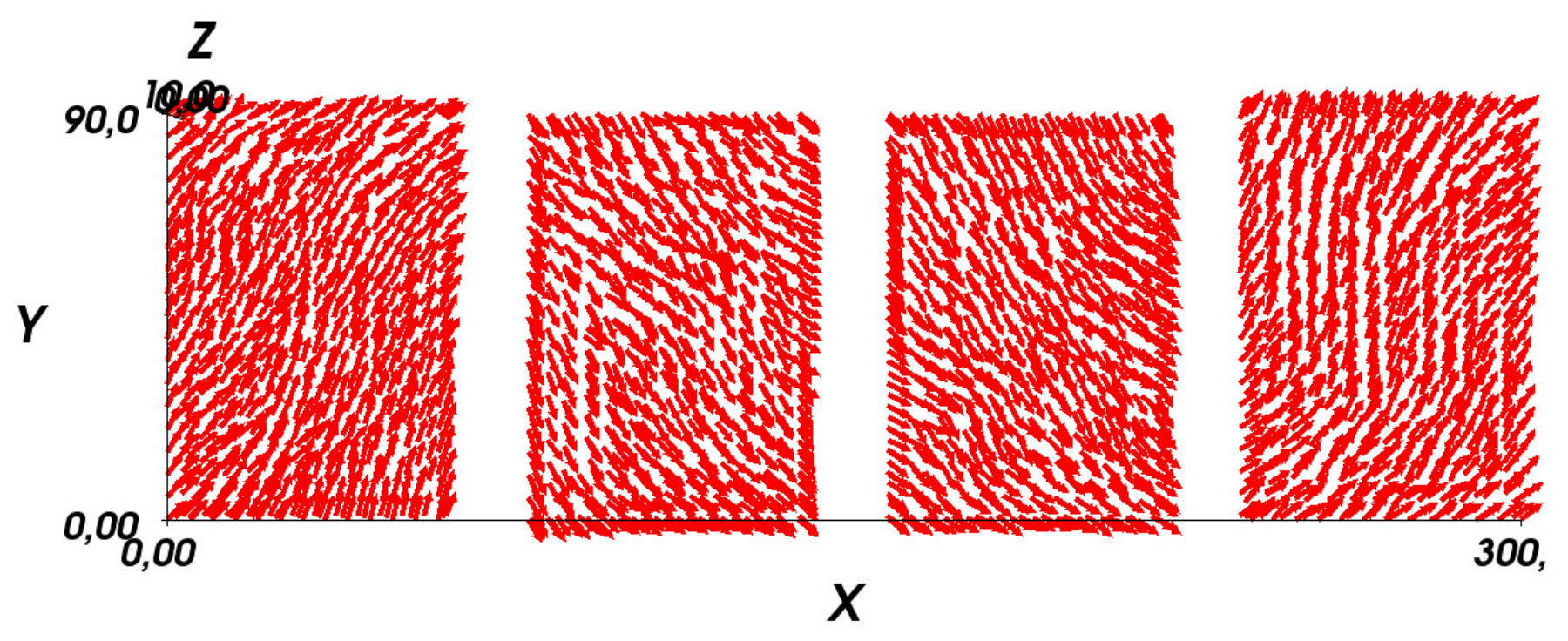
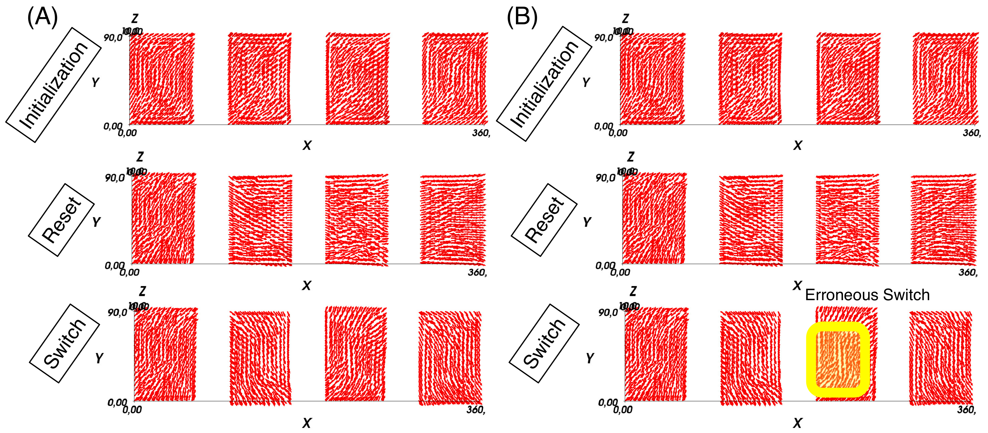
In the very first analysis, we consider a system composed of a chain of four nanomagnets characterized by an aspect ratio of 50 nm × 60 nm × 10 nm [8]. Figure 5 shows the different results obtained on this structure. To better understand the physical behavior of circuits, for each condition, a graph with dynamic evolution of the magnetization for the fourth magnet along the three axes x, y, z is reported.
Within the initialization phase, magnets were set to logic “1” or “0”. Then, as depicted in Figure 5A, a mechanical stress of 30 MPa was applied to devices in order to force them into the reset state. This stress was here modeled as an ideal step with a duration of 1 ns (abrupt switching). Each magnet was controlled independently and, in this first step, they were all forced into the reset state at the same time. Then, the mechanical stress was removed, leaving magnets free to re-align themselves to their final stable state. The mechanical stress was removed from each element one-by-one, starting from the leftmost magnet. This assured a correct signal propagation. The switch state is depicted in Figure 5B.
Moreover, as reported in Figure 5C, the same circuit was analyzed by changing the duration of the mechanical stress pulse. In this second investigation, the pulse was increased from 1 to 6 ns. Here, because of this longer pulse, a more stable behavior was obtained. Indeed, the magnetization graph relative to the last magnet of the chain presented significantly lower fluctuations. We can conclude that with magnets of 50 × 60 × 10 nm, the circuit behaved correctly. The minimum duration for the reset pulse was 1 ns, following the calculation done in Section 2.5, a maximum clock frequency of 333 MHz. A reset pulse of 1 ns was the minimum value of reset time that can be applied to the magnets to have a reliable switching. Figure 6 depicts, for example, what happened when the reset time was reduced to 500 ps.
The magnetization vectors were not perfectly aligned along the x direction. As a consequence, in the switching phase, there was a switching error between the second and third magnets. This led to the conclusion that if the reset time pulse duration was reduced to 500 ps, the circuit did not behave correctly. However, also with a reset pulse duration, the obtained frequency was 10 times higher than normal iNML circuits. These results demonstrate how the independent control of nanomagnets greatly benefits this technology.
4.1.2. Aspect Ratio: 60 nm × 90 nm × 10 nm
While using an aspect ratio of 50 nm by 60 nm leads to a correct behavior and a small switching time, it makes the overall system more vulnerable to the effect of process variations. A variation of a few nanometers in one of the sides of the magnets can significantly change the behavior of the magnets. If the aspect ratio of the magnets is increased to 60 nm × 90 nm × 10 nm, possible variations that arise during the fabrication process have a far smaller impact on the dynamic behavior of magnets. The same analysis made for the previous case was repeated, increasing the size of magnets. Results obtained with this geometry were completely different from the previous ones. Figure 7A depicts the magnetization of the cells obtained by applying a mechanical stress of 30 MPa. Here, the magnetization should rotate toward the x direction according to the reset state. With this specific aspect ratio, the reset state was not reached since the magnetization vectors remained parallel to the y direction. Indeed, since the aspect ratio was increased, magnets presented a higher energy barrier, and the mechanical stress alone was not enough to completely rotate it. In the zoomed picture shown in Figure 7B, the presence of a vortex is noticeable.
Moreover, also by increasing the pulse time from 1 to 6 ns, no stable results could be observed. In order to force magnets into the correct reset state, an extra magnetic field must be applied to the circuit. In Figure 7C, the results obtained by applying a constant extra magnetic field of 10 kA/m are reported. The magnetic field was applied globally to the entire circuit, it was constant, and it had a very low intensity. Such a magnetic field can be generated by permanent magnets, and therefore has no impact on the power consumption.
This result demonstrates that a high aspect ratio required a higher energy to reset the magnets. Moreover, it must also be considered that the reduction of the aspect ratio led to a reduction of the noise immunity of the circuit (increasing the error probability during the information propagation). For this reason, only magnets with dimensions of 60 nm × 90 nm × 10 nm are considered in the following sections.
4.2. Distance Analysis
The distance among neighboring nanomagnets plays a fundamental role in field-coupled technologies. Reducing the distance among elements increases the strength of the interaction, but a higher-resolution lithography fabrication process is required. The aim of this analysis is to understand how far the distance between magnets can be increased to get circuits that still behave correctly. The distance among them was increased respectively to 40, 50, and 60 nm. The following simulations were performed considering: (I) a reset time pulse duration of 1 ns; (II) a constant global magnetic field of 10 kA/m; III) a mechanical stress of 30 MPa (during the reset phase). The magnets’ dimensions were fixed to 60 nm × 90 nm × 10 nm. All magnets were controlled independently, releasing them from the reset state one by one, ensuring maximum clock frequency and maximum reliability.
As depicted in Figure 8A, the circuit behaved correctly with a distance of 40 nm among magnets. Further increasing the distance to 50 nm and 60 nm led to errors during the switching phase. These errors were caused by the reduced influence of the magnetostatic field generated by neighbor magnets. Figure 8B depicts an example of errors that occurred during the switching phase considering a distance of 60 nm. We can therefore conclude that in these conditions, the maximum distance among magnets was 40 nm.
4.3. Physical Structure and Energy Consumption Analysis
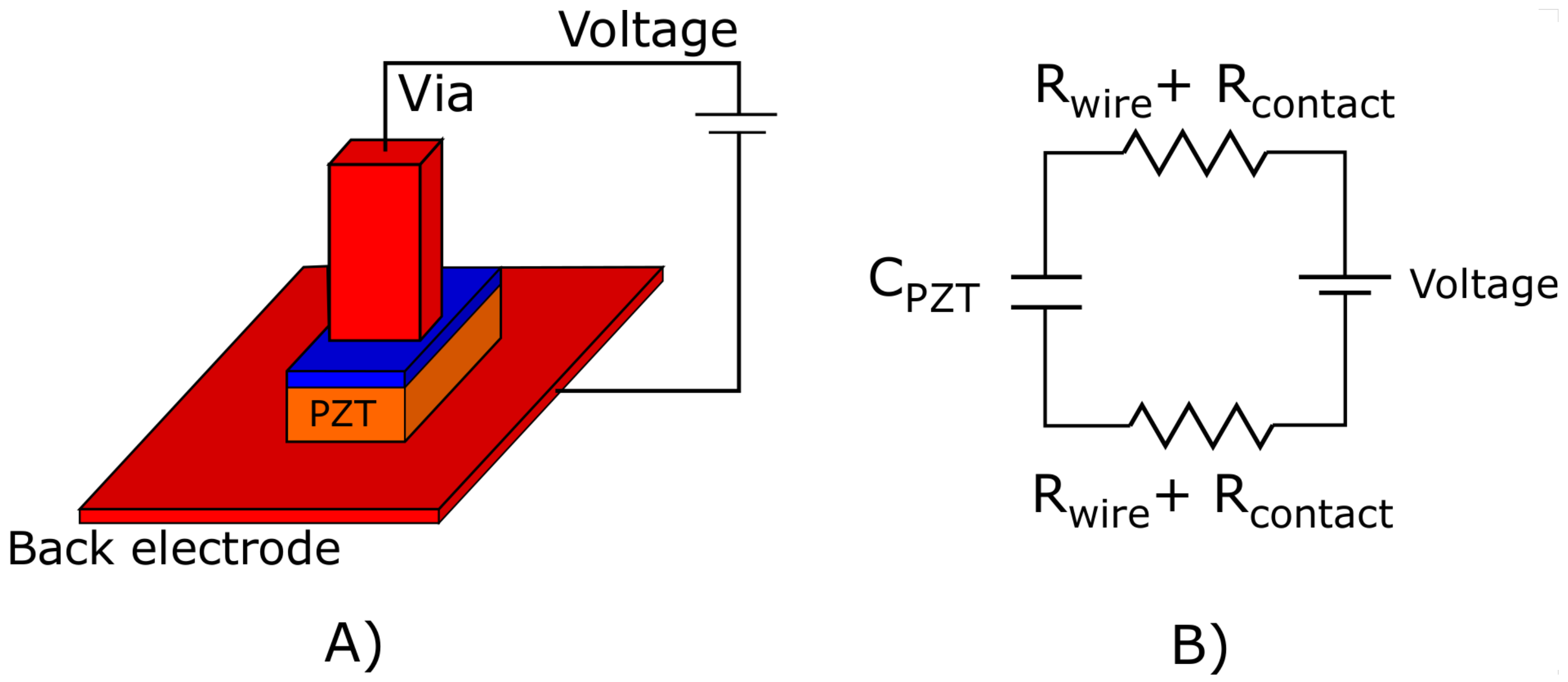
The control of each single nanomagnet requires a sophisticated fabrication process. Indeed, the whole structure can be seen as a capacitor, where the electrodes are the plates and the piezoelectric layer is the insulator. The physical structure is depicted in Figure 9A, while the equivalent electric circuit is presented in Figure 9B. The energy consumption in this type of NML circuit is related to the charge and discharge of the parasitic capacitance.
In the worst-case scenario, the energy consumption does not depend on the value of resistances, but only on the value of the parasitic capacitance of the piezoelectric layer. It is given by Equation (1):
where is the capacitance of the piezoelectric layer (PZT in this case) and V is the applied voltage. The capacitance can be evaluated as in Equation (2):
where is the relative dielectric constant of the PZT, is the thickness of PZT, and and are respectively the height and width of the considered nanomagnets. V is the applied voltage and is the capacitance of the parasitic capacitor. The applied voltage can be estimated as in Equation (3):
where Y is the Young modulus of the considered magnetic material (i.e., Terfenol), is the magnet’s width, is the applied mechanical stress, and is the piezoelectric coefficient of the PZT material. describes the correlation of an electric field applied perpendicularly to the structure and a mechanical stress generated orthogonally to it, therefore in the magnets’ plane. The values of the parameters were taken from [8] and are summarized in Table 1.
The value of can vary substantially, depending on the particular fabrication process used to create the PZT layer. Considering the minimum and maximum values of , the voltage that must be applied to the magnet varied from 0.3 to 0.7 Volts. Furthermore, the value of can also change depending on the PZT fabrication process. Considering the minimum and maximum values of the dielectric constant, the parasitic capacitance varied from 0.159 fF to 0.690 fF. As a result, the energy consumption for each magnet can vary from a minimum value of 15 aJ to a maximum value of 360 aJ. The energy consumption depends heavily on the value of voltage required to reset the magnets, which is proportional to the value of mechanical stress used. The energy consumption obtained was very low, but to further reduce it, circuits were simulated using a smaller value of mechanical stress. At first, MAGPAR simulation was performed by halving the mechanical stress to 15 MPa. It can be seen from Figure 10A that the magnetization vectors of the magnets were oriented along the x-axis. So, a mechanical stress of 15 MPa was still sufficient to successfully reset the magnets.
A further reduction to 10 MPa highlighted that this value was insufficient to guarantee the correct reset of the magnets. Looking at Figure 10B, it can be noticed that the magnetization vectors were not perfectly aligned in the x direction and the y component was not equal to zero. For this reason, only mechanical stress values equal to or greater than 15 MPa could be used to obtain a correct reset of the magnets (and thus a correct circuit behavior). The magnetization components along the x-, y-, and z-axes can be better observed in Figure 10C. The magnetization vectors should be oriented along the x direction, with the y component equal to zero. However, the magnetization along the y direction was not zero, but it tended respectively to −1, +1, and −1 again. Reducing by 2 times the applied voltage reduced the energy consumption by 4 times. The resulting energy consumption was therefore in the range of 4–90 aJ for each magnet—one of the smallest values among all NML types [8].
5. Conclusions
NML technology has a lot of potential. To exploit this potential, a proper clock solution must be adopted. In this work, we presented a clock solution based on the magneto-elastic effect that is not only compatible with current fabrication processes, but that makes it possible to notably increase operating frequency (up to 10 times) while keeping the energy consumption at an extremely low level. We presented the physical structure of the circuits, considering both the magnets and the clock wires required to control them. Then, as a novelty in the literature, we validated the proposed solution and its performance using physical simulations. The system that we propose not only enables high-speed NML circuits with very low energy consumption to be obtained, but it also provides a high tolerance to process variations.
Author Contributions
Conceptualization and Writing—Review & Editing, G.T.; Investigation and Validation, L.D.; Conceptualization and Supervision, M.V.
Funding
This research received no external funding.
Conflicts of Interest
The authors declare no conflict of interest.
References
- Stamps, R.L.; Breitkreutz, S.; Åkerman, J.; Chumak, A.V.; Otani, Y.; Bauer, G.E.; Thiele, J.-U.; Bowen, M.; Majetich, S.A.; Kläui, M.; et al. The 2014 magnetism roadmap. J. Phys. D Appl. Phys. 2014, 47, 333001. [Google Scholar] [CrossRef] [Green Version]
- International Technology Roadmap of Semiconductors 2.0. Beyond CMOS, 2015. Available online: http://public.itrs.net (accessed on 3 September 2018).
- Csaba, G.; Porod, W. Behavior of Nanomagnet Logic in the Presence of Thermal Noise. In Proceedings of the International Workshop on Computational Electronics, Pisa, Italy, 26–29 October 2010; pp. 1–4. [Google Scholar]
- Turvani, G.; Riente, F.; Cairo, F.; Vacca, M.; Garlando, U.; Zamboni, M.; Graziano, M. Efficient and reliable fault analysis methodology for nanomagnetic circuits. Int. J. Circuit Theory Appl. 2016. [Google Scholar] [CrossRef]
- Alam, M.T.; DeAngelis, J.; Putney, M.; Hu, X.S.; Porod, W.; Niemier, M.; Bernstein, G.H. Clocking scheme for nanomagnet QCA. In Proceedings of theInternational Conference on Nanotechnology, Hong Kong, China, 2–5 August 2007; pp. 403–408. [Google Scholar]
- Alam, M.T.; Siddiq, M.J.; Bernstein, G.H.; Niemier, M.; Porod, W.; Hu, X.S. On-chip Clocking for Nanomagnet Logic Devices. IEEE Trans. Nanotechnol. 2009, 9, 348–351. [Google Scholar] [CrossRef]
- Chung, T.K.; Keller, S.; Carman, G.P. Electric-field-induced reversible magnetic single-domain evolution in a magnetoelectric thin film. Appl. Phys. Lett. 2009, 94, 132501. [Google Scholar] [CrossRef]
- Vacca, M.; Graziano, M.; Crescenzo, L.D.; Chiolerio, A.; Lamberti, A.; Balma, D.; Canavese, G.; Celegato, F.; Enrico, E.; Tiberto, P.; et al. Magnetoelastic clock system for nanomagnet logic. IEEE Trans. Nanotechnol. 2014, 13, 963–973. [Google Scholar] [CrossRef]
- Scholz, W.; Fidler, J.; Schrefl, T.; Suess, D.; Forster, H.; Tsiantos, V. Scalable Parallel Micromagnetic Solvers for Magnetic Nanostructures. Comput. Mater. Sci. 2003, 28, 366–383. [Google Scholar] [CrossRef]
- Niemier, M.T.; Bernstein, G.H.; Csaba, G.; Dingler, A.; Hu, X.S.; Kurtz, S.; Liu, S.; Nahas, J.; Porod, W.; Siddiq, M.; et al. Nanomagnet logic: Progress toward system-level integration. J. Phys. Condens. Matter 2011, 23, 34. [Google Scholar] [CrossRef] [PubMed]
- Nikonov, D.E.; Young, I.A. Benchmarking of beyond-cmos exploratory devices for logic integrated circuits. IEEE J. Explor. Solid-State Comput. Devices Circuits 2015, 1, 3–11. [Google Scholar] [CrossRef]
- Zhang, S.; Xia, R.; Lebrun, L.; Anderson, D.; Shrout, T.R. Piezoelectric materials for high power, high temperature applications. Mater. Lett. 2005, 59, 3471–3475. [Google Scholar] [CrossRef]
- Das, J.; Alam, S.M.; Bhanja, S. Nano Magnetic STT-Logic Partitioning For Optimum Performance. IEEE Trans. VLSI Comput. 2014, 22, 90–98. [Google Scholar] [CrossRef]
- Li, J.; Ndai, P.; Goel, A.; Salahuddin, S.; Roy, K. An alternate design paradigm for robust spin-torque transfer magnetic ram (stt mram) from circuit/architecture perspective. In Proceedings of the 2009 Asia and South Pacific Design Automation Conference, Yokohama, Japan, 19–22 January 2009; pp. 841–846. [Google Scholar]
- Turvani, G.; Bollo, M.; Vacca, M.; Cairo, F.; Zamboni, M.; Graziano, M. Design of mram based magnetic logic circuits. IEEE Trans. Nanotechnol. 2017, 16, 851–859. [Google Scholar] [CrossRef]
- Bollo, M.; Turvani, G.; Zamboni, M.; Das, J.; Bhanja, S.; Graziano, M. Design of nml circuits based on m-ram. In Proceedings of the 2015 IEEE 15th International Conference on Nanotechnology (IEEE-NANO), Rome, Italy, 27–30 July 2015; pp. 1339–1342. [Google Scholar]
- Turvani, G.; Riente, F.; Plozner, E.; Schmitt-Landsiedel, D.; Breitkreutz-v. Gamm, S. A compact physical model for the simulation of pnml-based architectures. AIP Adv. 2017, 7, 056005. [Google Scholar] [CrossRef]
- Riente, F.; Ziemys, G.; Mattersdorfer, C.; Boche, S.; Turvani, G.; Raberg, W.; Luber, S.; Breitkreutz-v. Gamm, S. Controlled data storage for non-volatile memory cells embedded in nano magnetic logic. AIP Adv. 2017, 7, 055910. [Google Scholar] [CrossRef]
- Breitkreutz, S.; Eichwald, I.; Ziemys, G.; Schmitt-Landsiedel, D.; Becherer, M. Influence of the domain wall nucleation time on the reliability of perpendicular nanomagnetic logic. In Proceedings of the 14th IEEE International Conference on Nanotechnology, Toronto, ON, Canada, 18–21 August 2014; pp. 104–107. [Google Scholar]
- Cairo, F.; Turvani, G.; Riente, F.; Vacca, M.; Breitkreutz-v. Gamm, S.; Becherer, M.; Graziano, M.; Zamboni, M. Out-of-plane nml modeling and architectural exploration. In In Proceedings of the 2015 IEEE 15th International Conference on Nanotechnology (IEEE-NANO), Rome, Italy, 27–30 July 2015; pp. 1037–1040. [Google Scholar]
- Chiolerio, A.; Quaglio, M.; Lamberti, A.; Celegato, F.; Balma, D.; Allia, P. Magnetoelastic coupling in multilayered ferroelectric/ferromagnetic thin films: A quantitative evaluation. Appl. Surf. Sci. 2012, 258, 8072–8077. [Google Scholar] [CrossRef]
- Atulasimha, J.; Bandyopadhyay, S. Hybrid spintronic/straintronics: A super energy efficient computing scheme based on interacting multiferroic nanomagnets. In Proceedings of the 2012 12th IEEE International Conference on Nanotechnology, Birmingham, UK, 20–23 August 2012. [Google Scholar]
- Giri, D.; Vacca, M.; Causapruno, G.; Zamboni, M.; Graziano, M. Modeling, design, and analysis of magnetoelastic nml circuits. IEEE Trans. Nanotechnol. 2016, 15, 977–985. [Google Scholar] [CrossRef]
- Sarvaghad-Moghaddam, M.; Orouji, A.A.; Houshmand, M. A Multi-Objective Synthesis Methodology in Quantum-Dot Cellular Automata Technology. CoRR. 2016. Available online: http://arxiv.org/abs/1606.00203 (accessed on 3 September 2018).
Figure 1.
Nanomagnetic logic (NML) principles: (A) NML cells can encode binary information according to their magnetization. (B) Wire of nanomagnets. (C) NML clocking signals. (D) Effect of a multi-clicking system on NML devices. (E) Example of NML circuit, a half adder. The clock zones are highlighted using different colors.

Figure 2.
NML implementation: (A) Magneto tunnel junction (MTJ). (B) Perpendicular NML (pNML). (C) Piezo-NML. STT: spin-transfer torque.
Figure 2.
NML implementation: (A) Magneto tunnel junction (MTJ). (B) Perpendicular NML (pNML). (C) Piezo-NML. STT: spin-transfer torque.

Figure 3.
Switching in an NML circuit. (A) Switching error due to the presence of fluctuations in the reset state and many magnets in a clock zone. (B) Correct switching due to the presence of a single magnet for each clock zone.
Figure 3.
Switching in an NML circuit. (A) Switching error due to the presence of fluctuations in the reset state and many magnets in a clock zone. (B) Correct switching due to the presence of a single magnet for each clock zone.

Figure 4.
(A) Single piezo-NML device. (B) Matrix of piezo-NML devices.

Figure 5.
MAGPAR simulations of nanomagnets with dimensions: 50 nm × 60 nm × 10 nm: (A) Reset stage obtained by applying a mechanical stress of 30 MPa. High fluctuations are visible. (B) Switch stage: the field is removed and magnets are free to realign themselves according to the input. (C) Reset stage. In order to avoid fluctuations, the pulse duration was increased from 1 to 6 ns.

Figure 6.
MAGPAR simulation: the pulse duration was decreased from 1 ns to 500 ps. In this condition, the magnetization vector was not perfectly aligned to the y-axis.
Figure 6.
MAGPAR simulation: the pulse duration was decreased from 1 ns to 500 ps. In this condition, the magnetization vector was not perfectly aligned to the y-axis.

Figure 7.
MAGPAR simulations of nanomagnets with dimensions: 60 nm × 90 nm × 10 nm. (A) Initialization phase (all magnets’ magnetizations were parallel to the y-axis. (B) With this aspect ratio a higher energy was required to reset magnets. Here, the mechanical stress was not sufficient to force devices into the Reset state. Indeed, if no external field was applied, a vortex could be generated. (C) Simulation results obtained by applying an additional global and constant magnetic field.

Figure 8.
MAGPAR simulations. (A) The distance among nanomagnets was set to 40 nm. (B) The distance among nanomagnets was set to 60 nm. With this higher spacing, some switching errors may occur.
Figure 8.
MAGPAR simulations. (A) The distance among nanomagnets was set to 40 nm. (B) The distance among nanomagnets was set to 60 nm. With this higher spacing, some switching errors may occur.

Figure 9.
(A) Physical circuit structure. (B) Equivalent electric model.

Figure 10.
MAGPAR simulations. (A) By applying a mechanical stress of 15 MPa it was still possible to force magnets into the Reset state. (B) If the mechanical stress was further decreased, it was not possible to align the magnetization parallel to the x-axis.
Figure 10.
MAGPAR simulations. (A) By applying a mechanical stress of 15 MPa it was still possible to force magnets into the Reset state. (B) If the mechanical stress was further decreased, it was not possible to align the magnetization parallel to the x-axis.


Table 1.
Parameters for energy calculation.
| 60 nm | |
| 90 nm | |
| Y (Terfenol) | 80 GPa |
| (PZT) | 30–80 |
| 40 nm | |
| 300–1300 | |
| 30 MPa |
© 2018 by the authors. Licensee MDPI, Basel, Switzerland. This article is an open access article distributed under the terms and conditions of the Creative Commons Attribution (CC BY) license (http://creativecommons.org/licenses/by/4.0/).
Share and Cite
MDPI and ACS Style
Turvani, G.; D’Alessandro, L.; Vacca, M. Physical Simulations of High Speed and Low Power NanoMagnet Logic Circuits. J. Low Power Electron. Appl. 2018, 8, 37. https://0-doi-org.brum.beds.ac.uk/10.3390/jlpea8040037
AMA Style
Turvani G, D’Alessandro L, Vacca M. Physical Simulations of High Speed and Low Power NanoMagnet Logic Circuits. Journal of Low Power Electronics and Applications. 2018; 8(4):37. https://0-doi-org.brum.beds.ac.uk/10.3390/jlpea8040037
Chicago/Turabian StyleTurvani, Giovanna, Laura D’Alessandro, and Marco Vacca. 2018. "Physical Simulations of High Speed and Low Power NanoMagnet Logic Circuits" Journal of Low Power Electronics and Applications 8, no. 4: 37. https://0-doi-org.brum.beds.ac.uk/10.3390/jlpea8040037
Note that from the first issue of 2016, this journal uses article numbers instead of page numbers. See further details here.