1. Introduction
The Federal Communications Commission (FCC), in 2002, offered a 3.1–10.6 GHz ultra-wideband frequency (UWB) range, for the implementation of very high data rate wireless communication links [
1]. The FCC set an upper limit on highest power spectral density to −41.3 dBm/MHz over the 3.1–10.6 GHz frequency range, so that the newly designed wireless communication devices could not interfere with the wireless services existing in the same local area network [
1,
2,
3]. This upper limit for power spectral density makes the UWB technology suitable for many interesting wireless applications, such as wireless personal area networks (WPAN), medical imaging, short-range radars for vehicles and wireless sensor nodes [
4,
5]. It gives reasons for low-power very-large scale integration (VLSI) design industries and researchers to develop low-power, low-noise, and reliable UWB radio-frequency integrated circuits (RFICs) for these applications. Moreover, continuous shrinking in complementary metal oxide semiconductor (CMOS) chip fabrication technologies and split manufacturing techniques in RF designs [
6,
7], makes it possible to design and fabricate RFICs on the nanometer scale [
8,
9].
LNA as a primary module of UWB wireless communication receiver requires designers to meet many challenges like 50 Ω input matching, a low noise figure, flat gain, low power, and the receiver’s stability across the complete UWB frequency range [
2,
3,
9]. Two frequently used UWB LNA topologies by many researchers are common-source (CS) [
8,
10,
11,
12,
13,
14,
15,
16] and common-gate (CG) [
2,
3,
4,
5,
17] (
Figure 1). The CS-topology is suitable to design LNAs for narrow and wide-band matching with high power gain (
S21). However, using the proper band-pass network, CS topologies can also be used for wideband LNA designs, but it degrades the gain and noise performance of the LNA. A common-source LNA with impedance feedback topology (
Figure 1c) is also famous among some researchers [
10,
11,
12,
13,
17]. However, the noise figure of a resistive feedback LNA is higher than that of CS topology. Distributed amplifiers (DA) (
Figure 1d) are favored by some researchers to realize flat gain LNA for UWB [
18,
19]. The average power gain of DA is around 8–10 dB [
18,
19]. Active inductor-based input matching techniques (
Figure 1e) can also be used for gain flatness in CG-topology [
20]. However, due to the inclusion of an additional metal-oxide semiconductor (MOS) device used as an active inductor at the input, it increases
NF as compared to traditional CG-LNA. For example,
NF of the LNA proposed in [
20] is greater than 4.5 dB.
This paper reports a design of a low-power LNA using CG feedback-body biased topology for an UWB frequency. A CG configuration provides a very simple technique for UWB input impedance matching by setting 1/
gm equal to 50 Ω, where gm is the transconductance of CG transistor. Implementation of feedback-body biasing for input CG transistor leads to the further decrease in the power supply (
Vdd) due to the decrease in threshold voltage, which results from a decrease in power consumption. The advantage of a wideband input matching capability and utilizing the body-biasing to decrease power consumption brought our attention to the traditional CG LNA topologies for the 3.1–10.6 GHz UWB frequency. This paper is organized as follows:
Section 2 describes the proposed LNA design methodology for the proposed LNA. In
Section 3, the results of the proposed LNA circuit and comparison with the previous work are presented. Finally,
Section 4 concludes this paper.
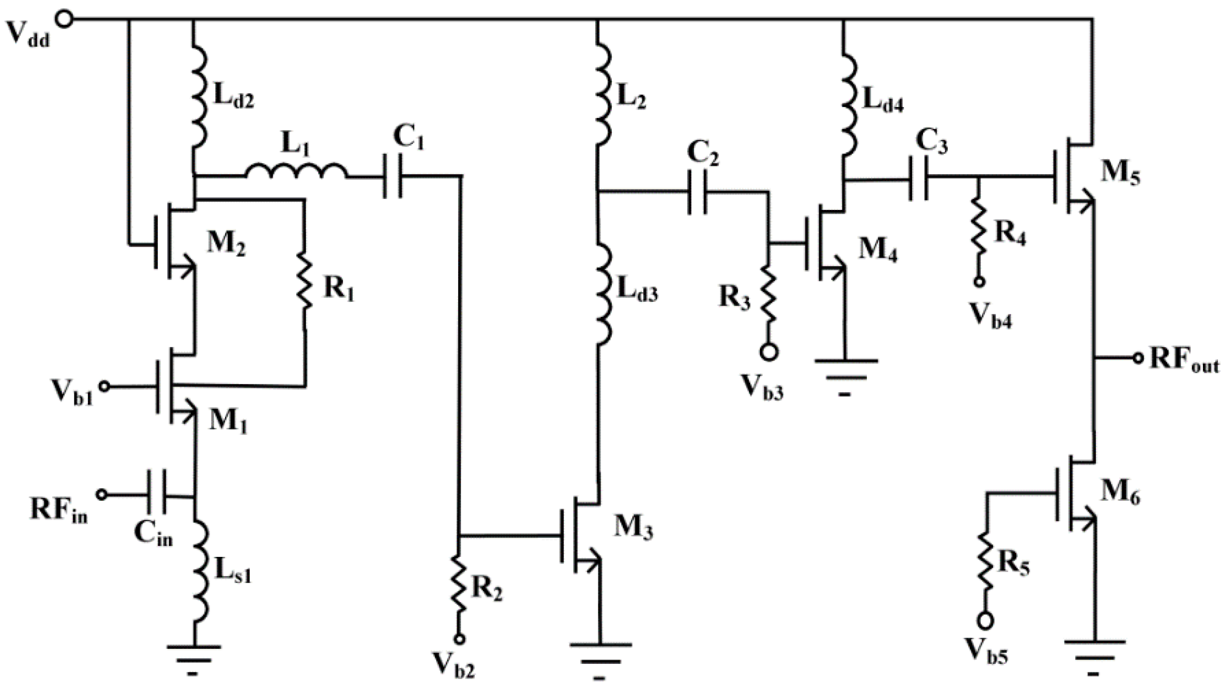
2. Operational Principle and Circuit Implementation
The circuit diagram of the proposed UWB LNA shown in
Figure 2 consists of four stages. At the input side, a common-gate cascode topology has been used to achieve wideband input matching. The source inductor (
Ls1) and gate-source parasitic capacitance (
Cgs1) dictates the input resonance frequency of the CG-stage. The transistor M
1 has been configured to feedback-body biasing through the feedback resistor
R1 connected to drain terminal of M
2, to boost-up the noise figure performance and the power consumption, whereas the transistor M
2 is cascoded with M
1 to enhance the gain of the first stage. The CG first stage has been cascoded with two stages of common source configuration using transistors M
3 and M
4 respectively, to enhance the gain and bandwidth proposed for UWB LNA. In first CS stage,
Ld3 serves as a series peaking inductor, which increases the gain flatness. At the output side, a buffer stage has been used for enhancing the output matching (
S22) performance of the proposed LNA. The output of the transistor is tuned by a parallel LC resonating circuit, in which an inductor (
Ld4) resonates with the total gate-drain parasitic capacitances (i.e.,
Cgd4 +
Cgd5) of the transistors M
4 and M
5, respectively. The output is taken from the source terminal of transistor M
5 whereas M
6 behaves as a saturated load.
The capacitors
Cin,
C1,
C2 and
C3 are the coupling capacitors, whereas the resistors
R2 to
R5 are used as biasing resistors. Maximum power flow from receiver end to the load end is one of the important requirements for an LNA design, and for this purpose, a parallel to series LC network has been used between common gate first stage’s output and the input of second stage. In this, drain inductor (
Ld2) and gate-drain parasitic capacitance (
Cgd2) of M
2 are figured as parallel resonance circuit resonating at
, whereas inductor
L1 and the capacitance
C1 are used to form series resonance circuit resonating at
. A frequency response equivalent to a band-pass filter can be achieved when parallel LC tank resonates at the same centerfrequency at which series LC tank does. This condition can be achieved when
, i.e.,
.
Table 1 provides the parameter values for the proposed LNA design.
2.1. Forward Body Baising to Decrease Power Consumption
Due to the cascode architecture of transistors M
1 and M
2, it demands high
Vdd supply. This limits the design of LNA to low power consumption. To mitigate this problem, the forward-body bias technique has been implemented in this paper, to operate the proposed UWB LNA at lower
Vdd supply of 0.7 V. The transistor M
1 is the key-element in deciding the input impedance matching and noise figure of the complete LNA circuit, and to isolate it from transistor M
2, the forward-body bias technique has been applied only to M
1. This provides more degrees of freedom in finalizing the device dimensions of M
2, to keep transconductance (
gm2) constant and to provide constant current to primary amplifying transistor M
1 [
19,
20,
21]. The threshold voltage
Vth of the transistor M
1 can be characterized by:
where
Vt0 is the threshold voltage for zero body-to-source voltage (i.e.,
VBS =0),
γ0 is a constant that describes body-effect and usually has a value in the range of 0.3–0.4 V and
φf is the bulk Fermi-potential. It is clear from Equation (1) that applying a forward voltage to body terminal will reduce the threshold voltage of MOS device which in turn helps in reducing the power consumption.
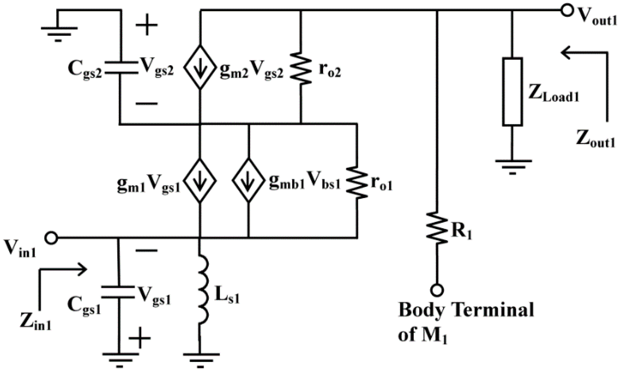
2.2. Frequency Response of S11 and S22
In this section, the proposed LNA design has been analyzed for the frequency response of the input reflection coefficient (
S11) and the output reflection coefficient (
S22). The approximate expressions for
S11 and
S22 have been derived here using the small-signal model of the proposed LNA shown in
Figure 3, where the effect of the input capacitor (
Cin) on the overall input impedance (
Zin) has been neglected.
After using fundamental network theorems, the input impedance of the proposed LNA design can be obtained as:
where Z
s1(
ω) is impedance of parallel LC tank and
ZX(
ω) can be expressed as:
where
gm1,
gm2 are transconductances and 1/
ro1, 1/
ro2 are drain-to-source channel conductance of M
1 and M
2 respectively. Back-gate transconductance of M
1 is denoted by
gmb1 and
ZLoad1 is the total load impedance connected at the drain of transistor M
2. In Equation (3), assuming
ro1 >> 1 and
ro2 >> 1, then at the input parallel resonance condition set up by
Ls1 and
Cgs1 and the input impedance
Zin(ω) can be approximated as:
The input reflection coefficient (
S11) can be expressed as:
In general,
S11 ≤ −10 dB is an essential requirement for the entire frequency of interest. From Equations (4) and (5) we have:
For the output reflection coefficient (
S22), output impedance estimated by looking into the output buffer transistor M
5 is keeping input of the buffer stage as zero. The output impedance of the proposed LNA can be expressed as:
where
Z4(ω) is the impedance of the LC tank formed by
Ld4 with (
Cgd4 +
Cgd5).
Cgd4 is the gate-to-drain parasitic capacitance of transistor M
4, whereas
Cgs5 and
gm5 are the gate-source parasitic capacitance and transconductance of the transistor M
5, respectively. The output reflection coefficient (
S22) is given by:
2.3. Noise Figure Analysis
The noise equivalent model of the proposed UWB is shown in
Figure 4. The input CG transistor M
1 plays a significant role in overall the noise figure of the LNA while the noise contribution of cascoded transistor M
2 and other successive stages is very small. In
Figure 4, the main noise sources included are: the thermal noise due to signal source resistance
Rs represented by
, the gate-induced noise of M
1 represented by
and the channel-induced thermal noise of M
1 represented by
where,
k is the Boltzmann constant,
T is the temperature in Kelvin,
is noise bandwidth,
δ is the coefficient of gate-induced noise and
γ is the coefficient of channel-induced thermal noise. The
gg and
gd0 are given by
and
respectively, where
gg is the equivalent gate conductance and
gd0 is the zero-bias drain conduction of transistor M
1. Another important noise source of MOS transistor of noise due to the bulk-resistance (
RB) given by
[
22]. This bulk-resistance is distributive in nature, which is very difficult of analyze quantitatively [
23]. Furthermore, this noise is also not correlated with the gate induced noise and the channel induced thermal noise. However, the effect of noise due to bulk resistance can be decreased by decreasing the value of
gmb1 and is clear from the expression of
gmb1 given by:
This will be possible if we apply a forward voltage to the body terminal of M
1. The correlation coefficient
c between induced gate noise (
) and channel induced thermal noise (
) is also ignored here for simplifying our noise figure analysis. The noise figure of the proposed LNA can be expressed as:
where
,
and
are the rms output noise voltages at the drain terminal of M
2 due to
,
and
, respectively. The
,
and
can be expressed as:
and:
Respectively. Substituting the Equations (11)–(13) in Equation (10), we get the noise figure expression of the proposed UWB LNA as:
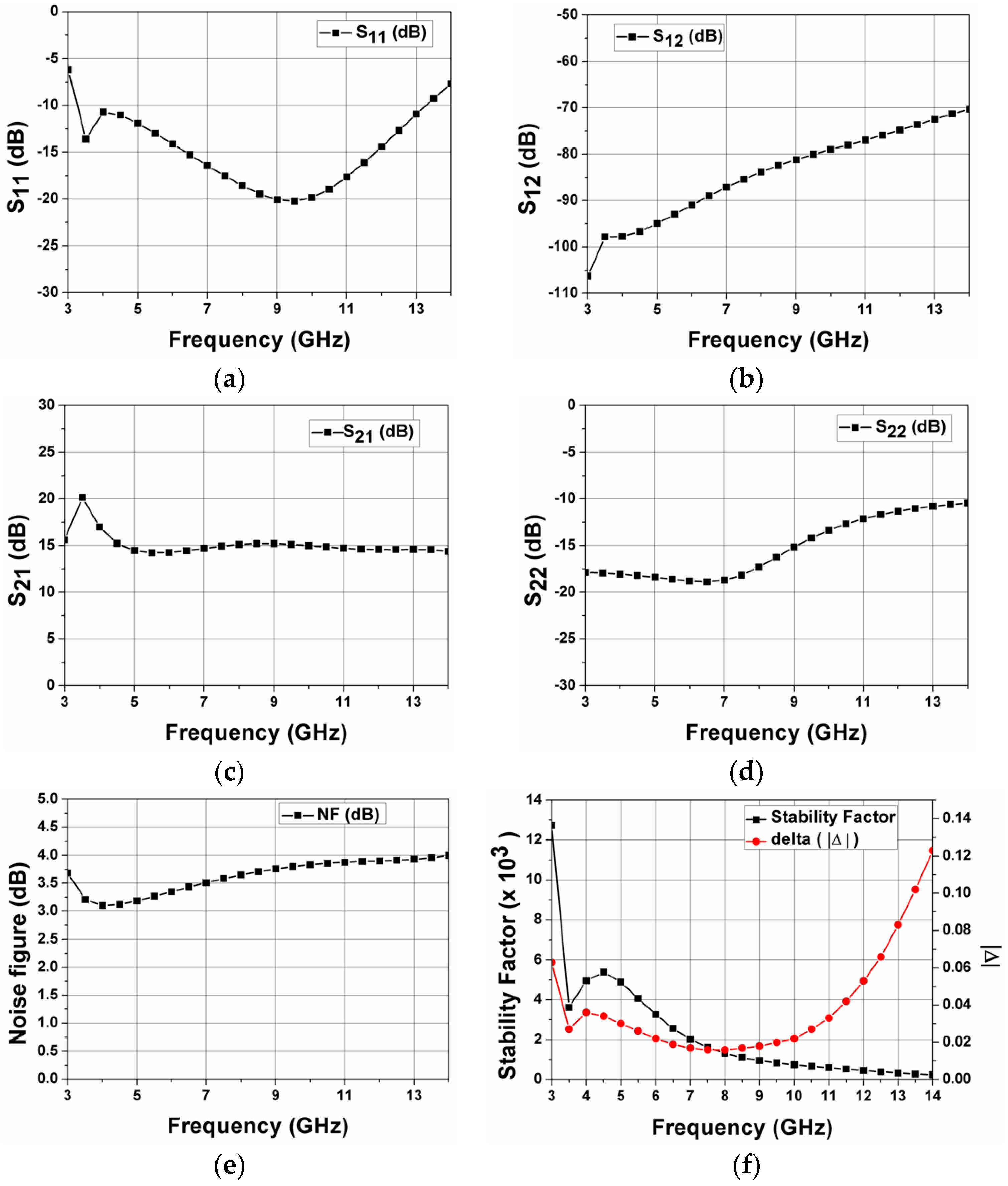
3. Simulation Results
The proposed LNA is designed and simulated using a 90 nm CMOS process for 3–14 GHz UWB frequency range. The simulation results for
S-parameters, noise figure and stability of the proposed FBB UWB LNA are shown in
Figure 5. It can be observed from
Figure 5a that the proposed LNA UWB input matching with
S11has less than −10.6 dB for a frequency range of 3.3 GHz to 13.0 GHz. For this purpose, the transconductance (
gm1) of M
1 was set to 26 mS so that 1/
gm1 ≈ 38.4 Ω, so that the difference from the 50 Ω antenna impedance will be contributed to by the successive stages in the LNA architecture. Due to the CG cascode topology the proposed UWB LNA has a very high reverse isolation (
S12) of less than −72.4 dB was achieved throughout the complete UWB range (
Figure 5b).
The frequency response for power gain (
S21) is shown in
Figure 5c and it can be observed from the figure that
S21 was greater than 14.2 dB throughout the frequency range of 3.0 GHz to 13.0 GHz. The proposed LNA shows a flat
S21 for 15.7 ± 0.5 dB for a frequency range of 4.5 GHz to 13.0 GHz whereas, the output reflection coefficient (
S22) was less than −10.8 dB for the 3.0 GHz to 13.0 GHz frequency range (
Figure 5d). The noise figure plot of the LNA proposed is shown in
Figure 5e and it can be observed from the noise figure versus frequency plot, NF was ranging from 3.0 dB to 4.0 dB for the complete UWB frequency range.
In extension to the parameters discussed earlier for the designing of LNA, another significant parameter to be considered is the Stability factor (
K). The absolute stability is an essential requirement for the designed LNA. The stability factor can be expressed as:
The stability factor (
K) should be greater than 1 and the delta (|Δ|) should be less than 1 for an unconditional stability of a system throughout the complete UWB frequency range.
Figure 5f shows the stability of the proposed LNA design, where minimum value obtained for
K was equal to 330 at 13.0 GHz, which is far greater than unity and the value of delta (|Δ|) at less than 0.12.
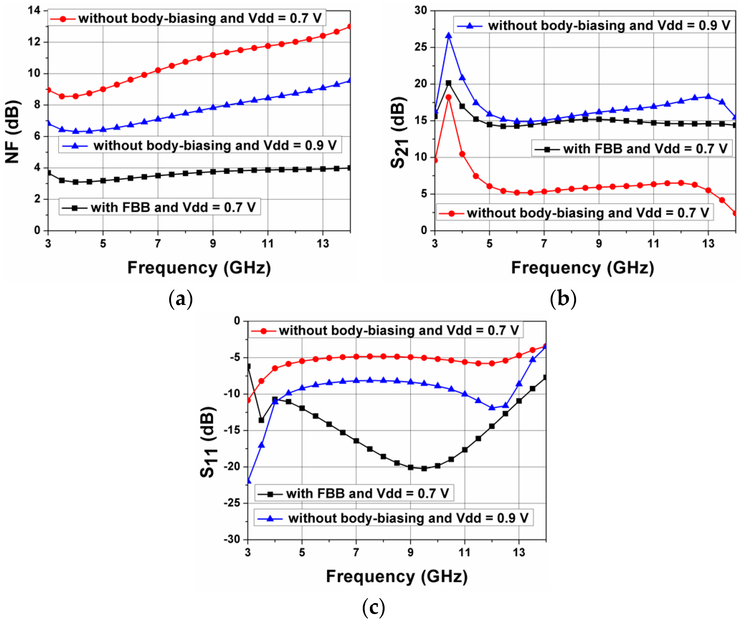
To evaluate the effect of feedback body bias technique on noise figure, power gain and input reflection coefficient, the proposed LNA has been simulated with feedback body bias at
Vdd supply of 0.7 V and without body biasing at
Vdd supply of 0.7 V and 0.9 V. It can be observed from
Figure 6 that noise figure, power gain and input matching performance of the proposed LNA was improved with a CG FBB topology with the advantage of requirement of lower
Vdd supply.
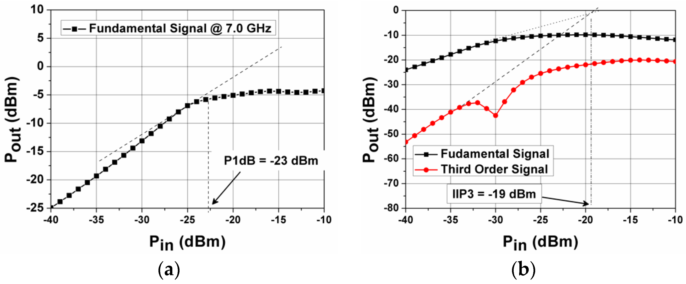
Another significant parameter to be considered is linearity. The input signal received from the antenna must be linearly amplified by the designed LNA. As LNAs are usually biased at a very low voltage, at this low voltage the linearity survives due to transconductance (
gm) and drain-conductance (
gds) nonlinearities of the MOS device. Linearity of the proposed LNA has been analyzed graphically in terms of a 1-dB compression point (
P1dB), and a third order interface point (
IIP3) for which input power was swept from −40 dBm to −10 dBm. It can be observed from
Figure 7a that
P1dB at the fundamental frequency of 7.0 GHz was −23.0 dBm. A two tone test was performed at a center frequency of 7.0 GHz that gave two tones at
f1 = 6.995 GHz and
f2 = 7.005 GHz with frequency spacing of 10 MHz to find
IIP3. Extrapolating the fundamental signal and third order signal outputs and finding out the intersection of the two gives the approximate value of
IIP3. It can be observed from
Figure 7b that
IIP3 of the proposed LNA was −19 dBm.
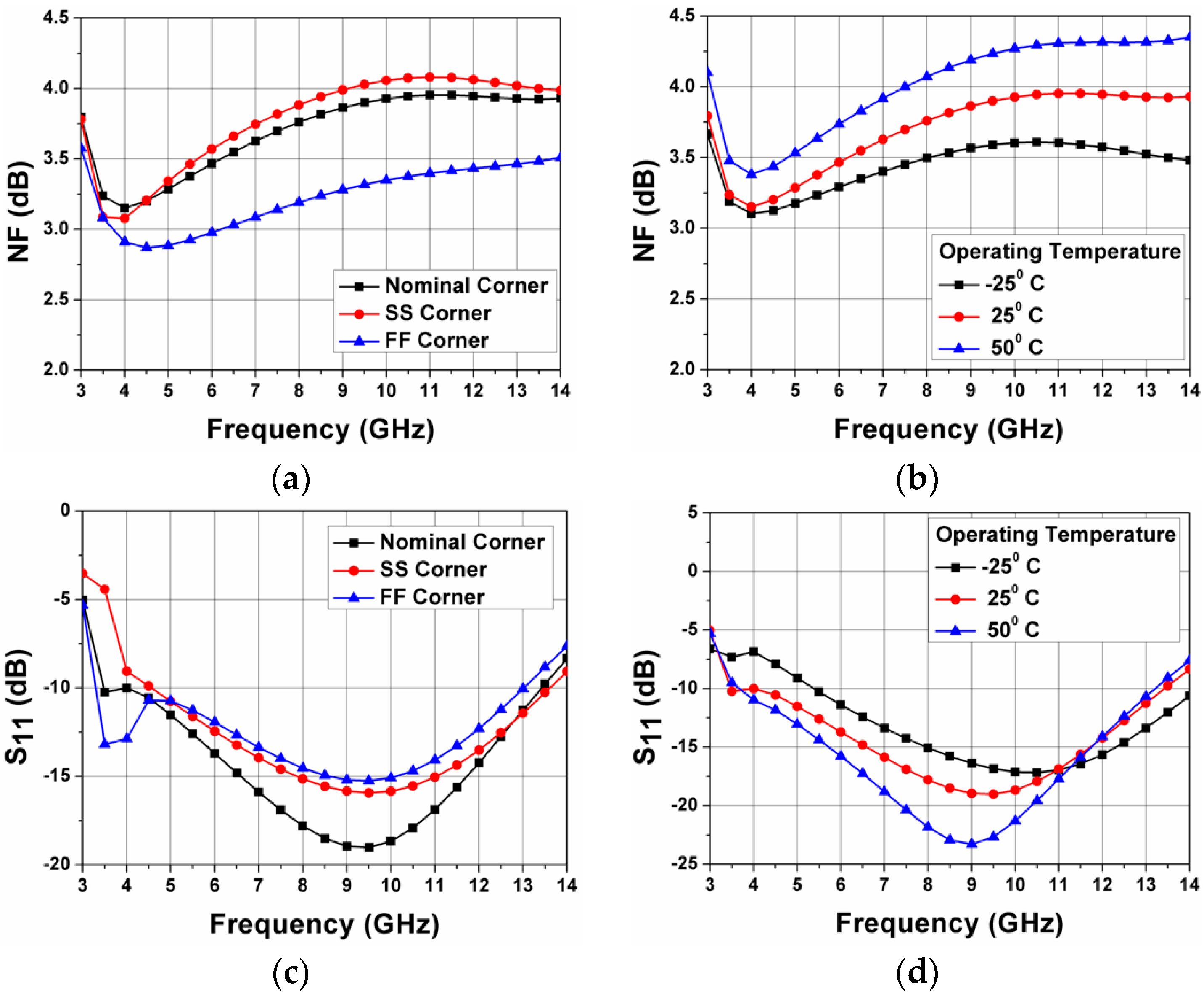
The designed UWB LNA must be stable against temperature variations. To ensure this, the designed LNA was simulated at nominal, slow-slow (SS), and fast-fast (FF) process corners and at different temperatures of −25°, 25° and 50° Celsius (
Figure 8). It can be observed from
Figure 8a,b that the feedback of the proposed UWB LNA had a minimum NF that varied from 2.87–3.75 dB to 3.0–4.0 dB at the FF and SS corners respectively, and it varied from 3.1–3.6 dB to 3.3–4.3 dB for −25 °C to −50 °C temperature variations, respectively.
Figure 8c,d shows the frequency responses of the input reflection coefficient against process and temperature variations. It can be observed that
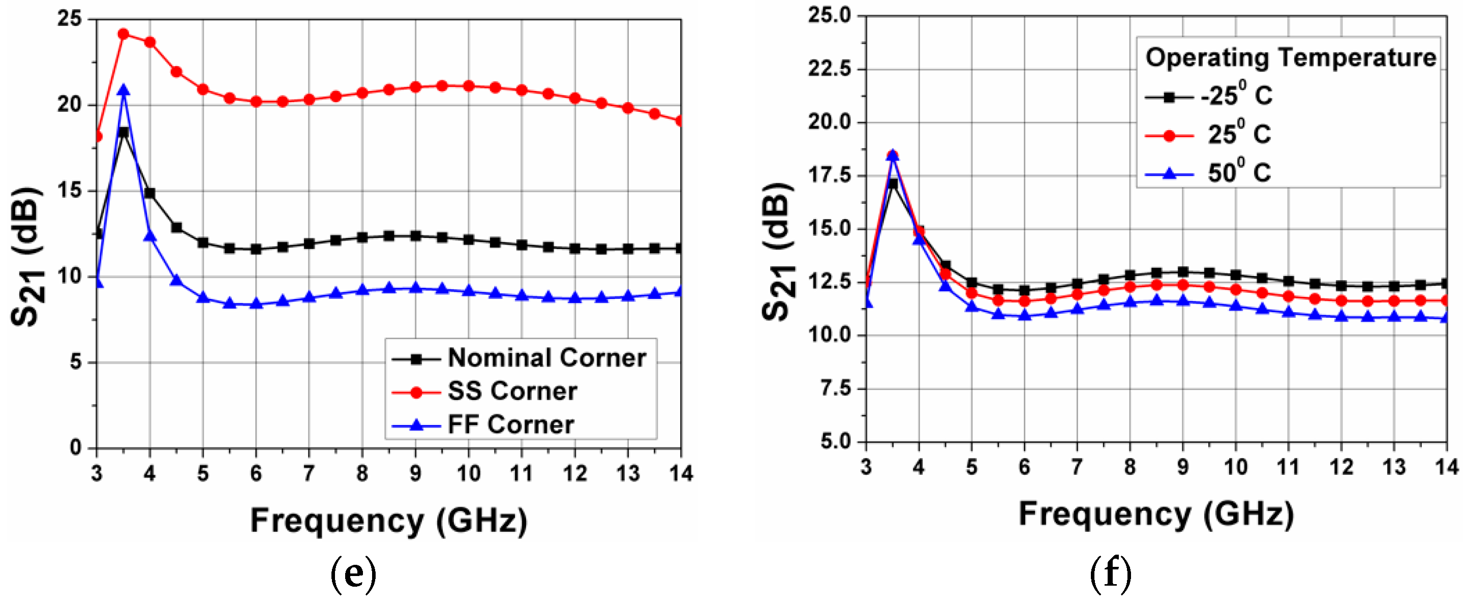
S11 was less −9.0 dB for 4–13 GHz for all process corners, and was less than 9.1 dB for 5–13 GHz for the temperature range of −25 °C to 50 °C. The power gain frequency response of the proposed LNA is shown in
Figure 8e–f, which confirmed the robustness of the proposed UWB LNA against temperature variations.
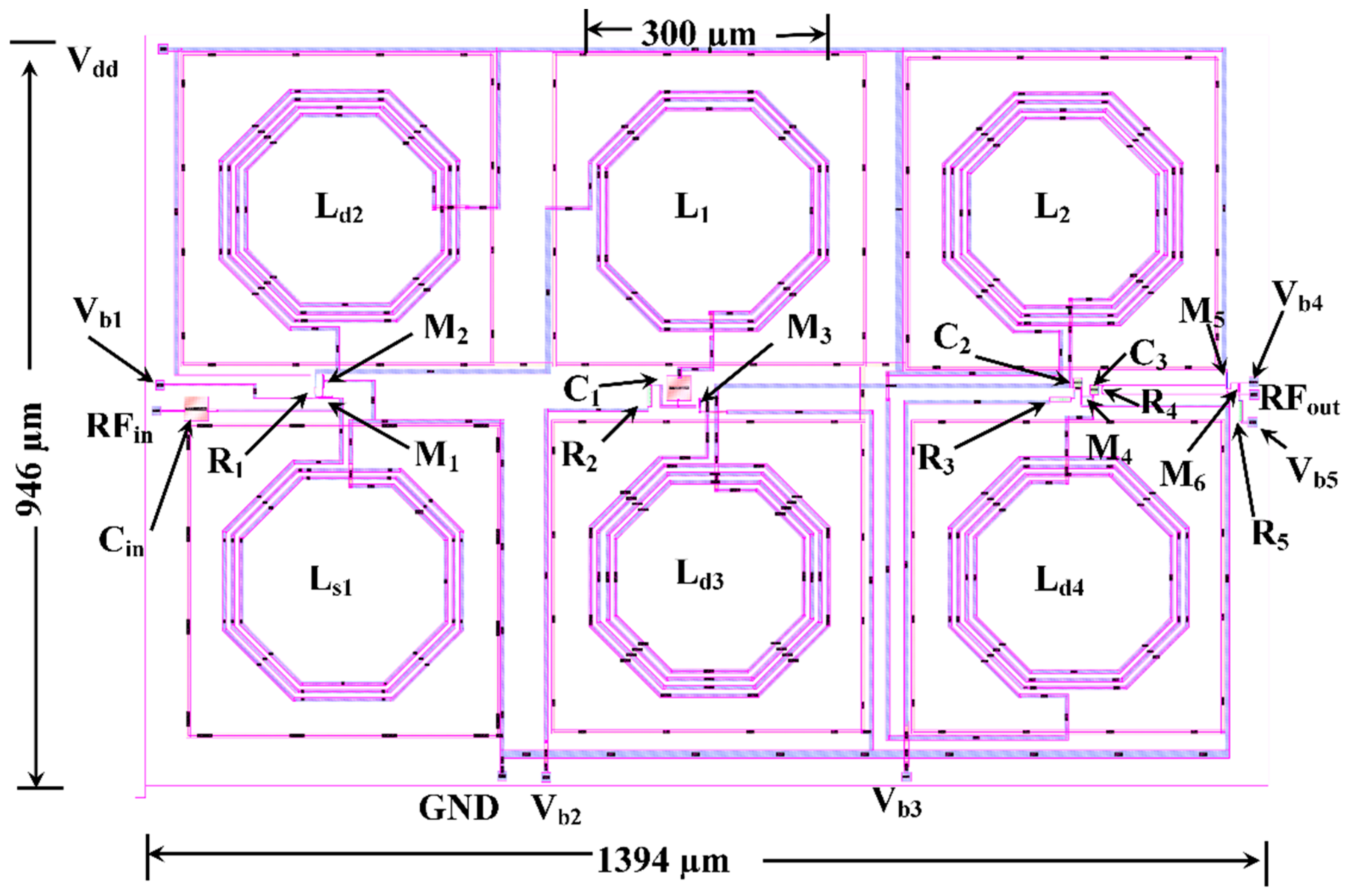
Results in this study were obtained with theoretical calculations and simulations with standard model files in 90 nm technology. The chip-layout of the proposed LNA is shown in
Figure 9, which is designed using the Cadence Layout tool using a 90 nm CMOS process. The dimensions of all the inductors have been calculated using the expression from Mohan et al. (1999) [
24]. All the inductors have been designed using metal-1 layer with a turn width and turn spacing of 5 µm and an outer diameter (
Dout) of 300 µm for each. As the designed LNA is required to achieve a large bandwidth, the Q-factor of the inductors used in the proposed LNA was very small and ranges from 0.6–1.5. The capacitors
Cin and
C1 were designed using metal-insulator-metal using metal-2 and metal-3 layers. The capacitors
C2 and
C3 were designed using a N-type MOS device, whereas the N-diffusion resistors were used to decrease the layout area. The chip layout occupied 1.318 mm
2 of area. In order to evaluate and compare the overall performance of the proposed UWB LNA with previous work, a figure-of-merit (FOM) has been evaluated. The figure-of-merit can be obtained as [
14,
22,
23]:
where |
S21|
abs is the absolute value of
S21,
BW is the 3-dB bandwidth measured in GHz,
F is noise factor and
PmW is the power consumption in mW.
The simulation results of the proposed UWB LNA were compared with the previous published work from a wide literature in
Table 2. Comparison mainly focused on noise figure (NF), input reflection coefficient (
S11), output reflection coefficient (
S22), power gain (
S21) and power consumption for 3.1–10.6 GHz UWB frequency. The LNAs implemented in References [
8,
23,
25] uses common-source resistive feedback topology for wideband input matching, but the noise figure was in 3.0–5.3 dB range and consumed more power as compared to the LNA proposed in this paper. A noise cancelling technique was utilized in References [
14,
23] with a high power consumption of 9.97 mW and 23.23 mW respectively. CS with an FBB technique was used in References [
20,
26,
27], however, the power consumed by the LNA proposed in References [
20,
26] was greater than 9 mW and 13.0 mW, respectively. Due to the use of the small power supply LNA proposed in References [
27] it consumed less power but had
S11 of ≤−5 dB. It can be observed from
Table 2 that the proposed LNA design had better overall performance in terms of the noise figure,
S11,
S21,
S22, bandwidth and the power consumption.


