Analytical Performance of the Threshold Voltage and Subthreshold Swing of CSDG MOSFET


Department of Electronic Engineering, Howard College, University of KwaZulu-Natal, Durban 4041, South Africa
*
Authors to whom correspondence should be addressed.
J. Low Power Electron. Appl. 2019, 9(1), 10; https://0-doi-org.brum.beds.ac.uk/10.3390/jlpea9010010
Submission received: 9 November 2018
/
Revised: 30 December 2018
/
Accepted: 8 January 2019
/
Published: 26 February 2019
Abstract
:In this research work, the threshold voltage and subthreshold swing of cylindrical surrounding double-gate (CSDG) MOSFET have been analyzed. These analyses are based on the analytical solution of 2D Poisson equation using evanescent-mode analysis (EMA). This EMA provides the better approach in solving the 2D Poisson equation by considering the oxide and Silicon regions as a two-dimensional problem, to produce physically consistent results with device simulation for better device performance. Unlike other models such as polynomial exponential and parabolic potential approximation (PPA) which consider the oxide and silicon as one-dimensional problem. Using the EMA, the 2D Poisson equation is decoupled into 1D Poisson equation which represent the long channel potential and 2D Laplace equation describing the impacts of short channel effects (SCEs) in the channel potential. Furthermore, the derived channel potential close-form expression is extended to determine the threshold voltage and subthreshold behavior of the proposed CSDG MOSFET device. This model has been evaluated with various device parameters such as radii Silicon film thickness, gate oxide thickness, and the channel length to analyze the behavior of the short channel effects in the proposed CSDG MOSFET. The accuracy of the derived expressions have been validated with the mathematical and numerical simulation.
1. Introduction
The downscale of the conventional MOSFETs devices to nanoscale regime has been the driving force of the semiconductor industry [1,2,3]. The main objective behind the transistor scaling is to enhance device performance, speed, low operating power, and packing density of the IC [4,5]. However, the downscaling of the device has led to problems of short channel effects (SCEs), such as threshold voltage roll-off, degradation of the subthreshold threshold swing, and subthreshold leakage current [6,7,8,9]. To overcome this problem several device structures has been proposed. Double gate structures [10,11,12] introduce the concept of volume inversion leading to higher current, better scalability, and increased conductance than conventional MOSFETs, but its use is limited based on the cost of production and process complexity.
In order to overcome these shortcomings of cost of production and process complexity, several novel geometric structures have been proposed. One of such structures is a three-dimensional cylindrical surrounding-gate (CSG) MOSFET [13,14,15,16,17]. The surrounding gate on the silicon pillar provides better coupling and its fabrication is less complex compared to DG MOSFET [18]. Additionally, CSG MOSFETs poses a better immunity to SCEs than conventional single gate MOSFETs and DG MOSFETs [19,20]. The most enhancing feature of the CSG MOSFET when compared to other novel structures, like single gate, pi gate, and double gate, is its geometric structure. This device structure increases the packing density, and most importantly leads to better controllability of the gate over the channel [17,21]. The gate control results to enhancement of the subthreshold characteristics and greater immunity to SCEs. However, in terms of current drive the CSG MOSFETs have lesser current compared with the DG MOSFET, hence, its extensive use is limited for high performance application [22]. Thus, there is need to improve on the geometric structure of the CSG MOSFET to enhance the current drive, the gate control over the channel and further improve the SCEs immunity at the nanoscale regime.
A novel structure, the cylindrical surrounding double gate (CSDG) MOSFET, was proposed by Srivastava et al. [12]. The geometry is similar to that of the CSG MOSFET with an internal core gate. The core gate enhances the channel control and improves the SCEs immunity. Additionally, the device allows for higher packing density and higher volume inversion than DG MOSFETs and CSG MOSFETs [23,24]. The explicit charge model based on the unified charge model was carried out by Srivastava et al. [25,26]. The authors analyzed the channel current for the novel structure to be higher than the single, DG MOSFET, and CSG MOSFET. However, the authors did not consider the subthreshold regime. Verma et al. [27] worked on the subthreshold regime of the CSDG MOSFET in which only the threshold voltage was analyzed.
The proposed CSDG MOSFET is designed on a hollow concentric cylindrical structure in which a simple analytical channel potential model has been derived at subthreshold regime. The 2D Poisson equation is solved with the EMA as a boundary valued problem to obtain the minimum surface potential. The minimum surface potential is further extended in the derivation of the threshold voltage model, subthreshold current, and subthreshold swing of the device structure. Its performance is investigated with the device parameters. However, we neglected the quantum mechanical effect by assuming a minimum silicon body thickness of 5 nm [28]. This paper is organized as follows: The structure of CSDG MOSFET with the boundary conditions and modelling of the minimum surface potential with EMA is presented in Section 2. The threshold voltage model for the proposed CSDG MOSFET structure is derived using the minimum surface potential in Section 3. The subthreshold swing is derived in the Section 4. The results have been discussed in the Section 5. Finally, Section 6 concludes the work and recommends future aspects.
2. Structure of CSDG MOSFET and Potential Distribution Model using EMA Model
2.1. CSDG MOSFET Structure
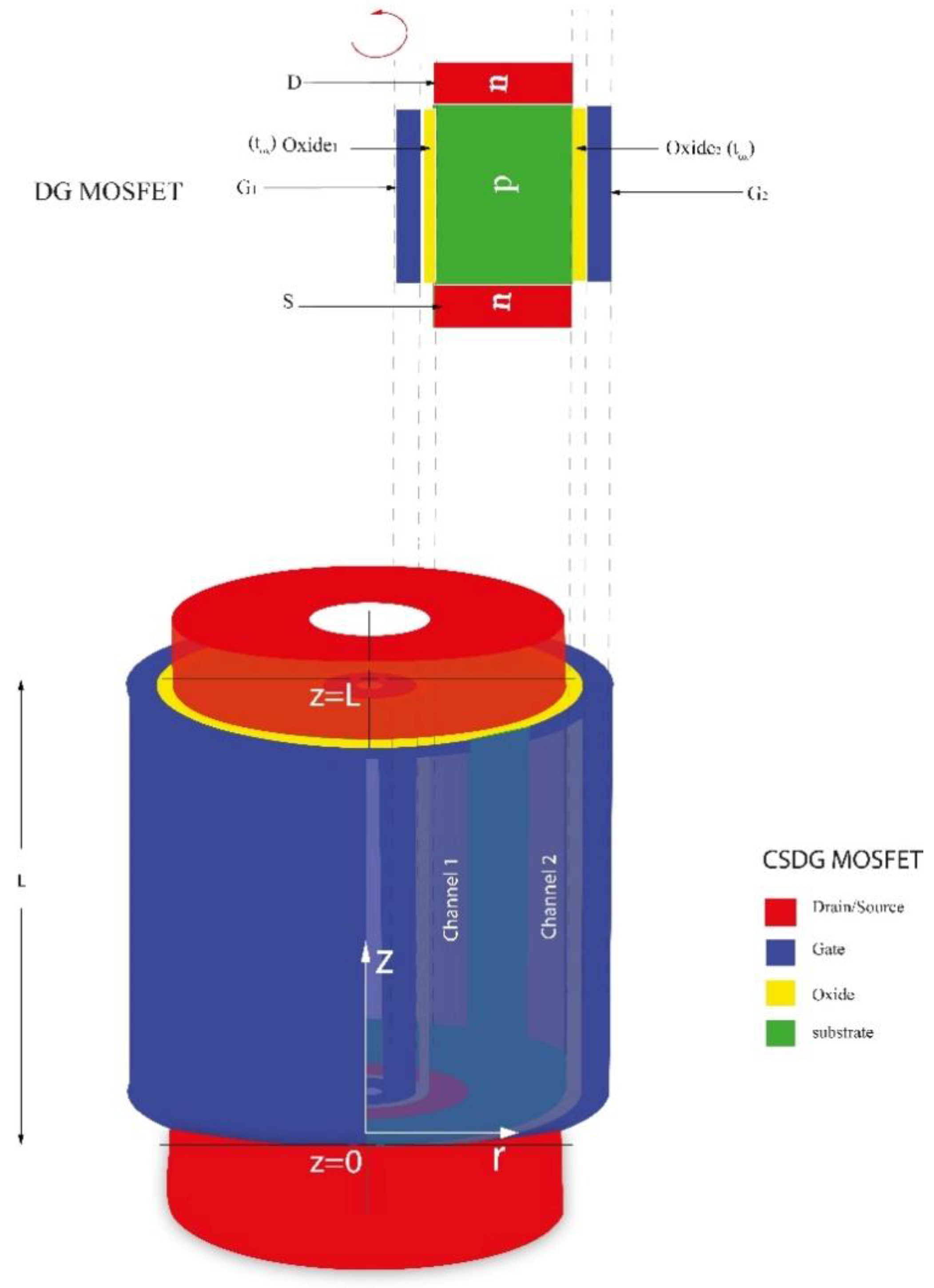
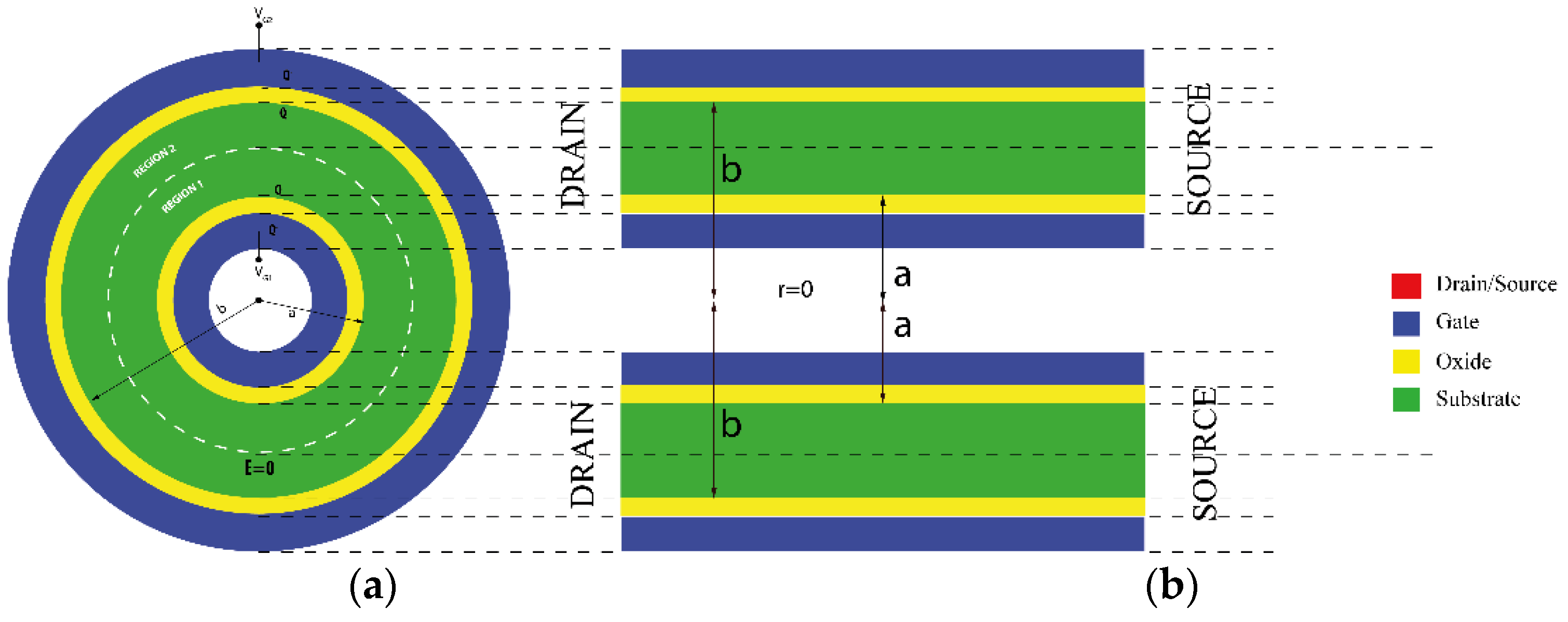
The CSDG MOSFET is an extended version of DG MOSFET and CSG MOSFET in terms of form factor and current drive, respectively. The DG MOSFET has two gates (blue color), the oxides (yellow color), the drain/source (red color) and a silicon substrate (P, green color). When this DG MOSFET is rotated with respect to the reference point, the first gate (G1) forms the internal radius (r = a) with a circular thin oxide to immune the effect of SCEs. The second gate (G2) forms the external radius (r = b) with circular thin oxide, forming a hollow concentric cylinder [29]. Between the oxides is the silicon substrate, while the extension forms the source and drain part of the cylinder as shown in the Figure 1.
The internal and external gates of the CSDG MOSFET can be biased either separately or simultaneously to form separate inversion or volume inversion, respectively. However, the simultaneous biasing of the CSDG MOSFET is usually preferred due to higher current drive (volume inversion). Assuming the gate of an n-channel CSDG MOSFET are positively biased simultaneous. Below threshold voltage, the minority carrier electrons are attracted towards the oxide-silicon interface forming weak inversion. As the biasing voltage exceeds the threshold voltage, the onset of strong inversion occurs in CSDG MOSFET in similar manner with traditional MOSFET [30]. Both biasing gates voltage forms the internal and external channel of the device structure at subthreshold region. However, above threshold voltage the two channels contribute to higher current drive know as volume inversion.
2.2. Potential Model Derivation with EMA Model
2.2.1. Evanescent Mode Analysis (EMA) Model
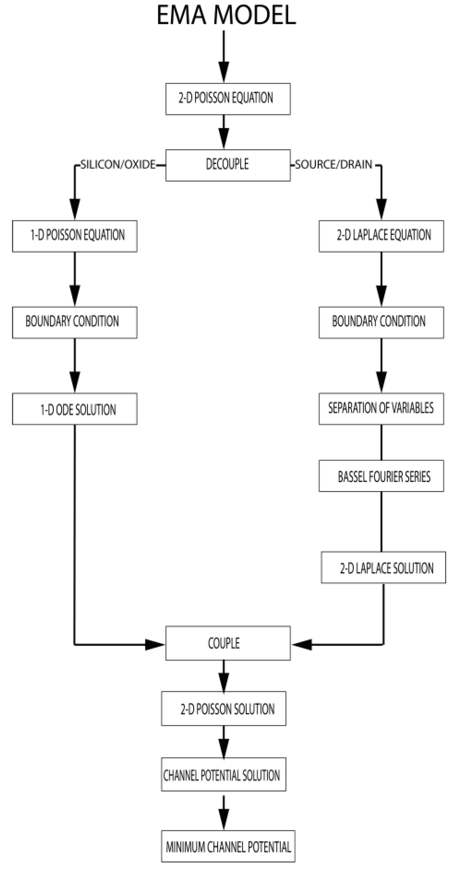
The evanescent mode analysis is a mathematical model for solving the 2D Poisson equation as a function of transverse confinement of the device structure with respect to its boundary condition [20].
The 2D Poisson solution yields the electrostatic potential distribution confinement of the CSDG MOSFET as shown in the flowchart of Figure 2. The SCEs on the CSDG MOSFETs are governed analytically by the electrostatic potential caused by biasing the inner and outer gate simultaneously. The derived potentials are extended in modelling the threshold voltage and subthreshold swing. Since, the threshold voltage roll-off are consequences of electrostatic charge sharing effect, it is typically considered as one major indicator of SCEs [31]. Another indicator of SCEs is the subthreshold swing degradation which results to higher off-state current.
2.2.2. 2D Poisson Equation
In the subthreshold (weak inversion) regime, the 2D channel potential region, ψ (r, z) is determined from cylindrical Poisson’s equation in the cylindrical coordinate system. Assuming uniform channel doping and the independency of the channel potential on the angle θ as highlighted by [14], the 2D Poisson equation (in cylindrical coordinate) is expressed as [32]:
where ψ(r, z), NA, q, and εsi, are the electrostatic potential distribution in the radii silicon film, doping concentration in radii silicon film, electric charge, and dielectric permittivity of the silicon, respectively.
The electrostatic potential, ψ(r, z) can be modeled by decoupling the 2D Poisson equation into two-part as shown in Figure 2: (i) 1D in the silicon region through the oxide thickness, and (ii) 2D based on the source and drain impact on the channel using method of separation of variables [33], that is:
where ψ1D (r) is the channel potential approximation which satisfies 1D Poisson’s equation under depletion approximation, along the silicon thickness and it is given as [34]:
Additionally, ψ2D (r, z) accommodates the 2D variation of the channel potential at the oxide-silicon interface with zero charges which satisfies the 2D Laplace equation [35]. The Laplace equation describes the impact of the source and drain on the channel potential. It is given as:
2.2.3. Boundary Condition for the CSDG MOSFET
The boundary conditions for the silicon body and gate oxide are used to solve the decoupled Poisson given Equations (3) and (4) with respect the structures in Figure 3 and Figure 4.
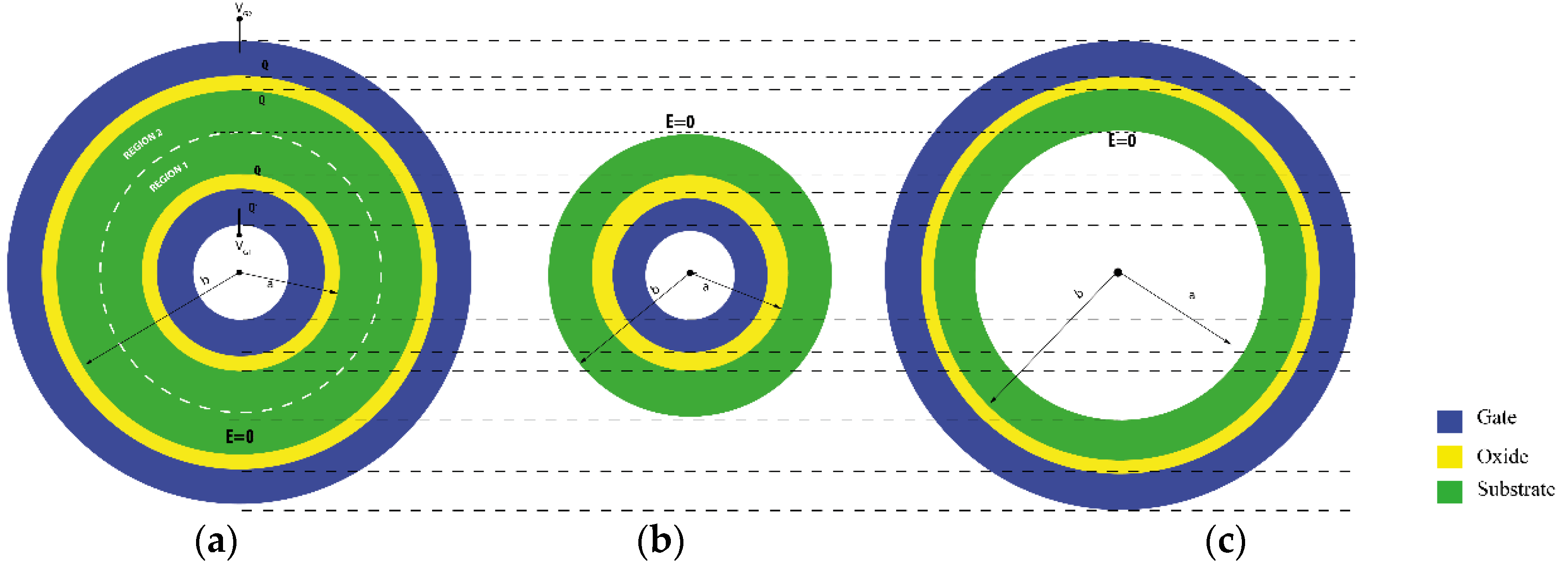
Based on Gauss’ Law [36], zero electric field must exist within the center of the silicon subtract region indicated by the circular dash line known as the Gaussian surface in Figure 4a and Figure 5a. The CSDG MOSFET is an advanced version of double-gate MOSFET as shown in Figure 1 and Figure 3. It can also be treated as CSG MOSFET since the total electric field beyond E = 0 does not have effect on the enclosed surface within the circular dash line and likewise the electric field at the hollow center is zero assuming no charge exist in the center [37]. Hence, the internal and the external radius of CSDG MOSFET can be treated separately as two CSG MOSFET as shown in Figure 4.
In order to obtain the boundary condition for the CSDG MOSFET, Figure 3 and Figure 4 are considered as follows:
(I) The potential at the gate surface for internal and external gates respectively are obtained as:
Potential at the center of silicon for the internal and external gates respectively with respect to the hollow structure:
- (II)
- The electric field at the channel center for internal and external potential, respectively:
- (III)
- The electric field at the silicon-oxide interface for internal and external potential, respectively:
- (IV)
- The internal electrostatic field boundary condition based on 1D Poisson equation:where:
- (V)
- The external electrostatic field boundary condition based on 1D Poisson equation:where:
- (VI)
- The boundary condition along the Z-direction can be used to solve the 2D Laplace equation at the source and drain end. Therefore, the Potential at the source end where (Z = 0) is given as:
Potential at the drain end (Z = L) is given as:
By substituting Equation (13) into Equation (2), we obtained:
where Vbi, VFB, VGS, and VDS, are the built-in voltage, flat band voltage, gate to source voltage, and drain voltage, respectively. Cox1 and Cox2 are internal gate and external gate oxide capacitance, respectively, and εsi and εox are dielectric permittivity of silicon and the dielectric permittivity of the oxide. Additionally, r varies to a when considering the internal potential and to b when considering the external potential in Equations (9) and (11), respectively.
Using the boundary conditions Equations (4)–(14), the surface potential for the internal and external gate of the proposed CSDG structure is (Appendix A contains the detailed procedure):
The surface potential obtained in Equations (15) and (16) is extended in the modelling of the threshold voltage and subthreshold swing of the proposed CSDG MOSFET which predicts the device characteristics and performance.
3. Threshold Voltage Model for the Proposed CSDG
The CSDG MOSFET as a switch requires an external source to be able to determine the On-OFF nature of the device. Since MOSFET are voltage-controlled device, a DC voltage is required to control the CSDG MOSFET. This DC voltage required for the ON—switching of the device when a reasonable drain current is achieved is known as the threshold voltage.
Threshold voltage can also be defined as the gate voltage at which the minimum surface potential is twice the Fermi potential, 2ϕf [38]. Hence, Equations (2), (15), and (16) is simplified further by setting its first derivative at z = 0 along the z-axis to obtain the minimum surface potential position (zmin) which equates the Fermi potential level of the device structure. After mathematical transformation, the minimum surface potential in terms of zmin is given as:
where:
where ni is the intrinsic carrier concentration, r = a for internal cylinder and r = b for external cylinder, and m = 0 and m = 1 for the internal and external coefficient. K, T, q, NA, and ni are the Boltzmann’s constant, Temperature (K), electronic charge, and doping concentration, respectively.
The threshold voltage for the proposed CSDG structure is given as:
where VTHL_CSDG are the threshold voltage for the long channel assuming the drain and source has no the effect on the channel, VTHi_CSDG are the threshold voltage roll-off due to drain and source effects with respect to internal or external gate, and VTHsi_CSDG is the short channel threshold voltage for the internal and external gate surface potential.
Considering the Long channel condition and assuming gradual channel approximation [39], the threshold voltage for the internal and external gates are given based on Equation (17) as:
Considering the short channel condition, we included the drain and source effect in the model based on Equation (17) as given:
(a) Considering the internal gate (r = a) for the short channel model:
From Equation (17) we obtain:
This can be expressed in polynomial form of second order as given:
where:
Therefore, the threshold voltage for the internal gate surface potential due to the short channel is given as:
Hence the closed-form expression of the threshold voltage roll-off for the internal gate of CSDG MOSFET is given with the practical assumption of λnL >> 1 [40]:
(b) Considering the External gate (r = b) for the short channel model:
Similarly, this can be expressed as a quadratic equation as given:
where:
Therefore, the threshold voltage for the short channel is:
Like the closed-form expression of the short channel threshold voltage for the external gate of CSDG MOSFET is given as:
Therefore, the threshold voltage of the short channel can be determined either through the internal gate minimum surface potential or the external gate minimum surface potential of the CSDG MOSFET as given in Equations (27) and (32).
4. Subthreshold Current and Subthreshold Swing
This section presents the subthreshold current and the subthreshold swing close-form expression using the minimum surface potential derived from Equation (17). Subthreshold swing determines the device’s behavior by showing the effect of the change in external gate voltage on the subthreshold current. In an ideal MOSFET, the subthreshold current is zero when the applied gate voltage is lesser than threshold voltage. However, in the practical aspect, such behavior is never obtainable. The ideal subthreshold swing value at room temperature is 60 mV/dec. Furthermore, the analyses are verified with the numerical simulation.
4.1. Subthreshold Current
The subthreshold current flows from source to drain along the channel length through diffusion mechanism. Hence, the subthreshold current is given by integration with respect to the circular area as given [41]:
where nm is the electron density at subthreshold regime in relation to classical Boltzmann’s equation. it is given as:
Dn, VT, and ni are the diffusion constant, thermal voltage, and intrinsic concentration respectively. Using the Equation (33), assuming the subthreshold current occurs at the virtual cathode (z = zmin), the subthreshold current of CSDG MOSFT (I_CSDG) is obtained by:
where:
M(z) and N(z) can be obtained by integrating the indefinite fa(r) and fb(r) through the trapezoidal rule of numerical approach as given by [40]:
By equating the partition number to one (n = 1) in Equations (37a) and (37b), the subthreshold current for CSDG MOSFET can be obtained in Equation (35b).
4.2. Subthreshold Swing
Subthreshold swing (SS) is defined as the change in gate bias voltage required for a change of one decade of subthreshold drain current [42]. Since, subthreshold swing is an important device parameter to represents the switching characteristics of MOS device, Hence, its evaluation is a necessity and it is given as [43]:
By substituting Equation (35b) into Equation (38), the subthreshold swing can be calculated, since the ψ (r, zmin) is a function of change in voltage (dv) from Equation (38) and dV is a function of gate voltage. However, the subthreshold swing is very difficult to obtain using the subthreshold current due to its complicated dependency of the minimum radius (rmin) on the gate voltage and the numerical integration involved. In a simpler approach, the subthreshold current can be related to the minimum surface potential, ψs_min(r, zmin) through the electron concentration at the virtual cathode [44]. This is because at subthreshold operation, the subthreshold current is dominated by a diffusion process. This leads to a probability of mobile electron surmounting the source end of the energy barrier. Thus, it can be assumed that the subthreshold current is proportional to the carrier concentration at the virtual cathode nmin (r, zmin), given as [42]:
Since the electron density follows Boltzmann distribution according [45] we can express the SS by substituting Equation (39) in Equation (38) as given:
where .
From Equation (39) minimum surface potential can be obtained as:
Therefore, the subthreshold swing can be obtained using Equations (40), (42), and (43). The simulation results of the close form expression obtained and the numerical results are explained in the further sections.
5. Results and Discussions
In this section, the theoretical and numerical simulation results are presented using Equations (27), (32), (35), and (40). The list of parameters used for the CSDG MOSFETs are given in Table 1.
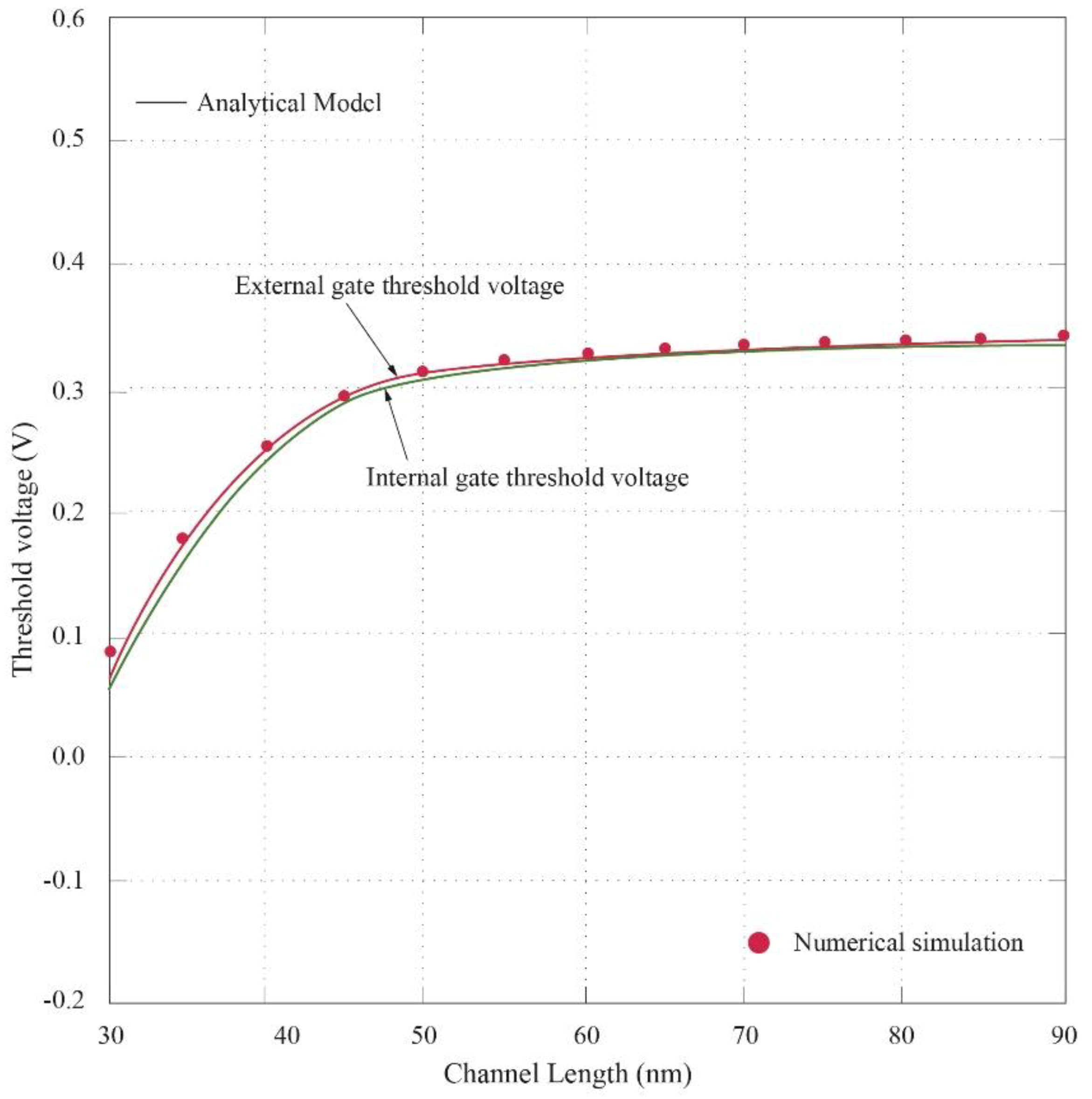
The threshold voltage of the internal and external gate CSDG MOSFET with variation of channel length is shown in Figure 5. It has been observed that the decrease in channel length, causes a corresponding rapid decrease in the threshold voltage. The phenomenon is called the threshold roll-off which can be determined with either the internal gate or external gate model. Although, the threshold voltage between the internal and external gate are almost the same. However, the external gate has lightly higher threshold voltage than the internal gate due to higher minimum surface potential as shown in Figure 5. The external gate is in perfect match with the numerical simulation.
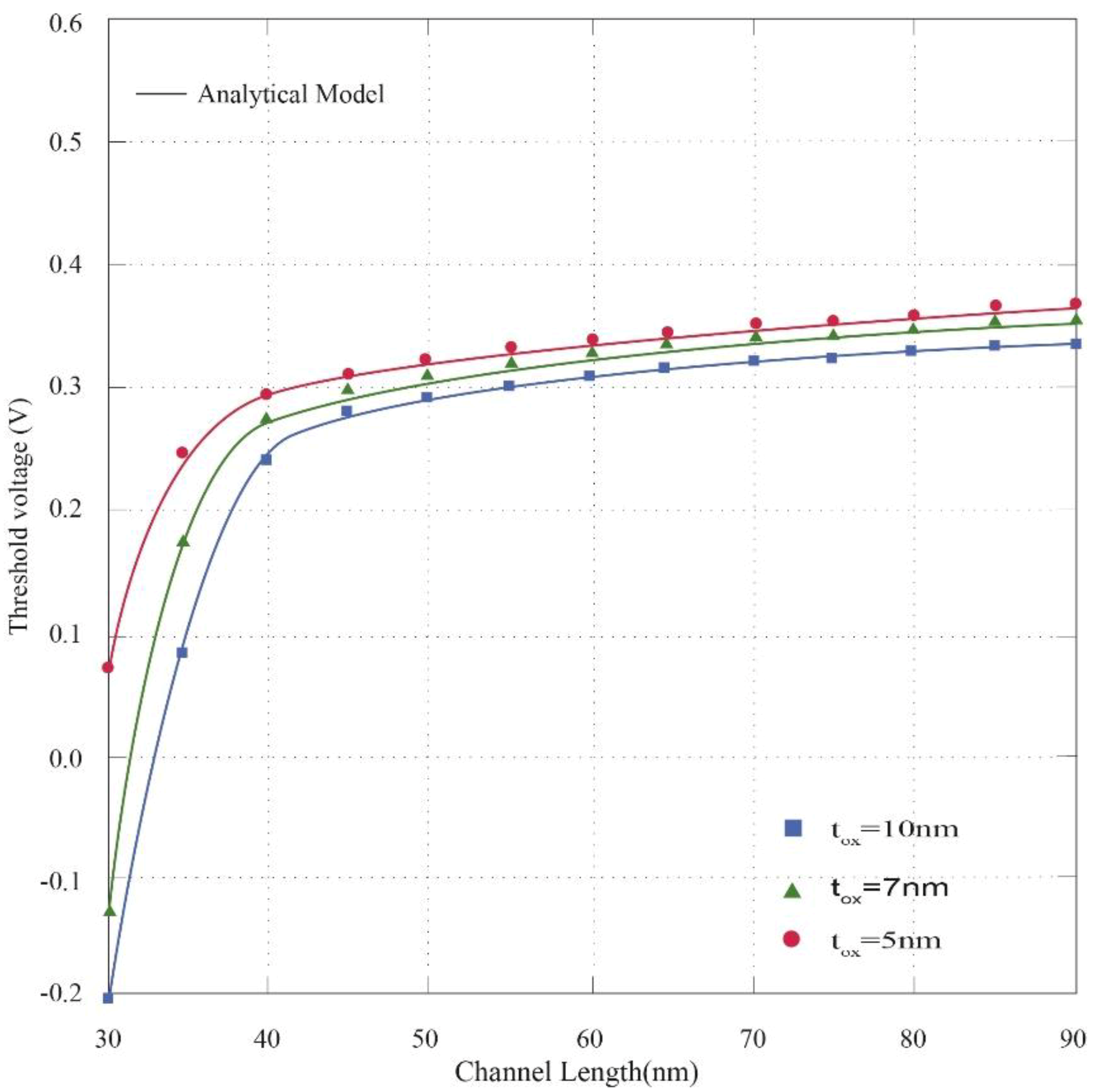
The thin gate oxide of the internal and external structure of the CSDG MOSFET enables the dominance of the vertical electrical fields over the lateral electric field resulting from the drain and source ends. This enables the two gates to have better control of the channels created within the structure. Furthermore, the dominance of the vertical electric field will result to less leakage of current when the device is turned off. The variation of threshold voltage with channel length at different oxide thickness is shown in Figure 6. It is clearly observed that the decrease in channel length, results to the decrease in threshold voltage which affects the device performance. Additionally, the lower the threshold voltage, the more unpredictable the device switching performance. This degrades the switching characteristics of the device during the turn-OFF stage. However, higher threshold voltage enhances stability and accurate switching of the device. We optimized the threshold voltage with different oxide thickness. The threshold voltage increases with decrease in gate oxide, hence, thin gate oxide tends to provide better gate controllability than the thicker oxide. Additionally, thin gate oxide reduces SCEs in CSDG MOSFETs. The result is in good agreement with the numerical simulation of the proposed structure.
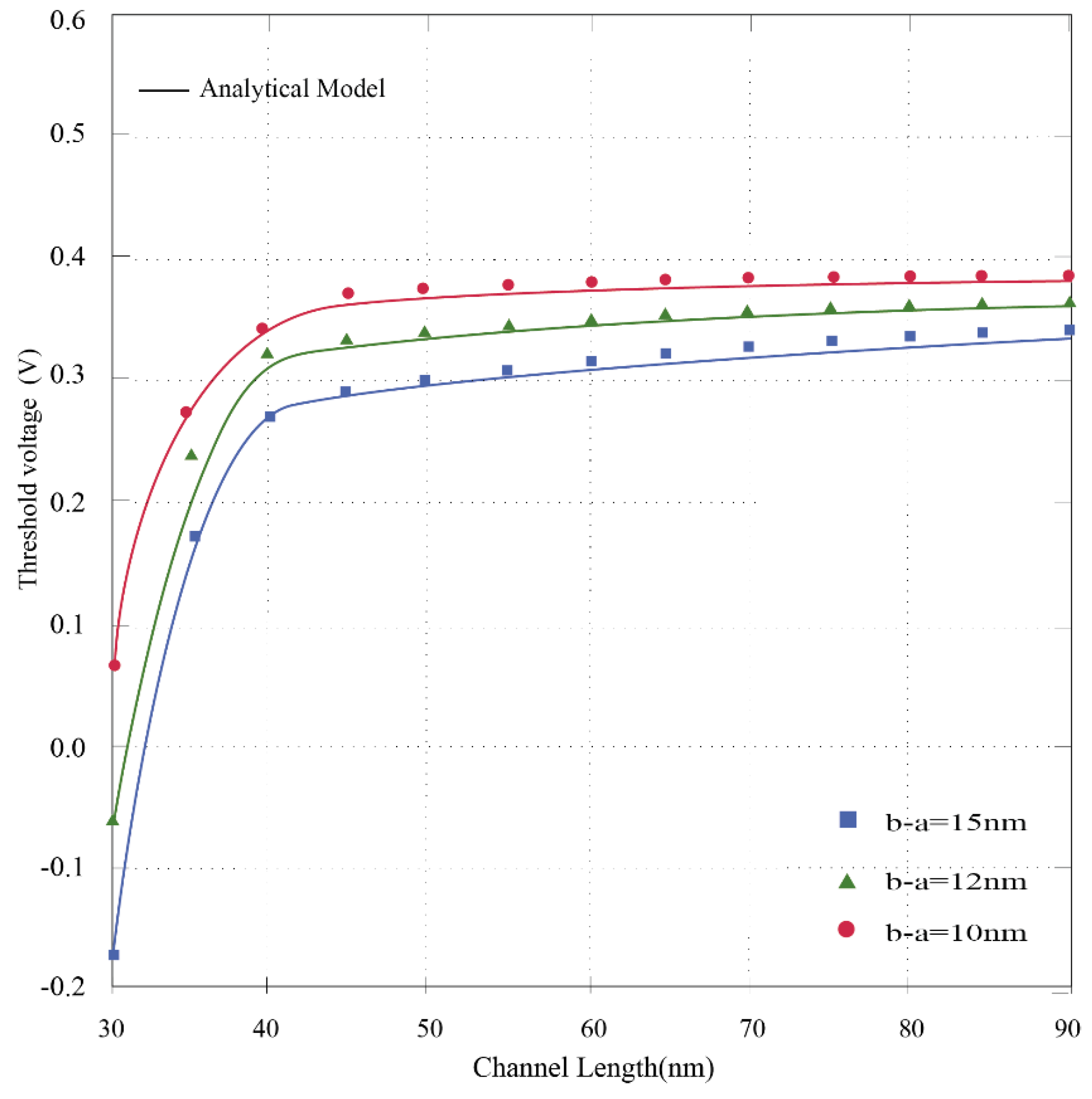
Furthermore, the thinner radii silicon film difference of the CSDG MOSFET structure enhances the internal and external gate controls of the channel carriers over the drain and source ends. The reduction in radii difference further reduces the drain and source sizes, and their impact on the channel is significantly reduced. Hence, the gates have better control of the channel carriers. The variation of threshold voltage with channel length at different radii silicon film thickness is shown in Figure 7. It is observed that as the silicon film thickness decreases, the threshold voltage of CSDG MOSFET increases because the drain ends losses control of the channel. As a result, the thin silicon film provides better gate controllability leading to low threshold voltage degradation and better suppression of SCEs. The result matches the numerical simulation of the proposed structure.
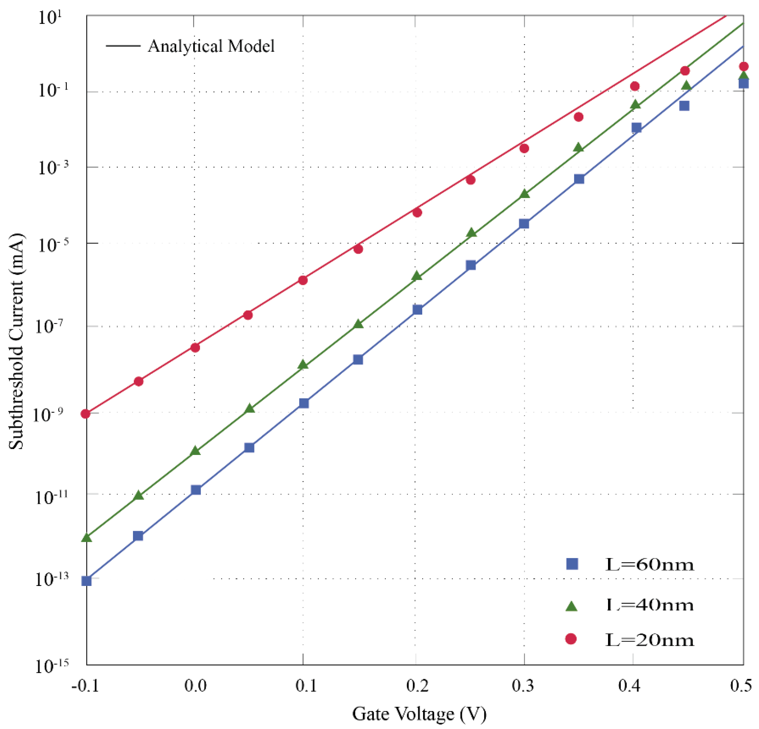
The CSDG MOSFETs provides higher drain current due to the coupled internal and external gates. These gates increase the average electric field of the structure. This enables rapid acceleration of carriers at the interface towards the drain terminal, resulting to the enhancement of the carrier transportation efficiency for the proposed structure. However, an increase in the drain current causes slight increase in the subthreshold leakage current, which needs to be minimized at less than 30 nm gate length. The subthreshold current versus the gate voltage with different variation in channel length is shown in Figure 8. The channel length is varied from 60 nm to 20 nm. It is clearly observed that the subthreshold current increases as the channel length decreases with an upward shift as clearly observed. This implies lesser control of the gate over the channel at lower channel length resulting to more leakage current. It is should be noted that the model is considered at the subthreshold regime. The slight deviation of the numerical simulation from model towards 0.5 V of the gate voltage shows the inversion onset phase. The model matches with the numerical simulation for the proposed structure within the subthreshold regime.
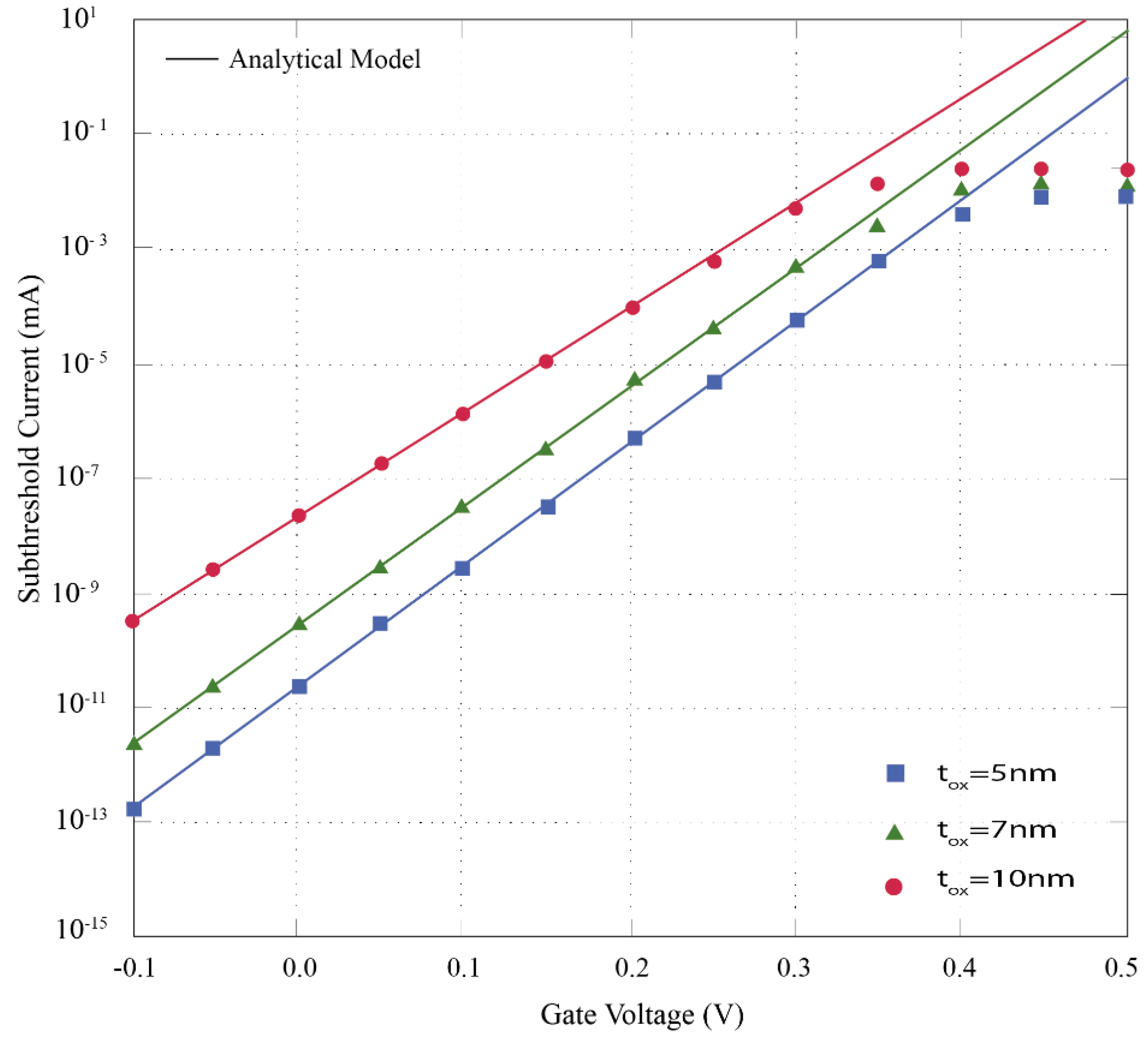
Furthermore, the presence of the thin gate oxide on the proposed CSDG MOSFET reduces the subthreshold leakage current by enabling greater gate control over the channel and minimal lateral Electric Field effects. The subthreshold current versus the gate voltage with respect to different variation of the gate oxide thickness is shown in Figure 9. It is observed that the as the gate-oxide thickness increases, the subthreshold current leakage also increases. The increased gate oxide reduces the gate control over the channel and the leakage due to impacts from the drain is added to the channel. Hence, the thin oxide is preferred over thicker oxide. However, a balance must be maintained to prevent gate-tunneling. The deviation of the numerical simulation toward 0.5 V shows the onset of the strong inversion. The numerical simulation is in good agreement with the model within the subthreshold regime.
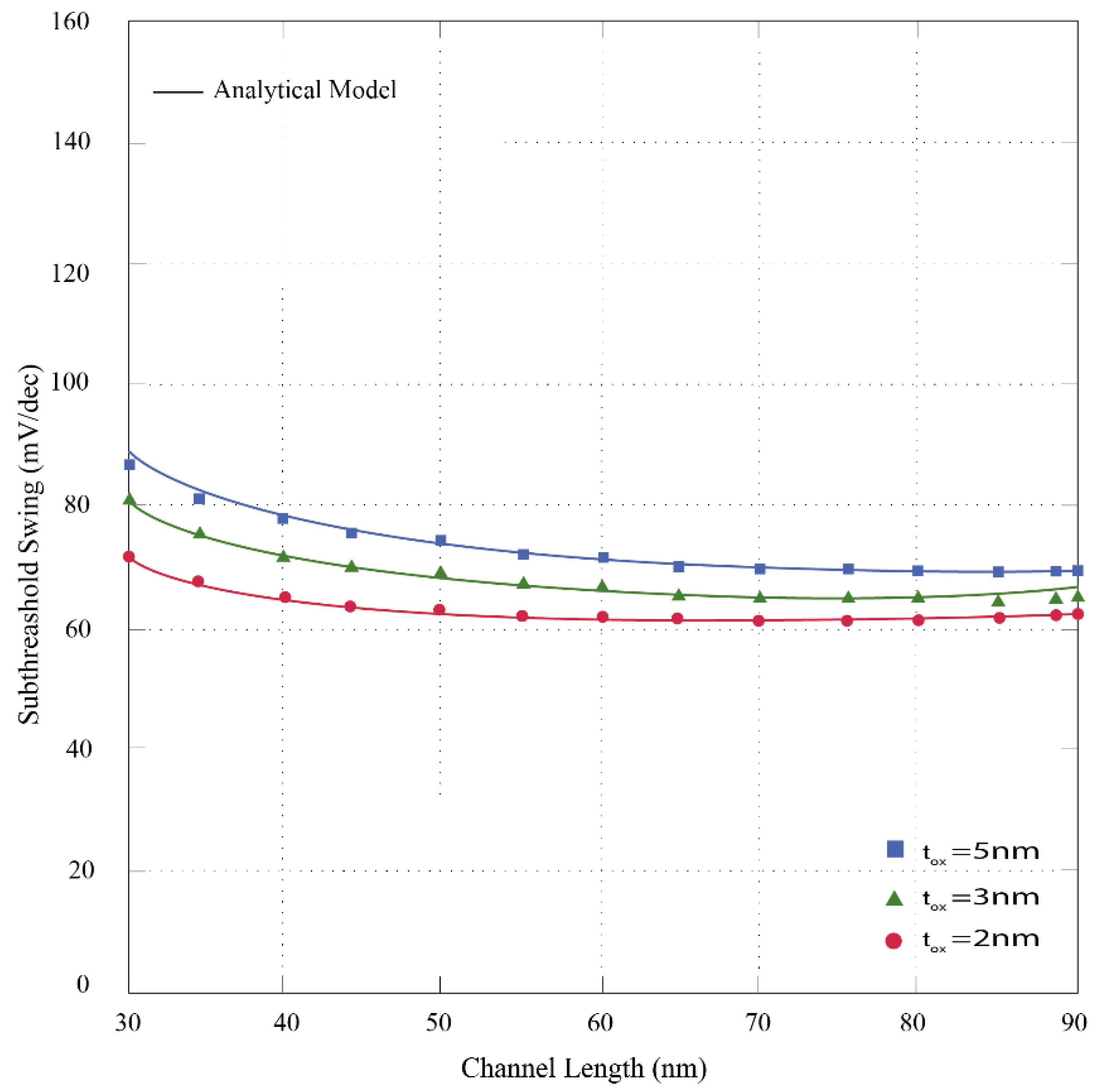
Additionally, the internal and external gates voltage describes the exponential behavior of the current in the CSDG MOSFET at subthreshold. This exponential behavior known as the subthreshold swing which increases at shorter gate lengths is minimized in CSDG MOSFET with thin oxide thickness. The smaller subthreshold swing enables better channel control by the gates at micro power application. The subthreshold swing versus channel length for different oxide thickness is presented in Figure 10. Subthreshold swing decreases significantly as the oxide thickness decreases because the gates enhances effective channel control. Hence, a thin oxide thickness provides excellent immunity over SCEs. Furthermore, the model matches the numerical simulation of the proposed structure.
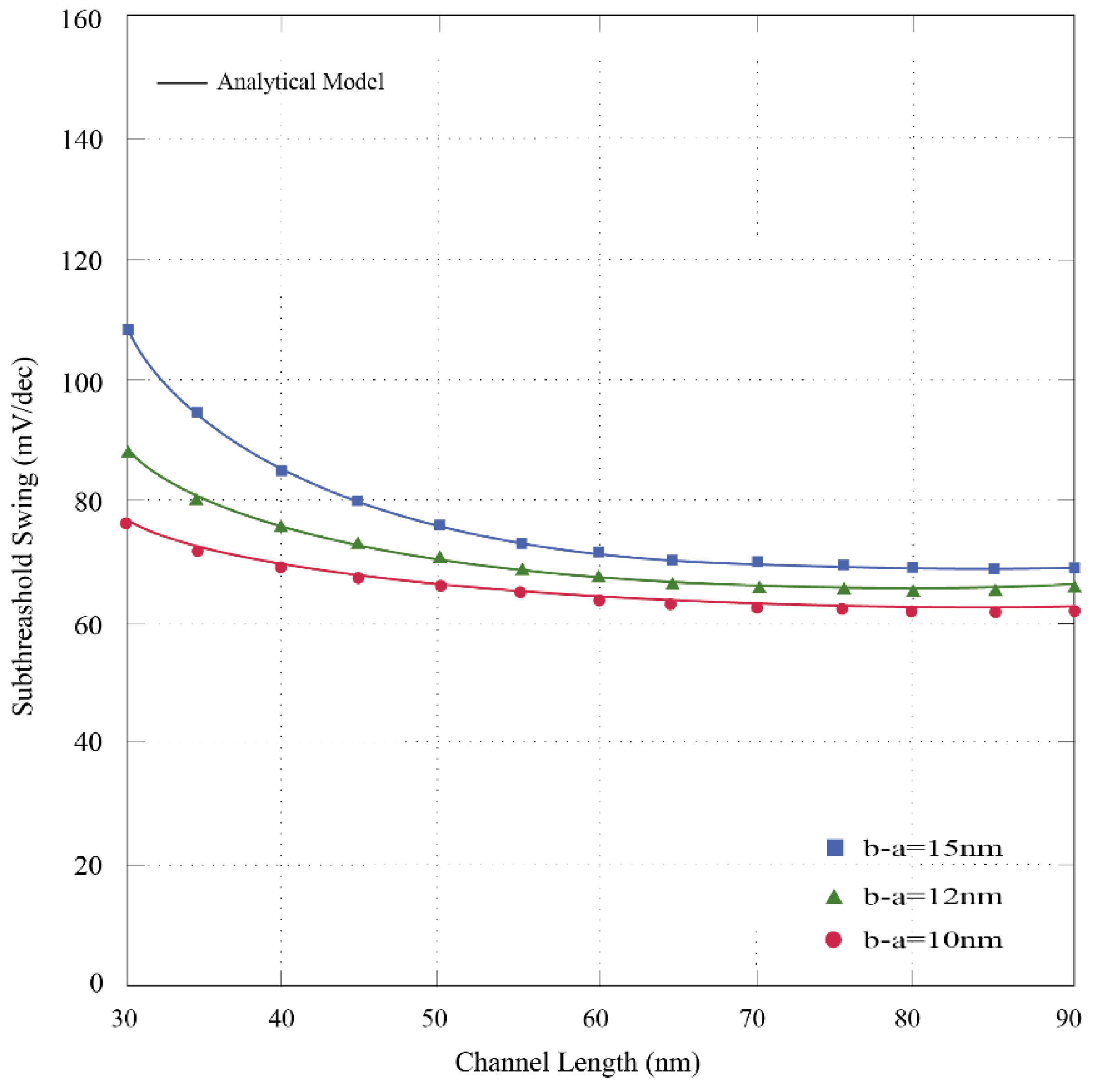
Furthermore, the reduction in radii Silicon film difference of the CSDG MOSFET enhances the device performance. The subthreshold swing has been minimized by thin radii silicon film. The internal and external gate control over the channel minimizes the lateral field effects from drain end. This results to increase in the threshold voltage. Since the subthreshold swing depends on the gate voltage, increasing the threshold voltage leads to gradual reduction in the subthreshold swing. The subthreshold swing versus channel length at various silicon film thickness is shown in Figure 11. It is obviously seen that as the channel length decrease, the subthreshold swing increases which is a major problem in scaling at nanometer. This affects the switching characteristics of the of device structure. However, as the radii silicon film thickness decreases, the subthreshold swing decreases. At 10 nm radii silicon film thickness, the subthreshold swing decreases below 80 mV/dec., enabling faster switching characteristics of the device structure. Hence, thin radii silicon film thickness helps in SCEs suppression at reduced channel length. The numerical simulation matches perfectly with the proposed device model.
6. Conclusions and Recommendations
In this research work, the close form expression for the threshold voltage, subthreshold current, and the subthreshold swing has been derived using evanescent-mode analysis to demonstrate the performance of the CSDG MOSFET. The behavior of the SCEs with various device parameters like radii silicon film thickness, gate-oxide thickness, and the channel length has been considered to predict the device performance. Results shows that the threshold voltage decreases with decrease in channel length. This results to threshold voltage roll-off which is due to 2D field effect that originated from the source and drain region because of their proximity to the channel at nanoscale length. However, this is optimized by decreasing the oxide thickness and radii silicon film difference of the CSDG MOSFET to increase the stability of the threshold voltage and better control of the turn-OFF current. This shows that the CSDG MOSFET improves immunity to SCEs, making it a promising device for the future nanometer MOSFET applications.
Although, the subthreshold swing increases above 60 mV/dec at room temperature as the channel length decreases. However, it decreases with proportional decrease in radii silicon film thickness or gate-oxide thickness which enhances the switching performance of the device for CMOS technology application. Additionally, it is observed that the decrease in the device channel length increases the subthreshold current leakage. However, the coupling of the internal and external gate control over the channel limits the leakage. Hence, making CSDG MOSFET, a suitable device for nanoscale switching operation.
Author Contributions
Conceptualization, U.A.M. and V.M.S.; methodology, U.A.M.; software, U.A.M.; validation, U.A.M. and V.M.S.; formal analysis, U.A.M. and V.M.S.; investigation, U.A.M.; resources, U.A.M. and V.M.S.; data curation, U.A.M.; writing—original draft preparation, U.A.M.; writing—review and editing, U.A.M. and V.M.S.; visualization, U.A.M.; supervision, V.M.S.; project administration, U.A.M.; funding acquisition, NOT APPLICABLE.
Funding
This research received no external funding.
Conflicts of Interest
The authors declare no conflict of interest.
Appendix A
(a) Solution to the 1-D Poisson Equation (ψ1D (r)) which satisfies the long channel potential distribution of the device structure.
The 1D equation can easily been solved with this approximation with the boundary conditions as given [13]:
- (I)
- Internal Gate potential distribution can be derived by substituting Equations (8) and (13) into Equation (A1) as given:
- (II)
- External Gate potential distribution can be derived by substituting Equations (10) and (11) into Equation (A1) as given:
(b) Solution to the 2D Laplace equation (ψ2D (r, z)) satisfies the impact of the drain and the source on the channel at nanometer length.
Authors have solved 2D Laplace equation (Equation (3b)) using the method of separation of variables as given [33]:
Considering the internal gate where (0 ≤ r ≤ a), and substituting (A4) into (3b) results to the separation of the 2D Laplace equation into two independent variables as given:
Rearranging by using a separation constant, λ known as the eigenvalue, (A5) can be separated into two parts as:
and:
Since the lowest value (n = 0) dominates the whole series due to rapid decay of higher value [47], (A8) is reduced to:
A0 and B0 are obtained using the boundary condition in Equations (12) and (13) as given:
where the eigenvalue, λ which is the scaling length parameter must verify the Poison equation at the silicon-insulator interfaces for continuity as given [48]:
Using Equations (2), (A2), (A9), and (A10), the solution for the surface channel potential in Equation (15) is derived. Using similar approach, Equation (16) is obtained.
References
- Chan, T.Y.; Chen, J.; Ko, P.K.; Hu, C. The impact of gate-induced drain leakage current on MOSFET scaling. In Proceedings of the 1987 International Electron Devices Meeting, Washington, DC, USA, 6–9 December 1987; pp. 718–721. [Google Scholar]
- Ferry, D.K.; Akers, L.A. Scaling theory in modern VLSI. IEEE Circuits Devices Mag. 1997, 13, 41–44. [Google Scholar] [CrossRef]
- Nowak, E.J. Maintaining the benefits of CMOS scaling when scaling bogs down. IBM J. Res. Dev. 2002, 46, 169–180. [Google Scholar] [CrossRef]
- Lu, W.-Y.; Taur, Y. On the scaling limit of ultrathin SOI MOSFETs. IEEE Trans. Electron Devices 2006, 53, 1137–1141. [Google Scholar]
- Momose, H.S.; Nakamura, S.I.; Ohguro, T.; Yoshitomi, T.; Morifuji, E.; Morimoto, T.; Katsumata, Y.; Iwai, H. Uniformity and reliability of 1.5 nm direct tunneling gate oxide MOSFETs. In Proceedings of the 1997 Symposium on VLSI Technology, Kyoto, Japan, 10–12 June 1997; pp. 15–16. [Google Scholar]
- Veeraraghavan, S.; Fossum, J.G. Short-channel effects in SOI MOSFETs. IEEE Trans. Electron Devices 1989, 36, 522–528. [Google Scholar] [CrossRef]
- Young, K.K. Short-channel effect in fully depleted SOI MOSFETs. IEEE Trans. Electron Devices 1989, 36, 399–402. [Google Scholar] [CrossRef]
- Suzuki, K.; Tosaka, Y.; Sugii, T. Analytical threshold voltage model for short channel double-gate SOI MOSFETs. IEEE Trans. Electron Devices 1996, 43, 1166–1168. [Google Scholar] [CrossRef]
- Monroe, D.; Hergenrother, J.M. Evanescent-mode analysis of short-channel effects in fully depleted SOI and related MOSFETs. In Proceedings of the 1998 IEEE International SOI Conference Proceedings (Cat No.98CH36199), Stuart, FL, USA, 5–8 October 1998; pp. 157–158. [Google Scholar]
- Francis, P.; Terao, A.; Flandre, D.; Van de Wiele, F. Modeling of ultrathin double-gate nMOS/SOI transistors. IEEE Trans. Electron Devices 1994, 41, 715–720. [Google Scholar] [CrossRef]
- Barin, N.; Braccioli, M.; Fiegna, C.; Sangiorgi, E. Analysis of scaling strategies for sub-30 nm double-gate SOI N-MOSFETs. IEEE Trans. Nanotechnol. 2007, 6, 421–430. [Google Scholar] [CrossRef]
- Srivastava, V.M.; Yadav, K.S.; Singh, G. Design and performance analysis of cylindrical surrounding double-gate MOSFET for RF switch. Microelectron. J. 2011, 42, 1124–1135. [Google Scholar] [CrossRef]
- Chen, Q.; Agrawal, B.; Meindl, J.D. A comprehensive analytical subthreshold swing (S) model for double-gate MOSFETs. IEEE Trans. Electron Devices 2002, 49, 1086–1090. [Google Scholar] [CrossRef]
- Chiang, T.K. A new quasi-2-D threshold voltage model for short-channel junctionless cylindrical surrounding gate (JLCSG) MOSFETs. IEEE Trans. Electron Devices 2012, 59, 3127–3129. [Google Scholar] [CrossRef]
- Hu, G.; Xiang, P.; Ding, Z.; Liu, R.; Wang, L.; Tang, T.A. Analytical models for electric potential, threshold voltage, and subthreshold swing of junctionless surrounding-gate transistors. IEEE Trans. Electron Devices 2014, 61, 688–695. [Google Scholar] [CrossRef]
- Hu, G.; Hu, S.; Feng, J.; Liu, R.; Wang, L.; Zheng, L. Analytical models for channel potential, threshold voltage, and subthreshold swing of junctionless triple-gate FinFETs. Microelectron. J. 2016, 50, 60–65. [Google Scholar] [CrossRef]
- Auth, C.P.; Plummer, J.D. Scaling theory for cylindrical, fully-depleted, surrounding-gate MOSFET’s. IEEE Electron Device Lett. 1997, 18, 74–76. [Google Scholar] [CrossRef]
- Watanabe, S.; Tsuchida, K.; Takashima, D.; Oowaki, Y.; Nitayama, A.; Hieda, K.; Takato, H.; Sunouchi, K.; Horiguchi, F.; Ohuchi, K.; et al. A novel circuit technology with surrounding gate transistors (SGT’s) for ultra high density DRAM’s. IEEE J. Solid-State Circuits 1995, 30, 960–971. [Google Scholar] [CrossRef]
- Frank, D.J.; Taur, Y.; Wong, H.-P. Generalized scale length for two-dimensional effects in MOSFETs. IEEE Electron Device Lett. 1998, 19, 385–387. [Google Scholar] [CrossRef]
- Oh, S.-H.; Monroe, D.; Hergenrother, J.M. Analytic description of short-channel effects in fully-depleted double-gate and cylindrical, surrounding-gate MOSFETs. IEEE Electron Device Lett. 2000, 21, 445–447. [Google Scholar]
- Arora, N.D. MOSFET Models for VLSI Circuit Simulation: Theory and Practice; Springer Science & Business Media: New York, NY, USA, 2012. [Google Scholar]
- Fahad, H.M.; Smith, C.E.; Rojas, J.P.; Hussain, M.M. Silicon nanotube field effect transistor with core–shell gate stacks for enhanced high-performance operation and area scaling benefits. Nano Lett. 2011, 11, 4393–4399. [Google Scholar] [CrossRef]
- Srivastava, V.M.; Singh, G. MOSFET Technologies for Double-Pole Four-Throw Radio-Frequency Switch; Elsevier: Amsterdam, Netherlands, 2014. [Google Scholar]
- Srivastava, V.M. Signal processing for wireless communication MIMO system with nano-scaled CSDG MOSFET based DP4T RF Switch. Recent Patents Nanotechnol. 2015, 9, 26–32. [Google Scholar] [CrossRef]
- Srivastava, V.M.; Yadav, K.S.; Singh, G. Explicit model of cylindrical surrounding double-gate MOSFETs. WSEAS Trans. Circuits Syst. 2013, 12, 81–90. [Google Scholar]
- Srivastava, V.M.; Singh, G.; Yadav, K.S. An approach for the design of Cylindrical Surrounding Double-Gate MOSFET. In Proceedings of the 2011 IEEE 4th International Symposium on Microwave, Antenna, Propagation, and EMC Technologies for Wireless Communications (MAPE), Beijing, China, 1–3 November 2011; pp. 313–316. [Google Scholar]
- Verma, J.H.K.; Haldar, S.; Gupta, R.S.; Gupta, M. Modelling and simulation of subthreshold behaviour of cylindrical surrounding double gate MOSFET for enhanced electrostatic integrity. Superlattices Microstruct. 2015, 88, 354–364. [Google Scholar] [CrossRef]
- Omura, Y.; Horiguchi, S.; Tabe, M.; Kishi, K. Quantum-mechanical effects on the threshold voltage of ultrathin-SOI nMOSFETs. IEEE Electron Device Lett. 1993, 14, 569–571. [Google Scholar] [CrossRef]
- Maduagwu, U.A.; Srivastava, V.M. Bridge rectifier with Cylindrical Surrounding Double-Gate MOSFET: A model for better efficiency. In Proceedings of the 2017 International Conference on Domestic Use of Energy (DUE), Cape Town, South Africa, 4–5 April 2017; pp. 109–113. [Google Scholar]
- Mehta, V.K. Principles of Electronics; S. Chand: New Delhi, India, 2005. [Google Scholar]
- Liu, Z.H.; Hu, C.; Huang, J.H.; Chan, T.Y.; Jeng, M.C.; Ko, P.K.; Cheng, Y.C. Threshold voltage model for deep-submicrometer MOSFETs. IEEE Trans. Electron Devices 1993, 40, 86–95. [Google Scholar] [CrossRef]
- Pandian, M.K.; Balamurugan, N.B. Analytical threshold voltage modeling of surrounding gate silicon nanowire transistors with different geometries. J. Electr. Eng. Technol. 2014, 9, 2079–2088. [Google Scholar] [CrossRef]
- Bland, D.R. Solutions of Laplace’s Equation; Springer Science & Business Media: New York, NY, USA, 2012. [Google Scholar]
- Cong, L.; Yi-Qi, Z.; Li, Z.; Gang, J. A two-dimensional analytical subthreshold behavior model for junctionless dual-material cylindrical surrounding-gate MOSFETs. Chin. Phys. B 2014, 23, 038502. [Google Scholar]
- Li, C.; Zhuang, Y.; Di, S.; Han, R. Subthreshold behavior models for nanoscale short-channel junctionless cylindrical surrounding-gate MOSFETs. IEEE Trans. Electron Devices 2013, 60, 3655–3662. [Google Scholar]
- Guisasola, J.; Almudí, J.M.; Furió, C. The nature of science and its implications for physics textbooks. Sci. Educ. 2005, 14, 321–328. [Google Scholar] [CrossRef]
- Knight, R.D. Physics for Scientists and Engineers: A Strategic Approach with Modern Physics; Pearson Publishing: Cambridge, UK, 2017. [Google Scholar]
- Sze, S.M.; Ng, K.K. Physics of Semiconductor Devices; John Wiley & Sons: New York, NY, USA, 2006. [Google Scholar]
- Gupta, S.K. Threshold voltage model of junctionless cylindrical surrounding gate MOSFETs including fringing field effects. Superlattices Microstruct. 2015, 88, 188–197. [Google Scholar] [CrossRef]
- Chiang, T.K. A new two-dimensional analytical subthreshold behavior model for short-channel tri-material gate-stack SOI MOSFET’s. Microelectron. Reliab. 2009, 49, 113–119. [Google Scholar] [CrossRef]
- Tsividis, Y.; McAndrew, C. Operation and Modeling of the MOS Transistor; Oxford University Press: Oxford, UK, 2011. [Google Scholar]
- Dubey, S.; Tiwari, P.K.; Jit, S. A two-dimensional model for the subthreshold swing of short-channel double-gate metal–oxide–semiconductor field effect transistors with a vertical Gaussian-like doping profile. J. Appl. Phys. 2011, 109, 054508. [Google Scholar] [CrossRef]
- Colinge, J.P.; Colinge, C.A. Physics of Semiconductor Devices; John Wiley & Sons: Hoboken, NJ, USA, 2002. [Google Scholar]
- El Hamid, H.A.; Iníguez, B.; Guitart, J.R. Analytical model of the threshold voltage and subthreshold swing of undoped cylindrical gate-all-around-based MOSFETs. IEEE Trans. Electron Devices 2007, 54, 572–579. [Google Scholar] [CrossRef]
- Godoy, A.; Lopez-Villanueva, J.A.; Jiménez-Tejada, J.A.; Palma, A.; Gamiz, F. A simple subthreshold swing model for short channel MOSFETs. Solid-State Electron. 2001, 45, 391–397. [Google Scholar] [CrossRef]
- Bowman, F. Introduction to Bessel Functions; Courier Corporation: Washington, DC, USA, 2012. [Google Scholar]
- Chiang, T.K. A new compact subthreshold behavior model for dual-material surrounding gate (DMSG) MOSFETs. Solid-State Electron. 2009, 53, 490–496. [Google Scholar] [CrossRef]
- Wang, H.K.; Wu, S.; Chiang, T.K.; Lee, M.S. A new two-dimensional analytical threshold voltage model for short-channel triple-material surrounding-gate metal–oxide–semiconductor field-effect transistors. Jpn. J. Appl. Phys. 2012, 51, 054301. [Google Scholar] [CrossRef]
Figure 1.
3D view of proposed CSDG MOSFET in cylindrical structure.

Figure 2.
EMA model flow chart.

Figure 3.
(a) CSDG MOSFET’s circular cross-sectional view, and (b) its view in DG MOSFET.

Figure 4.
(a) CSDG MOSFET’s cross section and its, (b) internal circular cross-sectional view, and (c) external circular cross-sectional view.
Figure 4.
(a) CSDG MOSFET’s cross section and its, (b) internal circular cross-sectional view, and (c) external circular cross-sectional view.

Figure 5.
Comparison of the internal and external gate threshold voltage with respect to channel length of CSDG MOSFET.
Figure 5.
Comparison of the internal and external gate threshold voltage with respect to channel length of CSDG MOSFET.

Figure 6.
Threshold voltage of the external gate of CSDG MOSFET versus channel length by numerical simulation and model with different gate oxide thickness.
Figure 6.
Threshold voltage of the external gate of CSDG MOSFET versus channel length by numerical simulation and model with different gate oxide thickness.

Figure 7.
Threshold voltage of the external gate of CSDG MOSFET versus channel length by numerical simulation and model with different radii difference (silicon) thickness.
Figure 7.
Threshold voltage of the external gate of CSDG MOSFET versus channel length by numerical simulation and model with different radii difference (silicon) thickness.

Figure 8.
Subthreshold current of CSDG MOSFET versus the gate voltage by numerical simulation and model with different channel length.
Figure 8.
Subthreshold current of CSDG MOSFET versus the gate voltage by numerical simulation and model with different channel length.

Figure 9.
Subthreshold current of CSDG MOSFET versus the gate voltage by numerical simulation and model with different gate oxide.
Figure 9.
Subthreshold current of CSDG MOSFET versus the gate voltage by numerical simulation and model with different gate oxide.

Figure 10.
Subthreshold swing of CSDG MOSFET versus channel length by device simulator and model with different oxide thickness.
Figure 10.
Subthreshold swing of CSDG MOSFET versus channel length by device simulator and model with different oxide thickness.

Figure 11.
Subthreshold swing of CSDG MOSFET versus channel length by the device simulator and model with different radii silicon film thickness.
Figure 11.
Subthreshold swing of CSDG MOSFET versus channel length by the device simulator and model with different radii silicon film thickness.


Table 1.
The device parameters for simulation.
| Parameters | Values |
|---|---|
| tox1, tox2 | 2–5 nm (each) |
| L | 9–90 nm |
| a | 3–6 nm |
| b | 13 nm |
| tsi = (b − a) | 10 nm |
| NA | 1017 cm−3 |
| ΦMS1, ΦMS2 | 4.8 eV |
| VDS | 0.1 V |
© 2019 by the authors. Licensee MDPI, Basel, Switzerland. This article is an open access article distributed under the terms and conditions of the Creative Commons Attribution (CC BY) license (http://creativecommons.org/licenses/by/4.0/).
Share and Cite
MDPI and ACS Style
Maduagwu, U.A.; Srivastava, V.M. Analytical Performance of the Threshold Voltage and Subthreshold Swing of CSDG MOSFET. J. Low Power Electron. Appl. 2019, 9, 10. https://0-doi-org.brum.beds.ac.uk/10.3390/jlpea9010010
AMA Style
Maduagwu UA, Srivastava VM. Analytical Performance of the Threshold Voltage and Subthreshold Swing of CSDG MOSFET. Journal of Low Power Electronics and Applications. 2019; 9(1):10. https://0-doi-org.brum.beds.ac.uk/10.3390/jlpea9010010
Chicago/Turabian StyleMaduagwu, Uchechukwu A., and Viranjay M. Srivastava. 2019. "Analytical Performance of the Threshold Voltage and Subthreshold Swing of CSDG MOSFET" Journal of Low Power Electronics and Applications 9, no. 1: 10. https://0-doi-org.brum.beds.ac.uk/10.3390/jlpea9010010
Note that from the first issue of 2016, this journal uses article numbers instead of page numbers. See further details here.