Analog Architecture Complexity Theory Empowering Ultra-Low Power Configurable Analog and Mixed Mode SoC Systems

Electrical and Computer Engineering (ECE), Georgia Institute of Technology, Atlanta, GA 30332-250, USA
J. Low Power Electron. Appl. 2019, 9(1), 4; https://0-doi-org.brum.beds.ac.uk/10.3390/jlpea9010004
Submission received: 1 October 2018
/
Revised: 21 November 2018
/
Accepted: 7 December 2018
/
Published: 21 January 2019
Abstract
:This discussion develops a theoretical analog architecture framework similar to the well developed digital architecture theory. Designing analog systems, whether small or large scale, must optimize their architectures for energy consumption. As in digital systems, a strong architecture theory, based on experimental results, is essential for these opportunities. The recent availability of programmable and configurable analog technologies, as well as the start of analog numerical analysis, makes considering scaling of analog computation more than a purely theoretical interest. Although some aspects nicely parallel digital architecture concepts, analog architecture theory requires revisiting some of the foundations of parallel digital architectures, particularly revisiting structures where communication and memory access, instead of processor operations, that dominates complexity. This discussion shows multiple system examples from Analog-to-Digital Converters (ADC) to Vector-Matrix Multiplication (VMM), adaptive filters, image processing, sorting, and other computing directions.
1. Framing Analog Architecture Complexity Theory based from Hardware Systems
Implementing digital computer algorithms is enabled through theory on potential computing utilizing results on complexity scaling for large-problem dimensions. Large problem dimensions, such as energy, area, or latency costs, are characterized by looking at the functional form of the leading polynomial (or related function) terms. Digital computation’s computational framework enables its computation (Figure 1), organized around the digital synchronous Turing machine. Theory for parallel implementation of digital architectures and computing is fairly well established (e.g., [1]), with theoretical estimates are based on large processors. Often only the functional dependence is desired, utilizing O notation, ignoring the coefficient for the comparison. Most undergraduate students who have studied This area would know sorting could take O(n log n) time and searching could be O(log n) time for a list of n elements, multiplying a vector (size n) by a matrix (size n × m) to get an output vector (size m) would require O(m n) operations, and a Fast Fourier Transform (FFT) would require O(n log n) computations for an input vector of n elements.
Making analog computation practical in design time and effort, particularly analog for ultra-low power computing, requires an analog architecture theory. Analog computing requires infrastructure building to reach a similar level of usability. Traditionally, analog required a miracle to occur by an expert [2], but This approach is not a practical technique for solving a wide range of energy-efficient computing applications (Figure 1). O got occasionally used, such as for vector-matrix multiplication ([3,4,5]), but no general theory developed.
One might believe analog architecture is identical to digital methods, but the differences in computing metrics (e.g., lower area) make some digital architectural assumptions no longer valid. Rethinking architectures has potential implications for digital architectures in some spaces. The two concepts have different constraints, resulting in different assumptions for O(·) metrics. For example, analog has smaller size computation, where the smaller size shatters the use of large-processor assumptions, resulting in communication for processing and memory access dominating the complexity metrics. These metrics consider the area, energy, and delay system scaling. The two concepts have different aspects of computation, such as analog summation on a single wire, which change the architecture and algorithm design. Continuous-time analog computation is different from synchronous digital computation utilizing the continuous-time nature of computation as opposed to a clocked set of instructions. Technically, analog uses samples between adjacent real values as opposed to clocked integer values. Using ODEs for computation is a result of This property.
Analog architecture theory is practical only given analog programmable and configurable technologies demonstrations [6], minimizing issues with device mismatch [7], as well as a starting foundation for analog computation [2]. The broad potential of large-scale Field Programmable Analog Arrays (FPAA, e.g., [6], Figure 2) required an analog computation framework (Figure 1). Analog numerical analysis (Figure 1) provides a first step [8] towards analog computation framework, and analog abstraction and its tool implementations (Figure 1) provides another step [9].
The following sections open the formal discussion of analog computing architecture theory. This discussion will develop an analog architecture theory similar to currently developed digital theory. Analog computing often requires some digital components; for example, the control flow typically requires digital symbol handling. This paper looks to start This discussion, as a single paper can not address everything in analog complexity. Section 3 looks at the classical perspective of analog architecture giving perspective for later discussions. Section 4 considers power or energy, area, and delay for analog circuits, as well as combination measures of these concepts (e.g., power-delay product). Section 5 shows analog architecture complexity connects to digital complexity through a space of small, parallel processors constrained through communication and memory access. This section focuses multiple numeric computations, such as Vector-Matrix Multiplication (VMM). Section 6 considers the architecture complexity of data converters, the one classical analog approach that had some use of architecture theory, as well as an important analog–digital mixed architecture example. Section 7 addresses operating only as fast as the data requires by computing at the speed of the incoming data. The target problem looks at computing directly with the data input from off-the-shelf CMOS imagers. Section 8 discusses architectural comparisons when computing using physical dynamics.
We distinguish between analog architecture complexity theory and algorithmic complexity theory. In This work, we define and motivate an analog architecture complexity theory built on an examination of recent and previous analog architecture designs. By analog architecture complexity theory we mean that This theory is different in terms of O(·) for complexity measures of energy, area, and delay compared to large processor digital systems. We motivate future development of analog algorithm complexity theory in Section 9. Algorithm complexity often includes discussions of classes of problems computed in polynomial time (e.g., P) or related formulations (e.g., NP). While these two topics typically are discussed together, we focus This on analog architecture to bound This already long discussion. Having a starting complete treatment of analog architecture complexity bounds a long enough discussion. We will begin introducing analog algorithmic complexity in the last section (Section 9), realizing that a full discussion on This topic is beyond the scope of This paper. Many of these concepts are intuitive compared to theoretical CS approaches, resulting from the fact theory is strongly coupled to experimental practice, not a purely theoretical discussion. The intuition provides the guide for more proof-based theoretical CS to follow as desired.
2. FPAA: An Example Analog Computing Device
FPAA implementation illustrates an analog computing example. Figure 2 shows the FPAA approach enables high-level framework to build physical computing systems. FPAA devices allows the user to investigate many physical computing designs within a few weeks of time. The alternative for one design would require years of IC design by potentially multiple individuals. The sensor node could classifies (e.g., [6,10,11,12]) and learns (e.g., [13,14]) from original sensor signals, performing all of the computation required for the computation, and operating the entire system in its real-world application environment. Embedded learning approaches, implemented in a single FPAA device, illustrate the small area and ultra-low power capabilities of configurable physical computing.
Floating-Gate (FG) devices empower FPAA by providing a ubiquitous, small, dense, non-volatile memory element [15] (Figure 2). A single device can store a weight value, compute signal(s) with that weight value, and program or adapt that weight value, all in a single device available in standard CMOS [5,16]. The circuit components involve FG programmed transconductance amplifiers and transistors (and similar components) with current sources programmable over six orders of magnitude in current (and therefore time constant) [17]. Devices not used are programmed to require virtually zero power. FG devices enable programming around device mismatch characteristics, enabling each device in a batch of ICs to perform similarly. FG devices also enable circuit topologies that are programmable as well as a weak function of temperature [18,19].
Figure 3 shows a high level view of the demonstrated infrastructure and tools for the SoC FPAA, from FG programming, device scaling, and PC board infrastructure, through system enabling technologies as calibration and built-in self test methodologies, and through high level tools for design as well as education (e.g., [20,21]). High-level design tools are implemented in Scilab/Xcos that enable automated compilation to working FPAA hardware [22]. These tools give the user the ability to create, model, and simulate analog and digital designs. These tools utilize abstractions in a mixed analog–digital framework [9], as well as development of high-level tools to enable non-device/analog circuit designers to effectively use these approaches [22] (Figure 3).
This framework is essential for application-based system design using physical systems particularly given modern comfort with structured and automated digital design from code to working application. The tradeoff between analog and digital computation directly leads to the tradeoff between high-precision with poor numerics of digital computation versus the good numerics with lower precision of analog computation [8]. Physical computation may show improvements beyond just energy efficiency for digital computing machines [2].
This new capability creates opportunities, but also creates design stress to address the resulting large co-design problem (Figure 4). The designer must choose the sensors as well as where to implement computation between the analog front-end, analog signal processing blocks, classification (mixed signal computation) which includes symbolic (e.g., digital) representations, digital computation blocks, and resulting P computation. Moving heavy processing to analog computation tends to have less impact on signal line and substrate coupling to neighboring elements compared to digital systems, an issue often affecting the integration of analog components with mostly digital computing systems. Often the line between digital and analog computation is blurred, for example for data-converters or their more general concepts, analog classifier blocks that typically have digital outputs. The digital processor will be invaluable for bookkeeping functions, including interfacing, memory buffering, and related computations, as well as serial computations that are just better understood at the time of a particular design. Although some heuristic concepts have been used, far more research is required in building the application framework to enable co-design procedures.
3. Classical Analog Architectures
Analog computing classically was constructed around finding an ODE or PDE to solve and then building the system to perform and measure that function [23,24,25]. The approach was highly limited in focus, but at a problem size that one or a couple designers could design the entire system, even if a team was required to build the structure. Analog computation relied on individual artistic approaches to find the particular solution (Figure 1). The golden age of analog computers seemed to end in the 1970s. Modern analog computation (e.g., [26,27,28]) started in the 1980s with almost zero computational framework. Occasionally some architecture discussions would arise [3,4,5], but no systematic viewpoint was ever proposed. The lack of a computational framework gives some understanding why large-scale analog computation has taken so long to be realized since the renewed interest in physical/analog computation.
Classical analog design focuses on providing as high as possible an SNR representation of the incoming or outgoing signal. Figure 5 represents half of all of those architectures going from sensor to digital representation. A digital representation to physical actuator is a straight-forward block diagram reversal. The core computation is performed in Digital Signal Processing (DSP), utilizing the programmable computational framework available in digital computation. Figure 5 architecture is consistent with classic DSP (e.g., [29,30]) and analog system design (e.g., [31]), reinforce these viewpoints as standard practice and taught in most classes.
Analog architectures rarely comes up because classically no one expects large enough systems to require any scaling theory. Rarely is analog system design, including analog architecture, discussed in the academy. Industrial knowledge is concealed as trade secrets. Only a few book chapters are written on the topic (e.g., [31]). Traditional analog is taught primarily as creating bottom up blocks that fit into particular specializations in Figure 5. All classic analog system design (e.g., [31]) starts from a sensor, acoustic, CMOS imager, ultrasound, antenna, or accelerometer, goes through some signal conditioning that may include signal modulation, and converted to a direct digital representation. Data converters design is an exception where system design and some basic architecture design is considered; Section 6 revisits the issues of analog architectures for data converters.
The availability of programmable and configurable analog computing, along with the start of analog computing concepts (e.g., [2]), requires widening the perspective on analog architectures. Even extremely conservative conferences are now publishing analog structures including Neural Networks (NN) [32,33], and even though these topics are not necessarily more technically significant than work over the last few decades, it shows a clear change by the community. This discussion begins building the framework for analog architectures.
4. Analog Architecture Measures Based from Physical Concepts
Analog Architectures, like digital architectures, consider measures of power, area, and delay, and how they scale with increasing computational size. Power is the product of the number of devices, their bias current, and the power supply (). Area, power, and delay are proportional to the capacitance (C) of the circuit. Digital circuits have the same relationships, where capacitance is often embedded in the abstractions. Time constants, and therefore delay are proportional to the load capacitance divided by the driving conductance. Nonlinear dynamics, such as slew rate, tend to be proportional to C.
Transistor relationships make the metrics for area, power and delay more specific. The MOSFET (nFET) channel current (), and resulting small-signal gate and source driven conductances, and , around a bias current () are
where and are the gate and drain to surface potential coupling, respectively. is the current at threshold, is the threshold voltage, and is or the thermal voltage (25.8 mV). is typically a combination of a constant term due to charge and barrier differences. The ratio of C to or sets the time constant (), effectively the product of capacitance and resistance seen in from college level introductory Physics. The ratios are , , respectively. Delay is a multiple of depending on the desired accuracy; we will set Delay = 5 unless otherwise stated. Power–delay product (proportional to energy for a single operation) for a driving term is . Subthreshold transistor operation typically yields constant power–delay product. If a node needs to operate two times faster, it requires two times more power. Plotting 1/delay versus current (log–log scale) results in a straight-line with a slope of 1, resulting in a proportional relationship. Computational energy efficiency [34], or the frequency of computations per unit power, is the inverse of Power–delay product. Subthreshold transistor operation is possible in all CMOS processes operating over several orders of magnitude of operating channel current including for scaled down devices (e.g., 40 nm or below).
A few circuit examples illustrate the general transistor relationships. Some basic circuits (Figure 6) show power and delay relationships, as well as power–delay product: source follower, common source, and a follower connected Transconductance Amplifier (TA). The TA output current () as a function of positive () and negative () input voltages can be approximately modeled as (e.g., [28])
where the is tuned through a single current source transistor in the TA. Figure 6 summarizes important large-signal solutions, with time constants solved through linearization [35]. The common-source configuration has gain greater than 1, and the delay for the increased gain increases proportionally. The product of Power–Delay–Gain is constant across most subthreshold analog circuits.
Embedded structures tend to repeat the same operation at a particular frequency, or at least a duty-cycled computation. Power addresses the average energy drain for a system, particularly for battery-operated systems. Power also gives a sense of heat generated by a computation, but this perspective is secondary for physical computing that tends to require significantly less power for a given computation than digital systems. Classic digital architectures typically consider only energy for computation, primarily as a way to just look at the dynamic power of a single computation, assuming static power is nearly zero. This situation is far from reality today with the need to balance threshold voltages (V), including mismatch, and lower power supplies required for circuit reliability. For analog and digital architectures, we will build the discussions in terms of power throughout, where power is the energy for a single computation times the frequency that computation is executed.
Figure 7 proportional to capacitance load (Figure 7a), whether an analog (Figure 7b) or digital (Figure 7c) computation. The number of gate switching sets the number of capacitor to fill or empty (Figure 7a). Power equals energy for a single operation times the frequency of the operation. Analog computation energy advantage’s, originating from Mead’s original hypothesis [36], primarily comes from both charging a smaller capacitance load as well as a smaller voltage swing between computations. Figure 7d shows that the functional form is similar for single cell analog and digital computation, other than CMOS digital computation requires switching the entire power supply range (therefore rather than for analog). Communication follows a similar model, including computation as part of communication, just with larger capacitances.
Power–delay product will consider the number of computations and communications with their resulting capacitance (constant power–delay operation) for a single operation, consistent across analog and digital computation. The computation frequency, as well as the computation latency, stays constant for embedded systems with increasing complexity size. Subthreshold analog operation has constant energy–delay product over a wide frequency range. CMOS Digital operation has a constant energy–delay product over a wide frequency range if static power is negligible. Our architecture discussions will consider analog and digital computation operating within these frequency ranges. Computational energy efficiency for Multiply-ACcumulate (MAC) operations, the inverse of individual component power-delay product or per computation energy, is specified as Million MAC(/s)/mW or MMAC(/s)/mW, constant for a particular architecture with a particular load capacitance, whether analog or digital. An embedded computation requires a number of MAC operations, costing a certain amount of power, to happen within the frequency of the total computation.
Digital computation complexities considers both latency and pipelined delays. Digital shift registers allow for easy pipelining and shift registers. Analog computation tends to be continuous-time where possible, and analog shift registers tend to decrease SNR at every stage. Analog delay lines are possible (e.g., ladder filters [37]) Sampled analog is possible, particularly when the incoming data stream (e.g., Images) are communicated in a sampled-data format (e.g., Section 7), and can have a similar pipelined pattern by aligning wavefronts. These discussions will focus on latency computations rather than pipelined delays, with pipelining discussed where applicable. Power–delay metrics are rarely affected, even when latency and pipelined delay are different.
5. Analog Architecture Development: Parallel Computation of Small Processors
Analog architecture development has similarities to parallel digital architecture development. Digital algorithm development has implementations ranging from early Hypercube implementations [38,39]. to today’s current SIMD GPU architectures [40]. In both cases, we are dealing with a number of processing nodes to utilize for the particular problem. Figure 8 shows different parallel computing architecture assumptions that will be addressed in the following subsections. One important computation includes Vector-Matrix Multiplication (VMM), a computation typical in signal processing, control, and most digital computation [29,30]. The vector output () for a VMM is the product of a weight matrix () and input vector ().
The following subsections start with the digital architecture theory required to build analog architecture theory. Then the discussion brings out some analog architecture concepts, and continues with digital and analog architecture comparisons for mesh (e.g., VMM) operations.
5.1. Aspects of Digital Architecture Theory Required to Build Analog Architecture Theory
The delay of a digital computation, particularly a parallel digital computation, requires analyzing delays in processing as well as delays in computation. These questions exist for single processor digital systems, but practically one only deals with computation issues since any communication (e.g., memory) is already incorporated into the processor cost. Parallel digital architectures find a fundamental break when the processors dominate the complexity metrics and when the routing dominates the complexity metrics [1]. When the processors with local memory access require more effort than the routing infrastructure between processors, one assumes the first case, and only when the processors become small would one consider the routing delay. In practice, one almost always assumes the processors dominate the complexity metrics, including when discussing parallel architectures as well as array architectures (Systolic, Wavefront) [1,41,42,43,44]. One might consider This case the large processor assumption, illustrated in Figure 8, where the processor complexity is larger than anything else. One assumes other issues are negligible, or rather requiring the processor design to settle these issues and constraints so not to burden the system architect. As technologies scale, the processor design goes through additional stress to satisfy these larger constraints.
What happens when the routing dominates the architecture complexity, particularly when processors are small? Processors are designed for efficiency to require no additional computational time, area, or energy; innovative design eventually makes these issues significant. Even digital designers occasionally address these issues, with the issues becoming more significant recently. The tree-type architectures built to achieve O(log k) performance (delay) for k nodes [1] require moving data at least the distance of half of the processors (Figure 9). Moving data a distance of N processors would require a delay O(N) for a linearly built array. The routing size will dominate energy because of the larger capacitances to charge and discharge, and potentially the area requirements as well. Sorting a list of N elements on N parallel processors would require a delay O(N) for routing dominated complexity, instead of the theoretical O(log N) [1]. When constrained by routing, tree architectures tend not to produce better results then mesh architectures. In the routing limit, a tree architecture and a mesh architecture are same time order complexity. Some routing techniques like H trees for custom design of M processors can locally alleviate the routing issues, but the approach typically results in an O(N) length routing to move data into our out of these processors (Figure 9). If the processors are in a two dimensional array, as on a typical silicon IC [42], or in a three dimensional array, as being considered for stacked ICs, the routing length may be O() or O(M), but not O(log M).
Architecture complexity needs to consider scaling limited by memory access. Memory must be collocated with the processing otherwise sizable issues result because of the communication delays. Figure 10 illustrates the memory access complexity issue, in particular accessing the M memory locations required for a particular architecture; having additional memory and memory locations does not change the fundamental scaling issues. Accessing memory of O(N) depth would require between O() to O(M) (Figure 11) depending on 2D or 1D processor array (or O(N) for 3D array).
A different memory approach is having a memory as a shift register that periodically cycles or rotates through each of the M coefficients. Digital easily enables shifting of bits in a shift register; digital functions naturally create delay lines. Moving the bits one element at a time through M cycles requires the same complexity as communicating over the entire line because the total capacitance that is being charged is the same. Circular register has one line that is the length of the entire memory, so that delay is O(M) unless one explicitly implements each delay of equal size (seems like a picture of half delay versus full line and feedback line). One might argue the system clock delay, and therefore overall system delay still scales with O(M) delay. The overall cost might be slightly higher in implementing a shift register versus SRAM storage, but the delay scales as O(1) verses O(M).
Figure 12 illustrates the computational complexity for a VMM when communication and memory complexity are included. A VMM structure is a good example of a computation that translates to a mesh of processors. For the full N × N mesh, the memory is directly included in the processor, and memory access for these small processors is O(1).
VMM illustrates complexity comparisons between the large processor model and the communication and memory complexity model (Figure 12b). One could decide to assume delays and memory access are ignorable using the large processor model (Figure 12b). These well known metrics correspond to classic parallel algorithm theory (e.g., [1,42]). The complexity scaling increases when considering processors small compared to memory access and communication (e.g., [17]), resulting in different tradeoffs between single and multiple processor systems (Figure 12b). The case that changes the least between these two cases uses N·M processors, only requiring accounting for communication of signals down the M length of the N by M mesh array. The area × delay and power × delay metrics (as well as other related metrics, like A T) are now significantly higher considering these effects; in the large processor case, the one and N processor metrics are typically as good as, or better than, the full N·M array. When memory and communication are considered first order processes, distributed computing and memory tends to be optimal.
The summation could be pipelined for the N and N·M processor case, resulting in higher sustained computation throughput. This tradeoff results in similar power consumption. The latency, or the delay for a single computation, would remain unchanged. The resulting metric tradeoffs in This case would be similar. The delay for sustained operations for the N × M processor would be O(1) (Figure 11), the latency is unchanged, and the power required per operation would be unchanged.
The power consumption is related to energy for a single result computed at a given frequency. In embedded systems, a computation is performed at a given frequency, often related to the frequency of data coming from particular sensors, whether continuous-time or sampled. Power × Delay is the average energy for continuous operation. Assuming that the computation can be performed in the desired frequency, typically the O( ) complexity metrics are the same for energy and power.
Architecture complexity using communication and memory access impacts the complexity of an FFT operation. FFT is a way to reduce the number of computations given the symmetry of the calculations. The issue is getting the data in the right places. The FFT butterfly computation, similar to a tree operation, requires moving all data N/2 positions at one step, and 1 position at another step. When the processors become small compared to the routing, possible in a custom digital implementation, the routing limits performance (Figure 9). A one processor FFT requires O(N) memory for storing intermediate results and coefficients, resulting in O() capacitance scaling impacting power (increased capacitance for memory access) and delay.
Although the local coefficients are already computed for the FFT, computing the values locally results in equal or better metrics. If one computes these coefficients, one needs to be aware of the numerical error propagation [8] and code in ways to minimize those effects for the given precision. Storing the input and intermediate results requires memory access (e.g., O(N) for 1 processor), resulting in memory access complexity (e.g., ( for 1 processor). Local coefficient computation results in better metrics for FFT or DFT (compare with Figure 12b).
Using N processors to compute an FFT requires moving data between devices. Parallel computing of an FFT, which requires O(log N) time complexity for N-point FFT [45]. Parallelizing This architecture to N processors, one would expect and achieves O(log N) for a processor dominated computation [41,43]. The program code is local to each processor, and not requiring any global communication. For N processors, one expects O(log N) butterfly steps, and yet, for a 2-D processor array, each communication requires O) delay and energy due to the capacitance routing. Moving data a distance of N processors would nominally require a delay O(N) (1-D processor array) or O() (2-D processor array). An N processor DFT computation can utilizing a ring of processors resulting in O(1) delay per computation.
Using communication and memory access complexity relative advantages of an FFT compared to a DFT operation (a VMM) are small or negligible (Table 1). 1 processor FFT versus N processors DFT are similar in metrics (DFT slightly better power × Delay, FFT slightly better Area × Delay). Rotating/cycling the memory would help the one processor DFT case, bringing metrics similar to the FFT case. A DFT with N processors requires O(N) multiplies, delays, and adds.
5.2. Analog Architecture Theory: Computing with Mesh of Processors
Many parallel digital processing architectures (e.g., systolic and wavefront array) can be extended to analog architectures. The questions are which ones, and what theory guides these decisions. In all cases, minimizing communication complexity and minimizing memory access are essential. Global memory access and shared memory models are not directly addressed due to the large cost of these computations, well known in parallel architecture [1,41,43] as well as GPU architectures [46]. In general, these computations should be minimized due to their very high cost for analog architectures, as well as significant cost for digital computation.
The small size of analog processors, as well as the ease of embedded analog memories, encourages parallel computation. Analog rarely uses a single processor; even early elements in the 50’s and 60’s typically utilized parallel computation. Following Mead’s original hypothesis (1990) [36], analog processor area will decrease at least ×100 in size compared to digital computation, and energy consumed will decrease at least ×1000 compared to digital computation. This hypothesis has been experimentally shown many times, including several times in configurable fabric (e.g. [6]). The original argument [36] is fundamentally about counting the number of transistors switching as well as the required voltage swing for these devices.
Because analog processors are quite small, the communication and memory access issues can not be hidden from the complexity analysis of analog architectures. When the processor cost drops dramatically (e.g., analog), interconnect and any memory access issues limits the performance (Figure 8). Qualitatively the 1000× improvement in computational efficiency from digital to analog computation effectively means that one can assume computation requires nearly zero energy. Neuromorphic computation drives This energy consumption even lower [34]. Not recognizing the fine-grain level of comparison leads to unbalanced comparisons. Tree architectures provide no useful improvement in analog architecture complexity. For analog architectures a reasonable zero-th order assumption is all cost (area, size, and energy cos) are interconnections, while assuming the processors are free, of negligible size, and nearly zero latency. Computation and memory must be co-located.
Analog computation is the extreme case off small processors with very local memory. In some cases, the analog computation is embedded into the memory, at nearly the size of memory, becoming the extreme of computing in memory approaches. The processors can be FG memory elements [6] , similar to flash memory devices. A dense FG transistor array implementation (Figure 13) is the original computational crossbar network [5]. The transistors can be used for multiplication or temporal–spatial filtering. Each transistor current is summed together for the output, providing an ideal summation (e.g., for a VMM computation) on a single routing line. The line capacitance (C) sets the power and energy consumption. The product of the linearized transistor conductance (G, G, ... , G) and the capacitance sets the delay. The area is the area of the transistors and routing lines.
VMM provides a connection between digital and analog parallel architecture theory (Figure 14). Analog VMM computation is implemented as a mesh architecture [3], where inputs are broadcast voltages, and the computed products result from summing output currents. Analog VMM with O(N × M) processors would have O(N + M) delay time because of increasing delays (capacitance) for longer lines. The conductance driving the broadcast input lines must drive O(N + M) capacitance, and the conductance of the multiplication element (input * weight) must drive O(N) capacitance. The case is analogous to accessing a digital memory array for resulting coefficients, and no surprise, the resulting order of complexity is also similar. The coefficients in front of O( ) will be significantly smaller for the analog approaches compared with digital approaches (e.g., 1000× in energy efficiency).
These techniques directly extend to related VMM operations like computing a DFT, with similar tradeoffs to digital architectures assuming communication and memory access sets the scaling complexity. An analog structure could locally compute coefficients for an analog DFT using oscillators to generate the coefficients at the operating frequency, and therefore compute, in a similar manner to the digital case, a DFT in N processors in O(N) time. This structures a similar comparison, although often This complexity is more complex than the memory solution, as one finds with the digital computation. Any analog implementation will be considerably smaller than the digital equivalent because of the much smaller coefficient related to the scaling, and similar implementation tradeoffs to digital computation not assuming the large processor model.
The mesh architecture enables a number of parallel computations, similar to local computation digital arrays such as systolic or wavefront arrays [42]. Analog architectures differ from local digital processor architectures, because local analog mesh architectures include global broadcast in one direction, as well as current summation in the same or in an orthogonal direction. Local analog array computation extends beyond the nearest four neighboring elements [3]. Efficient Neural Network (NN) synapses raised from the need for O() synapses for O(N) neurons, the O() memory required for the computation [3,5]. The architecture efforts were developed from silicon CMOS implementations of analog computation, but all of these concepts extend directly to non-CMOS type devices. Architecture formulations are general enough to extend to different computing spaces, and simply repeating an experiment in another system only further verifies existing theory.
Figure 15 shows a typical architecture for LMS linear or nonlinear adaptive filter layer (e.g., [4,47]) implemented in a mesh architecture. This layer is the key building block for adaptive neural networks, neural networks using back propagation, machine learning, and deep networks. VMM computations are performed to compute the output signal (y, y, ...., y) and the error signal for the previous layer (f… F), as well as outer product multiplication and integration of two orthogonally broadcast signals. Often the complexity of the potential architecture relates to the capability of the physical computing devices. Silicon CMOS provides a rich blend of potential devices and computations, although two-terminal crossbar devices will often be significantly limited by the device capabilities. A wide range of analog parallel architectures project onto such a mesh of processors. Further, given the small size of the analog processors, a single processor can be compiled into a computing block in a reconfigurable system (a Computational Analog Block, or CAB), utilizing the Manhattan routing infrastructure to directly communicate between processors in a mesh array.
6. Analog Architectures of Data Converters
Traditional analog system development primarily moves between sensors to digital systems, where architectural considerations are well defined and simple (Figure 5). Data converters, in particular Analog-to-Digital Converters (ADC), are one place analog researchers use architecture language to explain the tradeoffs between these converters. One talks about the number of resolution bits, n, for a data converter, whether it be an ADC, or a Digital-to-Analog Converter (DAC). Data converters require distinguishing between 2 = N levels, whether at the device input (ADC) or at the device output (DAC). The voltage range to distinguish for a voltage input ADC for a single level is defined as V. Chapter 10 of [31] gives a good overview of ADC circuits and architectures.
Comparators are an essential ADC component classifying one signal as bigger or smaller than another signal (Figure 16). A comparator is an analog device that takes two inputs, either voltage or current, that outputs a signal at V if one signal is larger, and outputs a signal at GND if the other signal is larger (Figure 16a). A differential amplifier or op-amp can serve as a comparator device, although an analog designer typically would specialize the circuit for the comparator function. Important comparator metrics are the gain of the comparator (greater than V/V), and the speed of the comparator, the time it takes for the comparator to charge a load capacitor (Figure 16b). The requirement for unity-gain stability of an op-amp is not typically required, although classical transconductance (G) based approaches are often used (Figure 16c). Some comparators use positive feedback, similar to digital latches, to quickly amplify a small input signal difference (Figure 16d). A comparator for an ADC without positive feedback requires O(N) delay (Figure 16c), verses an ADC require O(n) delay (Figure 16d). The comparator circuit depends on the particular ADC architecture scaling. The comparator bias current sets the speed and energy consumption; subthreshold bias current results in a constant comparator power-delay product.
Typical architectures use a Sample and Hold (S/H) block in front of every ADC (or quantitizer) operation. The S/H block holds a single sample from the incoming signal for the quantitizer block to operate; rarely does one assume the signal is moving while the quantitizer block is operating [31]. This condition enables the positive-feedback comparator structures, allowing the devices to be reset just before the next sample is ready and holding the values throughout the comparison. The complexity of the S/H block depends heavily on the design, but the delay to settle for n-bits accuracy is at least O(n), the area can be O(1), and power or energy asymptotes to O(N) to account for the decreased noise floor. These factors are complicated by the S/H particular design One complicating factor for S/H and DAC blocks is the presence of charge feedthrough errors, which can be minimized by design, as well as improved with larger capacitors. If improved by larger capacitors, then all three scaling metrics are O(N). Some of these issues come up in DAC and ADC design depending on the particular topology.
ADC architecture uses a large-processor formulation considering only the number of comparators required. Communication, memory access, as well as other issues are typically assumed to have a small affect. The architecture analysis used primarily counts the complexity of comparators, or number of comparisons, used for a computation. As a result, ADC architectures are categorized as slow, medium, or fast based if delay from comparisons is O(N), O(n), or O(1), respectively (Figure 17). Slow, medium, and fast ADCs tend to require O(1), O(n), and O(N) comparators, respectively, along with the associated area and possibly energy consumption. Some medium speed ADCs require O(1) comparators that are reused by the computation. A number of ADC architectures span the space between Medium and Fast converters, particularly architecture to pipelined ADC architectures.
Component matching typically requires O(N) area to achieve an n-bit DAC and ADC linearity. The larger area results in proportionally higher capacitances, and therefore higher delay and power. A 4× larger device improves mismatch between two devices by 2×. Arrays of multiple identical transistors minimize mismatch. ADCs costs are O(N); improving another bit increases costs at least a factor of 2. Programmable techniques to eliminate mismatch, such as FG techniques, directly impacts DAC and ADC architectures, resulting in lower area, and as a result, resulting in lower capacitances.
The Flash ADC architecture is a large Processor model example for analog architecture, illustrating the complexity issues due to communication being overlooked by the architecture (Figure 18). A Flash ADC architecture uses a comparator for each of N-1 levels, where each comparator operates in parallel on the input signal. The architecture also generates N-1 static voltages, say by a resistive divider [31] or through multiple programmable FG elements [48]. Because all of the comparators operate in parallel, O(N) comparators operate with a delay of O(1), minimizing delay and latency in This circuit.
Communication into and out of This network are typically ignored in these architecture tradeoffs. The resulting single-bit register is digitally encoded from the thermometer code to a binary number representation. This code eventually requires communication at least a distance N/2 of the array. Further, the input must travel The input is set by an amplifier, typically a buffer stage of a Sample and Hold (S/H) circuit, to drive This entire line. Typically the input is routed in a tree architecture to all of the comparators (Figure 18). Even if H trees are used for the distribution, the communication out of the array of devices will be between O() and O(N) from all of the comparators. These issues are keenly understood by analog circuit designers, but are not considered part of the converter architecture.
The ramp ADC architecture provides an interesting architectural contrast to the Flash ADC. The ramp ADC uses a single comparator, and presents every input level to compare against the input level (Figure 19a). A ramp signal, typically created by integrating a current on a capacitor, provides the comparison signal the input signal. Linearity is primarily a question of the ramp quality, or a question of the ideality of the ramp function current source and capacitor. A constant comparator delay ionly creates a code offset that is easily adjusted. The output of the comparator enables or disables a counter that is effectively the ADC output value. This structure requires O(1) comparators, but requires O(N) time for the comparisons. Because the ramp ADC requires an n-bit counter and register, its area scales O(n). One can have a single ramp for a parallel number of inputs and comparators (e.g., [49]).
Comparing Ramp and Flash ADC architectures show some surprising similarities. For a typical implementation, a Flash ADC has O(N) delay because of the input (and potentially output) routing, and the Ramp ADC has O(N) delay because of the input voltage ramp, the resulting comparator dynamics, and the speed of the digital counter. The Ramp and Flash converters are limited by similar size of delay due to capacitances (routing capacitance + buffer conductance verses ramp generation). The Ramp converter also has to contend with the speed of the digital counter, primarily the speed of the LSB D-FF and resulting clocking circuitry. The comparison in architecture delay seems to be the delay of routing the input signal between two comparators using the buffer amplifier and the delay clocking a D-FF. Although the result is not expected, comparing the detailed architecture of these two approaches opens new questions for what architecture to utilize in a particular case. These questions become even more significant in configurable fabrics (e.g., [6]) where the routing delays can be higher, further changing the classic comparison between these two approaches.
Successive Approximation ADC architecture uses a single comparator in n steps to make a DAC to closely approximate the sampled input signal. This architecture requires n comparator iterations, each one setting another bit of the conversion. The DAC complexity heavily sets the ADC performance. DAC structures with current and voltage outputs are straight-forward for classical DACs (e.g., [31]) and FG DACs (e.g., [50,51] ) shown in Figure 20 and Figure 21, respectively. These architectures are often assumed to have instantaneous outputs and have minimal scaling issues, because there are no large processor elements in the computation [31]. The computation is ready in one clock cycle, so one might think they have O(1) complexity. A closer look at the circuit complexity based on communication delays resulting from capacitances shows both classical DAC architectures scale O(N) in area, capacitance, and power–delay product. Whether the capacitance is used across an amplifier or not, the matching of these devices becomes significant. Minimizing mismatch to n-bits of linearity requires exponential device size scaling. If the mismatch is handled through analog device programming (e.g., FG devices), then DAC device scaling remains constant, resulting in O(n) increases in area and circuit capacitance. Therefore, in summary, classical DAC area and capacitance (delay, area, power) is O(N) and FG based DAC area and capacitance (delay, area, power)s is O(n). Techniques which include programming switches or laser trimming to select a matched device result in complexity scaling between O(n) and O(N), where a detailed discussion is beyond the scope of This discussion.
Like successive approximation ADCs, algorithmic ADCs provide good architecture opportunities when using programmable techniques or related techniques. An algorithmic ADC architecture adaptively modifies the input signal based on the previous comparison (Figure 19). O(n) comparisons obtain one bit at a time from the MSB to the LSB. Algorithmic ADCs, like successive approximation ADCs, use positive feedback comparators in a straight-forward manner. The delay for n bits requires n-iterations through This comparator, O(n), and the generation of the residual for the next iteration. Mismatch in computing the residual signal, typically holding a subtracted a voltage and multiplied by a factor of 2, having the MSB at the LSB accuracy sets the complexity of these approaches.
The difference in performance rests on mismatch of the components for these accurate operations. Traditional techniques scale the capacitor size as O(N), resulting in delay, area, and power scaling O(N). When programmable FG techniques are used, the area scales O(1). Pipelined ADC converters create a parallel set of algorithmic ADC processing stages. The complexity of these structures follow along parallel pipelined utilization of n stages. The latency (delay) would still be O(), but the per sample delay would be O(n). Some pipelined ADC converters utilize multiple bit comparators (e.g., 2–3 bit flash stage), as well as some digital encoding to improve the resulting ADC accuracy.
Additional ADC techniques include using - modulator to transforms the input signal into a modulated digital signal that can be Low-Pass Filtered (LPF) to get the original signal (Figure 19). The digital signal is an oversampled version (e.g., 20 times) the input signal’s Nyquist frequency, and depends on the desired bit rate and order of the modulator. The LPF tends to be computed digitally, requiring understanding the resulting digital filtering complexity into the converter metrics. These metrics tend to be more complex to analyze, are beyond This paper. Typically these approaches have O(N), where k tends to be a number between 0 and 1; the higher order of the converter results in a lower value for k. ADCs based on - modulators tend to be used for highly linear (large n) ADCs. Although these techniques have some insensitivity to mismatch, analog programming to for higher precision improves overall performance [53].
In summary, ADC designs have difficult scaling metrics, resulting in the considerable challenges in developing better ADC designs (Figure 17). Mismatch and routing delays dominate scaling ADC devices, particularly to higher bits of linearity (n), effectively making most metrics O(N). One sees that adding a new bit increases costs by a factor of two in the limit after analog designers have utilized all of their knowledge to optimize these systems. All of these issues explains why ADC design has not accelerated along the lines of digital circuits with decades of Moore’s law scaling.
Considering the ADC and DAC complexity must consider the entire analog–digital system design to understand the resulting complexity (Figure 22). The emergence of analog signal processing effects these tradeoffs, particularly configurable mixed-signal FPAA devices [6]. Often one wants to respond quickly to given stimuli, providing opportunities for low-latency systems using these techniques (Figure 22). Classically high-speed converters are utilized when low latency is required for a resulting feedback loop, particularly when O(n) delay in the ADC or DAC, as well as the digital processing, is a high price to pay for the system design (Figure 22). Analog signal processing computes with low-latency, and can directly compute these functions in a physical domain without any data converters or digital computation in the resulting dataflow (Figure 22). One expects the need for low-latency converters (Flash ADC) would be low, although the need to data-log high frequency signals with some latency (e.g., 1bit pipelined ADC, algorithmic ADC) will still be relevant for digital post-analysis of data. ADCs classify signals into a linear set of levels, where analog computation can classify signals directly into desired classes in energy efficient techniques (e.g., [6]). Some computations still prefer some digital computation, particularly for high-precision digital computation, and small Algorithmic ADCs and Ramp ADCs integrate easily into a number of architectures.
7. Image Processing: Sampled Two-Dimensional Sensor Analog Architecture
Computing at the speed of the incoming input data or the outgoing output data minimizing memory requirements, creating different stresses on a target architecture. Operating only as fast as the data requires, the speed of the incoming data, minimizes storage requirements. External memory communication requires charging and discharging large capacitance. The computation minimizes computation latency, often approaching effectively zero for many computations. The resulting architecture needs to be optimized in terms of energy, power, area, and delay.
Computational architectures utilizing two-dimensional (2-D) sensor data require different architectures than single or 1-Dl array of sensors. Higher dimensional sensor processing would have similar, and yet larger, architecture issues. CMOS imagers provide a 2-D architecture example, given the ubiquitous availability of CMOS imagers, as well as the extremely unlikely possibility developing a custom competitive custom sensor device and/or architecture.ec Although CMOS imager computation improvements are demonstrated (e.g., [54,55]), the commodity nature of CMOS imaging chips means the barrier to building custom devices is far far higher than using these ubiquitous devices in novel ways.
Analog (and digital) processing architectures must adapt to the reality of using off-the-shelf CMOS imagers. The CMOS imager outputs sampled data because of multiplexing image data into a single data stream (Figure 23a), therefore the computation can and must make use of This data format. Most current imager devices have digital enabled outputs; some of these imagers have an analog output available as part of a debug mode. The approach works for other 2-D arrays of sensors, particularly once the sensor array also becomes a commodity product with a high barrier to new innovations.
7.1. Computing Image Convolution with CMOS imagers
CMOS imagers serially stream data to a single digital or analog signal (Figure 23a). CMOS imager ICs scan a single row (or column) at a time, transmitting all elements in a serial fashion, until all rows are read out. Since what we often want is block by block computation, we would like the data formatted in a similar approach (Figure 23a). The opportunity modifies the computing architecture to enable This block computation, such as computing a separable convolution on small subimages of a larger image as it arrives from the CMOS imager (Figure 23a,b). A separable convolution would require a VMM computation (A) on the rows of This subimage, a transposition of the subimage, and a second VMM computation (B) on the new rows of This subimage (Figure 23b). Complexity of VMM computations are already addressed; getting the data for the VMM computations becomes the significant question.
The separable transform computation (Figure 23b) simplifies in that the incoming vector (length b) would be multiplied by the stored matrix (size b × b), and output one of the rows of the block image. A 2-D DCT transform is a separable matrix transform, the fundamental operation for JPEG and MPEG compression, often computed with 8 × 8 block sizes. The resulting digital or analog output can be in block format, potentially proceeding to the next computation.
Separable image convolution image transforms from a standard imager have been demonstrated, transforms compiled on an FPAA IC (Figure 23c). The core of the convolutional image transform (Figure 23c) is the energy efficient VMM operation [56]. The input pixels are scanned into the on-chip current DACs, and fed into two VMM blocks to generate the resulting convolutional transform (Figure 23c). The transform kernel is separated into two vectors (S1 and S2) and programmed into different rows of the VMM. To complete the transform two passes must be made, once against each vector direction, where the appropriate output is selected by the select registers. For the example data, we chose a 3 × 3 separable Sobel edge detect transform matrix.
This section develops analog (and digital) computations working with This constraint for potential CMOS imager based computing, including subblock transformations, retina front-end computations, block matrix computations, block convolution, and motion processing. Linear transforms, represented as matrix transforms, are central for image processing, and are often performed at a block level. Block transforms build upon the weak correlation between distant pixels to control the complexity of a full image transform. These approaches only start the discussion, and we expect a number of more advanced approaches for particular applications.
If a bank of memory is available and effectively at zero cost, reformatting the CMOS imager data to a number of analog or digital block transforms is straight forward (Figure 24a). The processing required for computing block matrix transforms on an image requires taking b × b length vector and matrix multiply that data by a matrix of size b× b (Figure 24a). The process requires communicating two full images, writing a full image to memory and reading a full image from memory. This static or dynamic memory block is likely digital, requiring data converters for analog intermediate computation. Analog dynamic memory, and the associated communication, would decrease some complexity constraints. Communicating analog values would dramatically reduce the output power requirements in number (1 line verses several bit lines) and amplitude (10–100 mV vs. 2.5–5 V).
Computing an image convolution with b × b block size requires perform multiple vector-vector multiplications over all possible vectors in the image, and not just over well defined blocks. Computing an image convolution with a size b × b subblock requires multiple (b) vector-vector multiplications, per location of the matrix over the image, resulting in (b) image memories, which must be added together (Figure 24). This operation requires 2 b image frames to be stored per frame. The size of an image memory must be at least b × a to handle the resulting complexity.
Practical implementation of the full-image transform requires reading partial inputs, requiring short-term storage of the values on the analog device (Figure 24b). This capability to digitally control the flow of data is possible in recent FPAA chips [6]. For example, the system would read in the first 16 values, perform the required vector-vector multiplications on the partial input vector, and then store the results. The storage of these results could be done on-chip with a bank of S/H elements, dynamic analog memory devices, , an on-chip RAM (with data converters), or using off-chip memory, all depending on what is available. The image needs to be transposed as part of the data flow or in memory. The computation is repeated for all of the resulting subvectors for the input (Figure 24b), This computation tis repeated until all blocks are done. Both cases require b × b amount of intermediate memory for This computation; if using an external memory, it requires a full image storage (in block order), and therefore requires the communication of two images per frame.
If the matrix is separable, that is the matrix transforms into the product of two two one-dimensional vectors ( and ) (Figure 24b), then the architecture simplifies only requiring one vector-vector multiplication over the image, storing the resulting image, and performing vector-vector multiplication over the transposed vector. This approach would require a single image memory of b × a, as well as requiring a single image frame to be read and written to that memory. Subsampling at the output allows for equivalently fewer blocks to be computed, and simplifying the resulting computation. To handle efficiently the constant stream of inputs, as well as keep communication low, we would apply the inputs through a circular matrix and select a sequential row on each clock cycle (Figure 24b); This capability is directly possible in recent FPAA architectures [6].
7.2. Additional Image Processing Complexity Using CMOS Imagers
Other image processing operations architectures show additional computing constraints and opportunities, such as motion computations (Figure 25a), and spatial (as well as spatiotemporal) PDEs for image filtering such modeling the mammalian retina (Figure 25b). These operations enable processing similar to a neurobiological retina, where we separate the higher frequency (>5 Hz) image movement into the magnocellular pathway, and the lower frequency (<5 Hz) image into the parvocellular pathway [58]. Motion estimation, of various forms, requires (at least) subtracting two successive frames, and therefore, we need to have a memory to store an entire frame of the image (Figure 25a). The image is communicated both to the memory device and to the processing IC, as well to the previous stored image frame to the processing IC. This approach requires two additional image communications per frame.
Retinal computation using an off-the-shelf Commercial Imager requires (analog) PDE computation of spatial spreading and temporal effects, resulting in some tradeoffs from custom retina IC. Retina implementations have a very long and rich history for CMOS imager computations (e.g., [59,60]), and was instrumental for current CMOS imager (APS) approaches (e.g., [61]). Unlike a traditional retina chip (e.g., [59,60]), we must accept that the incoming dynamic range of the imager signal is significantly reduced, although digital control over the average light level can improve This issue. Edge enhancement that is somewhat independent of light level using a custom imager may or may not be as effective as a custom retina IC, because of imager limitations; use will definitely be architecture dependent.
Converting a spatial PDE solution into a series of blocks requires some tradeoffs in the implementation. In nearly all approaches that consider spatial processing, we see a resistive type network used to compute spatial filtering and edge enhancement effects. One could implement a large PDE and select the resulting inputs into the image, assuming sufficient computing resources are available. An alternative solves a block of the PDE in sequence, using additional elements (g deep) to emulate boundary conditions from partial data. We would scroll This image transform along a row, thereby only needing to write an image once in that implementation. Additional values (g) around the block for each block frame sets up the spatial extent, resulting in slightly additional computation of pixels per frame. For typical image spreading models for retina models, the effect is negligible after three pixels into the image (g ≈ 2–4). The PDE would require time to settle, likely a small number (e.g., 5) local timeconstants for a moderate window size (e.g., 16). The analog communication out of This imager computation is already in block form representation, reformatted as non-overlapping blocks, resulting in a block data-flow computation going forward. Digital memories are not required for the core computation. A retina calculation has similar complexity to just reformatting an image, but with a scanned analog output representation.
7.3. Summary Metric Comparison for CMOS Image Computations
The architectures for full and separable block image computations can be evaluated using typical parameters (Figure 26a) and summarized to see the differences between these architectures (Figure 26b). The amount of either digital or analog memory required is feasible on a typical IC (Figure 26b), other than for the motion computation; with scaling of IC processes even the memory for motion computation is possible. Each case starts with raw imager data as each starting point, does not include initial image input from off the shelf imager IC, as well as storing the output of the computation. Our typical parameters (n = 3 Mpixel, b = 16, m = 10 bit) would require a memory approximately 512 kbit on chip; such an SRAM memory would require 12–13 mm space (≈2.5 per Cell) in a 130 nm CMOS process, and a DRAM memory would require 1 mm × 2 mm space in a 130 nm CMOS process. Motion would require a 30 Mbit memory, which is extremely large except for scaled down IC processes.
The summary is illustrated through showing how how power or energy scales as a function of imager size for two representative image transforms (Figure 26c,d). As discussed previously, analog computation drives the cost of the computation effectively to zero (it would be a factor of 1000 less), making the performance entirely dominated by memory communication. For the digital computation, we only assume the cost of the MAC operation and only the communication to memory of the resulting data; for the analog computing system, This framework shows all of the major cost components. This approach is an upper bounds, and close to the solution if a custom digital IC were developed for the computation (which is highly unlikely). Using typical digital approaches, one further needs to account for the rest of the memory access (including data, parameters and program access), or account for the overhead required for compiling a structure into an FPGA, including both the baseline SRAM memory power as well as the additional capacitance for the computation due to a compiled digital system.
Figure 26c shows the power scaling for a separable block transform. The analog computation shows dramatic effects, although it is strongly determined by the resulting digital memory used, and the resulting capacitance for that communication. The digital power is entirely set by the MAC computation, and moving to analog computation immediately has a strong effect on the system.
Figure 26d shows the power scaling for a separable image convolution. The computation a fraction of the communication cost, as can be seen in the digital cases when the cost of the memory computation is significantly reduced. The analog computation effectively reduces the computation effect, but is clearly seen when we decrease the distance of the memory access; an on-chip memory block results in an improvement of a factor of 40, and should be used where possible.
8. Analog Architectures Utilizing Physical Dynamics such as Analog Sorting
Physical dynamics effect analog computation and architecture complexity metrics, both in the coefficients and O( ). Ordinary Differential Equations (ODE) are the basic computations for analog computation, while typically being challenging for digital computation [8]. Partial Differential Equations (PDE) and numerical optimization analog solutions build upon ODE capabilities. Digital systems tend to focus on multiple matrix computations. Digital systems have significant issues for stiff ODE equations, typical of physical systems, where other physical systems (like analog) have no issues correctly converging to the correct solution. Analog systems have dynamics whether desired or not. Analog filters are either built using inherent device dynamics (e.g., G-C topologies) or pushing against the device dynamics (e.g., linear passive elements with op-amps). A number of typical signal processing computations, such as subbanding dynamics [62], amplitude detection, zero-crossings, are directly implemented through simple, low-complexity, nearly zero-latency circuits. Dynamics allows for a simple low-pass filter just because a circuit with a certain amount of bias current can not keep up with the input circuit. The resulting digital computation to replace a low-pass filter requires a number of multiply and adds as well as data converters on each side. Or put another way:
One should use the dynamics rather than fight against them; one should work with what the computational medium gives you, rather than fight against it. This viewpoint is an adaptation of a common statement by Carver Mead in the 1990s: “You must listen to the Silicon, it will tell you want it wants to do”.That discipline which has allowed us to replace a circuit previously composed of a capacitor and a resistor with two anti-aliasing filters, an A-to-D and a D-to-A converter, and a general purpose computer so long as the signal we are interested in does not vary too quickly.—Dr. Tom Barnwell, Georgia Tech, 1974 [63], p. 103.
Analog sorting using a Winner-Take-All (WTA) architecture and circuit (Figure 27) provides an example application utilizing dynamics. Competing circuit dynamics result in efficient analog computation to find the maximum value that is quite difficult to simulate using digital computation (e.g., [13]). Current-voltage communication on the V node provides fast, local analog computation (Figure 27a). Appendix 1 (Appendix A) gives the detailed derivation for the WTA circuit (Figure 27b), as well as one particular circuit implementation utilizing This approach. The WTA comparison circuit delay is not a function of the number of stages, or M, and the delay is O(1). The V node converges quickly, moving typical to the common node based on the common-mode of the M input differential pair. The V node approximates a stable steady-state potential similar to the equivalent node (as an AC GND) for different pair circuits. Power and energy scale O(M), since each stage will have its own bias currents, and area scales O(M) due to having O(M) processors. Each output can generate an event and turn itself off, resulting in the circuit converging on the next highest input, and then sequencing through all values in the list. The time for This solution is O(M); power and energy would scale O(M). The WTA circuit and analog computation is used in a number of places including visual attention (e.g., [64,65]) and embedded classifiers (e.g., [13]), and can be implemented using spikes closer to its biological inspiration (e.g., [66]) when advantageous for an application.
The analog sorting complexity asks questions about complexity of digital sorting. Sorting for a digital system is a classical question for computer science, given both the importance of these techniques as well as historically given computing (e.g., Turing machines) were based on mid-20th century English bookkeepers. Many sorting computations classically require between O(M) an O(M log M) operations for a single large processor. M element sort requires at least O(M) memory elements resulting in O() scaling of capacitance for memory access, assuming a 2-D array of memory elements. In the large processor case, we assume memory access is essentially free and O(1) complexity. Sort requires log M steps moving O(M) memory elements per step, where the cost of moving each memory element is O(). Digital sorting moves closer to O(M) requires M memory movements for M iterations, or O(M).
Analog sorting compares well to Digital sorting algorithms (Figure 27c). Analog coefficients are significantly smaller than the digital coefficients, as seen that a single analog processor stage is only a few transistors, the size of 1–2 digital memory elements. The WTA based analog sorting has similarities to the Spaghetti sort algorithm [67], both in comparing for the largest value in sequence, as well as the O(M) delay comparison.
The complexity due to scaling analog sorting encoders could be seen as a potential issue. Depending on the structure used, one could have an additional O() to O(M) delay. Typically we have ignored the small complexity terms of encoders, say for memory elements. If we were to include them throughout This analysis, digital memories would need to address the additional complexity of the decoders on their memory access, increasing their asymptotic bounds for nearly every architecture discussed, including sorting. One typically argues they are small, they tend to operate at higher bias currents (particularly for subthreshold analog design), and experience shows they are not a limiting factor. And yet, there may be a time when they need to be considered, but practically we can stop at these points today. Even further, one could consider the effect of the conductance of the connecting wire that is nearly negligible compared to the source conductance of each transistor stage, typically 6 orders of magnitude or greater. For a large enough network, it is theoretically possible for This horizontal resistance to effect O( ) delay complexity, although such a case is hard to imagine at This stage. These issues appear primarily because of the extremely small processor size (a few transistors) for each WTA or sorting node.
9. Starting the Analog Algorithmic Complexity Discussion
This discussion focused focusing on analog architecture complexity as opposed to analog algorithm complexity, although there is considerable overlap between these two areas. Algorithm complexity (Figure 28) tends to include higher level computation complexity, whether a particular computing structure can compute certain algorithms in Polynomial (P) time, or scales by some other function, such as exponential time (EXPTIME). Analog algorithm complexity depend on the foundation of analog architecture level complexity, and although a full treatment of issues is beyond the scope of This discussion, we briefly introduce these concepts.
Addressing the unique computation of analog computation and its fundamentals starts the analog algorithm complexity question. Having a family of configurable analog devices grounds these discussions to practical implementations (Figure 28), rather than hypthosizing a theoretical machine. The areas of analog abstraction [9], numerical analysis [8], and now analog architectures become the foundation to consider these questions (Figure 28). These issues around the real-valued computational models, and the computational implications ODE and PDE based computation, particularly to start formulations of an equivalent analog Turing machine model (Figure 28), as was hypothesized recently [2]. Issues around sampled analog verses continuous-time analog computing, or any physical computing, become essential to understanding the right computational architecture to utilize.
How does the computability compare for an analog machine compared to a synchronous digital machine? What overlap does one find between the class of polynomial-time analog (P) and digital (P) algorithms, as well as overlap of these spaces and exponential-time analog (EXPTIME) and digital (EXPTIME) algorithms (Figure 28)? For This discussion, we will consider time as the metric, where in general, it needs to be a product metric of time and resources. One expects P completely handles P because one can make digital gates out of analog blocks (Figure 28). The question is how much larger is P? Does P have any overlap with the class of digital NP problems (NP) or even EXPTIME? Is there is similar class of NP problems for analog computation (NP) that need to be defined? Answering the space of P and NP is complicated and must be handled carefully, and there is a possibility that P does extend into NP and EXPTIME (Figure 28). The conversation centers on the computing over countable numbers for P, NP, and EXPTIME as compared to computing over real numbers for P, NP, and EXPTIME.
This discussion is only the start of analog complexity, and the presented approaches are only the beginning. As more development, This work sets the foundation for further studies moving forward as distilling the new intuition of these systems. We expect these techniques to extend to other physical computing systems within their constraints.
10. Summary and Concluding Thoughts
This discussion presented analog complexity theory, including the high complexity cost of communication and memory compared to processor cost. These questions enable rethinking digital complexity where communication and memory are primary costs, moving away from the single large processor model of complexity, enabling comparisons between analog and digital architectures. Connections between analog and digital architectures enable translation of architectures between the two approaches. Analog system design must optimize their architectures for energy consumption. The recent availability of programmable and configurable analog technologies makes considering scaling of analog architectures more than purely theoretical interest. Although some aspects nicely parallel digital architecture concepts, analog architecture theory requires revisiting some of the foundations of parallel digital architectures, particularly revisiting structures where communication and memory access, instead of processor operations, dominate the complexity. Architecture and complexity should be encapsulated in design tools [22].
Analog complexity, building on digital complexity theory, is built from a few concepts developed as a result of hand developed efforts over at least the last three decades. We summarize these techniques in analog complexity theory below.
- Minimize or eliminate the need for memory storage in the architectures: Choose architectures that minimize or eliminate the memory requirement for the computation. The resulting communication complexity significantly increases with increasing memory.
- Operate the computation at the speed of input and output devices (e.g., sensors, actuators): Parallel computing directly on the incoming data minimizes the need for memory to buffer intermediate results. Computing at a faster or slower rate requires additional memories, resulting in additional system complexity.
- When memory is used, co-locate Memory and Computation to the highest degree possible: The earliest analog signal processing discussions [68,69], as well as the early discussions around analog Neural Network discussions (e.g., [3,4,5], stated the essential importance of computing in memory and co-locating memory and computation. This discussion’s developed formalism codifies the critical nature of these directions.
- When short-term storage of results is avoided, the resulting physical computation appears to have near-zero latency: The delay is effectively so small that it is assumed to be zero and scales O(1), particularly for large-processor complexity perspectives. A fair comparison of architectures requires deeper analysis, including communication and memory access cost, which was developed in This discussion.
Following these techniques will optimize the capability of analog computing, and likely other physical computing approaches, as well as some parallel digital computing approaches. These results might seem counter-intuitive to classic thinking, because current computing viewpoints view memory as inexpensive, and complexity is just about instructions abstractly running on one or a few processors. A lot of the struggle is hidden within the design of the current formulations, adding to the ever increasing design challenges. On the other hand, seeing things clearly shows new opportunities, both in fully utilizing analog techniques, and potentially opening opportunities for mixed signal approaches. Utilizing the techniques above are essential when translating existing architectures from a digital space to an analog space.
Analog architecture complexity covered a wide range of computations typical for digital parallel architectures. Analog complexity topics covered parallel topics from first discussions on single processor and parallel digital complexity, including Matrix operations and related computations, including Image transforms and Fourier transforms, Learning (≈optimization), and Sorting. Looking the Table of Contents of a typical parallel algorithms textbook (e.g. [1]) one sees sections on Sorting (& Merging, & Searching), Parallel Generation of permutations & combinations, Matrix operations, matrix numerics, & Fourier Transforms, Graph theory and related topics, and optimization & decision computation). We addressed further concepts, such as Data Converters (ADC, DAC), as well as directly using dynamics of differential equations. Complexity that takes into account communication and memory access emphasizes the use of mesh architectures as well as de-emphasizes the use of tree structures. Moving ADC complexity from a large processor model to a model emphasizing communication, memory access, and device mismatch, illustrates the considerable challenges in developing better ADC designs, and opens potential new capabilities going forward. Matrix multiplication based image processing shows some aspects of modifying a computation to minimize memory accesses, as well as working to operate within the constraints of the incoming data, even if initially inconvenient for standard computing perspectives. Although we did not address graph based approaches in This discussion, those areas having physical implementations (e.g., [70,71,72]) also extend to these techniques.
In both analog and digital architecture development, a significant complexity question arises when the number of processors is significantly smaller than the size of the problem. Analog can enable far more processing nodes, because of the smaller size and lower energy requirements, but one can always find yet a larger problem that exceeds the number of available nodes. When using a large memory model, the order of operations over subregions of the problem can be interchanged. When counting memory costs, the particular computation choices are constrained, directly affecting the computational performance. For example, the order of computations for a time-dependent PDE with a large digital memory is somewhat unchanged, effectively reducing the problem to a set of matrix equation solutions. Analog techniques could follow This route [73], but it will be entirely constrained by memory access, resulting in a system complexity similar to a digital system, while being exposed to starting limited analog precision [8]. Analog PDE computations can utilize physical computation and communication a very tight, efficient memory and computation infrastructure, utilizing the fine-grain parallelism in the structure. For an analog computing system (as well as an efficient digital system) one wants to minimize the number of memory accesses, and maximize the opportunity for the analog system to solve a part of the system unaffected. Figure 29 illustrates the computational differences across the analog and digital computing parts of a mixed computing system. The costs across analog–digital boundary includes the need for ADCs and DACs as well as potential additional memory accesses. An analog PDE solution is not constrained by PDE sampling and can operate over very long time windows [8]. In these cases, multi-grid solution methods optimize all of these PDE solutions, solving over the largest grid available through the entire solution, and then using smaller PDEs to solve subregions using the boundary conditions from the larger solution. These techniques will be the focus of future PDE papers. These solutions can be essential for solving the movement of charge particles or optimal path planning solutions.
Analog complexity modeling gives the framework to utilize the much lower power, energy, and area capabilities into dataflow computing systems perceived to have nearly zero latency and require nearly zero energy compared to traditional digital systems. Without these frameworks, the advantages of physical computing might not be noticed. One expects these discussions to become important for rethinking other physical computations (e.g., quantum, optical) given their particular advantages and constraints. In the end, analog architectures are no more or less possible, meaningful, or tractable than digital architectures.
Funding
This research received no external funding.
Acknowledgments
The author appreciates the discussions with several people about This paper, particularly with Jeffery Young, Aishwarya Natarajan, as well as insightful comments by individuals after seminars given at U. Sydney, UCLA, and Caltech in 2018.
Conflicts of Interest
The author declares no conflict of interest.
Appendix A. Solution of the WTA Linear Dynamics
This section solves for the linear dynamics for the Winner-Take-All (WTA) circuit for M inputs based on the circuit in Figure 27b. The assertion of sorting in O(1) delay will inspire some to dig deeper into the resulting dynamics. The nonlinear dynamics are globally stable and give similar results, although the trajectories for convergence are slightly modified. We will analyze the case where all of the input currents are of similar magnitude to each other, such that all of the nFET transistors are operating in saturation. If some currents are significantly smaller, the resulting input nFET transistor moves from saturation to ohmic operating regime, quickly eliminating that node from contention and out of the dynamics of the computation.
The analysis starts by considering KCL at different nodes in Figure 27b). KCL at each of the k inputs () gives the modeling equation for voltage at that node () as
where is the capacitance at each node (). Because each transistor has similar input currents, we assume the same bias current for the transistors, resulting in identical transconductances () and output resistances (). KCL at the middle node (V) gives
where is the per node line capacitance. We bias the transistors at the middle of the comparison point, so each nFET transistor connected to the common node V is biased with the same current, and has identical source conductance () and transconductances (). Transistor setting effectively is an ideal current source and therefore ignorable compared to . Typically, a current source device would be in each element, all set by the same bias element, making things modular.
We will develop the model operating with subthreshold current biases for ease of understanding; the model is easily extendable to above-threshold current biases with no qualitative difference in the network conclusions. The small-small signal model parameters for subthreshold operation around a bias current () are , and , where is the gate coupling into the MOSFET surface potential, is the drain coupling into the source-side MOSFET surface potential, and is the thermal voltage, (≈ 25 mV at 300 K).
Starting from (A1) and (A2), one can solve for the dynamics for V. Rearranging (A2),
summing all of the input node equations
and substituting (A3), results in the model for V as
This procedure follows a similar procedure to finding V in a differential pair for the large signal derivation [28]. Simplifying (A6) realizing and are of similar sizes, , and is roughly the same size or larger than , one gets
resulting in the timeconstant defined as , and the quality factor, Q, defined as Q roots are roughly real is less than ; the bias current of middle node, per stage, is higher than the bias current of the input. This case is typical of most circuit operations.
Once V has converged, the dynamic is
The linear convergance for converges with a time constant = , and any comparison output will be dependent on a similar value. The maximum speed is limited by the ratio of bias currents to have a reasonable Q, but that level is not dependent on M.
If a transistor has a smaller input current than those setting up the saturated transistor devices, its input nFET device will move to the ohmic region and will not affect the dynamics; only the remaining devices will have an impact on the common V node. Since the computation is O(1) anyways, these effects no not affect the delay scaling of This circuit.
In summary, the WTA comparison circuit delay is not a function of the number of stages, or M. The delay is O(1). The V node converges quickly, moving typical to the common node based on the common-mode of the M input differential pair. The V node approximates a stable steady-state potential similar to the equivalent node (as an AC GND) for different pair circuits. Power and energy scale O(M), since each stage will have its own bias currents, and area scales O(M) due to having O(M) processors.
References
- Selim, G. Akl, The Design and Analysis of Parallel Algorithms; Prentice Hall: Upper Saddle River, NJ, USA, 1989. [Google Scholar]
- Hasler, J. Opportunities in Physical Computing driven by Analog Realization. In Proceedings of the 2016 IEEE International Conference on Rebooting Computing (ICRC), San Diego, CA, USA, 17–19 October 2016. [Google Scholar]
- Hasler, P.; Akers, L. Implementation of analog neural networks. In Proceedings of the Annual International Conference on Computers and Communications, Scottsdale, AZ, USA, 27–30 March 1991; pp. 32–38. [Google Scholar]
- Hasler, P.; Akers, L. Circuit implementation of trainable neural networks employing both supervised and unsupervised techniques. In Proceedings of the International Joint Conference on Neural Networks, San Diego, CA, USA, 10–13 May 1992; pp. 1565–1568. [Google Scholar]
- Hasler, P.; Diorio, C.; Minch, B.A.; Mead, C.A. Single transistor learning synapses. In Advances in Neural Information Processing Systems 7; Tesauro, G., Touretzky, D.S., Leen, T.K., Eds.; MIT Press: Cambridge, MA, USA, 1994; pp. 817–824. [Google Scholar]
- George, S.; Kim, S.; Shah, S.; Hasler, J.; Collins, M.; Adil, F.; Wunderlich, R.; Nease, S.; Ramakrishnan, S. A Programmable and Configurable Mixed-Mode FPAA SoC. IEEE Trans. VLSI 2016, 24, 2253–2261. [Google Scholar] [CrossRef]
- Kim, S.; Shah, S.; Hasler, J. Calibration of Floating-Gate SoC FPAA System. IEEE Trans. VLSI 2017, 25, 2649–2657. [Google Scholar] [CrossRef]
- Hasler, J. Starting Framework for Analog Numerical Analysis for Energy Efficient Computing. J. Low Power Electron. Appl. 2017, 7, 17. [Google Scholar] [CrossRef]
- Hasler, J. Abstraction, IP Reuse, and Algorithmic Framework for Physical Computing. In Proceedings of the GOMAC, Miami, FL, USA, 13–14 March 2018. [Google Scholar]
- Shah, S.; Treyin, H.; Inan, O.T.; Hasler, J. Reconfigurable analog classifier for knee-joint rehabilitation. In Proceedings of the IEEE EMBC, Orlando, FL, USA, 16–20 August 2016. [Google Scholar]
- Shah, S.; Teague, C.N.; Inan, O.T.; Hasler, J. A proof-of-concept classifier for acoustic signals from the knee joint on an FPAA. In Proceedings of the IEEE SENSORS, Orlando, FL, USA, 30 October–3 November 2016. [Google Scholar]
- Shah, S.; Hasler, J. Low Power Speech Detector on A FPAA. In Proceedings of the IEEE ISCAS, Baltimore, MD, USA, 28–31 May 2017. [Google Scholar]
- Hasler, J.; Shah, S. SoC FPAA Hardware Implementation of a VMM+WTA Embedded Learning Classifier. IEEE J. Emerg. Sel. Circuits Syst. 2018, 8, 28–37. [Google Scholar]
- Shah, S.; Hasler, J. VMM + WTA Embedded Classifiers Learning Algorithm implementable on SoC FPAA devices. IEEE J. Emerg. Sel. Circuits Syst. 2018, 8, 65–76. [Google Scholar]
- Hasler, P.; Minch, B.; Diorio, C. Adaptive circuits using pFET floating-gate devices. In Proceedings of the Advanced Research in VLSI, Atlanta, GA, USA, 21–24 March 1999; pp. 215–229. [Google Scholar]
- Hasler, P.; Diorio, C.; Minch, B.; Mead, C. Single transistor learning synapse with long term storage. In Proceedings of the IEEE International Symposium on Circuits and Systems, Seattle, WA, USA, 30 April–3 May 1995; Volume 3, pp. 1660–1663. [Google Scholar]
- Kim, S.; Hasler, J.; George, S. Integrated Floating-Gate Programming Environment for System-Level ICs. IEEE Trans. VLSI 2016, 24, 2244–2252. [Google Scholar] [CrossRef]
- Srinivasan, V.; Serrano, G.; Twigg, C.; Hasler, P. A Floating-Gate-Based Programmable CMOS Reference. IEEE Trans. Circuits Syst. I 2008, 55, 3448–3456. [Google Scholar] [CrossRef]
- Shah, S.; Toreyin, H.; Hasler, J.; Natarajan, A. Models and Techniques For Temperature Robust Systems on A Reconfigurable Platform. J. Low Power Electron. Appl. 2017, 7, 21. [Google Scholar] [CrossRef]
- Hasler, J.; Natarajan, A.; Shah, S.; Kim, S. SoC FPAA Immersed Junior Level Circuits Course. In Proceedings of the 2017 IEEE International Conference on Microelectronic Systems Education (MSE), Lake Louise, AB, Canada, 11–12 May 2017. [Google Scholar]
- Collins, M.; Hasler, J.; George, S. Analog Systems Education: An Integrated Toolset and FPAA SoC Boards. In Proceedings of the 2015 IEEE International Conference on Microelectronic Systems Education, Pittsburgh, PA, USA, 20–21 May 2015. [Google Scholar]
- Collins, M.; Hasler, J.; George, S. An Open-Source Toolset Enabling Analog–Digital Software Codesign. J. Low Power Electron. Appl. 2016, 6, 3. [Google Scholar] [CrossRef]
- MacKay, D.M.; Fisher, M.E. Analogue Computing at Ultra-High Speed: An Experimental and Theoretical Study; John Wiley and Sons: New York, NY, USA, 1962. [Google Scholar]
- Karplus, W.J. Analog Simulation: Solution of Field Problems; McGraw Hill: New York, NY, USA, 1958. [Google Scholar]
- MacLennan, B.J. A Review of Analog Computing; Technical Report UT-CS-07-601; Department of ECE, University of Tennessee: Knoxville, TN, USA, 2007. [Google Scholar]
- Hopfield, J.J. Neural networks and physical systems with emergent collective computational abilities. Proc. Natl. Acad. Sci. USA 1982, 79, 2554–2558. [Google Scholar] [CrossRef]
- Hopfield, J.J. Neurons with graded responses have collective computational properties like those of two-state neurons. Proc. Natl. Acad. Sci. USA 1984, 81, 3088–3092. [Google Scholar] [CrossRef] [PubMed]
- Mead, C. Analog VLSI and Neural Systems; Addison Wesley: Boston, MA, USA, 1989. [Google Scholar]
- McClellan, J.H.; Schafer, R.W.; Yoder, M.A. Signal Processing First; Pearson Education: London, UK, 1998. [Google Scholar]
- Oppenheim, A.V.; Schafer, R.W. Digital Signal Processing; Prentice Hall: Upper Saddle River, NJ, USA, 1975. [Google Scholar]
- Allen, P. CMOS Analog Circuit Design; Oxford University Press: Oxford, UK, 2002. [Google Scholar]
- Bankman, D.; Yang, L.; Moons, B.; Verhelst, M.; Murmann, B. An Always-On 3.8J/86% CIFAR-10 Mixed-Signal Binary CNN Processor with All Memory on Chip in 28nm CMOS. In Proceedings of the 2018 IEEE International Solid–State Circuits Conference (ISSCC), San Francisco, CA, USA, 11–15 February 2018; pp. 222–223. [Google Scholar]
- Banerjee, U.; Juvekar, C.; Arvind, A.W.; Chandrakasan, A.P. An Energy-Efficient Reconfigurable DTLS Cryptographic Engine for End-to-End Security in IoT Applications. In Proceedings of the 2018 IEEE International Solid–State Circuits Conference (ISSCC), San Francisco, CA, USA, 11–15 February 2018. [Google Scholar]
- Hasler, J.; Marr, H.B. Finding a Roadmap to achieve Large Neuromorphic Hardware Systems. Front. Neuromorphic Eng. 2013. [Google Scholar] [CrossRef] [PubMed]
- Natarajan, A.; Hasler, J. Modelica based modeling and implementation of circuit elements. Analog Integr. Circuits Signal Process. 2017. [Google Scholar] [CrossRef]
- Mead, C. Neuromorphic electronic systems. Proc. IEEE 1990, 78, 1629–1636. [Google Scholar] [CrossRef] [Green Version]
- Hasler, J.; Shah, S. Reconfigurable Analog PDE computation for Baseband and RF Computation. In Proceedings of the GOMAC, Reno, NV, USA, 20–23 March 2017. [Google Scholar]
- Welty, L.L.; Patton, P.C. Hypercube architectures. In Proceedings of the National Computer Conference, Chicago, IL, USA, 15–18 July 1985; pp. 261–265. [Google Scholar]
- Ostrouchov, G. Parallel Computing on a Hypercube: An Overview of the Architecture and Some Applications. Available online: https://pdfs.semanticscholar.org/3fca/7de32f2cdb17d47231cca86e94819d5d94fc.pdf (accessed on 1 November 2018).
- Owens, J.; Houston, M.; Luebke, D.; Green, S.; Stone, J.; Phillips, J. GPU computing. Proc. IEEE 2008, 96, 879–899. [Google Scholar] [CrossRef]
- Brent, R.P. Parallel Algorithms for Digital Signal Processing. In Numerical Linear Algebra, Digital Signal Processing, An Parallel Algorithms; Golub, H., Van Doren, P., Eds.; Springer: Berlin, Germany, 1991; pp. 93–110. [Google Scholar] [Green Version]
- Kung, S.Y. VLSI Array Processors; Prentice-Hall: Upper Saddle River, NJ, USA, 1987. [Google Scholar]
- JaJa, J. An Introduction to Parallel Algorithms; Addison-Wesley: Boston, MA USA, 1992. [Google Scholar]
- Parhami, B. Introduction to Parallel Processing: Algorithms and Architectures; Kluwer Academic Publishers: Norwell, MA, USA, 2002. [Google Scholar]
- Cooley, J.W.; Tukey, J.W. An algorithm for the machine calculation of complex Fourier series. Math. Comput. 1965, 19, 297–301. [Google Scholar] [CrossRef]
- Hong, S.; Kim, H. An Analytical Model for a GPU Architecture with Memory-level and Thread-level Parallelism Awareness. In Proceedings of the ISCA2009, Austin, TX, USA, 20–24 June 2009. [Google Scholar]
- Hasler, P.; Dugger, J. An analog floating-gate node for supervised learning. IEEE Trans. Circuits Syst. I 2005, 52, 834–845. [Google Scholar] [CrossRef]
- Brady, P.; Hasler, P. Offset compensation in flash ADCs using floating-gate circuits. In Proceedings of the 2005 IEEE International Symposium on Circuits and Systems, Kobe, Japan, 23–26 May 2005; Volume 6, pp. 6154–6157. [Google Scholar]
- Kucic, M.R. Analog Computing Arrays. Ph.D. Thesis, Georgia Institute of Technology, Atlanta, GA, USA, 2004. Chapter 5. [Google Scholar]
- Ozalevli, E.; Lo, H.-J.; Hasler, P.E. Binary-weighted digital-to-analog converter design using floating- gate voltage references. IEEE Trans. Circuits Syst. I 2008, 55, 990–998. [Google Scholar] [CrossRef]
- Serrano, G.; Kucic, M.; Hasler, P. Investigating programmable floating-gate digital-to-analog converter as single element or element arrays. In Proceedings of the 2002 45th Midwest Symposium on Circuits and Systems, Tulsa, OK, USA, 4–7 August 2002; Volume 1, pp. 75–77. [Google Scholar]
- Harrison, R.; Bragg, J.; Hasler, P.; Minch, B.; Deweerth, S. A CMOS programmable analog memory-cell array using floating-gate circuits. IEEE Trans. Circuits Syst. II 2001, 48, 4–11. [Google Scholar] [CrossRef] [Green Version]
- Pereira, A.W.; Allen, D.J.; Hasler, P.E. A 0.5/spl mu/m CMOS programmable discrete-time Delta-Sigma modulator with floating gate elements. Int. Symp. Circuits Syst. 2004, 1, 213–216. [Google Scholar]
- Bandyopadhyay, A.; Lee, J.; Robucci, R.; Hasler, P. MATIA: A programmable 80 μW/frame CMOS block matrix transform imager architecture. IEEE J. Solid-State Circuits 2006, 41, 663–672. [Google Scholar] [CrossRef]
- Gruev, V.; Etienne-Cummings, R. A pipelined temporal difference imager. IEEE J. Solid-State Circuits 2004, 39, 538–543. [Google Scholar] [CrossRef]
- Schlottmann, C.R.; Hasler, P.E. A Highly Dense, Low Power, Programmable Analog Vector-Matrix Multiplier: The FPAA Implementation. IEEE Trans. JetCAS 2011, 1, 403–411. [Google Scholar] [CrossRef]
- Schlottmann, C.; Shapero, S.; Nease, S.; Hasler, P. A Digitally-Enhanced Reconfigurable Analog Platform for Low-Power Signal Processing. IEEE J. Solid State Circuits 2012, 47, 2174–2184. [Google Scholar] [CrossRef]
- Hubel, D.H.; Wiesel, T.N. Brain and Visual Perception: The Story of a 25-Year Collaboration; Oxford Press: Oxford, UK, 2005. [Google Scholar]
- Delbruck, T. Silicon retina with correlation-based, velocity-tuned pixels. IEEE Trans. Neural Netw. 1994, 4, 529–541. [Google Scholar] [CrossRef] [PubMed]
- Lichtsteiner, P.; Posch, C.; Delbruck, T. A 128 × 128 120dB 15 μs Latency Asynchronous Temporal Contrast Vision Sensor. IEEE J. Solid-State Circuits 2008, 43, 566–576. [Google Scholar] [CrossRef]
- Mendis, S.; Kemeny, S.E.; Fossum, E.R. CMOS active pixel image sensor. IEEE Trans. Electron Devices 1994, 41, 452–453. [Google Scholar] [CrossRef]
- Graham, D.W.; Hasler, P.; Chawla, R.; Smith, P.D. A low-power, programmable bandpass filter section for higher-order filter applications. IEEE Trans. Circuits Syst. I 2007, 54, 1165–1176. [Google Scholar] [CrossRef]
- Frantz, G. The DSP and its Impact on Technology. In Processor Design: System-On-Chip Computing for ASICs and FPGAs; Springer: Berlin, Germany, 2007; Chapter 6; pp. 101–119. [Google Scholar]
- Horiuchi, T.K.; Morris, T.G.; Koch, C.; DeWeerth, S.P. Analog VLSI Attention Based Circuits for Visual Tracking. In Advances in Neural Information Processing Systems 9; Moser, M.C., Jordan, M.I., Petsche, T., Eds.; MIT Press: Cambridge, MA, USA, 1996. [Google Scholar]
- Kruger, W.F.; Hasler, P.; Minch, B.A.; Koch, C. An adaptive WTA using floating gate technology. In Advances in Neural Information Processing Systems 9; Moser, M.C., Jordan, M.I., Petsche, T., Eds.; MIT Press: Cambridge, MA, USA, 1996; pp. 720–726. [Google Scholar]
- Brink, S.; Nease, S.; Hasler, P.; Ramakrishnan, S.; Wunderlich, R.; Basu, A.; Degnan, B. A learning- enabled neuron array IC based upon transistor channel models of biological phenomena. IEEE Trans. Biomed. Circuits Syst. 2013, 7, 71–81. [Google Scholar] [CrossRef]
- Dewdney, A.K. On the spaghetti computer and other analog gadgets for problem solving. Sci. Am. 1984, 250, 19–26. [Google Scholar] [CrossRef]
- Kucic, M.; Hasler, P.; Dugger, J.; Anderson, D. Programmable and adaptive analog filters using arrays of floating-gate circuits. In Proceedings of the 2001 Conference on Advanced Research in VLSI, Salt Lake City, UT, USA, 14–16 March 2001; pp. 148–162. [Google Scholar]
- Hasler, P.; Anderson, D.V. Cooperative analog-digital signal processing. IEEE Int. Conf. Acoust. Speech Signal Process. 2002, 4, 3972–3975. [Google Scholar]
- Winstead, C.; Dai, J.; Kim, W.J.; Little, S. Analog MAP decoder for (8, 4) Hamming code in subthreshold CMOS. In Proceedings of the 2001 Conference on Advanced Research in VLSI (ARVLSI 2001), Salt Lake City, UT, USA, 14–16 March 2001; pp. 132–147. [Google Scholar] [Green Version]
- Winstead, C.; Dai, J.; Yu, S.; Myers, C.; Harrison, R.R.; Schlegel, C. CMOS analog MAP decoder for (8, 4) Hamming code. IEEE J. Solid-State Circuits 2004, 39, 122–131. [Google Scholar] [CrossRef]
- George, S.; Hasler, J.; Koziol, S.; Nease, S.; Ramakrishnan, S. Low-power dendritic computation for wordspotting. J. Low Power Electron. Appl. 2013, 3, 78–98. [Google Scholar] [CrossRef]
- Huang, Y.; Guo, N.; Seok, M.; Tsividis, Y.; Mandli, K.; Sethumadhavan, S. Hybrid Analog-Digital Solution of Nonlinear Partial Differential Equations. In Proceedings of the 50th Annual IEEE/ACM International Symposium on Microarchitecture, Cambridge, MA, USA, 14–18 October 2017. [Google Scholar]
Figure 1.
Digital Computation builds from the framework of Turing Machines, setting up capability of computer architectures and resulting numerical analysis. This framework becomes the basis for our day to day digital computing, such as laptop computing. Although traditional analog computation is perceived to have little computational modeling, architectures and algorithms, recent opportunities in configurable implementation of analog or mixed-signal computation, has created interest in building a systematic design approaches, including analog numerical analysis techniques. This effort starts the development of analog architecture complexity theory, guiding the design of analog approaches similar to digital complexity theory guiding the computational design for digital systems.

Figure 2.
Progression of a Non-volatile technology: Floating-Gate (FG) capability, originally developed as a programmable and adaptable non-volatile circuit element, enabled a range of analog processing techniques, including recent work on programmable and configurable analog computation; large-scale Field Programmable Analog Arrays (FPAA). The focus of This project is to build upon the development to the first System-on-Chip FPAA to move This technology towards system design, ideally design eventually not requiring any appreciable knowledge of analog circuits. This approach enables great opportunities towards ultra-low power computation (×1000 or more than custom digital design), as well as would provide a road map towards system integration of any future promising nano-electronic nonvolatile device.

Figure 3.
SoC FPAA approach consists of key innovations in FPAA hardware, innovations and developments in FPAA tool structure as well as innovations in the bridges between them. One typically focuses on what circuit and system applications can be built on the FPAA platform, but every solution is built up for a large number of components ideally abstracted away from the user.

Figure 4.
Enabling programmable and configurable computation from the sensors to the final stored digital results in a huge co-design problem. Unlike the typical co-design concerns between partitioning code between digital computation (e.g., FPGAs) and P, This discussion has potentially five layers of heterogeneous opportunities requiring informed decisions for near optimal designs in finite amount of time.

Figure 5.
Block diagram of classic analog architectures to move analog signals to as high a digital SNR representation as possible. Moving digital signals to as high SNR analog representation has a similar diagram. All classic analog system design (e.g., [31]) follows This path, whether it be accoustic, ultrasound, or accelerometer sensing from a microphone to digital representation, CMOS image sensor (two-dimensional processing), or antennas for wireless processing.

Figure 6.
Basic analog circuits to illustrate delay, power, and area questions, as well as combined metrics. (a) Source follower (b) Unity-gain configured Transconductance Amplifier (TA) circuit. (c) Common source amplifier. Inverting high-gain. (d) Summary table for power, delay, and gain, as well as product Power-Delay metric. Delay = 5, a time constant consistent with greater than 7 bit accuracy. The Power–Delay–Gain product is nearly identical for all three circuits.

Figure 7.
Energy and Power are proportional to capacitance load (C). Power equals energy for a single operation times the frequency of the operation. (a) Computation requires moving between one voltage () to another voltage (), likely returning back to a baseline (e.g., ) after the computation is finished. (b) Energy and Power are proportional to C, where the bias current () is set to operate at a particular frequency. Higher computation frequency results in proportionally higher . Analog biased near lowest , and typically that allows the circuits to be used for filtering (e.g., ). (c) Energy is proportional to C, typically a function of other digital gate inputs and routing to other digital gates. Power is energy to raise and lower the output gate signal times the frequency of the computation. Digital charging current is at the maximum level, but otherwise requires only a smaller static current. (d) Basic circuit (e.g., gate) level consideration of power and operating frequency (f), and power–delay (power/f) or single operation energy. At a single element level, devices have constant power–delay products, where power–delay is proportional to load capacitance, and a product of voltages.

Figure 8.
Multiple granularity levels for approaching architecture computational complexity. These metrics apply to single or multiprocessor systems. Large Processor Model: This classic case assumes the processor computation dominates the complexity measures in area, energy, and computational time. This case is typical for most single processor or multiple processor digital algorithm analyses. Routing Dominant Case: This case the communication between processors dominates the complexity measures, and the processor computation is a small effect. This case occurs both for very small digital processors as well as analog computation. Routing and Memory Dominant Case: This case both the cost of memory requirements (e.g., how many elements) as well as the cost of communication are much larger than processor computation cost. In practice, communication from memory to processors often exceeds processor costs, but simply gets pulled into the processor complexity. Analog computation involves This level of granularity because processors are nearly zero in relative area and energy. For analog, computing and memory need to be co-located wherever possible. Any O( ) comparison analysis requires comparisons at This representation level.

Figure 9.
Tree Architecture has a time complexity and energy consumed as O(log N) when constrained by processors, and O(n) when constrained by interconnect. Area would be O(N) with either constraint. Some data must travel more than half the length of the processor configuration, resulting O(N) time. Analog architectures should be considered constrained by interconnect unless a unique situation is mentioned.

Figure 10.
Complexity metrics for memory access. For a computation requiring a memory of M elements, the line length to access that memory is the size of the memory required. The line length and resulting line capacitance are O(M), and the resulting delay and power both scale O(M). For a two-dimensional memory array, the line length to access a memory is O()

Figure 11.
Computation flow for Vector-Matrix Multiplication (VMM) operations in a one-dimensional mesh of digital processors. Adding N numbers requires O(N) time, and M different coefficients requires O(M) time for each processor for memory access. If pipelining at each stage is used, one can get a new output result in O(1) time.

Figure 12.
Digital VMM computation. (a) Computational Flow for computing an N × N VMM operation using 1, N or N processors. The coefficients memory requirements impact the complexity. A two-dimensional surface is assumed typical of Integrated Circuit (IC ) design. (b) Metric summary for a N × M VMM using for 1, N, and N × M processors. The contrast between classic VMM computational metrics (Large Processor) and architecture metrics including communication and memory access shows different perspectives between single and parallel processing computation complexity.

Figure 13.
A closer look at a row of analog mesh computing using transistor crossbar typical of a VMM operation. Every physical node has a non-zero capacitance. A linearized model illustrates the energy required, as well as the delays due to capacitances, in the network.
Figure 13.
A closer look at a row of analog mesh computing using transistor crossbar typical of a VMM operation. Every physical node has a non-zero capacitance. A linearized model illustrates the energy required, as well as the delays due to capacitances, in the network.

Figure 14.
Analog VMM Computation. (a) Diagram of a analog mesh architecture for parallel computing. This structure is made up of a number of effectively local computations, computations in each node, voltage broadcast, and current summation on a horizontal or vertical line. (b) Metric comparison between digital and analog architectures; analog computation has the same O( ) metrics with different coefficients.

Figure 15.
Analog Mesh architecture for an adapting layer, such as LMS, Neural Network (including deep networks), and similar adaptive processing layers. For a network of weight elements (e.g., synapses) and computing nodes (sigmoids, neurons), the weighting elements limit the complexity, and therefore should be The feedforward and feedback computations might operate at different timescales depending on the particular computation. The computations are local, which include global voltage broadcasts and current summation along row/column lines [3].

Figure 16.
Illustration of Comparator topologies. (a) Comparator Definition. (b) Test setup for comparator speed measurement. (c) Amplifier topology. O(N) convergence time. (d) Positive feedback. O(n) convergence time.
Figure 16.
Illustration of Comparator topologies. (a) Comparator Definition. (b) Test setup for comparator speed measurement. (c) Amplifier topology. O(N) convergence time. (d) Positive feedback. O(n) convergence time.

Figure 17.
Summary of Analog to Digital Converter Architectures. The summary includes only counting the comparison computations, as well as including the computation and memory access concerns. A data-converter needs to operate at a particular frequency of conversion given by the system architecture. Power includes completing a computation at a particular frequency, and that computation requires including the processing delay.

Figure 18.
Architecture diagram for a Flash ADC architecture, first assuming the classic ADC architecture, and second showing the effect of input routing trees. comparators are typically considered the important item. The input must be routed to avoid delay between outputs; the output is routed as a tree structure to have equal delays between all elements. Other tree structures are used, as in clock routing and other timing issues.

Figure 19.
Representative ADC architectures. (a) Ramp ADC. Should just be register holding the output of the counter. (b) Successive Approximation ADC that uses a comparator to make a DAC output nearly equal to the input code. The resulting DAC input is the ADC output. The DAC primarily sets the quality and complexity of the ADC. (c) Algorithmic ADC. The Algorithmic ADC is the core structure for pipelined ADCs, providing a bridge to flash capabilities. (d) Sigma-Delta Modulator ADC. These techniques are utilized for very high linearity (n bits) conversion techniques. The analog signal is modulated into a faster digital code that takes the slower, smaller moving analog signal to a rail to rail digital signal. Significant power is required for transmitting This signal, as well as resources to LPF of This signal.

Figure 20.
Typical DAC circuits for analog architecture comparisons. (a) Standard Current output DAC circuit based on scaling current sources. The number of devices grows O(2) = O(N) to get sufficient device matching. The resulting capacitance scales O(N) resulting in O(N) scaling of area, and power delay product. (b) Standard Voltage output DAC circuit based on scaling capacitors in a capacitor summing network. The number of devices also grows O(N) due to matching, resulting in O(N) capacitance, area, and power delay product.

Figure 21.
Typical DAC (FG) circuits for analog architecture comparisons. (a) Typical FG DAC current output structure, where each current source is programmed to the desired power of two (e.g., [51]). Area scales O(n), capacitance scales O(n). (b) Typical FG DAC voltage output structure using a capacitor summing network. Each capacitor is identical, and independent DC FG Voltages sources (e.g., [52]) set the voltage reference for the desired power of two (e.g., [50]). Area scales O(n), capacitance scales O(n).

Figure 22.
Digital and Analog + Digital low-latency computing architectures. Digital architecture requires high-speed ADCs, typically with conversion latencies of no more than one-three clock cycles. Pipelined converters O(n) latency is too high for the overall system loop. Using analog computation allows for nearly 0 latency between input and output ( phase for slowest frequency) using very energy efficient programmable techniques and no data converters. Data converters for later digital system use would either allow for lower latency techniques (e.g., pipelined converters) or slower converter approaches (e.g., successive approximation).

Figure 23.
Conversion of CMOS imager data to block processing useful for signal processing. (a) A direct conversion requires communication (typically digital) through a memory to create This reformatting, whether for digital or analog signal processing. (b) Computing a separable matrix transform. A separable approach significantly reduces the computation as well as resulting communication. We use a 16 by 16 block size for This illustration. (c) Data from the embedded analog image convolution transform. The separable transforms performed is the Sobel Edge Detect operator and a 9 × 9 smoothing filter.

Figure 24.
Block diagram of performing convolutional matrix convolutions, and their implication to analog signal processing approaches. (a) Block diagram to preprocess data for two-dimensional matrix transforms on subblock of an image. We use a 16 by 16 block size for This illustration. A typical approach for computing a transform using an arbitrary matrix computation. (b) Matrix convolution approaches break down to full matrix multiplication of a defined region, or a matrix multiplication by a separable matrix of a defined region. A separable matrix can be represented by the outer product multiplication of two matrices. We show the effective computation for both approaches; the full matrix computation requires multiple parallel vector multiplications, resulting memory storage, and image summation to achieve the output. The separable matrix computation requires only two vector computations, resulting in only one memory storage and reordering of values. The benefit of a separable matrix requires two image communication, as opposed to image communications. One approach to implementing the vector multiplication on a continuous line scan resulting from an imager is to store a circular matrix (“C”) and rotate the basis vector on each new sample input. Such an approach can be programmed on one of the FPAA ICs [57], keeping the resulting information storage to minimal levels.

Figure 25.
Specialized Imager architectures. (a) Block diagram for computing motion processing from a standard imager device. The resulting computation requires an intermediate memory block to store the previous image frame. (b) A retina computation, effectively using a resistive (spreading or diffusive) network to enable an edge enhanced response. Such an approach yields a block output while edge enhancing the output (potentially reducing some data), while requiring some additional data from memory to setup the proper boundary conditions for the computation.

Figure 26.
Computation summary for a range of basic image processing computations. (a) Summary of imager architecture variables. (b) Architecture summary including communication costs. We assume a b x b field on the computation block if not specifically specified earlier. Computation does not include the cost of communicating the initial image input from the imager IC, as well as any potential cost of communication to store the computation output. Dataflow computation of dedicated elements is assumed throughout; other architectures will have additional complexities. Retina computations assume 5 local PDE time constants to reach steady state. (c) Power scaling for separable block matrix transforms as a function of CMOS imager size, considering both digital and analog computation, as well as digital communication to memory, whether near chip memory (10 pF load), wire bonded memory (2 pF load), and on-chip digital memory (0.25 pF). Pixel sizes from 0.1 Mpixels to 100 Mpixels covers most of the current commercial cameras used. (d) Power scaling for separable convolution processing.

Figure 27.
Winner-Take-All (WTA) computation. Delay is O(1) comparison of M values. (a) Architecture for WTA circuit. The inputs are currents, therefore each input line has its own capacitance and resulting time constant. (b) Circuit diagram for a Winner-Take-All (WTA) circuit for analyzing the O(1) delay dynamics of This circuit. (c) Summary of complexity for sorting M values with digital computation.

Figure 28.
The development of models of analog computation invite discussing and comparing analog and digital algorithm complexity, including the space of Polynomial time (P) and non polynomial time (NP, EXPTIME) performance. This paper is part of that foundation for future addressing these questions. FPAA concepts provided the seed and motivation to develop the starting areas leading to a model of analog computation.

Figure 29.
Issue of partitioning between analog and digital signal processing computation. Part of the communication may require data conversion between signal types.
Figure 29.
Issue of partitioning between analog and digital signal processing computation. Part of the communication may require data conversion between signal types.


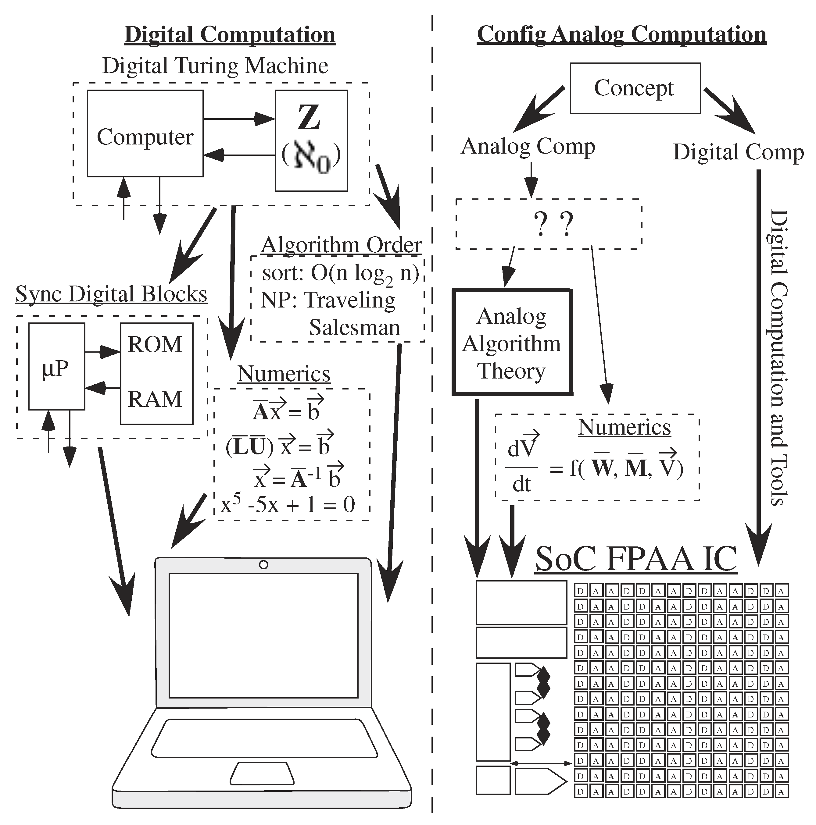
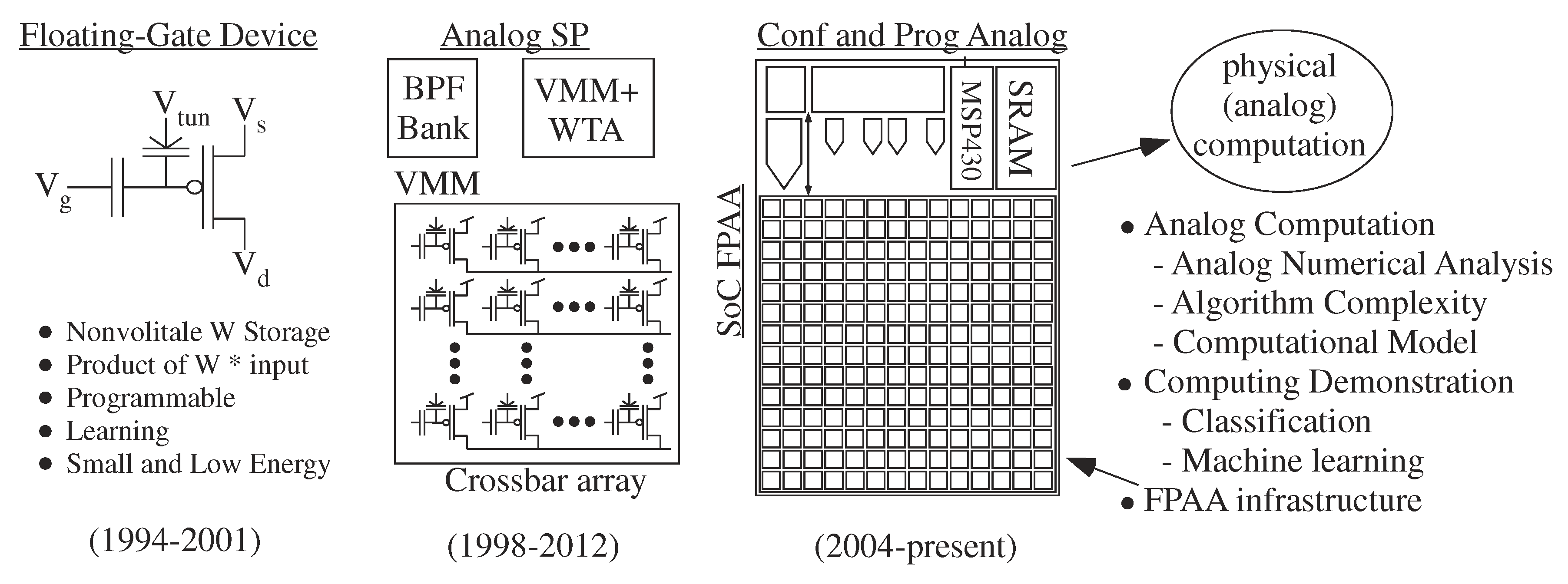
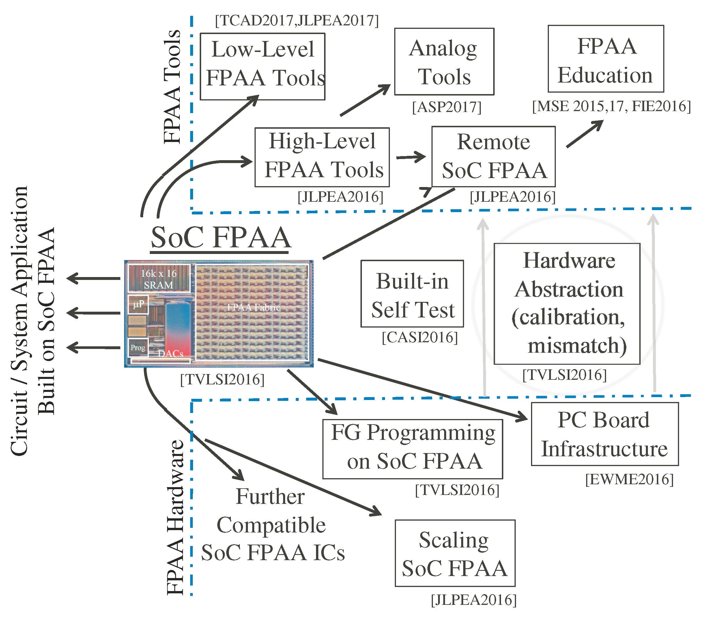
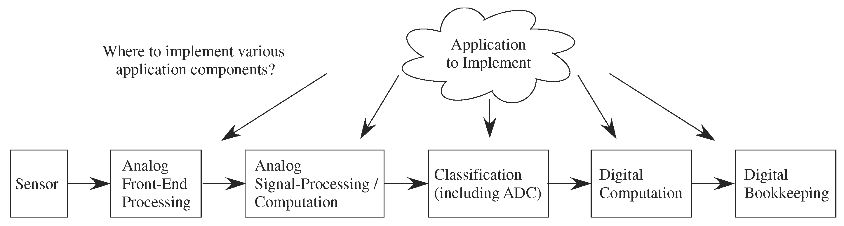
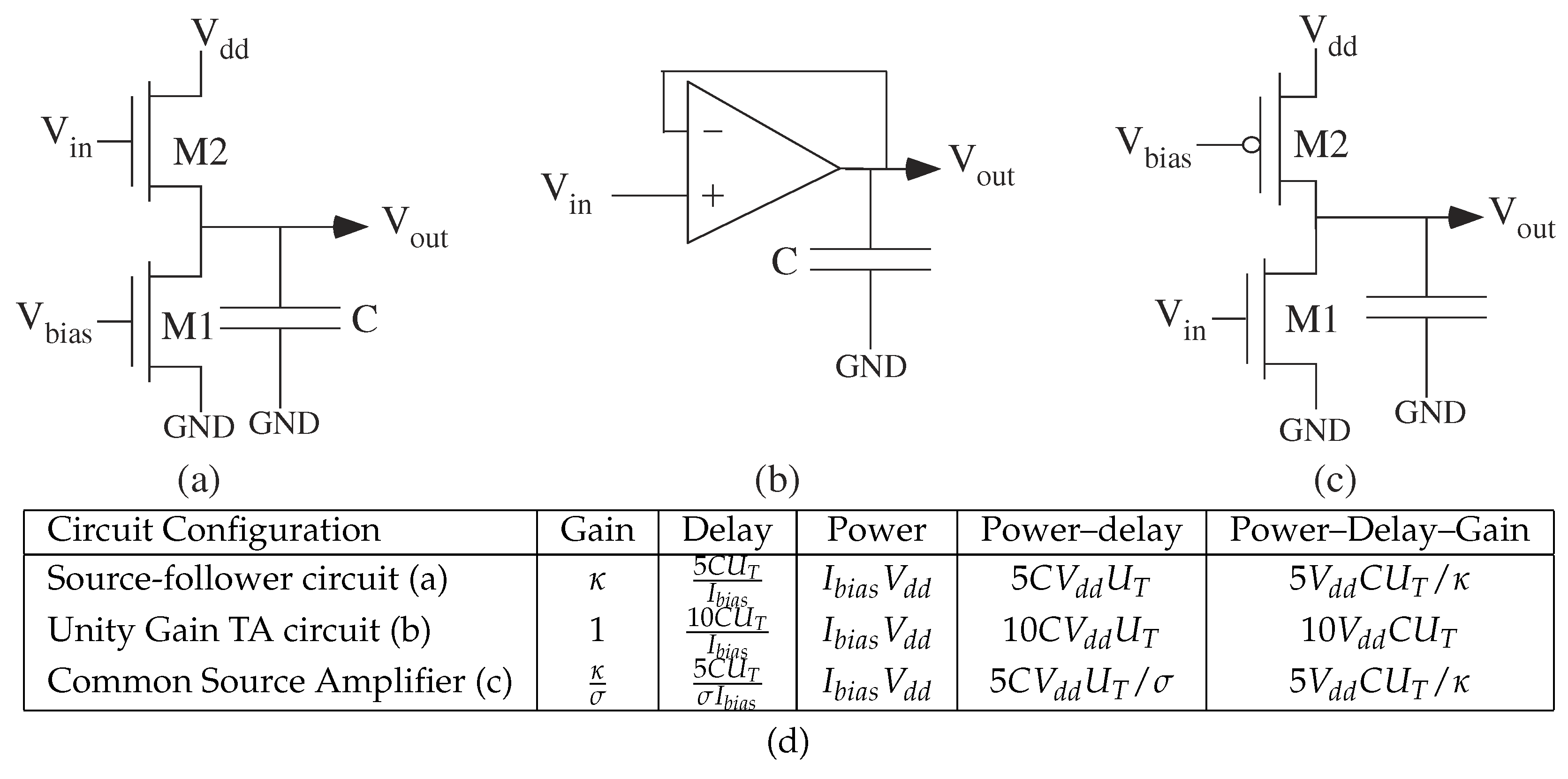
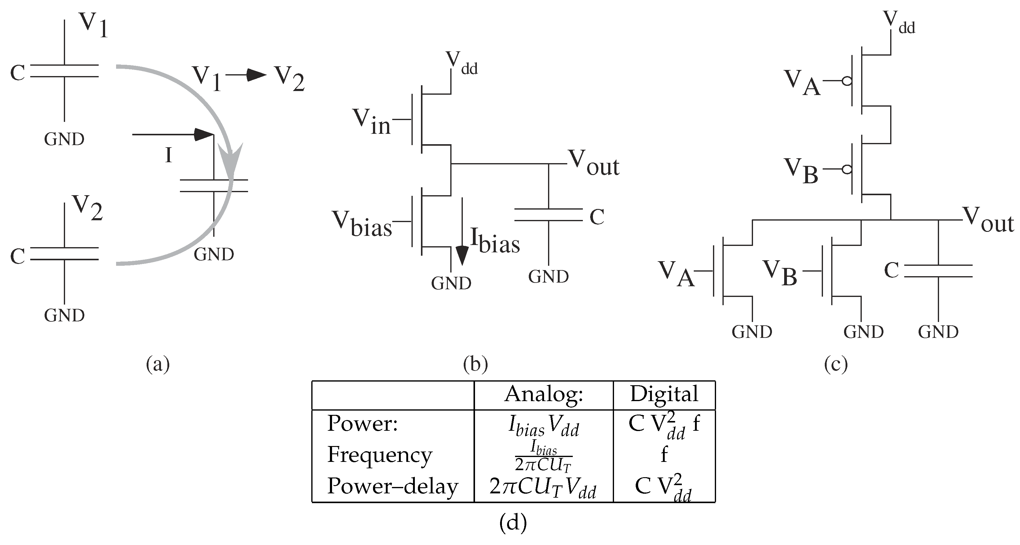
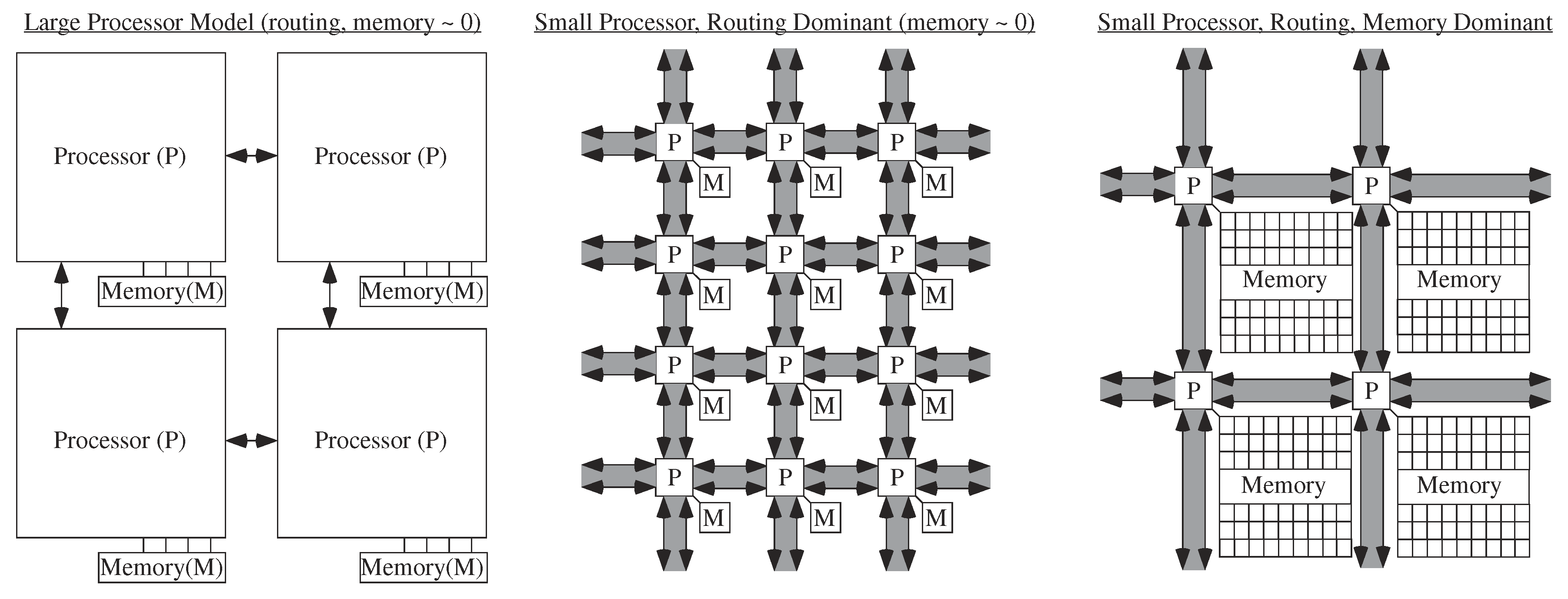
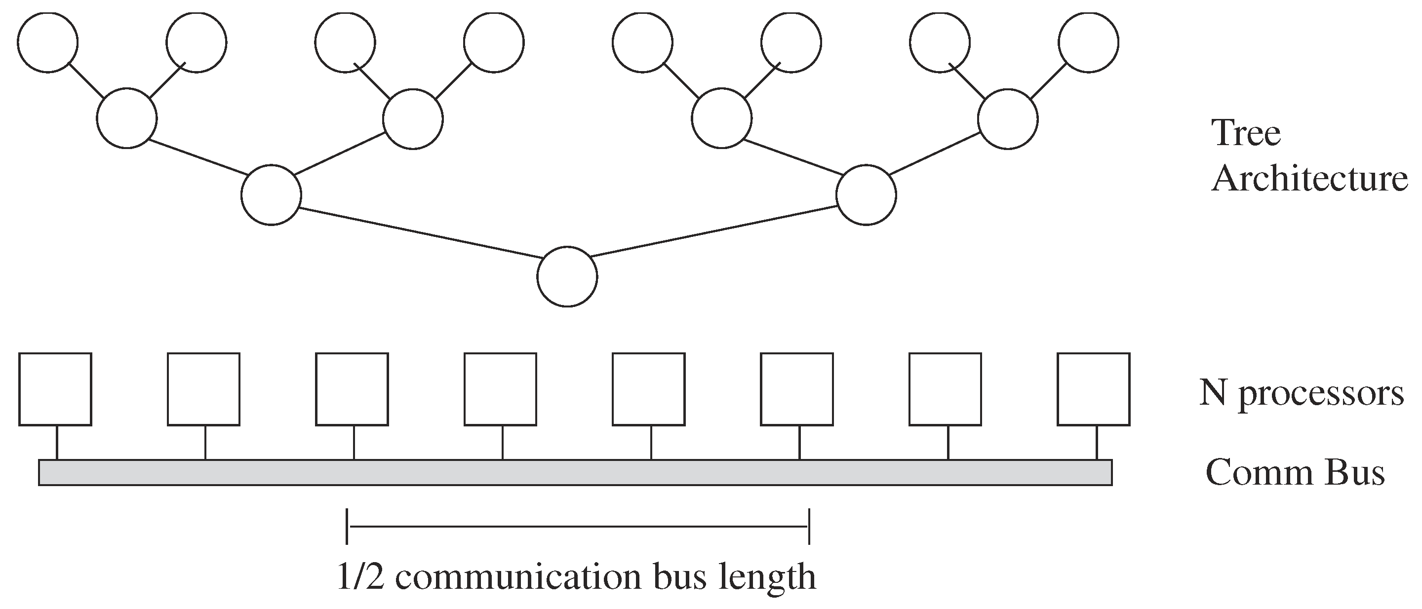
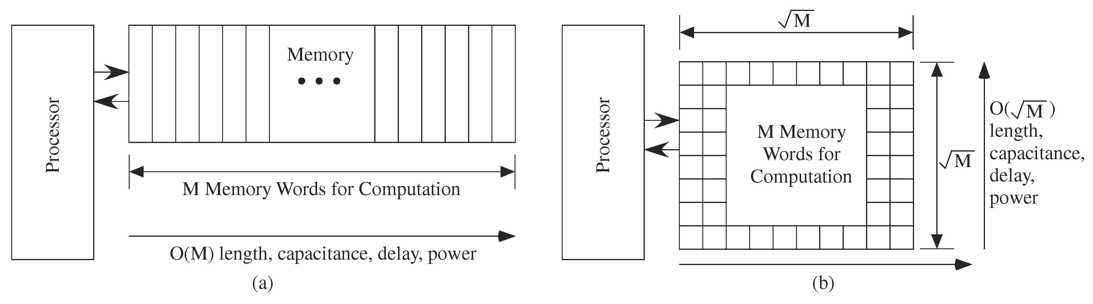
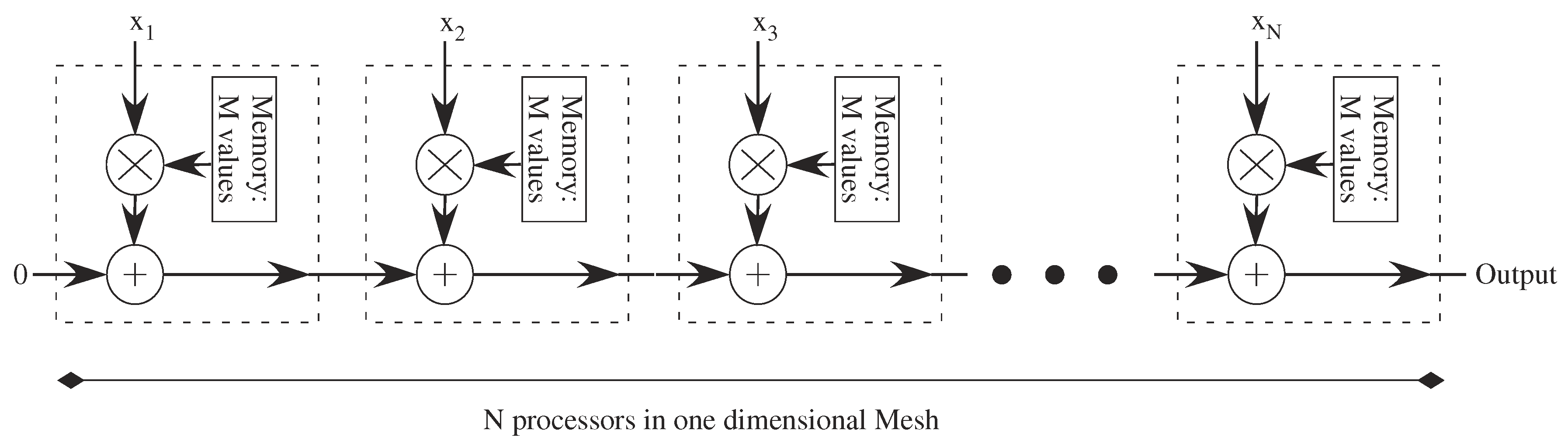
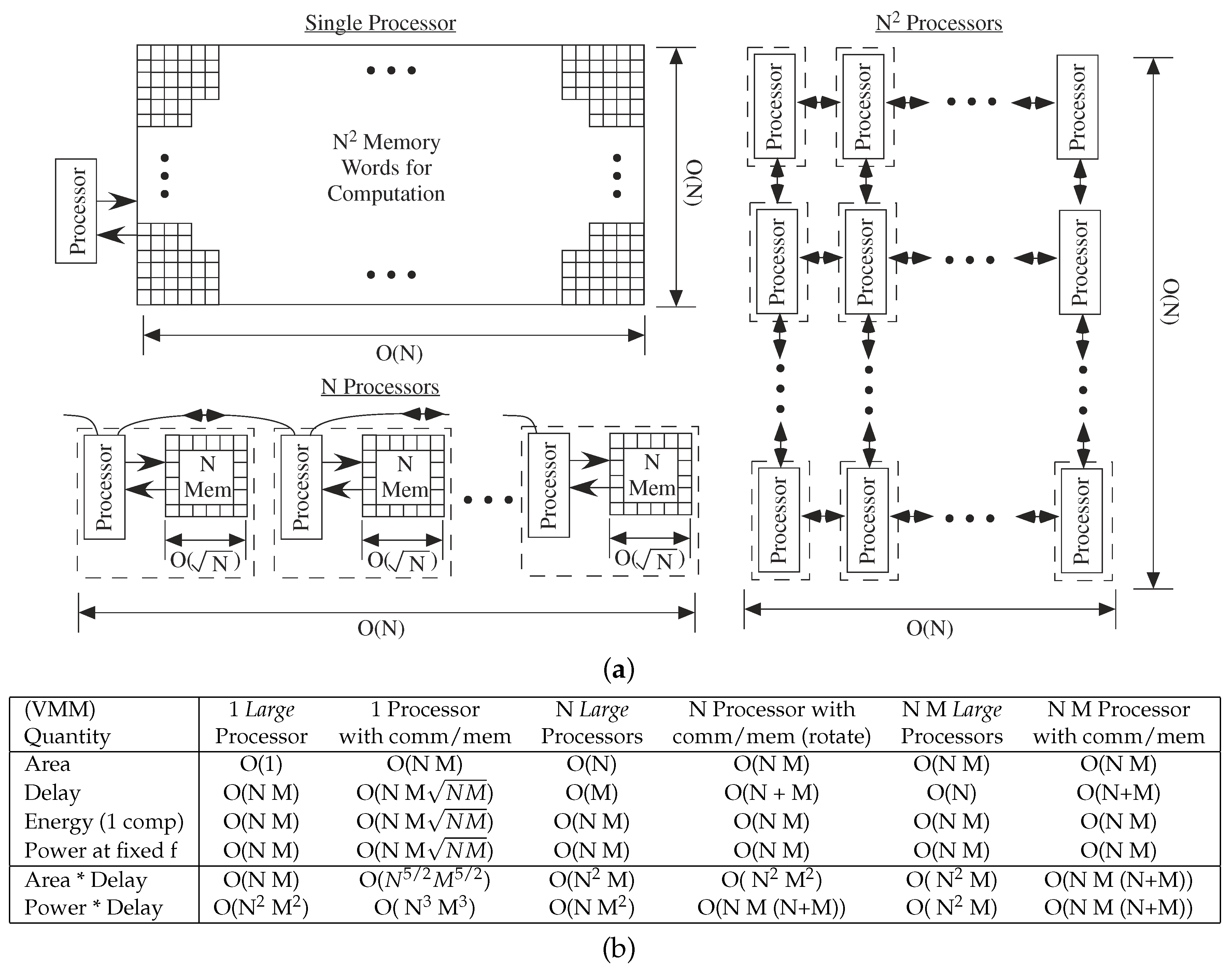
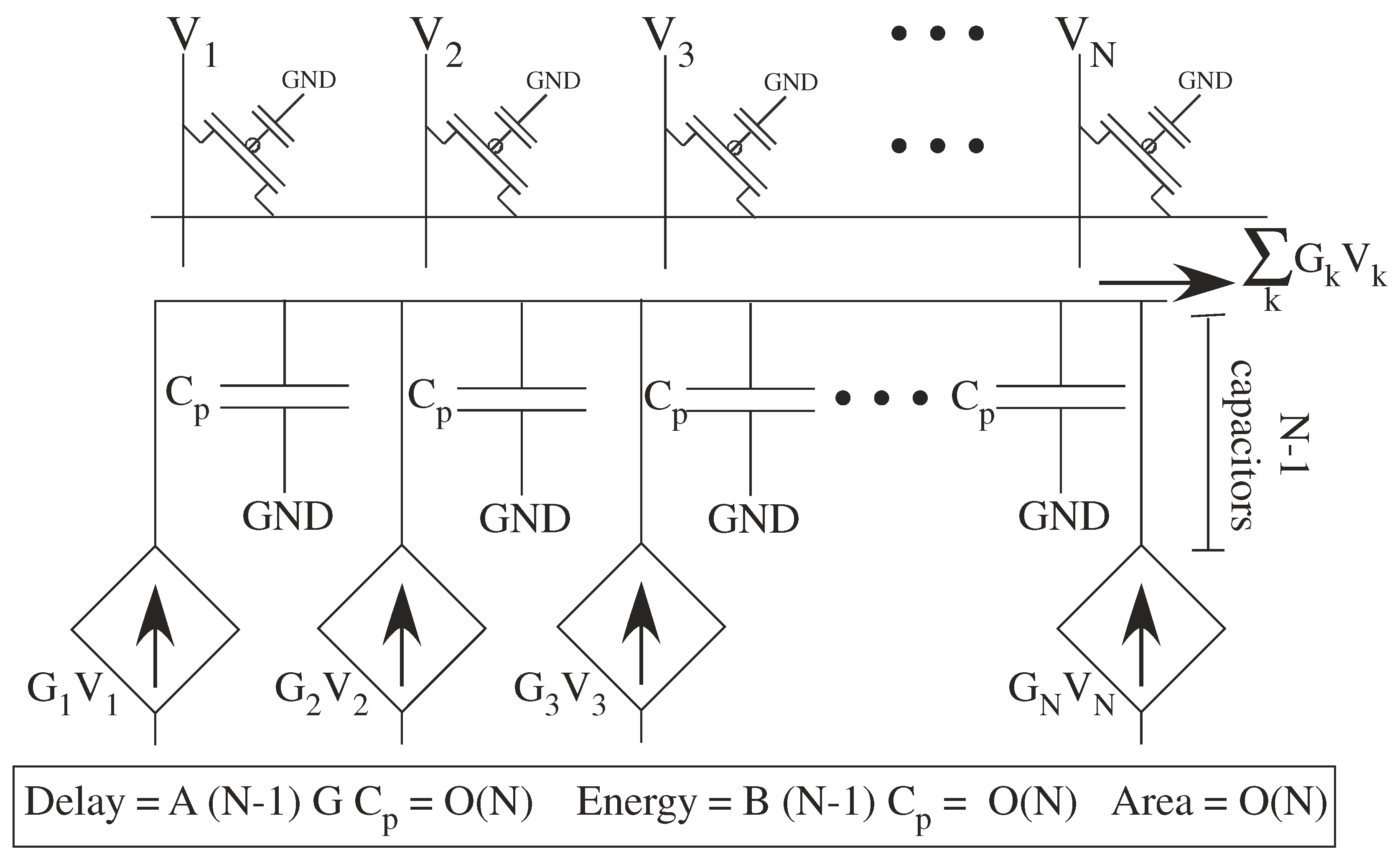
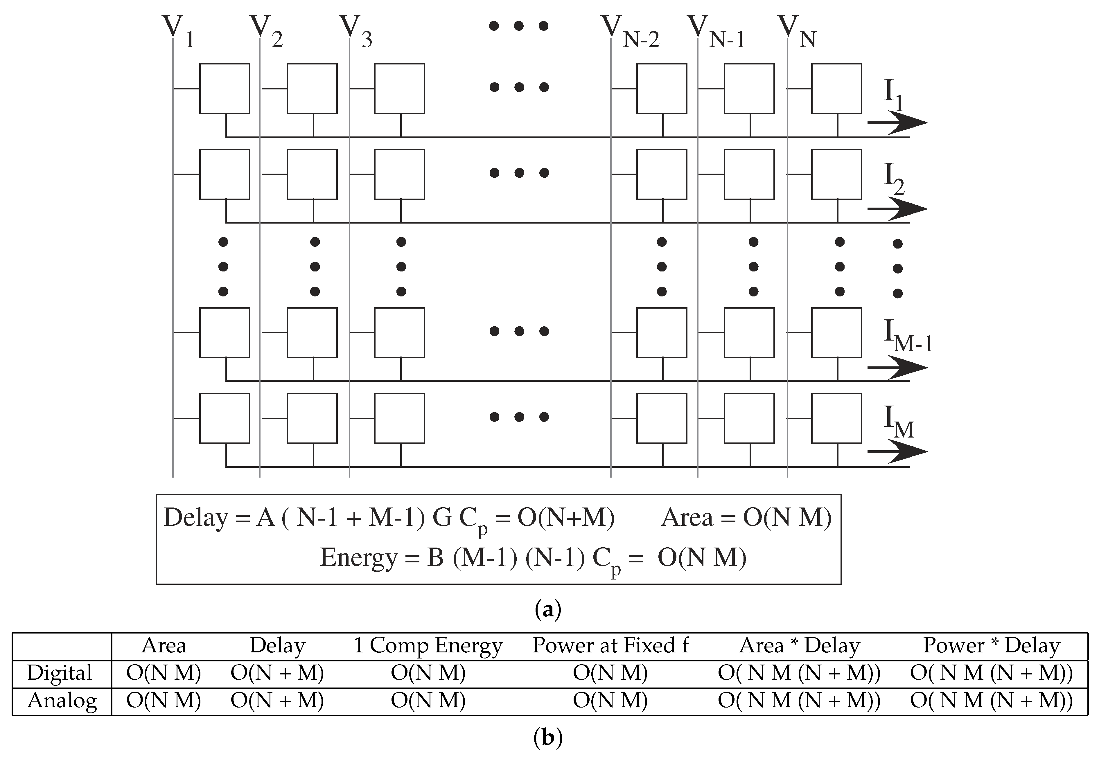
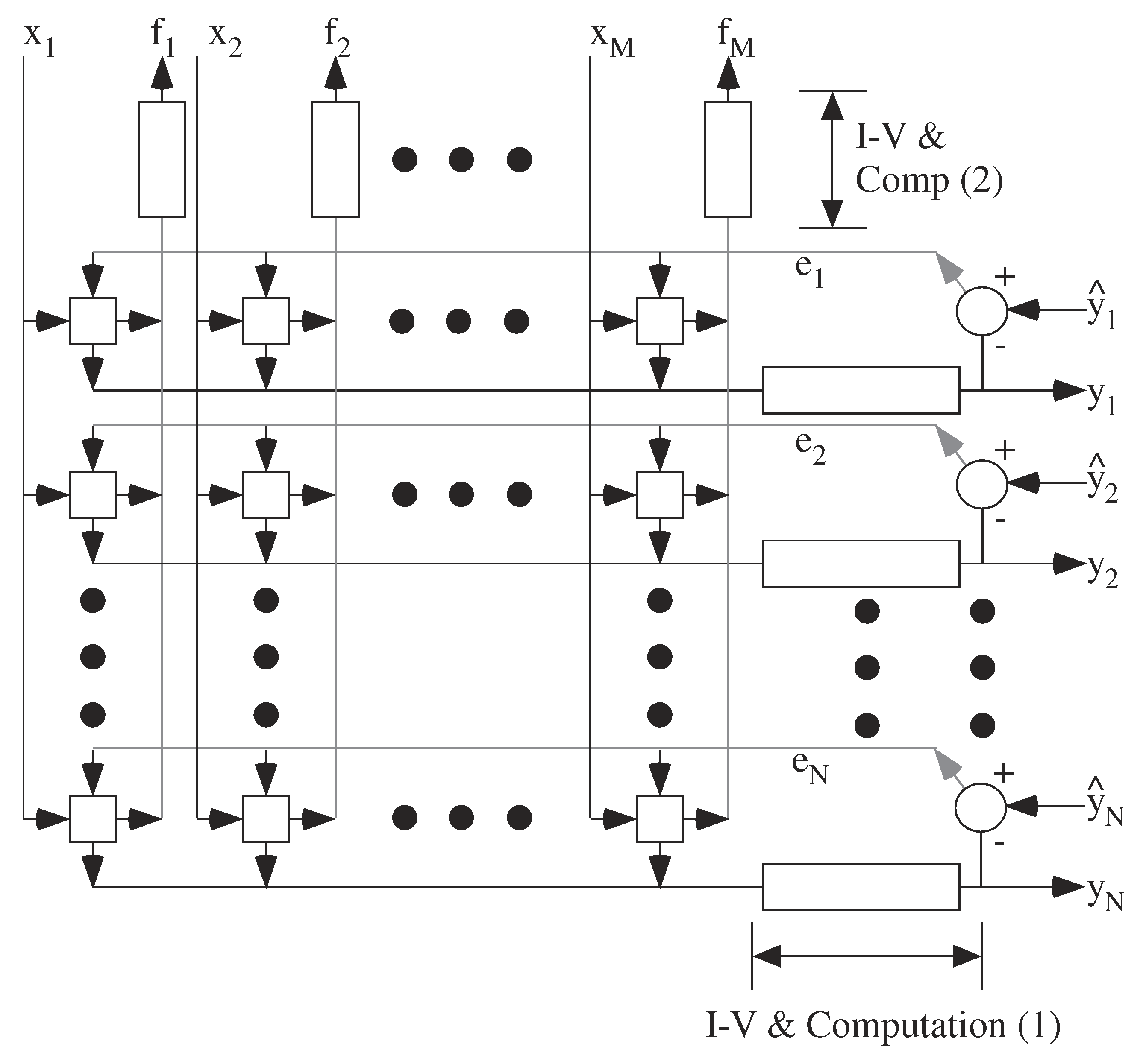
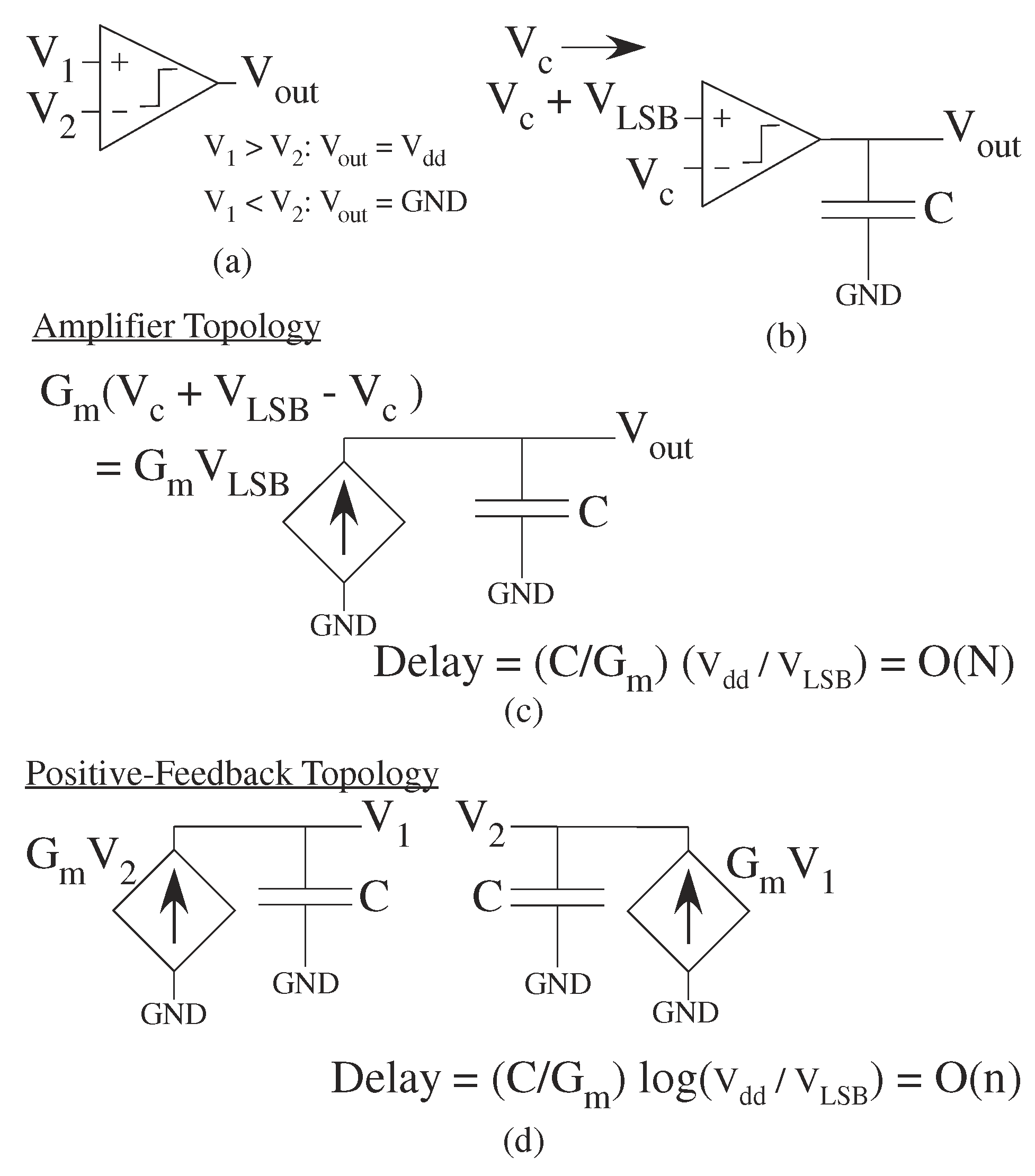
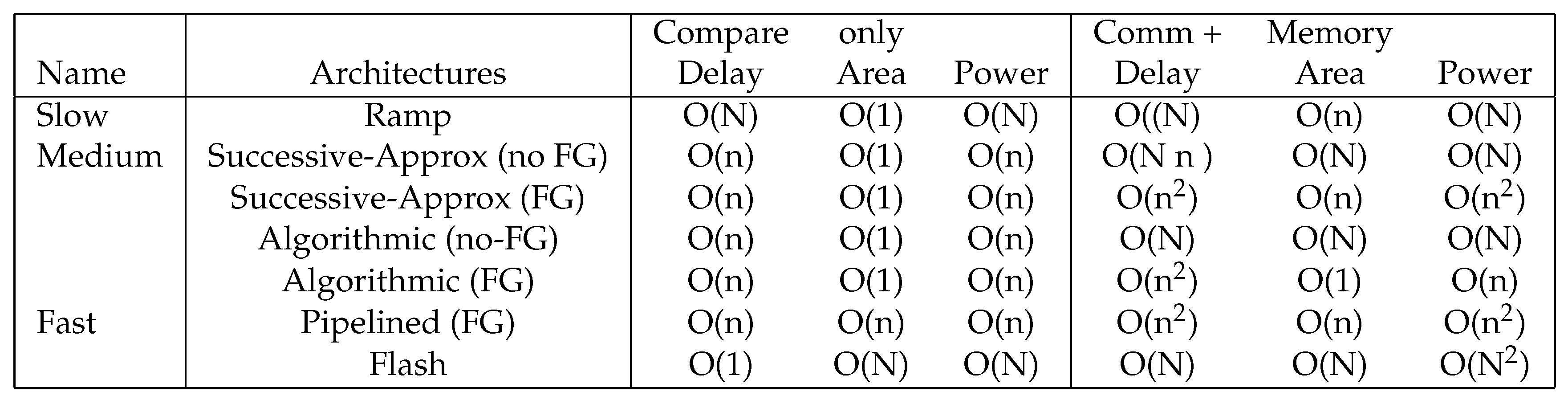
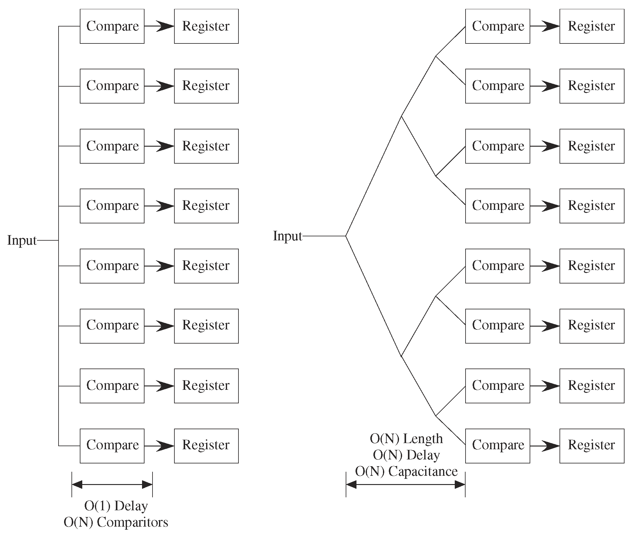
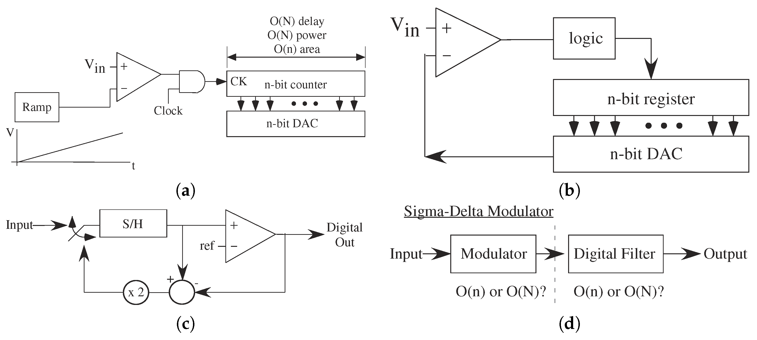
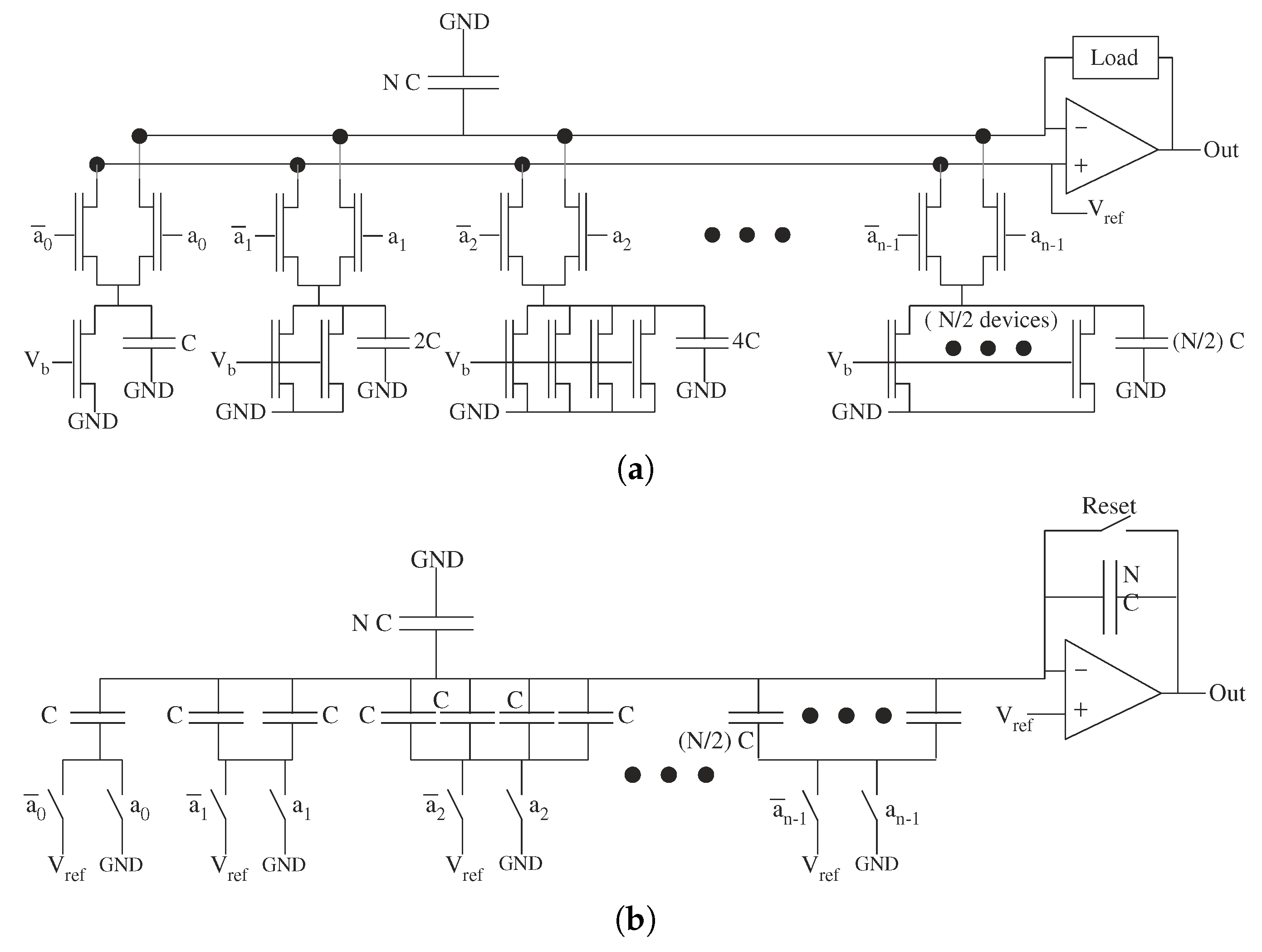
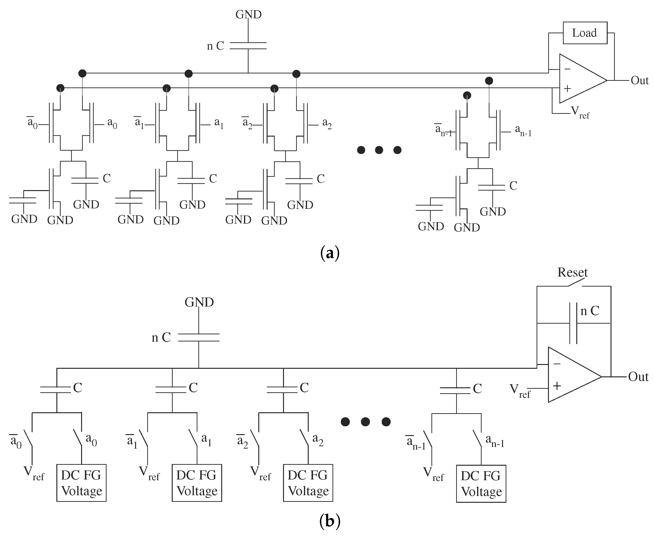
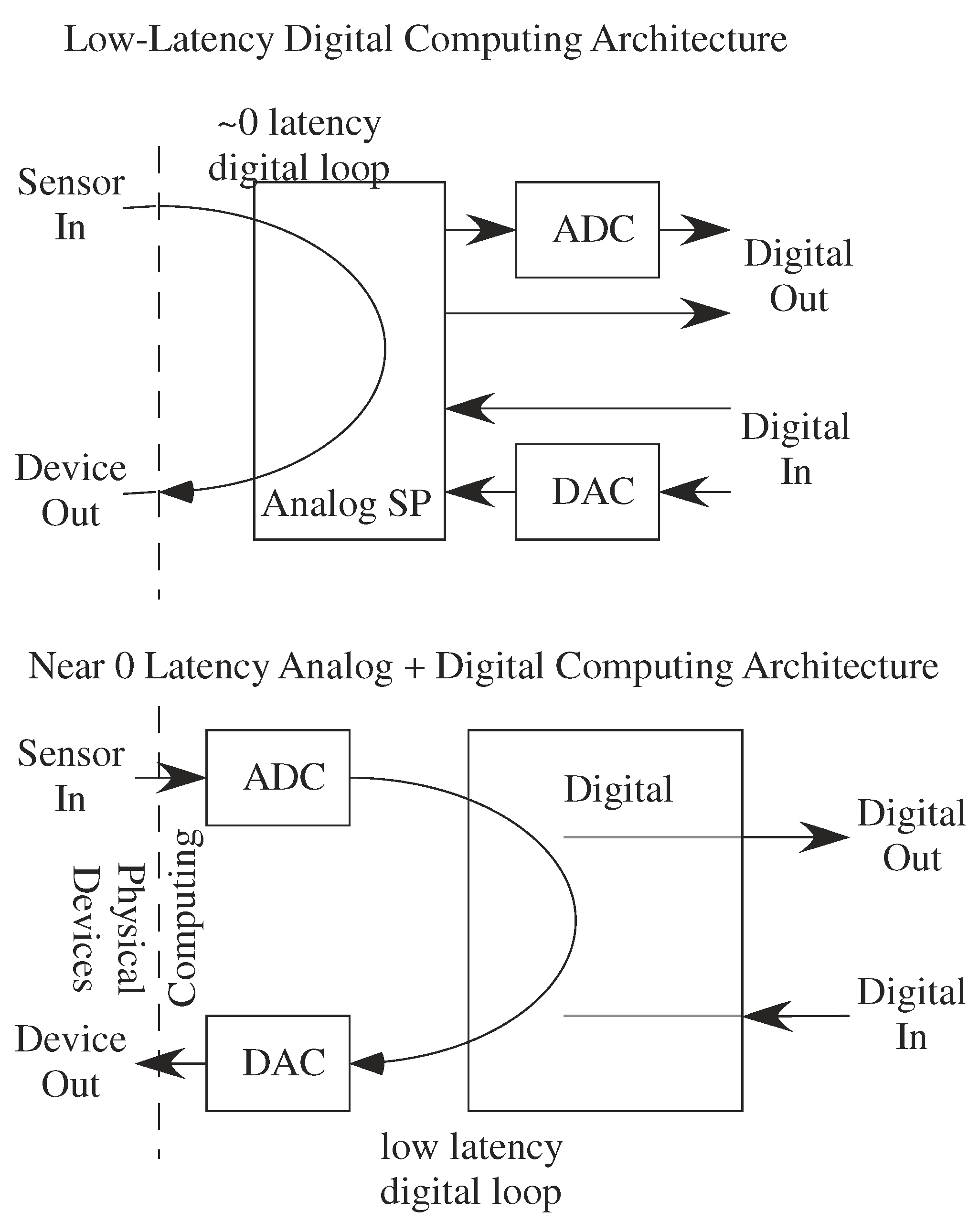
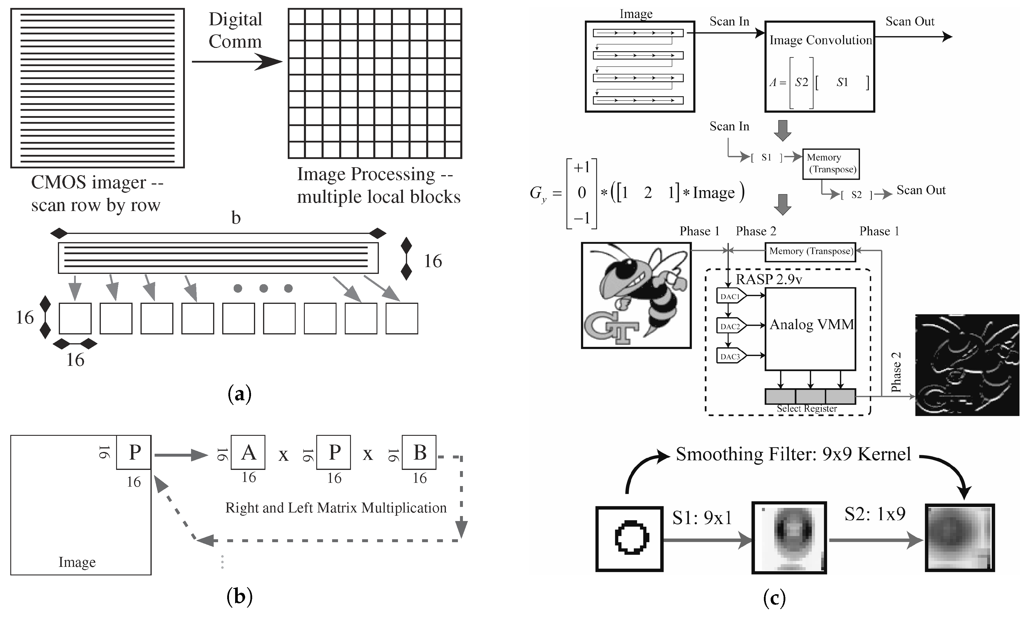
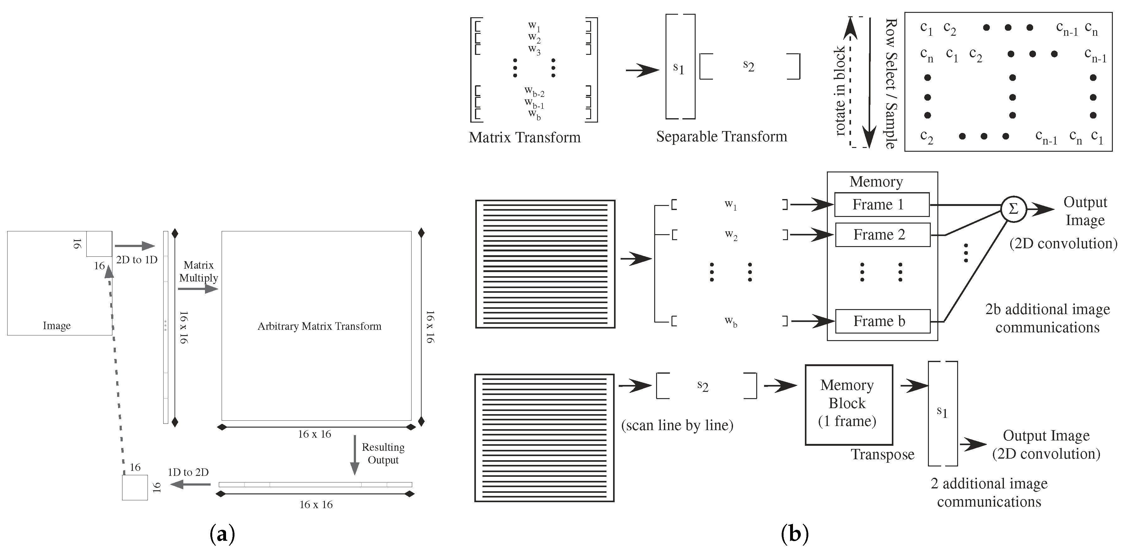
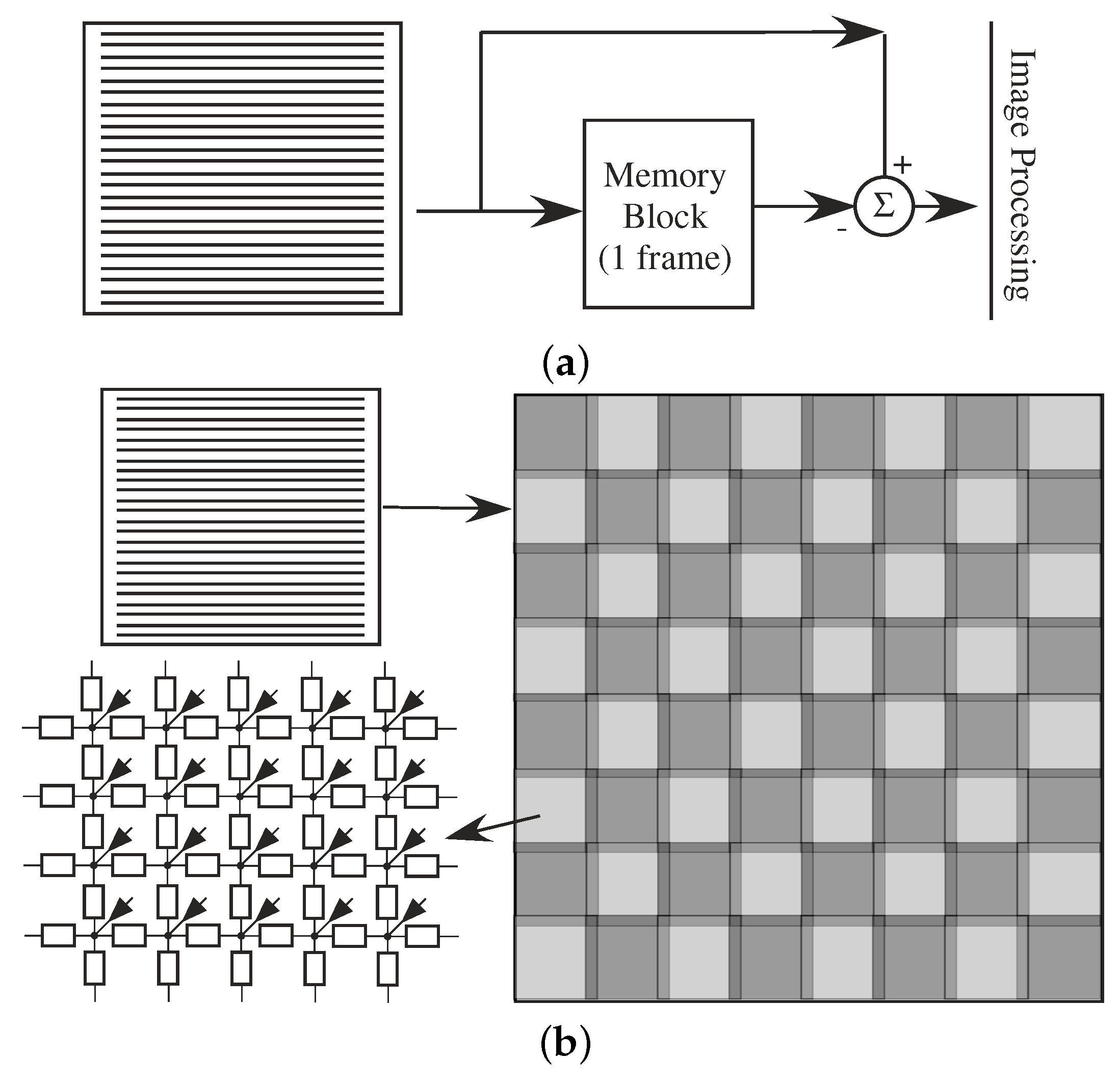
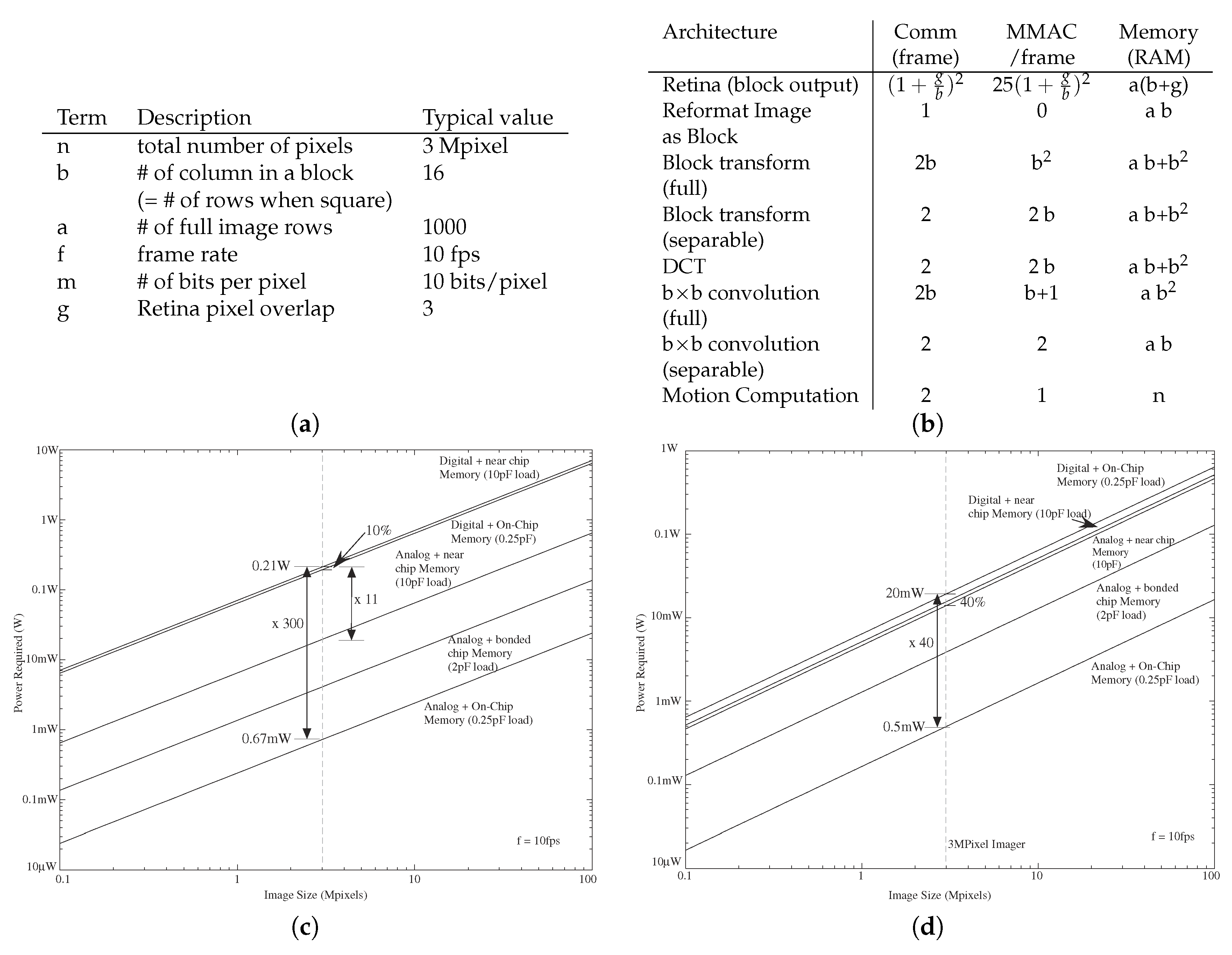
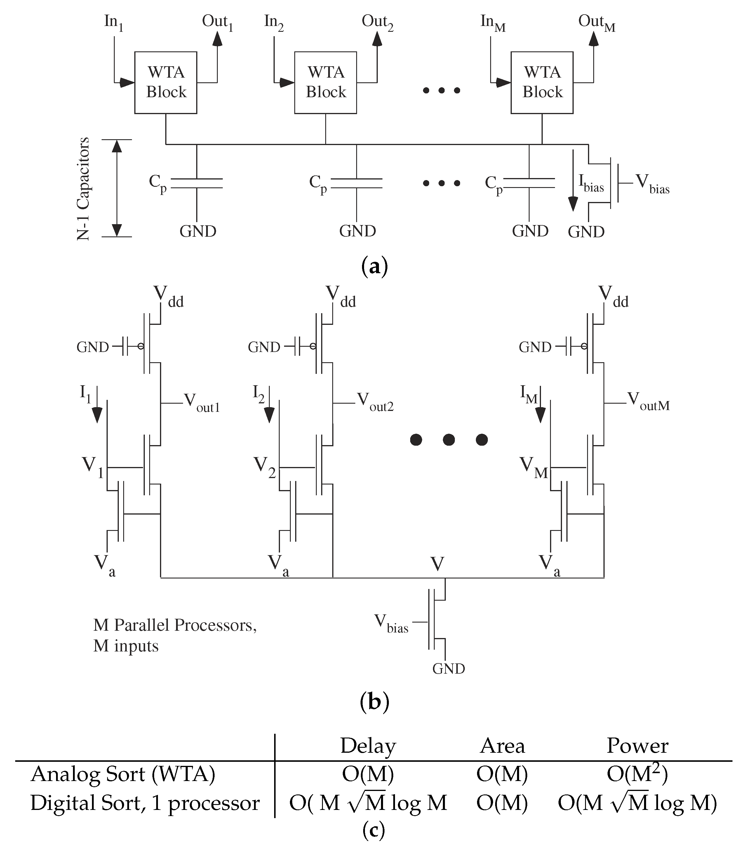
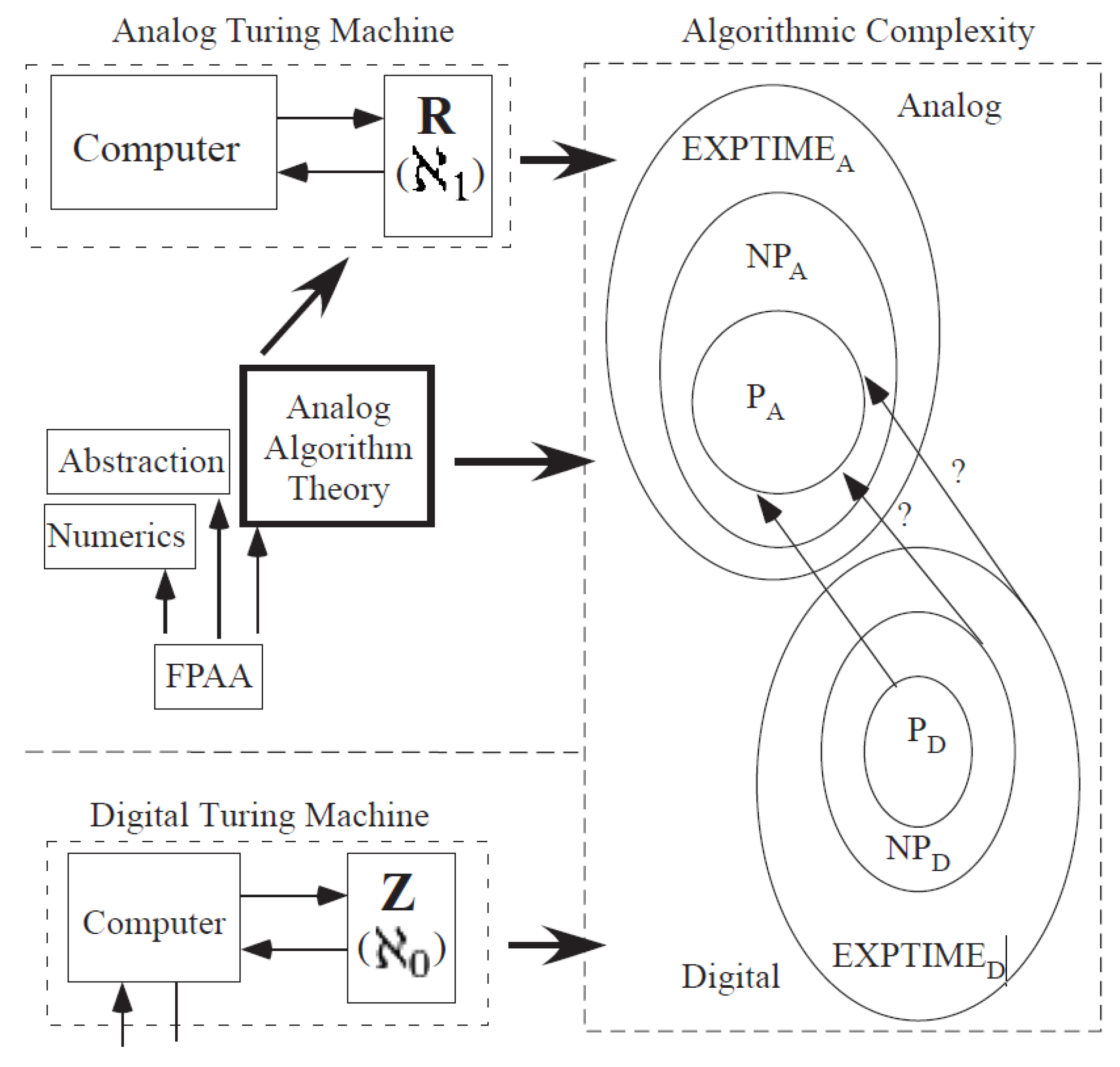
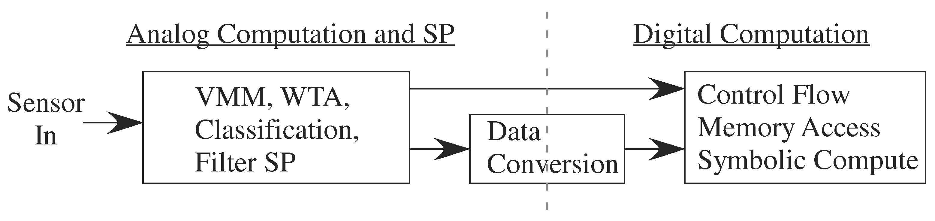
Table 1.
Metric summary for computing an FFT and/or DFT using 1, N, and N processors. An FFT computation provides no advantage compared to DFT for communication and memory access limited architectures.
Table 1.
Metric summary for computing an FFT and/or DFT using 1, N, and N processors. An FFT computation provides no advantage compared to DFT for communication and memory access limited architectures.
| Quantity | 1 Large Processor | B with comm/mem | 1 Processor + comm/mem | N Processors + comm/mem | N Proc. +c/m | N Proc +c/m |
|---|---|---|---|---|---|---|
| FFT | FFT | DFT | FFT | DFT | DFT | |
| Area | 1 | O(N) | O(N) | O(N) | O(N) | O(N) |
| Delay | O(N log N) | O(N log N) | O(N) | O( log N) | O(N) | O(N) |
| Energy (1 comp) | O(N log N) | O(N log N) | O(N) | O(N log N) | O(N) | O(N) |
| Area × Delay | O(N log N) | O(N log N) | O(N) | O(N log N) | O(N) | O(N) |
| Power × Delay | O(N log N) | O(N log N) | O(N) | O(N log N) | O(N) | O(N) |
© 2019 by the author. Licensee MDPI, Basel, Switzerland. This article is an open access article distributed under the terms and conditions of the Creative Commons Attribution (CC BY) license (http://creativecommons.org/licenses/by/4.0/).
Share and Cite
MDPI and ACS Style
Hasler, J. Analog Architecture Complexity Theory Empowering Ultra-Low Power Configurable Analog and Mixed Mode SoC Systems. J. Low Power Electron. Appl. 2019, 9, 4. https://0-doi-org.brum.beds.ac.uk/10.3390/jlpea9010004
AMA Style
Hasler J. Analog Architecture Complexity Theory Empowering Ultra-Low Power Configurable Analog and Mixed Mode SoC Systems. Journal of Low Power Electronics and Applications. 2019; 9(1):4. https://0-doi-org.brum.beds.ac.uk/10.3390/jlpea9010004
Chicago/Turabian StyleHasler, Jennifer. 2019. "Analog Architecture Complexity Theory Empowering Ultra-Low Power Configurable Analog and Mixed Mode SoC Systems" Journal of Low Power Electronics and Applications 9, no. 1: 4. https://0-doi-org.brum.beds.ac.uk/10.3390/jlpea9010004
Note that from the first issue of 2016, this journal uses article numbers instead of page numbers. See further details here.