A Fresh View on the Microarchitectural Design of FPGA-Based RISC CPUs in the IoT Era


Dipartimento di Elettronica, Informazione e Bioingegneria, Politecnico di Milano, 20133 Milano MI, Italy
*
Author to whom correspondence should be addressed.
J. Low Power Electron. Appl. 2019, 9(1), 9; https://0-doi-org.brum.beds.ac.uk/10.3390/jlpea9010009
Submission received: 14 January 2019
/
Revised: 6 February 2019
/
Accepted: 6 February 2019
/
Published: 19 February 2019
(This article belongs to the Special Issue Ultra-low Power Embedded Systems)
Abstract
:The Internet-of-Things (IoT) revolution has shaped a new application domain where low-power RISC architectures constitute the standard computational backbone. The current de-facto design practice for such architectures is to extend the ISA and the corresponding microarchitecture with custom instructions to efficiently manage the complex tasks imposed by IoT applications, i.e., augmented reality, artificial intelligence and autonomous driving, within narrow energy and area budgets. However, the new IoT application domain also offers a unique opportunity to revisit and optimize the RISC microarchitectural design flow from a more communication- and memory-centric viewpoint. This manuscript critically explores and optimizes the design of a RISC CPU front-end for IoT delivering a two-fold objective: (i) provide an optimized CPU microarchitecture; and (ii) present a set of three design guidelines to steer the implementation of IoT CPUs. The exploration sits on a newly proposed Systems-on-Chip (SoC) and RISC CPU implementing the RISC-V/IMF ISA and accounting for area, timing, and performance design metrics. Such SoC offers a reference design to evaluate pros and cons of different microarchitectural solutions. A wide combination of microarchitectures considering different branch prediction schemes, cache design architectures and on-chip bus solutions have been evaluated. The entire exploration is focused on the FPGA-based implementation due to the renewed interest for this technology demonstrated by both the research community and companies. We note that ARM launched the DesignStart FPGA program to make available the Cortex-M microcontrollers on Xilinx FPGAs in the form of IP blocks.
1. Introduction
The Internet-of-Things (IoT) revolution delivers a tightly interconnected world made of smart objects that are constantly collecting, processing, and distributing different data streams.
The embedded systems represent the computational backbone of such smart objects and are constantly evolving to meet the ever-increasing application and market requirements. Traditionally, 32-bit microcontroller-based platforms are used to ensure the required application performance while the ASIC-style implementation contributes to match low-power and small-area footprint requirements. However, the IoT scenarios are constantly evolving by continuously shaping novel and more demanding applications, i.e., high definition image processing, machine learning and artificial intelligence tasks, thus application-specific hardware accelerators have been coupled to microcontroller-based CPUs to offload the computation specific load. The use of such accelerators comes at the cost of a dramatically reduced platform flexibility thus making each device suitable for a narrow set of IoT applications. To fully restore the flexibility of the RISC computational platforms still meeting low area and energy requirements, the current de-facto practice is to extend the ISA with custom instruction sets to efficiently manage the complex tasks imposed by IoT applications, e.g., artificial intelligence, autonomous driving [1] and mesh processing [2] and computer graphics applications [3], within the RISC CPU still meeting low area and energy requirements. In this scenario, the IoT revolution contributed to the new golden age of RISC-based CPUs [4]. The RISC-V foundation [5] represents the most remarkable initiative to deliver a flexible ISA allowing several instruction extensions to accelerate the heavy tasks found in IoT applications. In particular, dozens of projects focused on the implementation of RISC-V-based CPUs and the related Systems-on-Chip (SoCs) to address different IoT applications by means of ad-hoc ISA extensions.
Such research domain is focused on the design and implementation of distinct microarchitectures to cope with the different computing challenges highlighted by the IoT. Each newly proposed microarchitecture sits on consolidated design practices and offers improved performance as well as low-power and area property by mostly leveraging the ISA extension opportunity. Such design practices have been taken from the high-performance computing (HPC) domain, where GPU- and High-Level-Synthesis-based (HLS) computing units are used to overcome the performance wall. We note that the IoT offers totally different challenges from the high-performance computing (HPC) for which energy-performance strategies for caches [6], on-chip interconnect [7,8] and computational units have been extensively explored. In particular, the HPC domain focuses on energy optimization under quality of service constraints, while the IoT domain aims to performance maximization subject to a given energy budget. To this extent, we strongly believe that the IoT revolution also offers the unique opportunity to critically revise the traditional microarchitectural design flow for RISC CPUs. Such new microarchitectural design approach can deliver an optimized general-purpose RISC CPU that can be enhanced in terms of custom ISA instruction extensions within a second design step.
The manuscript starts by revising the standard microarchitectural building blocks of the RISC CPUs and SoCs in the IoT domain focusing on the communication- and a memory-centric design approach with two final goals. First, we explore the intricate relationship between the on-chip interconnect, the cache hierarchy and the CPU microarchitecture considering three orthogonal design metric, (i) performance, (ii) timing and (iii) area. Second, we deliver a set of three guidelines to optimally design the CPU microarchitecture in the IoT domain. In particular, the focus is on the microarchitecture of the CPU front-end as it can severely impact the overall CPU design metrics. Both the analysis and the proposed microarchitectural optimizations employ a newly proposed SoC and RISC CPU, matching the RISC-V/IMF ISA specification. The proposed SoC and CPU have been designed and implemented focusing on the FPGA design flow. Such focus is due to the recent technological improvements of FPGA technology and the great interest demonstrated by both the research community and the companies. We note that several RISC-V projects for IoT target FPGA chips. Moreover, ARM Ltd has recently launched the DesignStart FPGA program to make available the Cortex-M series microcontrollers for Xilinx FPGA users in the form of IP blocks [9] with the clear intent to support FPGA-based IoT platforms.
Contributions—This research is focused on the standard microarchitectural components only, without considering any ISA extension since they have been widely explored in the available open literature [10,11] and contributes to the state of the art in two different directions:
- Communication and memory-centric design evaluation. We explored the intricate relationship between the cache, the on-chip interconnect and the branch prediction schemes to optimally design the SoC microarchitecture of IoT platforms. The analysis considers timing, area and performance design metrics to offer a complete set of pros and cons for different microarchitectural solutions still ensuring their implementation feasibility.
- Set of design guidelines for IoT RISC CPU on FPGA. Such guidelines are drawn from the results obtained after the complete evaluation of all the proposed microarchitectural variations on a newly designed RISC CPU implementing the RISC-V ISA. The newly proposed RISC CPU represents a common substrate that enables the focused evaluation of pros and cons for each microarchitectural variation.
The rest of the manuscript is organized in five parts. Section 2 reviews the state of the art on publicly available load-store RISC CPUs also highlighting the differences between this work and the contributions in the open literature. The microarchitecture of the proposed CPU and SoC implementation used as reference platform as well as the proposed microarchitectural optimizations are discussed in Section 3. Section 4 reports the results in terms of timing, area, and performance for each considered microarchitecture. A set of guidelines to design IoT RISC CPU on FPGAs is provided in Section 5. Conclusions and future works are drawn in Section 6.
2. Related Works and Background
The IoT greatly fueled the research effort in RISC architectures with a dramatic increase in the number of open-hardware solutions delivering a full set of non-obfuscated CPUs targeting the low- and middle-end IoT domains (see Table 1). We note that each proposal in the open literature is focused on performance optimization considering a specific ISA extension also employing standard microarchitectural design patterns for both CPU and SoC without evaluating possible optimizations of the latter. In contrast, this manuscript focuses on the optimization of the standard microarchitectural design patterns for CPU and SoC employed in the IoT and low-end embedded domains.
The OpenRISC Platform SoC (ORPSoC) Version 3 [13] is the first complete example of open-hardware processor implementing the royalty-free OpenRISC 1000 architectural specification [20]. The AR100 power management unit in Allwinner SoCs [21] employed an OpenRISC 1000 processing unit and the OpenRISC 1000 architecture is supported in the mainline Linux Kernel since version 3.1 [22].
Several OpenRISC 1000 compliant CPUs have been developed in recent years implementing standard caches, on-chip bus as well as branch prediction schemes [12].
The RISC-V ISA is a recent ISA specification that represents the de-facto standard for open-hardware computing platforms for IoT and embedded domains.
The PULP project [11] offers single- and multi-core accelerators for embedded platforms implementing the RISC-V ISA [5] where PULPino is the ultra-low-power platform for IoT applications. The PULP project primarily targets ASIC implementations to deliver low-power solutions. However, the technology improvements of FPGA solutions fueled the introduction of the HERO platform, an FPGA-based architecture made of PULP-based soft-cores [23].
The Berkeley Rocket chip generator [14] is written in Chisel domain specific language and can generate different instances of the Rocket RISC-V processing unit. The Rocket processing unit is the computing CPU of the Celerity [24] and the VELOUR [25] SoCs. The Celebrity SoC employs a parallel accelerator fabric coupled with a neural network accelerator implemented using Rocket CPUs. The VELOUR SoC features a Rocket-based CPU coupled with a deep neural network accelerator. In addition, the Berkeley BOOM-v1 [16] and Berkeley BOOM-v2 [17] are two super-scalar, out-of-order RISC-V processors targeting high-end embedded applications.
The open literature also reports several RISC-V-based SoC targeting FPGA implementations. The VexRiscv project [18] offers a set of simple, FPGA-compliant high-clock-frequency RISC-V CPUs. Some of the proposed CPUs offer interactive debug support and extensive performance, area and clock frequency statistics. However, the implemented CPUs do not consider any optimized microarchitecture for caches, on-chip bus, and branch predictions schemes.
The Orca CPU [15] is a simple RISC-V scalar core targeting FPGA implementation. The mriscv SoC implements a complete RISC-V-based microcontroller [26] offering ADCs, DACs, GPIO, and SPI interfaces.
The GRVI Phalanx FPGA-based accelerator framework [19] is a shared-memory platform made of simple RISC-V scalar cores coupled with specialized accelerators. Similarly, Taiga is a RISC-V 32-bit soft processor that can be used in configurable FPGA-based multi-core frameworks used for heterogeneous computing [27].
Despite the wide variety of FPGA- and ASIC-based open-hardware IoT platforms, all the proposals are focused on delivering new CPU implementations for different application domains. In particular, each solution reports the performance comparison between different CPU implementations without considering pros and cons, i.e., performance, timing and area increase/decrease, that different microarchitectural optimizations can have on the same baseline microarchitecture. For example, the PULP-based Ariane solution employs a FIFO queue in place of a standard instruction cache as the one employed some of the OpenRISC CPU implementations. However, no comparison in terms of performance or feasibility between the two cache solutions has been proposed so far. Moreover, the intricate relationship between the on-chip interconnect and the cache hierarchy has not been evaluated yet. To the best of our knowledge, this work is the first research that analyzes and optimizes the design of FPGA-based load-store RISC CPU considering the combined pros and cons of four microarchitectural components: (i) instruction cache, (ii) on-chip interconnect, (iii) branch prediction schemes and (iv) instruction bus width.
3. Architectural View of the Proposed IoT Processor
This section overviews the developed RISC-V, in-order CPU and the related SoC that are used in the rest of the manuscript as representative use-case to explore the microarchitectural design space. The goal is to deliver a reference CPU and SoC implementation to carefully evaluate pros and cons of different microarchitectural solutions for the CPU front-end design in terms of performance, area and timing (see Section 3.1). In general, the architectural and microarchitectural exploration of general-purpose multi-cores sits on cycle accurate simulators [28] eventually equipped with power and area models for a part or the entire simulated platform [29,30]. In contrast, IoT scenarios leverage simpler architectures for which the gate-level exploration is feasible and is far more informative thanks to the accurate timing and area estimates of a fully implemented design.
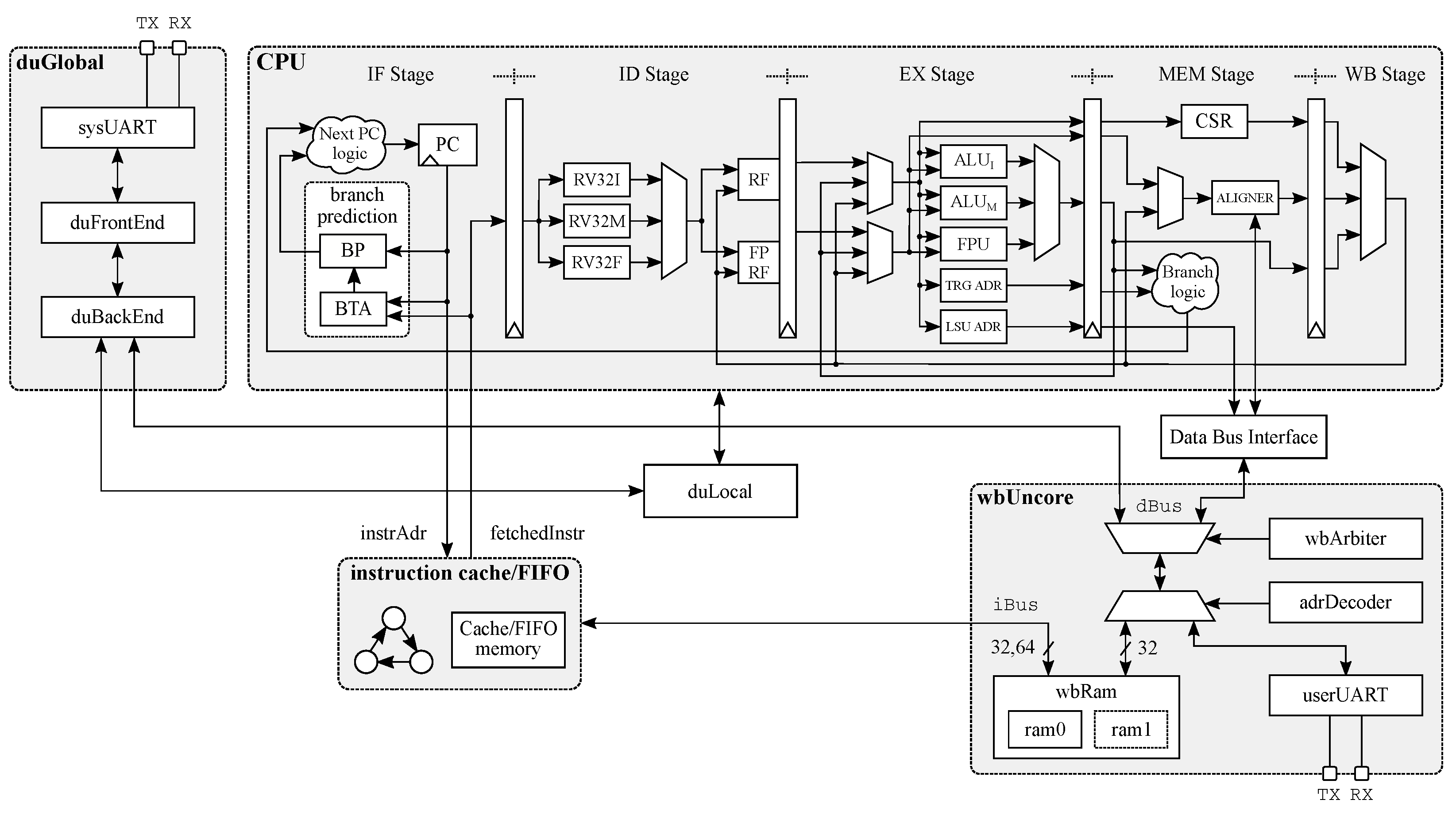
The reference SoC is made of a 32-bit RISC-V compliant CPU, a 64KiB main memory implemented employing Xilinx BRAMs and a Wishbone [31] compliant bus connecting the two, implementing both burst as well as single read/write transactions. The debug unit (duGlobal) represents a second on-chip data bus master that is used to interface the entire platform with the host laptop, via the system UART (sysUart), for in-circuit debugging and on-prototype simulations. Last, a user UART is implemented to allow read and write operations at software level.
A schematic view of the proposed SoC is depicted in Figure 1. We implemented two separate bus interconnects for instructions and data to minimize the contention problem. Moreover, the instruction bus is a point-to-point connection when a single CPU is implemented, thus no bus arbitration is required. In contrast, a round-robin bus arbiter is used to arbitrate the data bus where both the CPU and the duGlobal can request the access as masters. In the baseline SoC, a Simple-Read/Write transaction on the instruction bus takes 2 clock cycles, i.e., the first to open the transaction and the second to read (write) data from (to) the synchronous memory. The same transaction requires three clock cycles on the data bus due to the bus arbitration stage that takes one extra clock cycle. We note that the baseline SoC also implements the burst transactions as defined in the Wishbone protocol specification [31] to optimize multiple data transfers.
The proposed CPU features a single-issue, in-order, 5-stage pipeline implementing the standard Integer (I), Multiply (M), Floating Point (F) extensions of the RISC-V ISA.
The Instruction Fetch (IF) stage of the CPU can fetch up to a single, 32-bit, fixed-length instruction per clock cycle. Moreover, the program counter is updated in the same clock cycle following the standard RISC-V ISA architectural specification manual [5].
In the baseline CPU, the IF stage takes two clock cycles to load each instruction leveraging a Simple-Read Wishbone transaction since no caches are implemented as well as the branch prediction schemes. The complete evaluation of the branch prediction schemes and cache microarchitecture is part of the contribution of this work and is carefully detailed in Section 3.1.
The Instruction Decode (ID) stage extracts from the fetched instruction the information required to drive the Register File (RF), the Floating Point Register File (FP-RF) and the immediate operand logic to set up the operands for the execution stage. A separate Instruction Decoder for each implemented RISC-V extension is provided to easily allow disabling different ISA extensions at synthesis time. The ID stage also forwards the signals derived from the instruction operation code (opcode) to the five Functional Units (FUs) implemented in the EX stage, i.e., the Arithmetic-Logic Unit (), the Integer Multiply and Divide (), the Load-Store Adder Unit (LSU-ADR), the Floating Point Unit (FPU) and the jump/branch ALU (TRG-ADR). In the EX stage, the operands are multiplexed with the results from the memory (M) and write-back (WB) stages to implement the EX-EX and M-EX forwarding paths [32]. Moreover, the M-M forwarding path is also implemented in the M stage to optimize the load-store instruction patterns [32]. We note that both the address and the condition of the branch instructions are computed in the EX stage while the PC update due to a control-flow instruction is delayed up to the M stage as in the standard RISC pipeline [32]. The implemented branch evaluation microarchitecture is sub-optimal compared to those that anticipate the PC update in the EX or even in the ID stages. However, we leverage such implementation to magnify the penalty of any branch misprediction thus the gap between different evaluated solutions.
Microarchitectural Optimization of the Instruction Fetch Stage
This section describes the three microarchitectural parts that are explored in the rest of this work: (i) branch prediction scheme, (ii) instruction cache/FIFO and (iii) the use of 32-/64-bit instruction bus width on 32-bit architectures.
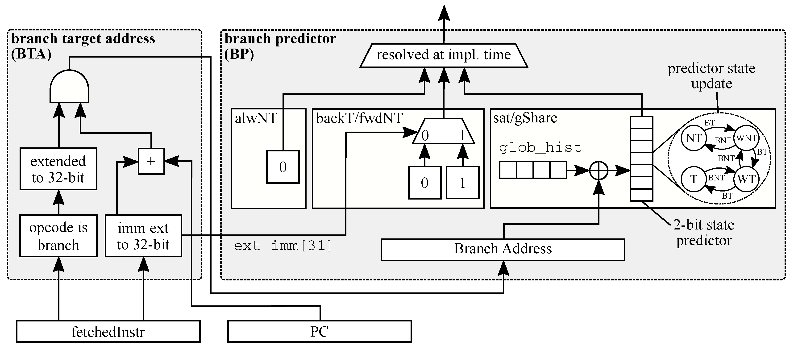
The branch prediction scheme represents a critical microarchitectural component to sustain the CPU performance. It minimizes the number of branch mispredictions and the corresponding misprediction penalty. It is important to note that we are not proposing novel branch prediction schemes. In contrast, the contribution sits on the critical evaluation of reference branching schemes from performance area and timing viewpoint. Such analysis allows to pinpoint the correct scheme to implement considering the performance requirements as well as the energy and timing constraints. Figure 2 shows the four standard branch prediction schemes considered in this work. We use the always not taken (alwNT) when the CPU is not implementing any branch prediction scheme. Moreover, we consider the standard static and dynamic branch prediction schemes, i.e., the backward taken forward not taken (backT/fwdNT)—static—as well as the saturation (sat) and the gShare—dynamic. The sat scheme is a gShare with a single 2-bit state finite state machine and no global-history vector. Moreover, the proposed gShare branch predictor features 32 entries and a 5-bit global-history vector since the experimental results show no performance improvement from a larger number of entries or a longer global-history vector.
The backT/fwdNT offers a simple implementation with low area footprint since the scheme has no internal state. In particular, the direction of the branch, is evaluated by checking the 31-st bit of the extended immediate value that is expressed as two’s complement number (see Figure 2). In contrast, both the sat and gShare implementations impose a bigger area footprint due to the 2-bit state saturation predictors as discussed in Section 4. We note that no branch target buffer is used thus if the address cannot be computed from the branch/jump instruction, e.g., jump register instruction type, the fetch stage loads the next instruction in program order. Such implementation choice is motivated by the need to contain both the area footprint and the timing slack. In particular, our evaluation considers the cache/FIFO lookup and the branch prediction in a single clock cycle to avoid splitting the IF stage in two stages, thus making the pipeline deeper. In this scenario, the cache architecture can constraint the selection of the branch prediction scheme.
The instruction bus width represents another considered design parameter in our evaluation. We considered a 32-bit architecture with the possibility to implement a 32- or 64-bit instruction bus. The 32-bit instruction bus represents the standard solution adopted in the majority of the implemented 32-bit architectures. In contrast, the 64-bit instruction bus offers a low latency solution since two 32-bit instructions can be fetched for each clock cycle. As the results reported in Section 4 confirm, the use of a 64-bit instruction bus does not severely affect timing or area and offers superior performance to both miniCache and FIFO queue designs.
The 64-bit bus allows a faster cache-line refill for the miniCache architecture with a net miss penalty reduction. In contrast, the FIFO scheme coupled with the prefetcher can reach full throughput for all the programs that execute instructions in strict program order.
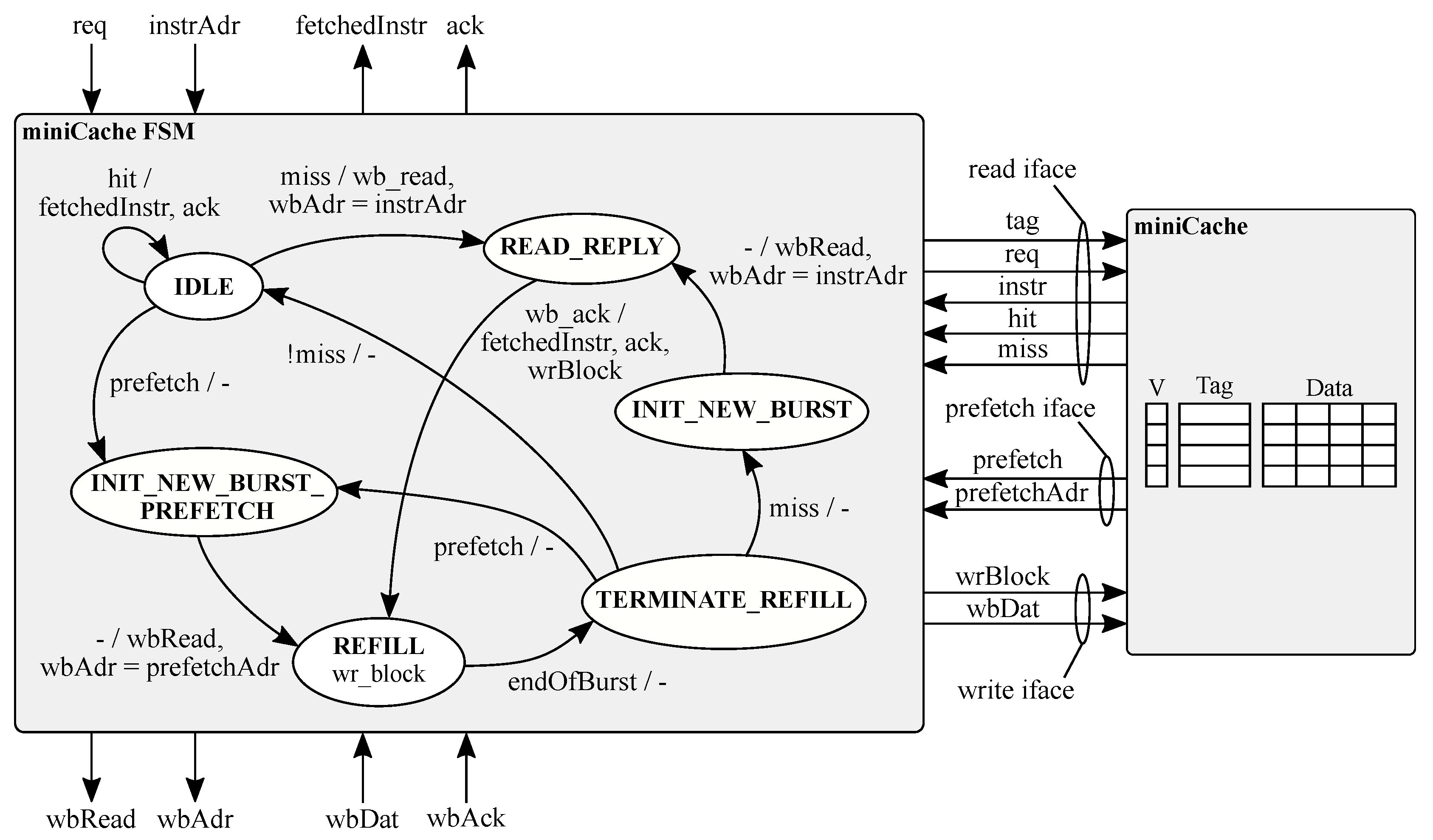
The instruction cache in the form of a regular cache or a FIFO queue represents the second analyzed microarchitectural component. As the instruction cache strongly supports the CPU performance, its use can severely affect both area and timing. To this extent, the use of either a small cache or even no instruction cache represents a common implementation strategy for several low- and high- end microcontrollers [33], e.g., ARM Cortex-M0, M3, M4, and M7. We explore the use of both a miniCache and a FIFO queue to boost the performance, still ensuring a limited impact on timing and area design metrics. The proposed instruction miniCache controller and cache memory are depicted in Figure 3 also showing the connecting signals to the instruction fetch and to the instruction bus. The proposed microarchitecture allows a combinational cache lookup. In the same clock cycle, either the data is returned, in case of a lookup hit, or a new Wishbone burst transaction is started to load the cache line containing the IF stage requested address. The miniCache is a 4-line, fully associative cache and each line contains four 32-bit instructions. The proposed miniCache implements a simple prefetcher that starts prefetching the four next instructions, i.e., the next cache line in program order, if the last loaded cache line that is currently accessed by the IF stage contains no branch nor jump instructions. It is worth noticing that the prefetch starts a separate Wishbone transaction to preload.
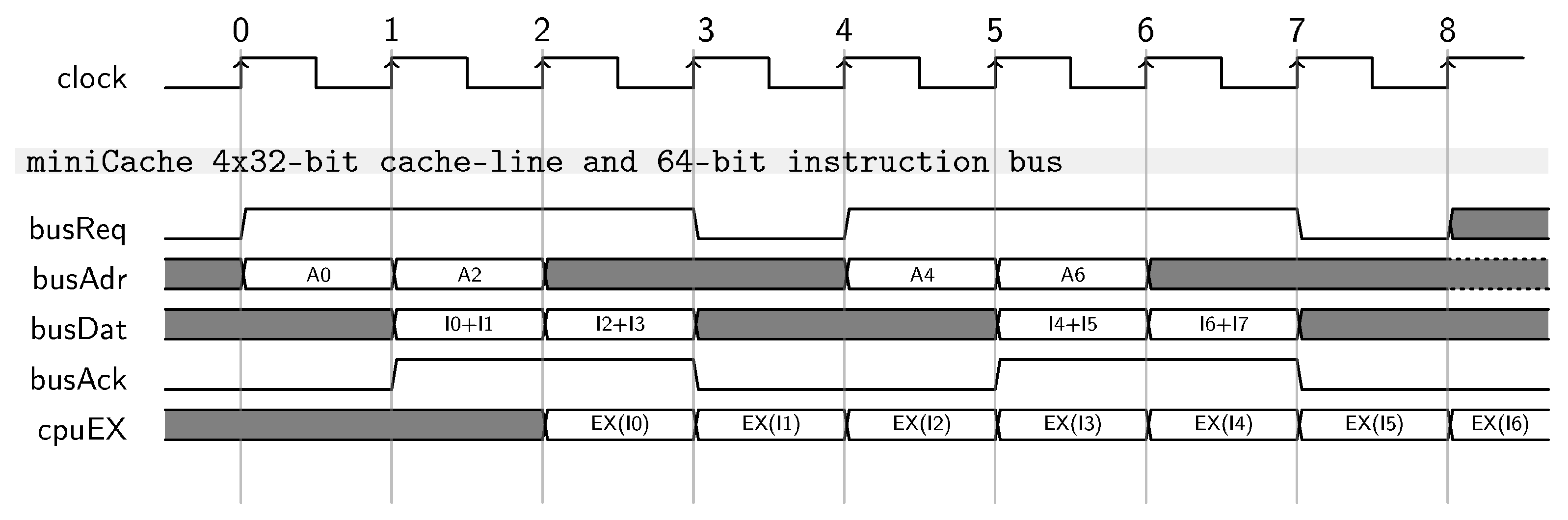
Starting from the proposed cache design, we highlight two different aspects that can severely degrade the overall CPU performance. First, the miniCache must finish refilling an entire cache line before start fetching a new line. This is a general rule for any cache design regardless its actual size. Second, the Wishbone communication protocol, and in general any on-chip protocol (e.g., AMBA), impose to any master to free up the bus for an entire clock cycle at the end of each transaction. This allows another master to take control over the bus thus avoiding starvation issues. The combination of these two observations can severely affect the CPU performance if a cache miss happens during a cache-line refill. In this scenario, the IF stage must wait for the cache to close the current cache line refill and the additional idle bus cycle imposed by the on-chip communication protocol. We note that such scenario happens any time during a cache line refill where one of the fetched instructions is a predicted-taken branch. In light of these two observations, the proposed miniCache features a cache line made of four 32-bit words to trade the refill cost with the need to completely fetch a cache line even in case of a cache miss. Figure 4 shows a 3-clock cycle burst transaction to fetch 4 instructions considering a miniCache supported by a 64-bit instruction bus. Such configuration allows full throughput for the CPU while executing a sequence of single clock latency instructions, i.e., ALU instructions. Moreover, a cache miss during a cache-line refill suffers a maximum penalty limited to two clock cycles.
The instruction FIFO queue represents a low area overhead scheme to solve the performance problems identified in the miniCache. We designed an 8-instructions FIFO queue coupled with a simple stride prefetcher (see Figure 5). Similar to the miniCache, the FIFO queue offers a combinational lookup for any incoming request from the instruction fetch stage. To this extent, a fetch request can be resolved within the requesting clock cycle in case of a hit event. Otherwise a Wishbone burst transaction is started in the same clock cycle to completely refill the FIFO. The FIFO leverages on the program order execution property to optimize its performance. In particular, on a miss, the missing instructions and the seven subsequent ones are fetched. We note that the FIFO queue can better handle a branch missprediction during a FIFO refill action, since the refill transaction can be aborted in any time, thus minimizing the penalty to serve a request out of program order. Moreover, we coupled the FIFO with a simple prefetcher that starts a FIFO refill transaction when the last FIFO slot is accessed.
The FIFO features 8-instruction slots to guarantee CPU full throughput when a 64-bit instruction bus is implemented. and a flow of single cycle latency, i.e., ALU instructions, is executed without branches. Figure 6 shows the execution of two burst transactions according to the Wishbone specification considering 32- and 64-bit for the instruction bus. The use of a 32-bit instruction bus can force two stall cycles in the CPU between the end of the first burst and the beginning of the next one. The first stall is due to the Wishbone specification. For each master issuing two consecutive transactions on the bus, the Wishbone imposes an entire idle clock cycle to avoid starvation issues for the other masters. The second stall is due to the beginning of the new transaction for which the corresponding data will be available in the following clock cycle. In contrast, the use of a 64-bit instruction bus allows to fetch up to two instructions for each clock cycle, thus completely shadowing the delay that induce the stall cycles.
We note that from the architectural viewpoints the FIFO queue and the miniCache require the same amount of storage since despite the smaller data storage, the FIFO requires a tag address for each instruction slot. However, the detailed evaluation of the two schemes is discussed in Section 4.2.
4. Experimental Results
This section provides a detailed evaluation of the microarchitectural variations to the Instruction Fetch (IF) stage proposed in Section 3.1. Each microarchitectural variation is evaluated in terms of area, timing, and performance using the baseline microarchitecture presented in Section 3 as reference design. By using a common vanilla CPU implementation we can carefully identify pros and cons of each solution with respect to the FPGA-based hardware design flow. In particular, Table 2 reports the set of evaluated microarchitectures and the short names that are used in the rest of this part to name each one of them.
In addition, we defined the Best-uArch-gShare and the Worst-uArch-alwNT microarchitectures as the two extreme points in terms of offered performance. The Best-uArch-gShare represents our performance golden model. It implements a 32-bit instruction bus, a 32-entry gShare branch prediction scheme and a combinational instruction RAM to avoid any instruction fetch penalty. We note that the instruction bus width, i.e., 32 or 64-bit, does not affect the performance of Best-uArch-gShare since each instruction fetch request is completed within the requesting clock cycle. The Worst-uArch-alwNT represents the worst possible architecture implementing no caches nor branch prediction scheme and a 32-bit instruction bus. Each instruction fetch request starts a Wishbone single read transaction taking 2 clock cycles.
The proposed RISC-V CPU microarchitecture and all the variations have been described in SystemVerilog 2012 passing through the entire FPGA flow of synthesis and implementation and the final design has been tested on a Digilent Nexys 4 DDR board featuring a Xilinx Artix 100t FPGA chip. In particular, we constrained the clock frequency to 70MHz in the implementation to allow a shared operating frequency for all the evaluated microarchitectural variations. The validation of each CPU implementation has been carried out considering both ad-hoc benchmarks, to selectively stress portion of the design, as well as a set of 29 WCET benchmarks for which the taxonomy is reported in Table 3 [34]. The WCET benchmarks include a representative mix of algorithm-types from both embedded and general-purpose computing domains. The same benchmarks have been executed on an x86-64 laptop to check the computational correctness.
The rest of this section is organized in two parts. The performance results are reported in Section 4.1 for each microarchitecture defined in Table 3. Section 4.2 reports the area and timing results for the same set of microarchitectures.
4.1. Performance evaluation
This section reports the performance evaluation in terms of number of clock cycles to execute a benchmark considering each microarchitecture described in Table 2. Moreover, the Best-uArch-gShare and the Worst-uArch-alwNT are employed to bound optimal and worst performance results.
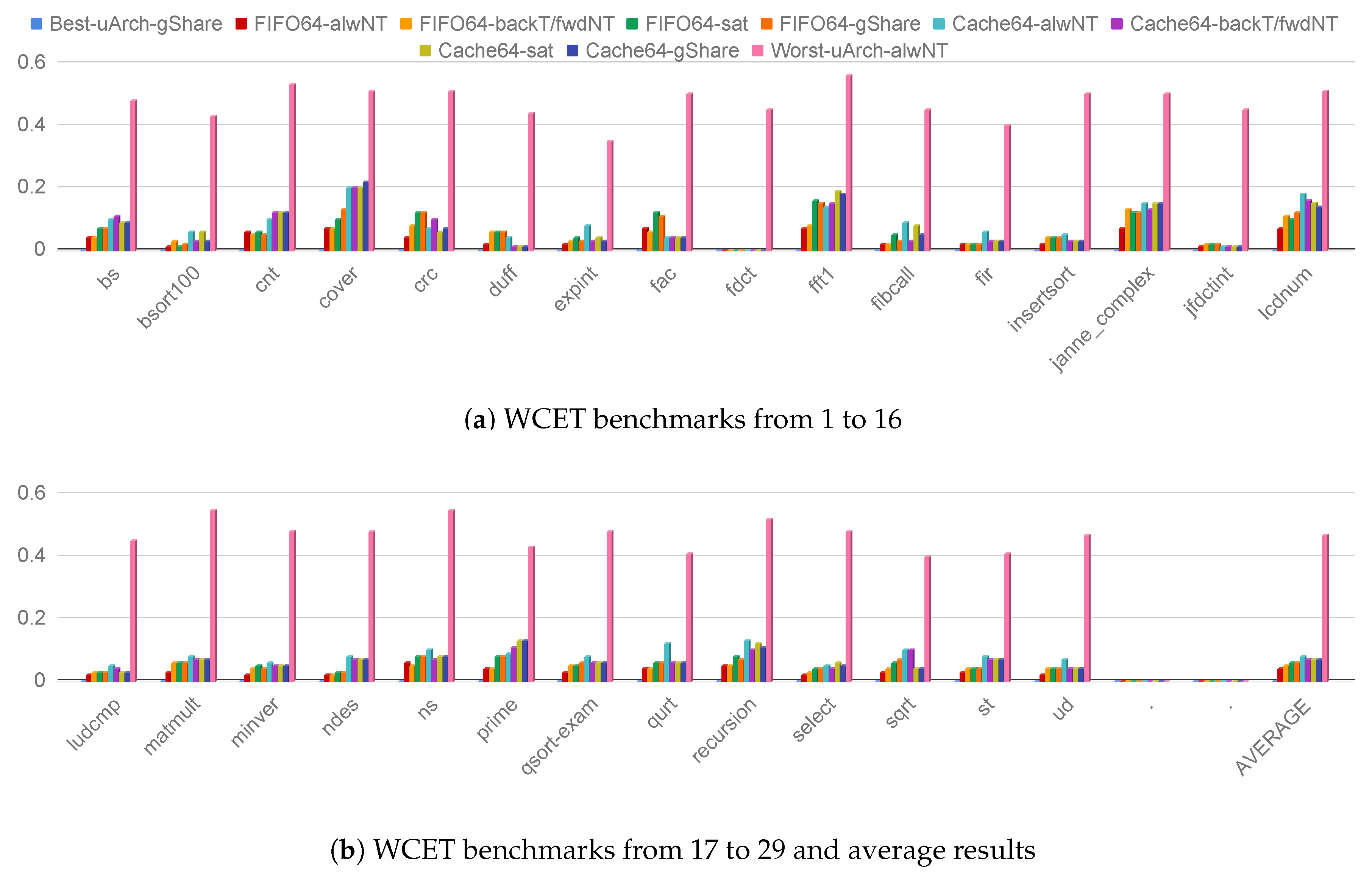
Branch prediction schemes. Considering an in-order processor, the performance of a branch prediction scheme, i.e., number of misspredicted branches, remains the same regardless the cache microarchitecture or the instruction bus width since it only depends on the program control-flow and its actual input data. To this extent, Figure 7 reports the number of branch misspredictions for all the considered microarchitectures on the 29 executed WCET benchmarks.
The always not taken (alwNT) branch predictor scheme offers the lower performance since no branch prediction capability is actually offered. Moreover, the gShare always overcomes the saturation (sat) scheme since the former implements a vector of sat branch predictors thus minimizing the probability that two different branches modify the internal state of the same saturation predictor. Last, the backward taken forward not taken (backT/FwdNT) branch predictor scheme offers reasonable performance despite its simplicity especially for loop-dominated applications. We note a few outliers to these set of rules, i.e., bsort100, cover, fibcall, expint, for which the saturation branch prediction scheme offers lower performance than the BackT/FwdNT one. From a careful analysis, we note an intricate application control-flow for which consecutive branches collide in the update of the internal state of a few saturation predictors.
Furthermore, cover shows poor performance for the gShare predictor. A careful exploration of the application behavior shows a gShare use below 20%. This means that different branch instructions update the same sat predictor, and the same sat predictor is used to predict their outcome. Moreover, the majority (80%) of the sat predictors implemented in the gShare are not used for the entire application execution. This behavior shifts the performance of the gShare close to the performance of the single sat branch predictor.
Performance and cache miss impact using a 32-bit instruction bus. For each microarchitecture and branch prediction scheme, Figure 8 and Figure 9 report the performance and the impact of the miss rate for the considered WCET applications. All the results are extracted using a 32-bit instruction bus. The performance results in Figure 8 are normalized to the Best-uArch-gShare microarchitecture, thus the smaller the numbers the better the performance. We note that the number of clock cycles due to the fetch misses is normalized to the total number of clock cycles to complete the execution of the specific application. To observe the performance impact due to the instruction cache misses, we account for the number of clock cycles for a miss and not only the number of instruction misses. In particular, two instruction misses can take a different number of clock cycles to be resolved. For example, an instruction miss takes longer when happens during a cache-line refill since the latter must be completed before the former can be served.
In contrast the use of a FIFO queue in place of the miniCache shows the performance improvement up to 10% (6.5% on average) due to two different observations. First, the FIFO queue can stop refilling when a branch is taken thus the next program counter is not loading the subsequent instruction, i.e., PC+4. In contrast the miniCache must complete the refill of an entire cache line before start serving the instruction fetch miss. Second, the FIFO implements an easier and more efficient prefetching scheme that starts fetching the next eight instructions in program order when the last slot, i.e., instruction, in the FIFO is accessed by the IF stage.
We also note that the applications with a low number of load/store or multicycle instructions (see Table 3), e.g., fft1 or cnt, show higher sensitivity to the microarchitecture of the instruction fetch stage. For these applications, the instruction fetch stage is greatly stressed by the few pipeline stalls imposed by the other pipeline stages. In this scenario the superior performance of the FIFO against the miniCache is magnified.
We also note that a few applications, e.g., fdct, jfdctint and insertsort, traverse a low number of branches, i.e., less than 3% of their instructions are branches (see Table 3), thus showing no performance variations due to the IF stage microarchitecture. In particular, these applications are not stressing the FIFO/Cache and the branch prediction scheme since they execute the instructions in program order.
Performance and cache miss impact using a 64-bit instruction bus. For each microarchitecture and branch prediction scheme, Figure 10 and Figure 11 report the performance and the impact of the miss rate for the considered WCET applications. All the results are extracted using a 64-bit instruction bus, while the microarchitecture is still a 32-bit one and the data bus width is fixed to 32-bits. The 64-bit bus allows fetching two instructions for each clock cycle thus reducing the latency of any Wishbone burst transaction. Such lower latency reduces the number of clock cycles to serve a miss when the miniCache is implemented (see Cache64- in Figure 11) due to faster cache-line refills. We note that the miniCache forces an instruction miss to wait until when the current cache-line refill, if any, is over before being served. In particular, the use of a 64-bit instruction bus (see Figure 10) in place of a 32-bit one (see Figure 8) allows a miniCache performance improvement up to 6% (5.25% on average). However, the FIFO still overcomes the miniCache when both are employing a 64-bit instruction bus (3.25% on average).
4.2. Area and Timing Evaluation
This section discusses area and timing results considering the microarchitectures reported in Table 2. Table 4 reports the area overhead in terms of LUT and flip flop counts. All the results are normalized with respect to the Worst-uArch-alwNT.
We note that the area overhead for LUT and flip-flops is limited to 9% and 3%, respectively, since the numbers are averaged on the entire CPU occupation. While the flip-flop overhead is limited the LUT one can be as high as 9% of the entire CPU.
In particular, the LUT overhead mostly depends on the use of a FIFO or a miniCache and stays independent from the instruction bus width. Moreover, the LUT overhead is not directly related to the size of the cache but depends on the additional logic to implement the replacement policy. We note that the miniCache implements a FIFO replacement. The gShare branch predictor scheme shows a similar relationship with the LUT overhead due to the additional decoding logic used to access and update the list of saturation predictors.
Table 5 reports the timing slack for the considered implementations using a 70 MHz clock frequency. For each microarchitecture the absolute timing slack is reported in nanoseconds and as normalized value with respect to Worst-uArch-alwNT microarchitecture.
We note that the timing slack is mostly affected by the employed branch prediction scheme while there is no clear evidence of a worse or better scheme with respect to the timing slack design metric. For example, the gShare shows a timing slack of 0.88 ns and 0.22 ns when used within the Cache32-gShare and FIFO32-gShare architectures, respectively (see Table 5). A careful analysis for each microarchitecture at the post-implementation stage highlights that the timing variations are not due to a more or less complex logic within different branch predictors or cache implementations. In contrast, such timing slack difference is primarily due to net delays, i.e., the geometry placement of the different cells during the place and route (PAR) stage of the hardware design flow. We note that such numbers are, then, perfectly aligned with the implemented heuristics to fulfill the PAR stage. As soon as the PAR algorithm finds an implementation instance that meets all the timing and physical constraints the algorithm stops executing and such solution is returned. The choice to constrain the operating frequency at 70 MHz leaves a decent timing slack to avoid routing congestion and logic duplication to optimize the fan-out still ensuring that the post-implementation timing slack stays within 10% of the imposed clock period, i.e., around 14 ns at 70 MHz.
To summarize, the results in Table 5 report a similar timing slack for all the considered configurations.
5. FPGA-Based Design Suggestions for IoT CPUs
The goal of this part is two-fold. First, we aim to deliver a final performance comparison between the best microarchitectures employing a FIFO queue and a miniCache with a regular set-associative instruction cache. Second, we deliver a set of three design guidelines to design the front-end of IoT CPU for FPGA implementation.
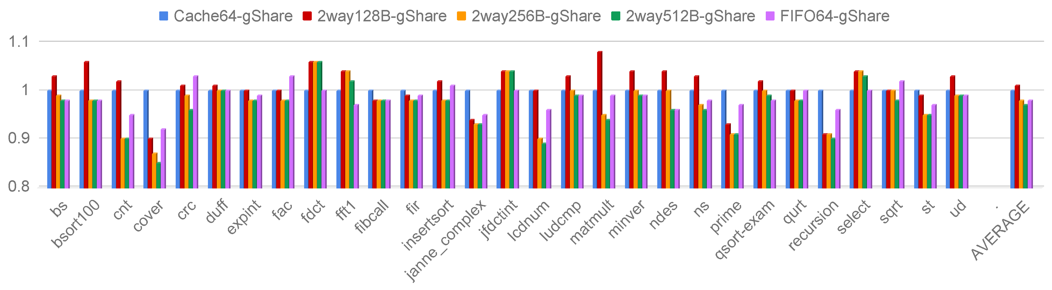
Performance comparison with a set-associative instruction cache. The regular set-associative instruction cache represents a standard architectural component used in high-end embedded systems to sustain performance. Considering FPGA implementations of RISC CPUs the use of a regular cache imposes the use of Block RAM (BRAM) primitives as cache memory instead of the regular flip-flop cells since the latter are a scarce FPGA resource. In particular, Xilinx BRAMs are synchronous primitives thus their use shows a performance penalty for each cache access even in case of a hit. To allow a fair comparison between the miniCache and the FIFO, we implemented a flip-flop-based regular set-associative cache featuring a 2-way per set architecture where each cache line contains 4 32-bit instructions. Such configuration allows a successful implementation at 70 MHz. We note that our goal is to assess the required regular cache size to match or even to overcome the performance of the proposed instruction FIFO queue.
Figure 12 reports the performance results considering 3 sizes for the regular set-associative cache, i.e., 4 cache lines (2way128B-gShare), 8 cache lines (2way256B-gShare) and 16 cache lines (2way512B-gShare). Moreover, the results for the best FIFO and miniCache configurations from Section 4, i.e., FIFO64-gShare and Cache64-gShare are also reported for comparison purposes. All the evaluated microarchitectures, i.e., miniCache, FIFO and regular cache, employ the 64-bit instruction bus and the gShare branch prediction scheme. The results are normalized to the Cache64-gShare microarchitecture.
The regular cache featuring 2048-bit memory, i.e., 2way512B-gShare, cannot overcome the performance of the FIFO queue by more than 8% for all the considered benchmarks. For example, lcdnum show a performance improvement limited to 8% when a regular cache (2way512B-gShare) is used in place of the FIFO queue. However, the 2way512B-gShare features 8-time bigger data storage than FIFO64-gShare. Moreover, the proposed standard instruction cache sits on a flip-flop implementation to allow a combinational cache lookup. The use of a flip-flop implementation severely limits the maximum size of the standard cache due to the limited number of available flip-flops on the FPGA chip. As already stated, the alternative solution is the use of BRAM ad-hoc memory resources that, however, critically affect the overall CPU performance.
Design guidelines. Starting from the results presented in Section 4 and Section 5, we formalize three design guidelines:
- Guidelines 1: FIFO for area constrained designs. The instruction FIFO represents the best design choice when the area overhead is critical. It offers good performance due to its high flexibility that permits to abort a burst transaction and start serving an instruction miss. Moreover, the simple prefetch scheme offers a full-throughput pipeline if the instructions are executed in program order. In particular, it always offers superior performance compared to a miniCache. By contrast, the use of a bigger standard cache coupled with a 64-bit instruction bus can offer better performance in a multi-master platform.
- Guidelines 2: use 64-bit instruction bus on 32-bit architectures. The use of a 64-bit instruction bus offers superior performance by dramatically reducing the latency of any on-chip burst transaction. Moreover, the implementation results demonstrated a negligible impact on both timing and area design metrics. Last, a wider bus reduces the contention in multi-master platforms.
- Guidelines 3: Branch prediction scheme. We note that the branch prediction scheme greatly improves the overall performance even if the scheme is as simple as the backT/FwdNT one. In particular, the selected branch predictor scheme can marginally affect the area while the reported timing slack is not dominated by a specific scheme. To this extent, we suggest the use of a backT/FwdNT scheme for area constrained designs or a more capable gShare with a small number of saturation predictors. We also note that it is always important to check the percentage of actually used saturation predictors implemented in the gShare scheme to avoid wasting resources.
6. Conclusions
The IoT revolution shaped a new application domain where the low-power RISC architectures constitute the standard computational backbone. The current de-facto practice is to extend the ISA with custom instruction sets to efficiently manage the complex tasks imposed by IoT applications, i.e., augmented reality, artificial intelligence, and autonomous driving, within narrow energy and area budgets. However, we think that the newly IoT applications offers a unique opportunity to revisit and optimize the RISC microarchitectural design flow from a more communication- and memory-centric viewpoint.
From this perspective, the manuscript proposed a complete exploration and optimization of the microarchitecture of a RISC CPU front-end considering area timing and performance design metrics.
The analysis has leveraged a newly developed SoC and RISC CPU compliant with the RISC-V IMF ISA standard extensions. The complete design acts as reference design to isolate pros and cons of each evaluated microarchitectural change. The proposed SoC has been implemented and validation on a prototype Xilinx Artix 7 100t FPGA chip with a clock frequency set at 70 MHz.
The extracted results highlight the possibility of using a 64-bit instruction bus on a 32-bit architecture to boost the performance by ensuring low cache-line refill latency. Moreover, we note that the use of a FIFO queue in place of a standard instruction cache ensures great performance advantages with low area overhead and no timing penalty. Last, the use of a complex branch predictor show good performance results with minimal area overhead and no timing overhead. All the microarchitectural observations emerged from the analysis have been carefully shaped in a set of three guidelines to steer the microarchitectural design of RISC CPU for IoT platforms.
Author Contributions
Investigation, G.S. and D.Z.; Methodology, D.Z.; Supervision, D.Z.
Funding
This work was partially supported by two EU grants within the EU H2020 Research and Innovation Programme: “MANGO” Grant agreement no. 671668 and “RECIPE” Grant agreement no. 801137.
Conflicts of Interest
The authors declare no conflict of interest.
References
- Piazza, E.; Romanoni, A.; Matteucci, M. Real-Time CPU-Based Large-Scale Three-Dimensional Mesh Reconstruction. IEEE Rob. Autom. Lett. 2018, 3, 1584–1591. [Google Scholar] [CrossRef] [Green Version]
- Romanoni, A.; Ciccone, M.; Visin, F.; Matteucci, M. Multi-view Stereo with Single-View Semantic Mesh Refinement. In Proceedings of the IEEE International Conference on Computer Vision Workshops (ICCVW), Venice, Italy, 22–29 October 2017; pp. 706–715. [Google Scholar]
- Romanoni, A.; Fiorenti, D.; Matteucci, M. Mesh-based 3D textured urban mapping. In Proceedings of the IEEE/RSJ International Conference on Intelligent Robots and Systems (IROS), Vancouver, BC, Canada, 24–28 September 2017; pp. 3460–3466. [Google Scholar]
- Hennessy, J.; Patterson, D. A new golden age for computer architecture: Domain-specific hardware/software co-design, enhanced security, open instruction sets, and agile chip development. In Proceedings of the 2018 ACM/IEEE 45th Annual International Symposium on Computer Architecture (ISCA), Los Angeles, CA, USA, 1–6 June 2018; pp. 27–29. [Google Scholar]
- Foundation, R.V. RISC-V Instruction Set Architecture (ISA). Available online: https://riscv.org/ (accessed on 19 Feburary 2019).
- Zoni, D.; Colombo, L.; Fornaciari, W. DarkCache: Energy-Performance Optimization of Tiled Multi-Cores by Adaptively Power-Gating LLC Banks. ACM Trans. Archit. Code Optim. 2018, 15, 21:1–21:26. [Google Scholar] [CrossRef]
- Zoni, D.; Flich, J.; Fornaciari, W. CUTBUF: Buffer Management and Router Design for Traffic Mixing in VNET-Based NoCs. IEEE Trans. Parallel Distrib. Syst. 2016, 27, 1603–1616. [Google Scholar] [CrossRef]
- Zoni, D.; Canidio, A.; Fornaciari, W.; Englezakis, P.; Nicopoulos, C.; Sazeides, Y. BlackOut: Enabling fine-grained power gating of buffers in Network-on-Chip routers. J. Parallel Distrib. Comput. 2017, 104, 130–145. [Google Scholar] [CrossRef] [Green Version]
- arm Ltd. Designstart FPGA. Available online: https://www.arm.com/resources/designstart/designstart-fpga (accessed on 19 Feburary 2019).
- Patsidis, K.; Konstantinou, D.; Nicopoulos, C.; Dimitrakopoulos, G. A low-cost synthesizable RISC-V dual-issue processor core leveraging the compressed Instruction Set Extension. Microprocess. Microsyst. 2018, 61, 1–10. [Google Scholar] [CrossRef]
- Conti, F.; Rossi, D.; Pullini, A.; Loi, I.; Benini, L. PULP: A Ultra-Low Power Parallel Accelerator for Energy-Efficient and Flexible Embedded Vision. J. Signal Process. Syst. 2016, 84, 339–354. [Google Scholar] [CrossRef]
- openrisc. Mor1kx Project. 2016. Available online: https://github.com/openrisc/mor1kx (accessed on 19 February 2019).
- Project, O. OpenRISC Reference Platform SoC Version 3. 2016. Available online: https://github.com/fusiled/ORPSocv3 (accessed on 19 February 2019).
- Asanović, K.; Avizienis, R.; Bachrach, J.; Beamer, S.; Biancolin, D.; Celio, C.; Cook, H.; Dabbelt, D.; Hauser, J.; Izraelevitz, A.; et al. The Rocket Chip Generator; Technical Report UCB/EECS-2016-17; EECS Department, University of California: Berkeley, CA, USA, 2016. [Google Scholar]
- VectorBlox. Orca Core. Available online: https://github.com/vectorblox/orca (accessed on 19 February 2019).
- Celio, C.; Patterson, D.A.; Asanović, K. The Berkeley Out-of-Order Machine (BOOM): An Industry-Competitive, Synthesizable, Parameterized RISC-V Processor; Technical Report UCB/EECS-2015-167; EECS Department, University of California: Berkeley, CA, USA, 2015. [Google Scholar]
- Celio, C.; Chiu, P.F.; Nikolic, B.; Patterson, D.A.; Asanović, K. BOOM v2: An Open-Source Out-of-Order RISC-V Core; Technical Report UCB/EECS-2017-157; EECS Department, University of California: Berkeley, CA, USA, 2017. [Google Scholar]
- VexRiscv Core. SpinalHDL. 2017. Available online: https://github.com/SpinalHDL/VexRiscv (accessed on 19 February 2019).
- Gray, J. GRVI Phalanx: A Massively Parallel RISC-V FPGA Accelerator. In Proceedings of the 2016 IEEE 24th Annual International Symposium on Field-Programmable Custom Computing Machines (FCCM), Washington, DC, USA, 1–3 May 2016; pp. 17–20. [Google Scholar]
- OpenRISC 1000 Architectural Manual. Available online: https://openrisc.io/or1k.html (accessed on 19 Feburary 2019).
- Kristiansson, S. Bare-Metal Introspection Application for the AR100 Controller of Allwinner A31 SoCs. Available online: https://github.com/skristiansson/ar100-info (accessed on 19 Feburary 2019).
- Linux Kernel OpenRISC Subtree. Available online: https://github.com/kdgwill/OR1K/wiki/Build-Linux-Kernel-For-OpenRisc-1000 (accessed on 19 Feburary 2019).
- Kurth, A.; Vogel, P.; Capotondi, A.; Marongiu, A.; Benini, L. HERO: Heterogeneous Embedded Research Platform for Exploring RISC-V Manycore Accelerators on FPGA. arXiv, 2017; arXiv:1712.06497. [Google Scholar]
- Davidson, S.; Xie, S.; Torng, C.; Al-Hawai, K.; Rovinski, A.; Ajayi, T.; Vega, L.; Zhao, C.; Zhao, R.; Dai, S.; et al. The Celerity Open-Source 511-Core RISC-V Tiered Accelerator Fabric: Fast Architectures and Design Methodologies for Fast Chips. IEEE Micro 2018, 38, 30–41. [Google Scholar] [CrossRef]
- Eldridge, S.; Swaminathan, K.; Verma, V.; Joshi, R. A Low Voltage RISC-V Heterogeneous System Boosted SRAMs, Machine Learning, and Fault Injection on VELOUR. 2017. Available online: https://pdfs.semanticscholar.org/608e/831e8ab14c0e5700eb5f3a01cc054b0d663e.pdf (accessed on 19 February 2019).
- onchipuis. mriscv. Available online: https://github.com/onchipuis/mriscv (accessed on 19 February 2019).
- Matthews, E.; Shannon, L. Taiga: A configurable RISC-V soft-processor framework for heterogeneous computing systems research. In Proceedings of the First Workshop on Computer Architecture Research with RISC-V (CARRV 2017), Boston, MA, USA, 14 October 2017. [Google Scholar]
- Binkert, N.; Beckmann, B.; Black, G.; Reinhardt, S.K.; Saidi, A.; Basu, A.; Hestness, J.; Hower, D.R.; Krishna, T.; Sardashti, S.; et al. The Gem5 Simulator. SIGARCH Comput. Archit. News 2011, 39, 1–7. [Google Scholar] [CrossRef]
- Zoni, D.; Fornaciari, W. Modeling DVFS and Power Gating Actuators for Cycle Accurate NoC-based Simulators. J. Emerg. Technol. Comput. Syst. 2015, 12, 1–15. [Google Scholar] [CrossRef]
- Zoni, D.; Terraneo, F.; Fornaciari, W. A DVFS Cycle Accurate Simulation Framework with Asynchronous NoC Design for Power-Performance Optimizations. J. Signal Process. Syst. 2016, 83, 357–371. [Google Scholar] [CrossRef]
- OpenCores. Wishbone System-on-Chip (SoC) Interconnection Architecture for Portable IP Cores. Available online: http://docplayer.net/6521799-Wishbone-system-on-chip-soc-interconnection-architecture-for-portable-ip-cores.html (accessed on 2 Feburary 2019).
- Patterson, D.A.; Hennessy, J.L. Computer Organization and Design—The Hardware/Software Interface, 4th ed.; The Morgan Kaufmann Series in Computer Architecture and Design; Academic Press: New York, NY, USA, 2012. [Google Scholar]
- Martin, T. The Designer’s Guide to the Cortex-M Processor Family, 2nd ed.; Elsevier: Amsterdam, The Netherlands, 2016. [Google Scholar]
- Gustafsson, J.; Betts, A.; Ermedahl, A.; Lisper, B. The Malardalen WCET Benchmarks: Past, Present and Future. In Proceedings of the 10th International Workshop on Worst-Case Execution Time Analysis, Brussels, Belgium, 6 July 2010. [Google Scholar]
Figure 1.
Schematic view of the proposed system-on-chip. A 5-stage RISC CPU implementing the RISC-V/IMF ISA is used as reference design. A physically split (data and instruction) Wishbone bus implementing both simple and burst transactions is used as on-chip interconnect. Two slaves, i.e., the RAM and the UART complete the SoC allowing complete observability for user program on the prototype FPGA-based board. Last, the global (duGlobal) and local (duLocal) debuggers allow to load the binary and control the CPU execution on the prototype FPGA-based board by offering GDB-like commands.

Figure 2.
Schematic view of the branch prediction scheme. At design time it is possible to select the scheme to implement (see resolved at impl. time multiplexer). Each saturation branch predictor in the gShare model features the classical four state finite state machine (FSM), i.e., taken (T), weakly taken (WT), weakly not taken (WNT), not taken (NT). The FSM is updated by the signal reporting branch taken (BT) or branch not taken (BNT). Such signal is generated during the evaluation of the branch in the EX pipeline stage.

Figure 3.
Schematic view of the instruction miniCache microarchitecture.

Figure 4.
The use of a 64-bit instruction bus combined with the miniCache allows to completely shadow the idle cycles between two consecutive transactions imposed by the Wishbone specification. Such implementation allows full throughput for the CPU that is processing a stream of single cycle latency instructions without control instructions in the between.

Figure 5.
Schematic view of the instruction FIFO microarchitecture.

Figure 6.
The use of a 64-bit instruction bus combined with an 8-slot FIFO allows to completely shadow the idle cycles between two consecutive transactions imposed by the Wishbone specification. Such implementation allows full throughput for the CPU that is processing a stream of single cycle latency instructions without control instructions in the between.

Figure 7.
Misprediction rate for the evaluated branch predictor schemes. Results are normalized with respect to the total number of branch instructions (see Table 3).
Figure 7.
Misprediction rate for the evaluated branch predictor schemes. Results are normalized with respect to the total number of branch instructions (see Table 3).

Figure 8.
Normalized execution time using a 32-bit instruction bus width. The microarchitectural combinations described in Table 2 are considered. Results are normalized to Best-uArch-gShare.
Figure 8.
Normalized execution time using a 32-bit instruction bus width. The microarchitectural combinations described in Table 2 are considered. Results are normalized to Best-uArch-gShare.

Figure 9.
Number of clock cycle delay due to instruction fetch miss using a 32-bit instruction bus. The microarchitectural combinations described in Table 2 are considered. Each result is normalized to the corresponding total number of executed clock cycles.
Figure 9.
Number of clock cycle delay due to instruction fetch miss using a 32-bit instruction bus. The microarchitectural combinations described in Table 2 are considered. Each result is normalized to the corresponding total number of executed clock cycles.

Figure 10.
Normalized execution time using a 64-bit instruction bus width. The microarchitectural combinations described in Table 2 are considered. Results are normalized to Best-uArch-gShare.
Figure 10.
Normalized execution time using a 64-bit instruction bus width. The microarchitectural combinations described in Table 2 are considered. Results are normalized to Best-uArch-gShare.

Figure 11.
Number of clock cycle delay due to instruction fetch miss using a 64-bit instruction bus. The microarchitectural combinations described in Table 2 are considered. Each result is normalized to the corresponding total number of executed clock cycles.
Figure 11.
Number of clock cycle delay due to instruction fetch miss using a 64-bit instruction bus. The microarchitectural combinations described in Table 2 are considered. Each result is normalized to the corresponding total number of executed clock cycles.

Figure 12.
Normalized execution time using a 64-bit instruction bus width and the best configurations for miniCache and FIFO as well as a 2-way set-associative instruction cache with different parameters. Results are normalized with respect to the Cache64-gShare microarchitecture.
Figure 12.
Normalized execution time using a 64-bit instruction bus width and the best configurations for miniCache and FIFO as well as a 2-way set-associative instruction cache with different parameters. Results are normalized with respect to the Cache64-gShare microarchitecture.


Table 1.
Open-hardware CPUs and relative key microarchitectural attributes.
| Core | ISA | Pipeline Stages | Out-of-Order | Issue Width | Caches | Branch Prediction |
|---|---|---|---|---|---|---|
| Mor1kx Cappuccino [12] | OpenRISC | 5 | in-order | 1 | yes | no |
| Mor1kx Espresso [12] | OpenRISC | 3 | in-order | 1 | no | no |
| Mor1kx ProntoEspresso [12] | OpenRISC | 3 | in-order | 1 | no | yes |
| ORPSoC v3 [13] | OpenRISC | 5 | in-order | 1 | yes | yes |
| Rocket [14] | RV32/64/IMAFD | 5 | in-order | 1 | yes | yes |
| ORCA [15] | RV32/IM | 4,5 | in-order | 1 | no | no |
| BOOM v1 [16] | RV64/IMAFD | 6 | out-of-order | up to 3 | yes | yes |
| BOOM v2 [17] | RV64/IMAFD | 6 | out-of-order | up to 4 | yes | yes |
| PULP Ariane [11] | RV32/IMF | 6 | in-order | 1 | yes | yes |
| PULPino [18] | RV32/IMCF | 4 | in-order | 1 | yes (+FIFO) | no |
| VexRiscv [19] | RV32IM | 5 | in-order | 1 | yes | no |
| mriscv [11] | RV32/I | 3 | in-order | 1 | no | no |
| dualIssueRiscv [10] | RV32/IMCF | 6 | in-order | up to 2 | yes | yes |
Table 2.
Taxonomy of the different microarchitectures explored in this work for which results are reported. A label is assigned to each combination of branch prediction scheme, instruction bus width and the use of an instruction FIFO or a miniCache.
Table 2.
Taxonomy of the different microarchitectures explored in this work for which results are reported. A label is assigned to each combination of branch prediction scheme, instruction bus width and the use of an instruction FIFO or a miniCache.
| Instruction Bus 32 bit | Instruction Bus 64 bit | |||
|---|---|---|---|---|
| Instruction FIFO | Instruction Cache | Instruction FIFO | Instruction Cache | |
| always not taken | FIFO32-alwNT | Cache32-alwNT | FIFO64-alwNT | Cache64-alwNT |
| backward taken forward not taken | FIFO32-BackT/FwdNT | Cache32-BackT/FwdNT | FIFO64-BackT/FwdNT | Cache64-BackT/FwdNT |
| saturation | FIFO32-sat | Cache32-sat | FIFO64-sat | Cache64-sat |
| gShare | FIFO32-gShare | Cache32-gShare | FIFO64-gShare | Cache64-gShare |
Table 3.
WCET applications employed in our evaluation. For each benchmark the total number of executed instructions is reported considering the FIFO 32 implementation with the always not taken static branch prediction scheme. Moreover, the mix of instruction types and the number of taken branches are also reported.
| Benchmark | Total # of | # of Taken | Number of Instructions Per Type (%) | ||||||
|---|---|---|---|---|---|---|---|---|---|
| Instructions | Branch | Branch | Jump | ALU | NOP | MUL/DIV | FPU | LD/ST | |
| bs | 158 | 8 | 7.5 | 3.8 | 32.2 | 9.4 | 0.0 | 0.0 | 46.8 |
| bsort100 | 251,516 | 5452 | 6.2 | 0.0 | 38.5 | 2.2 | 0.0 | 0.0 | 52.8 |
| cnt | 7575 | 220 | 4.5 | 4.3 | 62.1 | 7.2 | 1.3 | 0.0 | 20.3 |
| cover | 4222 | 180 | 8.6 | 8.7 | 34.8 | 13.0 | 0.0 | 0.0 | 34.7 |
| crc | 56,028 | 3493 | 8.5 | 3.2 | 41.1 | 9.4 | 0.0 | 0.0 | 37.6 |
| duff | 2149 | 105 | 5.0 | 0.2 | 33.5 | 5.5 | 0.0 | 0.0 | 55.6 |
| expint | 3714 | 151 | 6.8 | 2.8 | 20.8 | 6.9 | 8.1 | 0.0 | 54.4 |
| fac | 527 | 21 | 5.3 | 9.3 | 29.9 | 13.2 | 2.8 | 0.0 | 39.2 |
| fdct | 5305 | 16 | 0.3 | 0.0 | 44.5 | 0.4 | 3.6 | 0.0 | 50.9 |
| fft1 | 55,939 | 3065 | 9.8 | 4.1 | 58.8 | 10.6 | 3.2 | 1.3 | 12.0 |
| fibcall | 562 | 30 | 10.5 | 0.5 | 17.9 | 5.8 | 0.0 | 0.0 | 65.1 |
| fir | 478,682 | 25,541 | 5.4 | 0.1 | 20.5 | 5.4 | 5.2 | 0.0 | 63.1 |
| insertsort | 2052 | 54 | 3.1 | 0.4 | 53.5 | 3.1 | 0.0 | 0.0 | 39.7 |
| janne_complex | 398 | 40 | 15.0 | 2.0 | 26.1 | 12.0 | 0.0 | 0.0 | 44.7 |
| jfdctint | 5548 | 80 | 1.5 | 0.0 | 44.3 | 1.5 | 4.6 | 0.0 | 47.8 |
| lcdnum | 302 | 15 | 8.6 | 6.9 | 31.7 | 11.9 | 0.0 | 0.0 | 40.7 |
| ludcmp | 6113 | 213 | 4.7 | 1.1 | 39.4 | 4.6 | 5.0 | 4.9 | 39.9 |
| matmult | 9133 | 215 | 2.8 | 1.6 | 70.3 | 4.1 | 1.9 | 0.0 | 19.1 |
| minver | 4880 | 145 | 4.6 | 1.4 | 48.5 | 4.5 | 0.3 | 3.2 | 37.1 |
| ndes | 106,484 | 3437 | 4.4 | 3.0 | 41.6 | 6.2 | 0..0 | 0.0 | 44.6 |
| ns | 23,321 | 1404 | 6.6 | 0.6 | 58.4 | 6.7 | 0.0 | 0.0 | 27.4 |
| prime | 13,508 | 863 | 6.4 | 6.4 | 25.9 | 12.8 | 6.4 | 0.0 | 41.8 |
| qsort-exam | 2078 | 80 | 6.5 | 2.3 | 38.4 | 6.8 | 0.0 | 3.4 | 42.4 |
| qurt | 1205 | 93 | 9.2 | 3.7 | 14.6 | 11.4 | 0.0 | 16.6 | 44.2 |
| recursion | 4960 | 241 | 6.6 | 9.4 | 33.0 | 14.2 | 0.0 | 0.0 | 36.6 |
| select | 1033 | 31 | 6.0 | 1.0 | 44.0 | 4.1 | 0.0 | 2.6 | 42.1 |
| sqrt | 451 | 38 | 11.1 | 3.9 | 13.7 | 12.6 | 0.0 | 15.7 | 42.7 |
| st | 254,551 | 7156 | 2.8 | 4.7 | 31.5 | 7.6 | 1.5 | 12.8 | 38.7 |
| ud | 5855 | 207 | 4.7 | 0.9 | 42.0 | 4.5 | 7.0 | 0.0 | 40.6 |
Table 4.
Area overhead (LUT/Flip-Flops) for the implementation of the reference RISC core employing different combination of instruction bus width, branch prediction schemes and instruction cache type. Results are normalized to the implementation featuring a 32 bit instruction bus with an instruction FIFO and an always not taken static branch prediction scheme.
| Instruction Bus Width 32 bit | |||||||
|---|---|---|---|---|---|---|---|
| Instruction FIFO | Instruction Cache | ||||||
| Always Not Taken | Backward Taken Forward Not Taken | Saturation | gShare | Always Not Taken | Backward Taken Forward Not Taken | Saturation | gShare |
| 1.00/1.00 | 1.01/1.00 | 1.01/1.00 | 1.02/1.01 | 1.05 /1.02 | 1.08/1.02 | 1.06/1.02 | 1.09/1.02 |
| Instruction Bus Width 64 bit | |||||||
| Instruction FIFO | Instruction Cache | ||||||
| Always Not Taken | Backward Taken Forward Not Taken | Saturation | gShare | Always Not Taken | Backward Taken | Saturation Forward Not Taken | gShare |
| 1.01/0.99 | 1.01/0.99 | 1.01/0.99 | 1.03/1.00 | 1.06/1.02 | 1.07/1.02 | 1.07/1.02 | 1.08/1.03 |
Table 5.
Timing slack (absolute ns/normalized to FIFO32-alwNT) for the implementation of the reference RISC core employing different combinations of instruction bus width, branch prediction schemes and instruction cache type. Results are normalized to the implementation featuring a 32-bit instruction bus with an instruction FIFO and an always not taken static branch prediction scheme.
| Instruction Bus Width 32 bit | |||||||
|---|---|---|---|---|---|---|---|
| Instruction FIFO | Instruction Cache | ||||||
| Always Not Taken | Backward Taken Forward Not Taken | Saturation | gShare | Always Not Taken | Backward Taken Forward Not Taken | Saturation | gShare |
| 1.81 (1.00) | 0.27 (0.15) | 0.74 (0.41) | 0.22 (0.12) | 2.10 (1.16) | 0.90 (0.49) | 0.47 (0.26) | 0.88 (0.49) |
| Instruction Bus Width 64 bit | |||||||
| Instruction FIFO | Instruction Cache | ||||||
| Always Not Taken | Backward Taken Forward Not Taken | Saturation | gShare | Always Not Taken | Backward Taken Forward Not Taken | Saturation | gShare |
| 1.91 (1.05) | 0.23 (0.12) | 0.78 (0.43) | 0.62 (0.34) | 2.11 (1.17) | 0.84 (0.46) | 0.80 (0.44) | 0.50 (0.27) |
© 2019 by the authors. Licensee MDPI, Basel, Switzerland. This article is an open access article distributed under the terms and conditions of the Creative Commons Attribution (CC BY) license (http://creativecommons.org/licenses/by/4.0/).
Share and Cite
MDPI and ACS Style
Scotti, G.; Zoni, D. A Fresh View on the Microarchitectural Design of FPGA-Based RISC CPUs in the IoT Era. J. Low Power Electron. Appl. 2019, 9, 9. https://0-doi-org.brum.beds.ac.uk/10.3390/jlpea9010009
AMA Style
Scotti G, Zoni D. A Fresh View on the Microarchitectural Design of FPGA-Based RISC CPUs in the IoT Era. Journal of Low Power Electronics and Applications. 2019; 9(1):9. https://0-doi-org.brum.beds.ac.uk/10.3390/jlpea9010009
Chicago/Turabian StyleScotti, Giovanni, and Davide Zoni. 2019. "A Fresh View on the Microarchitectural Design of FPGA-Based RISC CPUs in the IoT Era" Journal of Low Power Electronics and Applications 9, no. 1: 9. https://0-doi-org.brum.beds.ac.uk/10.3390/jlpea9010009
Note that from the first issue of 2016, this journal uses article numbers instead of page numbers. See further details here.