Article

A Novel Single-Switch Single-Stage LED Driver with Power Factor Correction and Current Balancing Capability

1
Department of Electrical Engineering, National Formosa University, Hu-Wei, Yunlin 63201, Taiwan
2
Department of Electrical Engineering, I-Shou University, Kaohsiung 84001, Taiwan
*
Author to whom correspondence should be addressed.
Submission received: 6 May 2021 / Revised: 31 May 2021 / Accepted: 31 May 2021 / Published: 3 June 2021

Abstract

:
A novel single-switch single-stage high power factor LED driver is proposed by integrating a flyback converter, a buck–boost converter and a current balance circuit. Only an active switch and a corresponding control circuit are used. The LED power can be adjusted by the control scheme of pulse–width modulation (PWM). The flyback converter performs the function of power factor correction (PFC), which is operated at discontinuous-current mode (DCM) to achieve unity power factor and low total current harmonic distortion (THDi). The buck–boost converter regulates the dc-link voltage to obtain smooth dc voltage for the LED. The current–balance circuit applies the principle of ampere-second balance of capacitors to obtain equal current in each LED string. The steady-state analyses for different operation modes is provided, and the mathematical equations for designing component parameters are conducted. Finally, a 90-W prototype circuit with three LED strings was built and tested. Experimental results show that the current in each LED string is indeed consistent. High power factor and low THDi can be achieved. LED power is regulated from 100% to 25% rated power. Satisfactory performance has proved the feasibility of this circuit.

1. Introduction

Compared with fluorescent lamps and high-intensity discharge (HID) lamps, LEDs have the advantage of being small size, long-life, easy dimming, have high luminous efficiency, better color rendering and fast response. In addition, unlike fluorescent lamps that need to use mercury metal that is harmful to the environment, LEDs do not contain any mercury and are environmentally friendly. Therefore, LED has gradually replaced fluorescent lamps and HID lamps, and has become the mainstream light source of modern lighting [1,2,3]. LED is a point light source with a small size, so it is difficult to dissipate heat, therefore, the power of a single LED is usually not large. For high-power LED lighting systems, multiple LEDs must be used to meet the power requirements. When many LEDs are used, the connection method is to connect multiple LEDs in series to form a LED string, and then connect the LED strings in parallel [4,5].
For parallel-connected LED strings, due to the inevitable subtle differences between each LED, when the number of LEDs in series increases, the conduction voltage difference of each string will increase, resulting in inconsistent LED currents in each string. Moreover, LEDs have negative temperature coefficient characteristics, which will strengthen the current imbalance between each string, and even result in LED thermal runaway and burn. Therefore, the research on current-balance technology of parallel LEDs is an important topic of LED lighting systems [4]. The current-mirror technology is that each LED string is connected in series with a power transistor of the same model. In theory, when the control voltage of each power transistor is equal, the current will also be equal [6,7]. The advantage of the current-mirror method is that the control circuit is simple, but the disadvantage is that the conducting voltage of the transistors are high, resulting in high conducting losses. Therefore, current-mirror technology is only suitable for low power applications.
For medium and high-power LED drivers, many literatures have proposed LED current-balance methods, which are mainly classed into active current balancing technology [8,9,10,11] and passive current balancing technology [12,13,14,15]. The cost of active technology is higher because each LED string needs to be equipped with an independent current feedback control circuit to control its own active switch, and the current of each string can be adjusted independently, which is conducive to creating a unique lighting situation. Passive technologies do not need to use active switches and the corresponding control circuits. They only use passive components such as diodes, inductors, capacitors or transformers. Some passive approaches connect the primary windings of transformers in series to obtain the same average current in the secondary windings [12,13]. Some approaches connect each LED string in series with a high reactance capacitor. Due to the series connection, the LED current is mainly dominated by the high reactance capacitor. In this way, the impact of current imbalance caused by the difference in LED impedance is reduced [14,15]. Compared with active technologies, passive technologies do not require additional active switches and control circuits. However, these passive methods need to use bulky transformers or capacitors. This hinders the realization of a small and light-weight LED driver.
On the other hand, in order to improve power quality, increase the utilization of power equipment and reduce electromagnetic interference (EMI), advanced countries have formulated strict specifications for power factor and THDi of electrical products. For example, IEC 61000-3-2 Class D and IEEE 519 set the power factor and THDi specifications of lighting products. Therefore, the LED driver needs to add an additional ac/dc converter to perform the function of power factor correction (PFC). This results in two-stage LED drivers. The first stage is a PFC converter, and the second stage is a dc/dc converter which is used to regulate LED power. The additional PFC converter can improve the power factor and reduces THDi. However, these two-stage circuits must use more components and two control circuits. Furthermore, it takes two energy conversion processes, leading to more losses. In order to improve circuit efficiency and reduce the number of components, many researchers have proposed the single-stage solutions by integrating the PFC converter and the dc/dc converter [16,17,18,19]. In a single-stage circuit, the PFC converter and the dc/dc converter share one or more active switches. This not only saves the active switch and its control circuit, but also reduces the energy conversion process, thereby reducing the cost and improving the conversion efficiency.
In this paper, a novel single-stage circuit is proposed to drive multiple LED strings. The circuit architecture mains integrate a flyback converter and a buck–boost converter. This circuit only uses an active switch which is PWM controlled to adjust the LED power. It can achieve high power factor, low THDi and the current-balance capability.

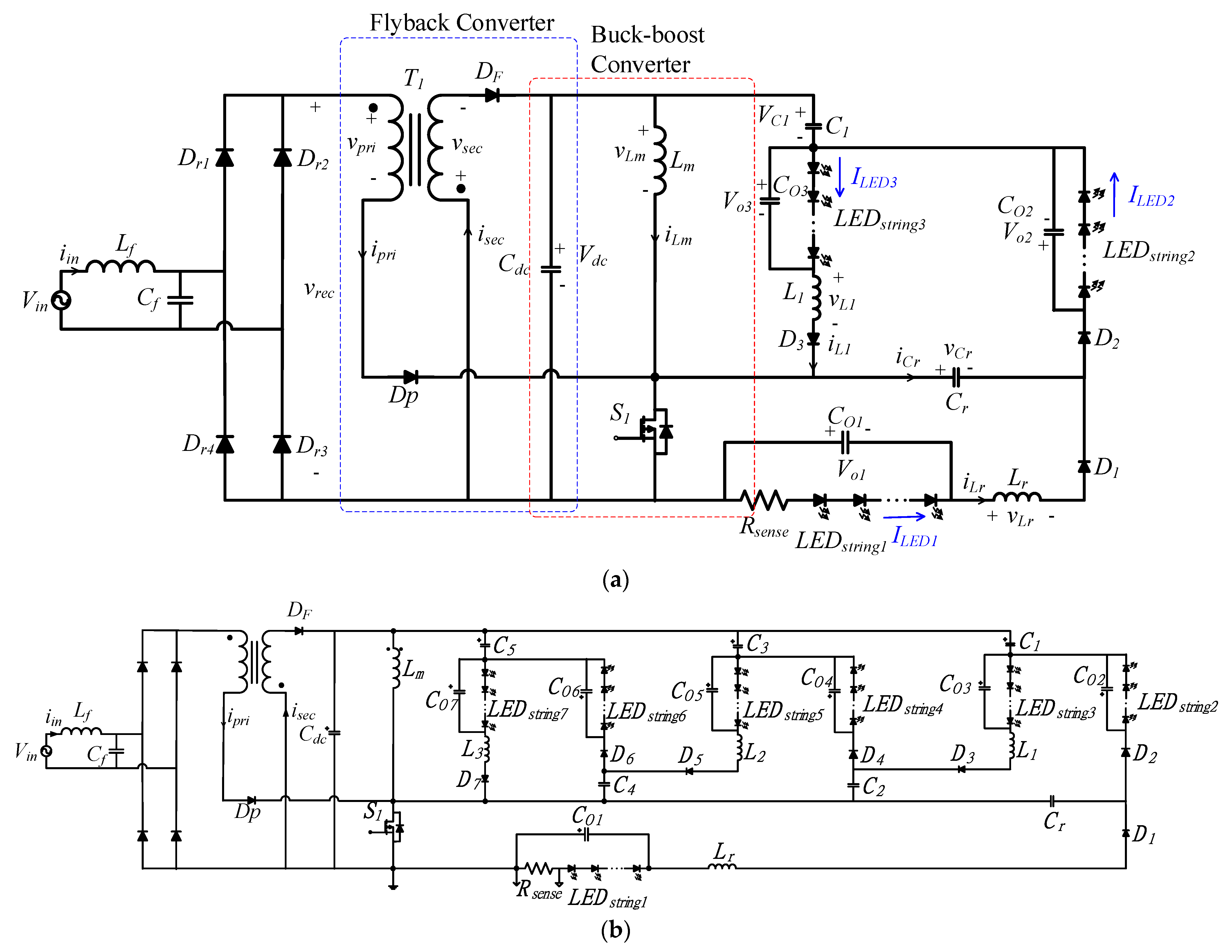
2. Circuit Configuration and Operation Mode Analysis

2.1. Circuit Configuration

Figure 1 shows the proposed single-stage high power factor LED driver. This circuit is suitable for driving odd strings of LEDs. Figure 1a,b show the LED drivers with three LED strings and seven LED strings, respectively. This article will take Figure 1a as an example to illustrate the operation principle of the proposed circuit. The circuit configuration mainly consists of a flyback converter, a buck–boost converter, and some L-C passive components used as the current balancing circuit. Both converters share an active switch S1. Vin is the mains ac voltage, Lf and Cf form a low-pass filter to remove the high-frequency current of the flyback converter. The flyback converter serves as a power-factor corrector which is designed to operate at discontinuous-current mode (DCM) to achieve high power factor and low THDi. The buck–boost converter is pulse-width modulated to adjust the power of the LED strings. By using the principle of ampere-second balance of capacitor, the current of each LED string can be equalized. The resistor Rsense is used to detect the current of the LED string one, so as long as the current of the LED string one is controlled, the current of each string of LEDs can be controlled.

2.2. Operation Mode Analysis

In order to perform the PFC function, the flyback converter is operated at DCM. In addition, the following assumptions are made to simplify circuit analysis.
  • All components are ideal.
  • The capacitors Cdc, C1, Co1, Co2, and Co3 are large enough, and the voltages across these capacitors (Vdc, VC1, Vo1, Vo2, and Vo3) can all be regarded as constant values.
  • The input voltage is an ideal sinewave, vin(t) = Vmsin(ωt), where Vm represents the amplitude of the input voltage, and ω = 2πfL represents the angular frequency.
  • The switching frequency fs of the active switch is much higher than the input voltage frequency fL (fs >> fL).
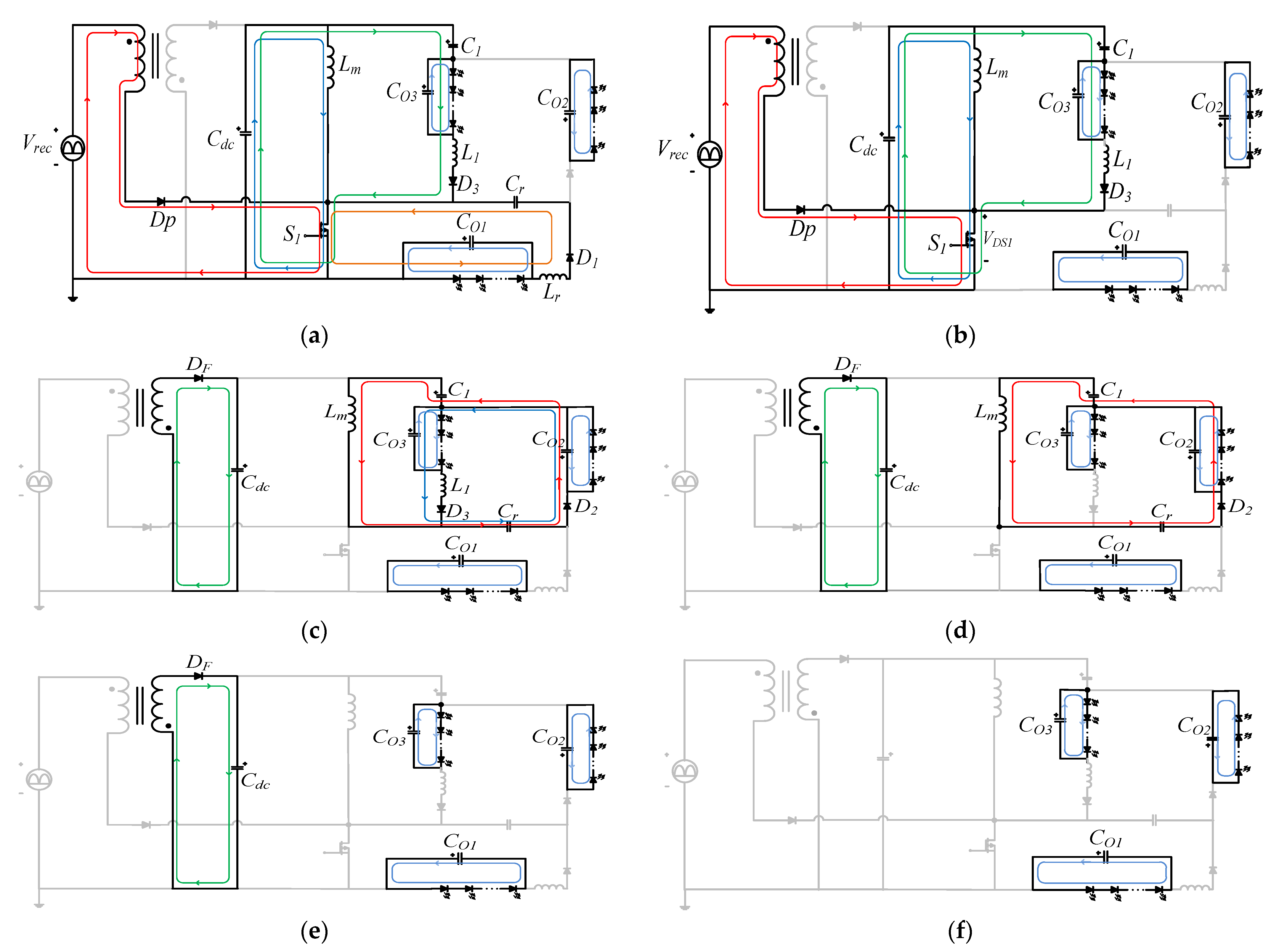
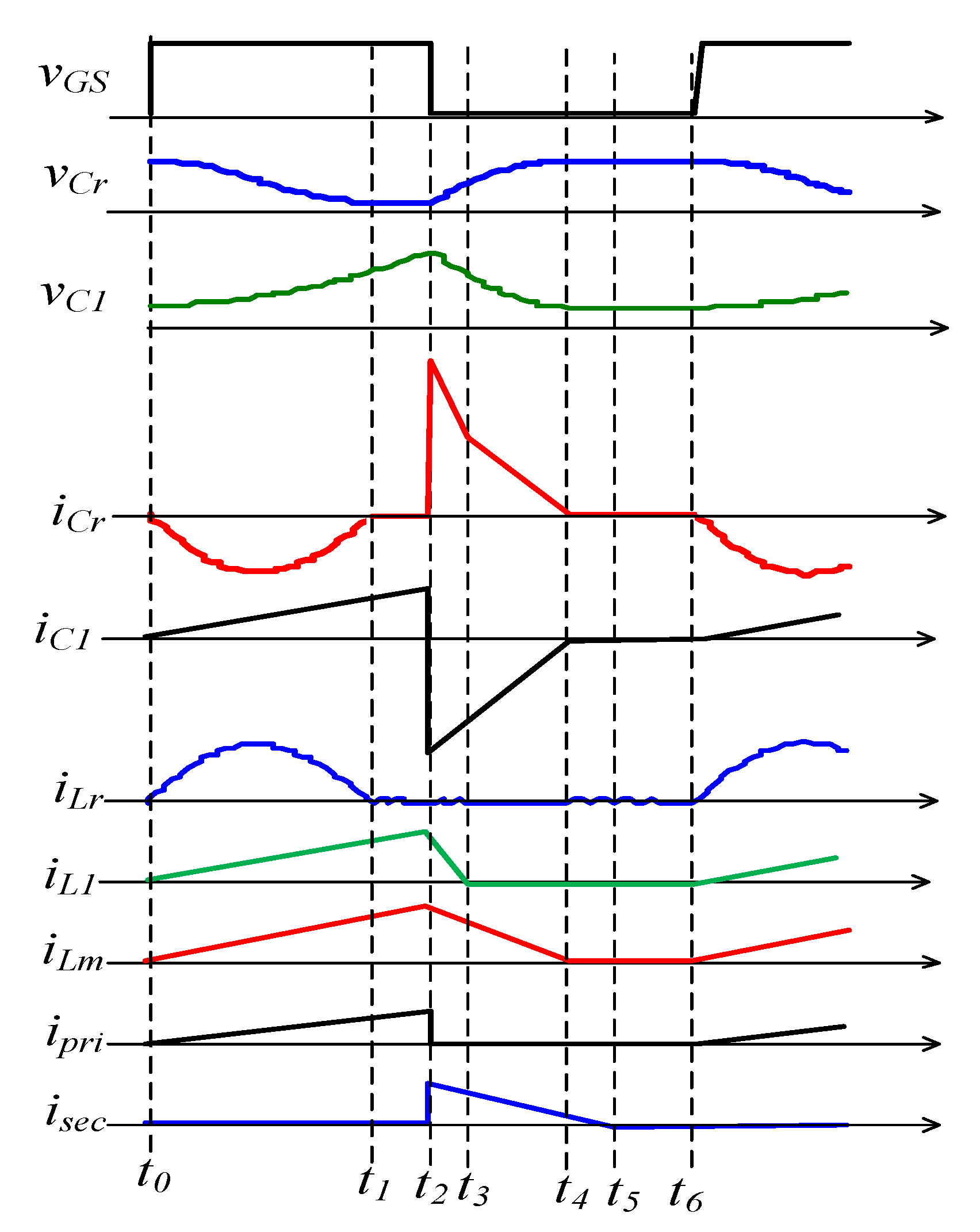
All the inductors are designed to operate at DCM. At steady-state, the circuit operation can be divided into six operation modes in a high-frequency switching cycle. Figure 2 shows the current paths of each mode where vrec represents the rectified input voltage. Figure 3 shows the conceptual voltage and current waveforms of the key components. The detailed analysis of each mode is described as follows:

2.2.1. Operation Mode I ( t 0 < t < t 1 )

The operation mode I starts at time t0 when the gate signal vGS1 changes from low-level to high-level, and S1 is turned on. The rectified voltage vrec is across on the primary winding of the transformer T1, and the primary current ipri rises linearly from zero.
i p r i ( t ) = V m | s i n ( 2 π f L t ) | L p ( t t 0 )
where Lp represents the inductance of the primary winding. At the same time, the voltage across the inductor Lm is equal to the dc-link voltage Vdc. Lm is charged and its current iLm rises linearly from zero.
i L m ( t ) = V d c L m ( t t 0 )
The voltage across the inductor L1 is equal to:
v L 1 ( t ) = V d c V C 1 V o 3
Therefore, the current iL1 starts to rise linearly from zero.
i L 1 ( t ) = V d c V C 1 V o 3 L 1 ( t t 0 )
As shown in Figure 2a, C1 is charged and its voltage rises during this mode. On the other hand, because S1 and D1 are conducting, the inductor Lr and the capacitor Cr form a resonant circuit. The voltage across Lr is equal to:
v L r ( t ) = v C r ( t ) V o 1
Its state equations can be expressed as:
{ L r d i L r ( t ) d t = v C r ( t ) V o 1 i L r ( t ) = i C r ( t ) i C r ( t ) = C r d v C r ( t ) d t
From Equation (6), the voltage across the capacitor Cr and resonant current iLr can be obtained and expressed as follows:
{ v C r ( t ) = V o 1 + [ v C r ( t 0 ) V o 1 ] c o s ω r ( t t 0 ) i L r ( t ) = v C r ( t 0 ) V o 1 Z r s i n ω r ( t t 0 )
where Zr and ωr represent the equivalent impedance and angular frequency of the resonant circuit, respectively.
{ Z r = L r / C r ω r = 2 π f r = 1 L r C r
The resonant frequency fr is designed to be greater than the switching frequency fs, and the duty ratio of S1 is designed to be large enough so that iLr would resonant to zero before S1 was turned off. When iLr resonates to zero at time t1, the circuit enters the next operation mode.

2.2.2. Operation Mode II ( t 1 < t < t 2 )

In this mode, D1 and D2 are off due to reverse bias. Currents iCr and iLr are both zero, and the voltage across Cr remains unchanged. S1 remains on, so ipri, iLm and iL1 continue to rise. When the gate signal vGS1 changes from high-level to low-level, S1 is turned off, and the circuit enters the operation mode III.

2.2.3. Operation Mode III ( t 2 < t < t 3 )

At the end of mode II, ipri, iLm and iL1 reach peak values, which are represented by ipri,peak, iLm,peak and iL1,peak, respectively. When S1 is off, there must be current loops to maintain the flux balance of T1, Lm and L1. Therefore, there is an induced current in the secondary winding of T1. The induced current isec charges the dc-link capacitor Cdc, and can be expressed as:
i s e c ( t ) = n i p r i , p e a k ( t ) V d c L s ( t t 2 )
where Ls represents the inductance of the secondary winding, and n represents the ratio of the number of turns between the primary winding and the secondary winding (n = N1/N2). In this mode, C1 is discharged and its voltage decreases. Meanwhile, the current of inductor L1 flows through L1-D3-Cr-D2-Co2-Co3, iL1 can be expressed as:
i L 1 ( t ) = i L 1 , p e a k v C r ( t ) + V o 2 + V o 3 L 1 ( t t 2 )
As shown in Figure 2c, iL1 charges Cr, Co2, and Co3. Because the peak value of isec is proportional to the input voltage, the time required for isec to decrease to zero is also proportional to the input voltage and is not a fixed value. Figure 3 shows the conceptual voltage and current waveforms when the input voltage is at the peak value. In this case, the time required for isec to drop to zero is longer than iLm and iL1. In other words, iLm and iL1 fall to zero earlier than isec. When iL1 drops to zero, the circuit enters the operation mode IV.

2.2.4. Operation Mode IV ( t 3 < t < t 4 )

In this mode, S1, D1, and D3 are off, D2 is on, the inductors Ls and Lm continue to release energy, and isec and iLm continue to decrease. At time t4, iLm drops to zero and this mode ends.

2.2.5. Operation Mode V ( t 4 < t < t 5 )

In this mode, isec continues to charge the dc-link capacitor. When isec drops to zero, the circuit enters the next operation mode.

2.2.6. Operation Mode VI ( t 5 < t < t 6 )

The currents of all inductors are equal to zero, and the LEDs are continuously lit by the energy provided by the parallel capacitors (Co1, Co2, and Co3). When the gate signal vGS1 becomes high-level, S1 is turned on again, and the circuit enters the operation mode I of the next high-frequency cycle.

3. Analysis on Current Balance and Power Factor Correction

3.1. Principle of Current Balance

According to the description of the operating mode, the discharging current of Cr flows through D1 in mode I. Therefore, the average value of this discharge current in a high-frequency cycle is equal to the average current of the LED string one. In mode III and mode IV, Cr is charged. As shown in and Figure 2c,d, this charging current flows through D2, so its average value is equal to the average current of the LED string two. Based on the principle of the ampere-second balance of the capacitor, that is that the net current of a capacitor will equal zero. In other words, the average value of the capacitor charging current is equal to the average value of its discharge current. Therefore, the average current of LED string one and LED string two would be equal.
I L E D 1 = I L E D 2
In mode I and mode II, C1 is charged through D3. Similarly, the average value of the charging current of C1 is equal to the average current of the LED string three. In mode III and mode IV, C1 is charged through D2, and the average value of the discharging current of C1 will be equal to the average current of the LED string two. Applying the ampere-second balance principle to C1, it can be concluded that the average currents of the LED string two and the LED string three are equal.
I L E D 2 = I L E D 3
Combining Equations (11) and (12), the current flowing through each LED string is equal.
I L E D 1 = I L E D 2 = I L E D 3

3.2. Flyback PFC Circuit

The flyback converter is designed to operate at DCM during the entire input voltage cycle. The primary current ipri of T1 rises linearly from zero during mode I and mode II (t0-t2), and rises to a peak value, which can be expressed as:
i p r i , p e a k ( t ) = V m D T s sin ( 2 π f L t ) L p
where D represents the duty ratio of the active switch. High-power factor and low THDi can be achieved by operating the flyback converter at DCM [20]. The high-frequency components of ipri can be filtered out by using the low-pass filter (Lf, Cf), so that the input current iin will be equal to the average value of ipri in each high-frequency cycle.
The input power is equal to the average value of the instantaneous power, which can be expressed as:
P i n = 1 2 π 0 2 π V m sin ( 2 π f L t ) · i i n ( t ) d ( 2 π f L t ) = V m 2 4 L P D 2 T S
Assuming that the conversion efficiency of the circuit is η, the output power is equal to:
P O = P L E D = η × P i n = η V m 2 D 2 T S 4 L P

4. Design Equations of Circuit Parameters

4.1. Design Equations of the Flyback Converter

From Equation (16), the primary inductance Lp of T1 can be obtained, which is expressed by the following equation:
L P = η V m 2 D 2 T s 4 P o
The transformer primary current ipri rapidly drops to zero at the moment when the active switch is turned off. In order to maintain the magnetic flux balance of T1, it will induce a current in the secondary winding. The secondary current isec can be obtained by substituting Equation (14) into Equation (9). At t2, isec starts to decrease linearly from a peak value, and reaches zero at t5. The fall time of isec is denoted as Toff.
T o f f = t 5 t 2
The primary inductance and secondary inductance of T1 is proportional to the square of the number of turns, that is:
L s = ( n 2 n 1 ) 2 L p = ( 1 n ) 2 L p
Combining Equations (9), (14), (18) and (19) gets:
T o f f ( t ) = V m | sin ( 2 π f L t ) | n V d c D T s
At DCM operation, Toff is less than (1-D)Ts.
T o f f ( t ) = V m | sin ( 2 π f L t ) | n V d c D T s < ( 1 D ) T s
The longest fall time Toff,max occurs when the input voltage is at its maximum and is equal to:
T o f f , m a x = V m D T s n V d c
In order to operate the flyback converter at DCM during the entire line cycle, the following inequality must exist:
V d c V m > 1 n · D 1 D
The higher the amplitude of the input voltage, the higher the dc-link voltage required to satisfy the inequality (23). However, since the active switch is not operated at zero-voltage switching on (ZVS), high dc-link voltage will cause more switching losses. It means that the proposed circuit is not valid for a universal input voltage range (110–220 Vrms). When the input voltage is different, the turn ratio of the coupled inductor of the flyback converter should also be different. In this way, an adequate dc-link voltage can be chosen to satisfy the inequality (23).

4.2. Design Equations of the Current Balancing Circuit

As shown in Figure 3, both inductors Lm and L1 are operated at DCM. At steady-state operation, the average value of the inductor currents is zero. Therefore, the increase in iL1 when S1 is on is the same as the decrease when S1 is off.
( V d c V C 1 V O 3 ) D T s L 1 + ( V O 3 V O 2 V C r ) D o f f , L 1 T s L 1 = 0
where Doff,L1 is defined as the ratio of the falling time of iL1 to Ts. Generally, the voltage and current of each LED string are approximately equal, that is VO1 = VO2 = VO3 = VO, and ILED1 = ILED2 = ILED3 = ILED from Equation (24), which gets:
D o f f , L 1 = ( V d c V C 1 V O ) D T s 2 V O + V C r
The net change of iLm when S1 is turned on and off is also equal to zero.
V d c D T s L m + ( V C 1 V O 2 V C r ) D o f f , L m T s L m = 0
where Doff,Lm is defined as the ratio of the falling time of iLm to Ts, and is equal to:
D o f f , L m = D V d c V O + V C r V C 1
As shown in Figure 1, ILED3 will be equal to the average current of L1 since the net current of C1 is zero.
I L E D 3 = 1 2 ( V d c V C 1 V O 3 ) D ( D + D o f f , L 1 ) T s L 1
Substituting Equation (25) into Equation (28), the inductance L1 can be obtained, which is expressed as follows:
L 1 = 1 2 ( V d c V C 1 V O 3 ) D T s I L E D 3 · ( D + ( V d c V C 1 V O ) D 2 V O + V C r )
During mode III and mode IV, iLM and iL1 flow through D2, therefore, ILED2 can be expressed as:
I L E D 2 = 1 2 ( V d c D D o f f , L m T s L m + ( V d c V C 1 V O 3 ) D D o f f , L 1 T s L 1 )
Substituting Equations (25), (27) and (29) into Equation (30), the inductance Lm can be obtained, which is expressed as follows:
L m = V d c 2 D 2 T s ( V d c V C 1 + V C r + V O ) 2 I L E D ( 2 V O + V C r ) ( V O + V C r V C 1 )
As stated in mode I, iLr resonances to zero before S1 being turned off. Therefore, the following inequality must exist:
π L r C r < D T s
The inductance Lr can be obtained from Equation (32), which is expressed as follows:
L r < D 2 T s 2 C r π 2 = D 2 C r π 2 f s 2

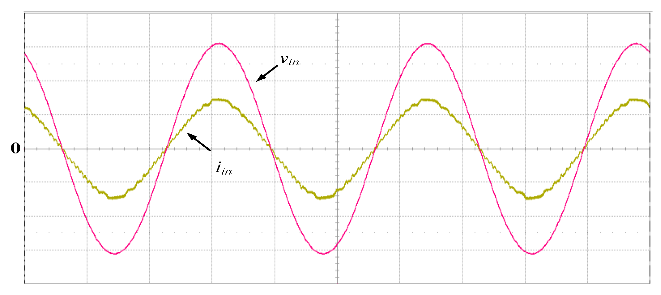
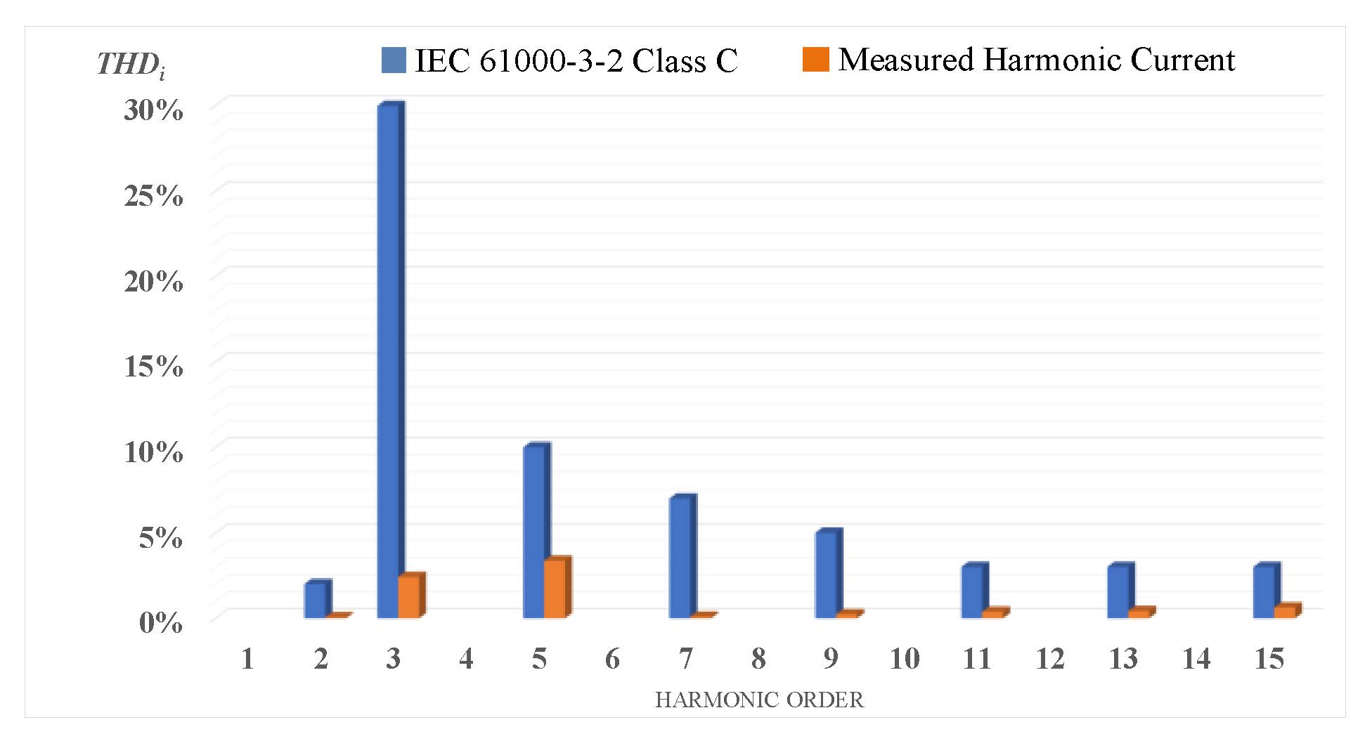
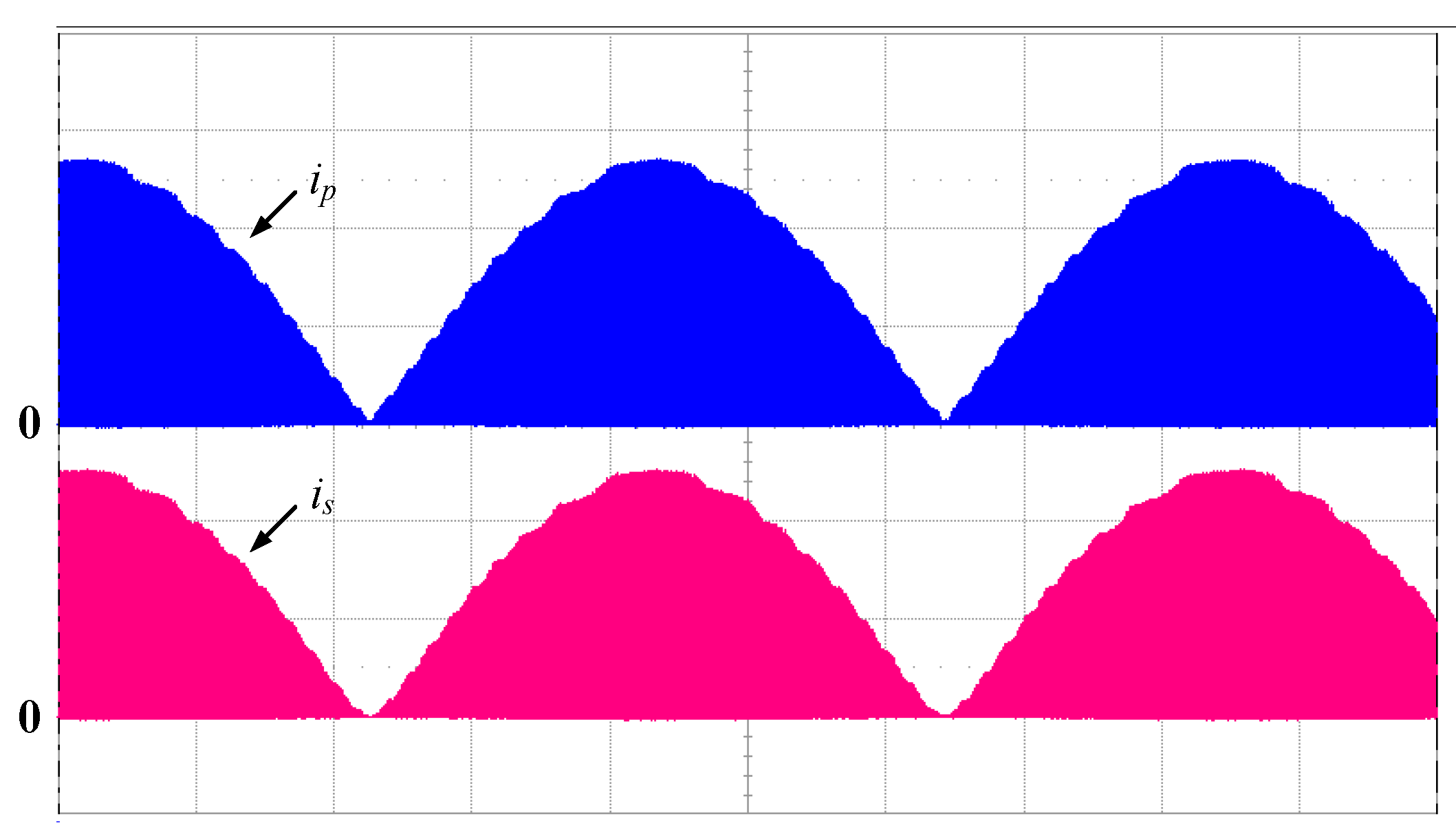
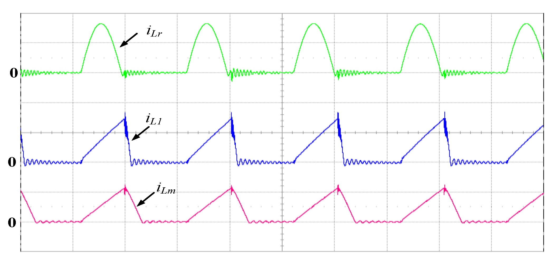
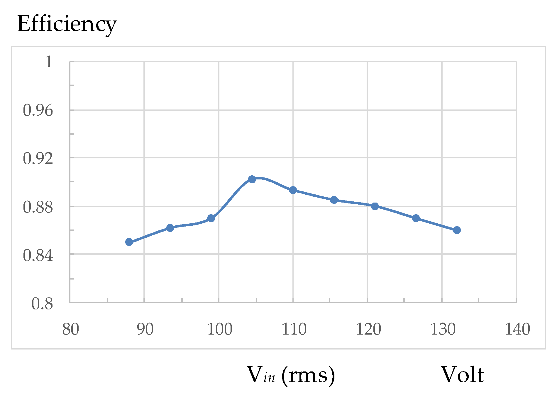
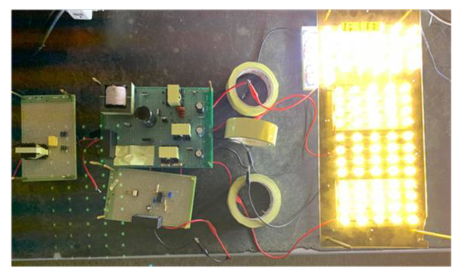
5. Experimental Results

A 90-W prototype circuit was built and tested to demonstrate the functions of power factor correction and current balancing capability. Table 1 shows the specification of the proposed LED driver. The load is three LED strings. Each string consists of 30 1-W LEDs connected in series. The rated voltage and current of each LED is 3.05 V and 0.328 A, respectively. Table 2 shows the circuit parameters. Some of the circuit parameters are designed as follows:

5.1. Component Parameters Design

5.1.1. Primary and Secondary Inductances of Transformer T1

The turns ratio n of T1 is chosen as one. Assuming that the overall efficiency of the circuit is 90% and using Equation (17), the primary inductance and the secondary inductance can be calculated.
L p = L s = η V m 2 D 2 T s 4 P o = 0.95 × 156 2 × 0.4 2 4 × 90 × 50 × 10 3 = 194.7   μ H

5.1.2. Inductance and Capacitance of the Resonant Circuit

The capacitance of the resonant circuit can be obtained as follows:
C r = 1 2 f s R L E D = 1 2 × 50 × 10 3 × 279 = 35.8   nF
In order to meet Equation (33), inductance of the resonant circuit must satisfy the following inequality:
L r < D 2 C r π 2 f s 2 = 0.4 2 35.8 × 10 9 × π 2 × ( 50 × 10 3 ) 2 = 181   μ H
Here, Lr is chosen to be 170 μH.

5.1.3. Inductances of L1 and Lm

Using Equation (23), the minimum value of the dc-link capacitance can be obtained.
V d c > 1 n · D 1 D · V m = 0.4 × 156 1 × 0.6 = 104   V
Here Vdc is chosen to be 110 V.
The average voltage of the resonant capacitor is approximately equal to half of its maximum voltage. Therefore, the average voltage of the resonant capacitor is equal to:
V C r = 1 2 2 I L E D 2 R L E D C r f s = 1 2 2 × 0.328 2 × 279 35.8 × 10 9 × 50 × 10 3 = 91.56   V
The inductance L1 can be calculated by using Equation (29).
L 1 = 1 2 ( V d c V C 1 V O 3 ) D T s I L E D 3 · ( D + ( V d c V C 1 V O ) D 2 V O + V C r ) = 278.3   μ F
The inductance Lm can be calculated by using Equation (31).
L m = V d c 2 D 2 T s ( V d c V C 1 + V C r + V O ) 2 I L E D ( 2 V O + V C r ) ( V O + V C r V C 1 ) = 325.87   μ F

5.2. Control Circuit and Experimental Results

The closed-loop control circuit of the driving circuit adopts the PWM controller (TL494), as shown in Figure 4. The output of TL494 is used to turn the active switch on and off, and its frequency can be determined by capacitor CT and resistor RT. The voltage across Rsense in the main circuit is sensed via R1 and R2 and compared with the internal sawtooth-wave voltage of TL494 to adjust the duty ratio of the active switch. In this way, the LED current can be regulated.
Figure 5, Figure 6, Figure 7, Figure 8 and Figure 9 show the experimental waveforms when the circuit is operating at rated power (90 W). The input voltage and current waveforms are shown in Figure 5. It is demonstrated that the input current is an approximate sinusoidal wave and in phase with the input voltage. It ensures high power factor and low THDi. The measured power factor and THDi are 0.99 and 2.91%, respectively. The measured output power and total losses are 90.3 W and 10.8 W, respectively. The circuit efficiency is calculated to be 89.3%. Figure 6 shows the harmonic spectrum of the input line current. The THDi is 2.91% and all harmonics are in compliance with the IEC 61000-3-2 Class C. Figure 7 shows the waveforms of the primary and secondary currents of T1. Both currents are operated at DCM, which is consistent with the design goal. Figure 8 shows the current waveforms of the inductors Lm, L1, and Lr, showing that iLr has resonated to zero before the active switch is turned off; iL1 drops to zero before iLm, and they all operate at DCM. Figure 9 shows the current waveforms of three LED strings with the same number of LEDs, showing that the current of each string is equal. This proves the current balancing capability of the circuit.
In order to further verify the current balancing function, the circuit driving three LED strings of different numbers of LEDs was tested. The number of LEDs in the three strings are 33, 30, and 27, respectively. Figure 10 shows measured currents of the three LED strings. It was demonstrated that the current of each string still remains the same when the load power changes by plus or minus 10%.
When the input voltage changes within a range of +/−20%, the duty cycle needs to be adjusted to maintain rated power operation. Figure 11 shows the measured efficiency at different input voltages. The circuit efficiency only slightly changes under different voltages. The LED power can be regulated by the control scheme of PWM. Figure 12 shows the currents of each string at 75%, 50% and 25% rated power. Similarly, when operating at different powers, the current of each string of LEDs is still the same. Figure 13 shows the measured efficiency at different output power. As shown, the circuit efficiency drops to 73.5% at 25% rated power. Figure 14 shows the prototype LED driver.

6. Conclusions

A single-stage LED drive circuit with power factor correction and current balancing capability is proposed. The circuit configuration mainly integrated a flyback converter, a buck–boost converter and a current balancing circuit. The flyback converter was used as a PFC converter, and the winding current was designed to operate at DCM to effectively reduce the THDi and improve the power factor; while the current balancing circuit applied the principle of capacitor ampere-second balance to achieve the same current for each LED string. Only one active switch was used and controlled by the method of PWM. A 90-W prototype circuit was built and tested. At rated power operation, the measured power factor was 0.99, the THDi was 2.91%, and the conversion efficiency was 89.3%. In addition, even where the number of LEDs in each string was different, the current balancing capability could still be achieved. Finally, the LED power was regulated from 100% to 25% rated power. The satisfactory experimental results have proved the feasibility of the proposed LED driver.

Author Contributions

Y.-H.Y. and H.-L.C. conceived and designed the circuit; C.-A.C. and Y.-N.C. performed circuit simulations and designed parameters of the circuit components; Z.-X.W. carried out the prototype converter, and measured as well as analyzed experimental results; H.-L.C. wrote the paper and Y.-H.Y. revised it for submission. All authors have read and agreed to the published version of the manuscript.

Funding

This research received no external funding.

Acknowledgments

This work was supported by the Ministry of Science and Technology, R.O.C. under Grant MOST 108-2221-E-214-01.

Conflicts of Interest

The authors declare no conflict of interest.

References

  1. Moon, S.C.; Koo, G.B.; Moon, G.W. Dimming-feedback control method for TRIAC dimmable LED drivers. IEEE Trans. Ind. Electron. 2015, 62, 960–965. [Google Scholar] [CrossRef]
  2. Lee, E.S.; Choi, B.H.; Nguyen, D.T.; Jang, G.C.; Rim, C.T. Versatile LED drivers for various electronic ballasts by variable switched capacitor. IEEE Trans. Power Electron. 2016, 31, 1489–1502. [Google Scholar] [CrossRef]
  3. Alonso, J.M.; Gacio, D.; Calleja, A.J.; Ribas, J.; Corominas, E.L. A study on led retrofit solutions for low-voltage halogen cycle lamps. IEEE Trans. Ind. Appl. 2012, 48, 1673–1682. [Google Scholar] [CrossRef]
  4. Liu, X.; Zhou, Q.; Xu, J.; Lei, Y.; Wang, P.; Zhu, Y. High-efficiency resonant LED backlight driver with passive current balancing and dimming. IEEE Trans. Ind. Electron. 2018, 65, 5476–5486. [Google Scholar] [CrossRef]
  5. Zhao, C.; Xie, X.; Liu, S. Multioutput LED drivers with precise passive current balancing. IEEE Trans. Power Electron. 2013, 28, 1438–1448. [Google Scholar] [CrossRef]
  6. Li, S.N.; Zhong, W.X.; Chen, W.; Hui, S.Y.R. Novel self-configurable current-mirror techniques for reducing current imbalance in parallel light-emitting diode (LED) strings. IEEE Trans. Power Electron. 2012, 27, 2153–2162. [Google Scholar] [CrossRef] [Green Version]
  7. Li, S.; Hui, S.Y.R. Self-configurable current-mirror circuit with short-circuit and open-circuit fault tolerance for balancing parallel light-emitting diode (LED) string current. IEEE Trans. Power Electron. 2014, 29, 5498–5550. [Google Scholar] [CrossRef]
  8. Qu, X.; Wong, S.C.; Tse, C.K. Noncascading structure for electronic ballast design for multiple LED lamps with independent brightness control. IEEE Trans. Power Electron. 2010, 25, 331–340. [Google Scholar]
  9. Hu, U.; Jovanovic, M.M. LED driver with self-adaptive drive voltage. IEEE Trans. Power Electron. 2008, 23, 3116–3125. [Google Scholar] [CrossRef]
  10. Chen, H.; Zhang, Y.; Ma, D. A SIMO parallel-string driver IC for dimmable LED backlighting with local bus voltage optimization and single time-shared regulation loop. IEEE Trans. Power Electron. 2012, 27, 452–462. [Google Scholar] [CrossRef]
  11. Yang, W.H.; Yang, H.A.; Huang, C.J.; Chen, K.H. A high-efficiency single-inductor multiple-output buck-type LED driver with average current correction technique. IEEE Trans. Power Electron. 2018, 33, 3375–3385. [Google Scholar] [CrossRef]
  12. Qu, X.; Wong, S.C.; Tse, C.K. An improved LCLC current-source-output multistring LED driver with capacitive current balancing. IEEE Trans. Power Electron. 2015, 30, 5783–5791. [Google Scholar] [CrossRef]
  13. Wu, X.; Zhang, J.; Qian, Z. Analysis and design considerations of LLCC resonant multioutput DC/DC LED driver with charge balancing and exchanging of secondary series resonant capacitors. IEEE Trans. Power Electron. 2015, 30, 780–789. [Google Scholar] [CrossRef]
  14. Choi, S.; Kim, T. Symmetric current balancing circuit for LED backlight with dimming. IEEE Trans. Ind. Electron. 2012, 59, 1698–1707. [Google Scholar] [CrossRef]
  15. Zhang, J.; Wang, J.; Wu, X. A capacitor-isolated LED driver with inherent current balance capability. IEEE Trans. Ind. Electron. 2012, 59, 1708–1716. [Google Scholar] [CrossRef]
  16. Alonso, J.M.; Viña, J.; Vaquero, D.G.; Martínez, G.; Osório, R. Analysis and design of the integrated double buck-boost converter as a high-power-factor driver for power-LED lamps. IEEE Trans. Ind. Electron. 2012, 59, 1689–1697. [Google Scholar] [CrossRef]
  17. Li, Y.C.; Chen, C.L. A novel primary-side regulation scheme for single-stage high-power-factor AC–DC LED driving circuit. IEEE Trans. Ind. Electron. 2013, 60, 4978–4986. [Google Scholar] [CrossRef]
  18. Wang, Y.; Guan, Y.; Ren, K.; Wang, W.; Xu, D. A single-stage LED driver based on BCM boost circuit and LLC converter for street lighting system. IEEE Trans. Ind. Electron. 2015, 62, 5446–5457. [Google Scholar] [CrossRef]
  19. Cheng, C.A.; Cheng, H.L.; Chung, T.Y. A novel single-stage high-power-factor LED street-lighting driver with coupled inductors. IEEE Trans. Ind. Appl. 2014, 50, 2821–2826. [Google Scholar] [CrossRef]
  20. Erickson, R.; Madigan, M.; Singer, S. Design of a simple high-power-factor rectifier based on the flyback converter. In Proceedings of the IEEE Applied Power Electronics Conference and Exposition, Los Angeles, CA, USA, 11 March 1990; pp. 792–801. [Google Scholar] [CrossRef]
Figure 1. Proposed single-stage single-switch LED drivers (a) three LED strings; (b) seven LED strings.
Electronics 10 01340 g001
Figure 2. Operation modes (a) mode I; (b) mode II; (c) mode III; (d) mode IV; (e) mode V; (f) mode VI.
Electronics 10 01340 g002
Figure 3. Conceptual voltage and current waveforms.
Electronics 10 01340 g003
Figure 4. Closed-loop control circuit.
Electronics 10 01340 g004
Figure 5. Input voltage and current waveforms. (vin: 100 V/div, iin: 1.0 A/div, time: 5 ms/div).
Electronics 10 01340 g005
Figure 6. Harmonic spectrum of the input line current.
Electronics 10 01340 g006
Figure 7. Primary and secondary currents of T1. (ip: 2 A/div, is: 2 A/div, time: 2 ms/div).
Electronics 10 01340 g007
Figure 8. Current waveforms of iLr, iL1 and iLm. (iLr: 1 A/div, iLm: 2 A/div, iL1: 1 A/div, time: 10 µs/div).
Electronics 10 01340 g008
Figure 9. Waveforms of ILED1, ILED2 and ILED3 with equal number of LEDs. (ILED1: 200 mA/div, ILED2: 200 mA/div, ILED3: 200 mA/div, time: 5 ms/div).
Electronics 10 01340 g009
Figure 10. Waveforms of ILED1, ILED2 and ILED3 with different numbers of LEDs. (ILED1: 200 mA/div, ILED2: 200 mA/div, ILED3: 200 mA/div, time: 5 ms/div).
Electronics 10 01340 g010
Figure 11. Measured circuit efficiency at different input voltages.
Electronics 10 01340 g011
Figure 12. LED currents at different power levels: (a) 75% rated power, (b) 50% rated power and (c) 25% rated power.
Electronics 10 01340 g012
Figure 13. Measured circuit efficiency at different output power levels.
Electronics 10 01340 g013
Figure 14. 90-W LED prototype circuit.
Electronics 10 01340 g014
Table 1. Specification of the proposed LED driver.
Input voltage vin110 V ± 10% (rms), 60 Hz
Output power Po90 W (30 W × 3)
LED voltage VLED91.5 V (3.05 V × 30)
LED voltage ILED0.328 A
Equivalent LED Resistance RLED279 Ω
Switching frequency fs50 kHz
Duty ratio D0.4
Table 2. Circuit parameters.
The low-pass inductance Lf 1.89 mH
The low-pass capacitance Cf0.47 μF
Dc-link capacitance Cdc330 μF
Output capacitance Co1~Co347 μF
Capacitance C110 μF
Capacitance Cr35.2 μF
Inductance Lp, Ls194.7 µH
Inductances Lm, L1, Lr326 µH, 278 µH, 170 µH
Active switches S1SPW47N60C3
Bridge-rectifier diodes Dr1~Dr4MUR460
Diodes Dp, D, Db, D1~D3C3D10060 A
Publisher’s Note: MDPI stays neutral with regard to jurisdictional claims in published maps and institutional affiliations.

