
Metal-Insulator-Metal Waveguide-Based Racetrack Integrated Circular Cavity for Refractive Index Sensing Application

 ,
,  ,
,  and
and 
Abstract
:1. Introduction
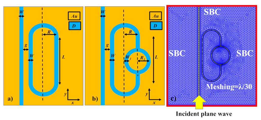
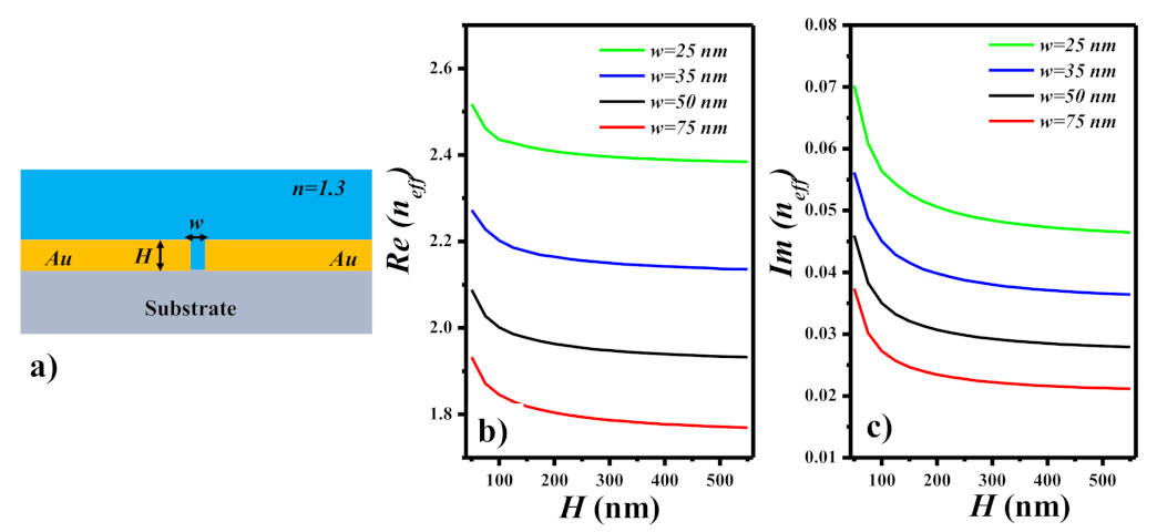
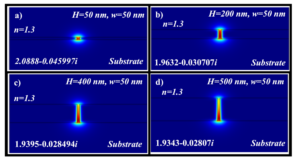
2. Device Design
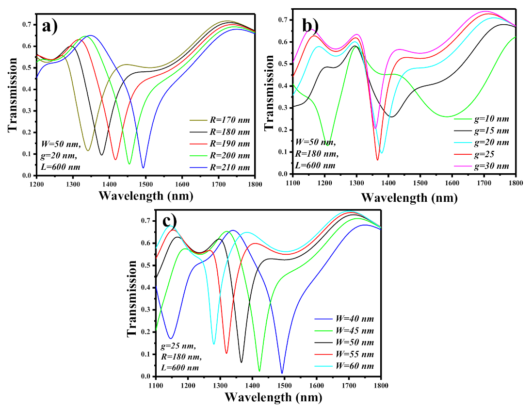
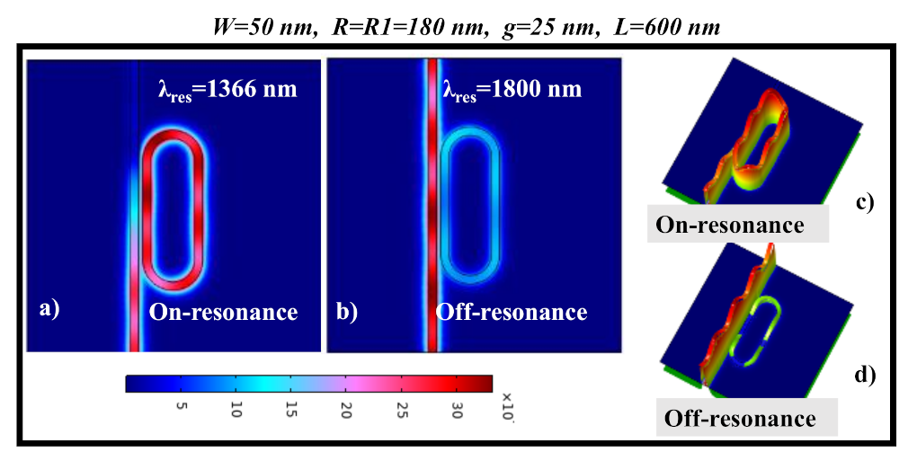
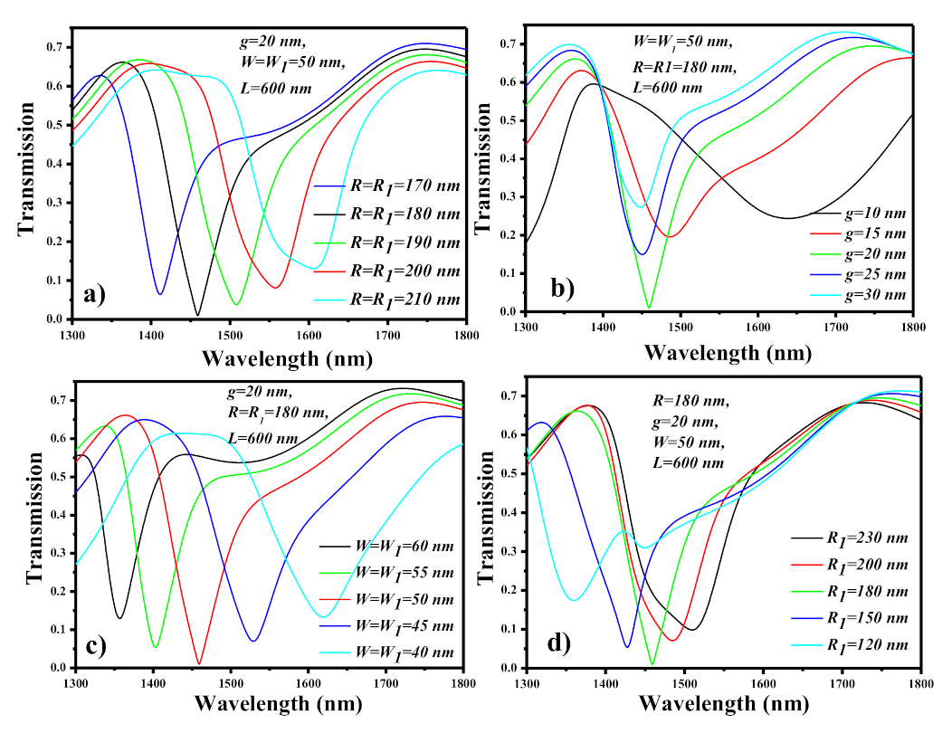
3. SRTC Configuration
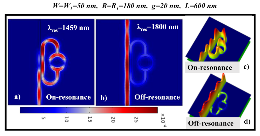
4. RTICC Configuration
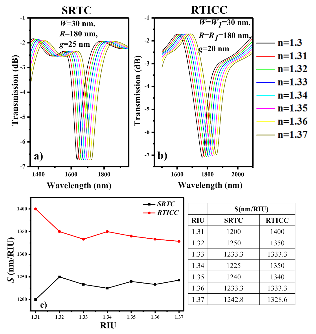
5. Findings and Analysis
6. Conclusions
Author Contributions
Funding
Acknowledgments
Conflicts of Interest
Abbreviations
| Standard racetrack cavity | SRTC |
| Racetrack integrated circular cavity | RTICC |
| Metal-insulator-metal | MIM |
| Waveguide | WG |
| Refractive index | RI |
| Effective refractive index | neff |
| Finite element method | FEM |
| Sensitivity | S |
| Figure of merit | FOM |
References
- Anwar, R.S.; Ning, H.; Mao, L. Recent advancements in surface plasmon polaritons-plasmonics in subwavelength structures in microwave and terahertz regimes. Digit. Commun. Netw. 2018, 4, 244–257. [Google Scholar] [CrossRef]
- Zhang, J.; Zhang, L.; Xu, W. Surface plasmon polaritons: Physics and applications. J. Phys. D Appl. Phys. 2012, 45, 113001. [Google Scholar] [CrossRef]
- Zhang, T.; Shan, F. Development and application of surface plasmon polaritons on optical amplification. Plasmon. Nanophotonics 2014, 2014, 495381. [Google Scholar] [CrossRef]
- Karabchevsky, A.; Katiyi, A.; Ang, A.S.; Hazan, A. On-chip nanophotonics and future challenges. Nanophotonics 2020, 9, 3733–3753. [Google Scholar] [CrossRef]
- Zhang, M.; Wang, Z. Analytical method for metal-insulator-metal surface plasmon polaritons waveguide networks. Opt. Express 2019, 27, 303–321. [Google Scholar] [CrossRef]
- Niu, L.; Xiang, Y.; Cai, W.; Zhao, X.; Zhang, N.; Qi, J.; Zhang, X.; Xu, J. Plasmonic Tamm states in insulator-metal-insulator waveguides. J. Opt. Soc. Am. B 2018, 35, 1368–1373. [Google Scholar] [CrossRef]
- Chen, Z.-X.; Wu, Z.-J.; Ming, Y.; Zhang, X.-J.; Lu, Y.-Q. Hybrid plasmonic waveguide in a metal V-groove. AIP Adv. 2014, 4, 017103. [Google Scholar] [CrossRef] [Green Version]
- Feigenbaum, E.; Orenstein, M. Nano plasmon polariton modes of a wedge cross section metal waveguide. Opt. Express 2006, 14, 8779–8784. [Google Scholar] [CrossRef] [PubMed] [Green Version]
- Fevrier, M.; Gogol, P.; Aassaime, A.; Megy, R.; Delacour, C.; Chelnokov, A.; Apuzzo, A.; Blaize, S.; Lourtioz, J.-M.; Dagens, B. Gaint coupling effect between metal nanoparticle chain and optical waveguide. Nano Lett. 2012, 12, 1032–1037. [Google Scholar] [CrossRef]
- Zhai, X.; Liu, Y.; Li, H.; Wujiaihemaiti, R.; Zhu, Y.; Wang, L. Analysis of filter and waveguide effect based on the MIM nanodisk with a metallic block. J. Nanomater. 2015, 2015, 541409. [Google Scholar] [CrossRef] [Green Version]
- Wang, L.; Wang, L.-L.; Zeng, Y.-P.; Xiang, D.; Zhai, X.; Li, X.-F.; Huang, W.-Q. A triangular shaped channel MIM waveguide filter. J. Mod. Opt. 2012, 59, 1686–1689. [Google Scholar] [CrossRef]
- Butt, M.A.; Khonina, S.N.; Kazanskiy, N.L. Ultra-short lossless plasmonic power splitter design based on metal-insulator-metal waveguide. Laser Phys. 2019, 30, 016201. [Google Scholar] [CrossRef]
- Chen, F.; Xu, Y. Tunable power splitter based on MIM waveguide-rectangular cavity system with Kerr material. Mod. Phys. Lett. B 2016, 30, 1650376. [Google Scholar] [CrossRef]
- Lu, H.; Wang, G.; Liu, X. Manipulation of light in MIM plasmonic waveguide systems. Chin. Sci. Bull. 2013, 58, 3607–3616. [Google Scholar] [CrossRef] [Green Version]
- Butt, M.A.; Khonina, S.N.; Kazanskiy, N.L. A multichannel metallic dual nano-wall square split-ring resonator:design analysis and applications. Laser Phys.Lett. 2019, 16, 126201. [Google Scholar] [CrossRef]
- Butt, M.A.; Khonina, S.N.; Kazanskiy, N.L. A plasmonic colour filter and refractive index sensor applications based on metal-insulator-metal square micro-ring cavities. Laser Phys. 2020, 30, 016205. [Google Scholar] [CrossRef]
- Mahmud, R.A.; Faruque, M.O.; Sagor, R.H. A highly sensitive plasmonic refractive index sensor based on triangular resonator. Optics Communications 2021, 483, 126634. [Google Scholar] [CrossRef]
- Khonina, S.N.; Kazanskiy, N.L.; Butt, M.A.; Kazmierczak, A.; Piramidowicz, R. Plasmonic sensor based on metal-insulator-metal waveguide square ring cavity filled with functional material for the detection of CO2 gas. Opt. Express 2021, 29, 16584. [Google Scholar] [CrossRef]
- Butt, M.A. Numerical investigation of a small footprint plasmonic Bragg grating structure with a high extinction ratio. Photonics Lett. Pol. 2020, 12, 82–84. [Google Scholar] [CrossRef]
- Butt, M.A.; Kazanskiy, N.L.; Khonina, S.N. Highly integrated plasmonic sensor design for the simultaneous detection of multiple analytes. Curr. Appl. Phys. 2020, 20, 1274–1280. [Google Scholar] [CrossRef]
- Butt, M.A.; Khonina, S.N.; Kazanskiy, N.L. An array of nano-dots loaded MIM square ring resonator with enhanced sensitivity at NIR wavelength range. Optik 2020, 202, 163655. [Google Scholar] [CrossRef]
- Huang, Y.-X.; Xie, Y.-X.; Zhao, W.-L.; Che, H.-J.; Xu, W.-H.; Li, X.; Li, J.-C. A plasmonic refractive index sensor based on a MIM waveguide with a side-coupled nanodisk resonator. In Proceedings of the IEEE 20th International Conference on Embedded and Real-Time Computing Systems and Applications, Chongqing, China, 20–22 August 2014. [Google Scholar]
- Kazanskiy, N.L.; Butt, M.A. Enhancing the sensitivity of a standard plasmonic MIM square ring resonator by incorporating nanodots in the cavity. Photonics Lett. Pol. 2020, 12, 1–3. [Google Scholar]
- Kazanskiy, N.L.; Butt, M.A.; Khonina, S.N. Nanodots decorated MIM semi-ring resonator cavity for biochemical sensing applications. Photonics Nanostruct. Fundam. Appl. 2020, 42, 100836. [Google Scholar] [CrossRef]
- Kazanskiy, N.L.; Butt, M.A.; Degtyarev, S.A.; Khonina, S.N. Achievements in the development of plasmonic waveguide sensors for measuring the refractive index. Comput. Opt. 2020, 44, 295–318. [Google Scholar] [CrossRef]
- Kazanskiy, N.L.; Khonina, S.N.; Butt, M.A. Plasmonic sensors based on metal-insulator-metal waveguides for refractive index sensing applications: A brief review. Phys. E Low-Dimens. Syst. Nanostruct. 2020, 117, 113798. [Google Scholar] [CrossRef]
- Butt, M.A.; Kazanskiy, N.L. Nanoblocks embedded in L-shaped nanocavity of a plasmonic sensor for best sensor performance. Opt. Appl. 2021, 51, 109–120. [Google Scholar]
- Chen, J.; Li, J.; Liu, X.; Rohimah, S.; Tian, H.; Qi, D. Fano resonance in a MIM waveguide with double symmetric rectangular stubs and its sensing characteristics. Opt. Commun. 2021, 482, 126563. [Google Scholar] [CrossRef]
- Yan, S.; Yang, X.; Xu, D.; Su, H.; Wu, X.; Hua, E. MIM structure with inverted M-type cavity for sensing applications. IEEE Sens. J. 2021, 21, 7468. [Google Scholar] [CrossRef]
- Butt, M.A.; Khonina, S.N.; Kazanskiy, N.L. Metal-insulator-metal nano square ring resonator for gas sensing applications. Waves Random Complex Media 2021, 31, 146–156. [Google Scholar] [CrossRef]
- He, Q.; Huo, Y.; Guo, Y.; Niu, Q.; Hao, X.; Cui, P.; Wang, Y.; Song, M. Multiple adjustable Fano resonance based on double half ring resonator and its application. Phys. Scr. 2021, 96, 065504. [Google Scholar] [CrossRef]
- Rahmatiyar, M.; Afsahi, M.; Danaie, M. Design of a refractive index plasmonic sensor based on a ring resonator coupled to a MIM waveguide containing tapered defects. Plasmonics 2020, 15, 2169–2176. [Google Scholar] [CrossRef]
- Jumat, S.Z.B.H.; Chao, C.-T.C.; Chau, Y.F.C.; Mahadi, A.H.; Kooh, M.R.R.; Kumara, N.T.R.N.; Chiang, H.-P. Plasmonic refractive index sensor based on the combination of rectangular and circular resonators including baffles. Chin. J. Phys. 2021, 71, 286–299. [Google Scholar] [CrossRef]
- Rakhshani, M.R. Refractive index sensor based on concentric triple racetrack resonators side-coupled to metal-insulator-metal waveguide for glucose sensing. J. Opt. Soc. Am. B 2019, 36, 2837–2842. [Google Scholar] [CrossRef]
- Sagor, R.H.; Hassan, M.F.; Sharmin, S.; Adry, T.Z.; Emon, M.R. Numerical investigation of an optimized plasmonic on-chip refractive index sensor for temperature and blood group detection. Results Phys. 2020, 19, 103611. [Google Scholar] [CrossRef]
- Su, H.; Yan, S.; Yang, X.; Guo, J.; Wang, J.; Hua, E. Sensing features of the Fano resonance in an MIM waveguide coupled with an Elliptical ring resonant cavity. Appl. Sci. 2020, 10, 5096. [Google Scholar] [CrossRef]
- Zhu, J.; Li, N. MIM waveguide structure consisting of a semicircular resonant cavity coupled with a key-shaped resonant cavity. Opt. Express 2020, 28, 19978. [Google Scholar] [CrossRef] [PubMed]
- Chau, Y.-F.C.; Chao, C.-T.C.; Huang, H.; Kumara, N.; Lim, C.; Chiang, H.-P. Ultra-high refractive index sensing structure based on a metal-insulator-metal waveguide-coupled T-shape cavity with metal nanorod defects. Nanomaterials 2019, 9, 1433. [Google Scholar] [CrossRef] [Green Version]
- Butt, M.A.; Kazanskiy, N.L.; Khonina, S.N. Highly sensitive refractive index sensor based on plasmonic Bow Tie configuration. Photonic Sens. 2020, 10, 223–232. [Google Scholar] [CrossRef]
- Shi, H.; Yan, S.; Yang, X.; Wu, X.; Wu, W.; Hua, E. A nanosensor based on a metal-insulator-metal bus waveguide with a stub coupled with a racetrack ring resonator. Micromachines 2021, 12, 495. [Google Scholar] [CrossRef]
- El-Haffar, R.; Farkhsi, A.; Mahboub, O. Optical properties of MIM plasmonic waveguide with an elliptical cavity resonator. Appl. Phys. A 2020, 126, 486. [Google Scholar] [CrossRef]
- Zhang, Z.; Luo, L.; Xue, C.; Zhang, W.; Yan, S. Fano resonance based on metal-insulator-metal waveguide-coupled double rectangular cavities for plasmonic nanosensors. Sensors 2016, 16, 642. [Google Scholar] [CrossRef] [PubMed] [Green Version]
- Binfeng, Y.; Ruohu, Z.; Guohua, H.; Yiping, C. Ultra sharp fano resonances induced by coupling between plasmonic stub and circular cavity resonators. Plasmonics 2016, 11, 1157–1162. [Google Scholar] [CrossRef]
- Sia, P.D. Overview of Drude-Lorentz type models and their applications. Nanoscale Syst. Math. Model. Theory Appl. 2014, 3, 1–13. [Google Scholar]
- Butt, M.A.; Khonina, S.N.; Kazanskiy, N.L. Plasmonic refractive index sensor based on metal-insulator-metal waveguides with high sensitivity. J. Mod. Opt. 2019, 66, 1038–1043. [Google Scholar] [CrossRef]


| Ref. | Author | Year | Cavity Shape | S (nm/RIU) | FOM/FOM* |
|---|---|---|---|---|---|
| [21] | Butt M.A et al. | 2020 | NDs loaded square ring | 1240 | 20 |
| [20] | Butt M.A et al. | 2020 | Multichannel square ring | 1948.67 | 29.52 |
| [24] | Kazanskiy N.L et al. | 2020 | NDs decorated semi-ring | 1084.21 | 57.06 |
| [30] | Butt M.A et al. | 2021 | Square ring | 1320 | 16.7 |
| [31] | Qian He et al. | 2021 | Double half ring | 1260 | 26,000 * |
| [28] | Chen J et al. | 2021 | Double symmetric rectangular stubs | 1180 | 5585.3 * |
| [32] | Rahmatiyar M et al. | 2020 | Ring resonator | 1295 | 159.6 |
| [27] | Butt M.A et al. | 2021 | L-shaped cavity | 1065 | 251.17 |
| [33] | Jumat S.Z.B.H et al. | 2021 | Rectangular and circular resonators including baffles | 3400 | 36 |
| [34] | Rakhshani M.R et al. | 2019 | Concentric triple racetrack resonators | 1618 | 89 |
| [35] | Sagor R.H et al. | 2020 | Three quadrilateral cavities | 1556 | 14.83 |
| [36] | Su H et al. | 2020 | Elliptical ring resonant cavity | 1550 | 43.05 |
| [37] | Zhu J et al. | 2020 | Key-shaped resonant cavity | 1261.67 | - |
| [38] | Chau Y-F. C et al. | 2019 | T-shape cavity with metal nanorod defects | 8280 | - |
| [39] | Butt M.A et al. | 2020 | Bow Tie configuration | 2300 | 31.5 |
| [40] | Shi H et al. | 2021 | Racetrack ring resonator | 1774 | 61 |
| [41] | El-Haffar et al. | 2020 | Elliptical cavity resonator | 540 | 101.3 |
| [42] | Zhang Z et al. | 2016 | Double rectangular cavities | 596 | - |
| [43] | Binfeng Y et al. | 2016 | Circular cavity resonator | 1277 | 2.1 × 10⁴ * |
| This work | Butt et al. | 2021 | Standard racetrack cavity | 1200 | 16.6 |
| This work | Butt et al. | 2021 | Racetrack integrated circular cavity | 1400 | 12.01 |
| SRTC | W (nm) | λres (nm) | FWHM (nm) | S (nm/RIU) | FOM |
| 30 | 1637 | ~72 | 1200 | ~16.6 | |
| 40 | 1475 | ~92 | 1100 | ~11.95 | |
| 50 | 1366 | ~51 | 1000 | ~19.6 | |
| RTICC | W (nm)/W1 (nm) | λres (nm) | FWHM (nm) | S (nm/RIU) | FOM |
| 30/30 | 1766 | ~147 | 1400 | ~12.01 | |
| 40/40 | 1587 | ~99 | 1200 | ~12.12 | |
| 50/50 | 1459 | ~80 | 1100 | ~13.75 | |
| 30/50 | 1697 | ~94 | 1300 | ~13.8 | |
| 30/40 | 1730 | ~95 | 1300 | ~13.7 |
Publisher’s Note: MDPI stays neutral with regard to jurisdictional claims in published maps and institutional affiliations. |
© 2021 by the authors. Licensee MDPI, Basel, Switzerland. This article is an open access article distributed under the terms and conditions of the Creative Commons Attribution (CC BY) license (https://creativecommons.org/licenses/by/4.0/).
Share and Cite
Butt, M.A.; Kaźmierczak, A.; Kazanskiy, N.L.; Khonina, S.N. Metal-Insulator-Metal Waveguide-Based Racetrack Integrated Circular Cavity for Refractive Index Sensing Application. Electronics 2021, 10, 1419. https://0-doi-org.brum.beds.ac.uk/10.3390/electronics10121419
Butt MA, Kaźmierczak A, Kazanskiy NL, Khonina SN. Metal-Insulator-Metal Waveguide-Based Racetrack Integrated Circular Cavity for Refractive Index Sensing Application. Electronics. 2021; 10(12):1419. https://0-doi-org.brum.beds.ac.uk/10.3390/electronics10121419
Chicago/Turabian StyleButt, Muhammad A., Andrzej Kaźmierczak, Nikolay L. Kazanskiy, and Svetlana N. Khonina. 2021. "Metal-Insulator-Metal Waveguide-Based Racetrack Integrated Circular Cavity for Refractive Index Sensing Application" Electronics 10, no. 12: 1419. https://0-doi-org.brum.beds.ac.uk/10.3390/electronics10121419