Article

A 33 MHz Fast-Locking PLL with Programmable VCO and Automatic Band Selection for Clock Generator Application

1
Department of Engineering and System Science, National Tsing Hua University, Hsinchu 300044, Taiwan
2
Institute of Photonics Technologies, Department of Electrical Engineering, National Tsing Hua University, Hsinchu 300044, Taiwan
*
Authors to whom correspondence should be addressed.
Submission received: 20 May 2021 / Revised: 8 July 2021 / Accepted: 12 July 2021 / Published: 20 July 2021
(This article belongs to the Special Issue Design of Mixed Analog/Digital Circuits)

Abstract

:
This paper presents a prototype of an auto-ranging phase-locked loop (PLL) with low jitter noise over a wide operating frequency range using the multiband programmable voltage-controlled oscillator (VCO) gain stage with automatic band selection. We successfully reduce the VCO gain (Kvco) and retain the desired frequency band. The proposed PLL comprises a prescaler, phase frequency detector (PFD), charge pump (CP), programmable VCO and automatic band selection circuit. The PLL prototype with all subblocks was implemented using the TSMC 0.18 μm 1P6M process. Contrary to conventional PLL architectures, the proposed architecture incorporates a real-time check and automatic band selection circuit in the secondary loop. A high-performance dual-loop PLL wide tuning range was realized using an ASIC digital control circuit. A suitable way to maintain the Kvco low is to use multiple discrete frequency bands to accommodate the required frequency range. To maintain a low Kvco and fast locking, the automatic frequency band selection circuit also has two indigenous, most probable voltage levels. The proposed architecture provides the flexibility of not only band hopping but also band twisting to obtain an optimized Kvco for the desired output range, with the minimum jitter and spurs. The proposed programmable VCO was designed using a voltage-to-current-converter circuit and current DAC followed by a four-stage differential ring oscillator with a cross-coupled pair. The VCO frequency output range is 150–400 MHz, while the input frequency is 25 MHz. A sequential phase detection loop with a negligible dead zone was designed to adjust fine phase errors between the reference and feedback clocks. All circuit blocks of the proposed PLL were simulated using the EDA tool HSPICE and layout generation by Laker. The simulation and measured results of the proposed PLL show high linearity, with a dead zone of less than 10 pV. The differential VCO was used to improve the linearity and phase noise of the PLL. The chip measured results show rms jitter of 19.10 ps. The PLL prototype also has an additional safety feature of a power down mode. The automatic band selection PLL has good immunity for possible frequency drifting due to temperature, process and supply voltage variations. The proposed PLL is designed for −40 to +85 °C, a wide temperature range.

1. Introduction

Phase-locked loops (PLLs) are the integral building blocks of microprocessor, microcontroller and many wireless communication systems to generate a high-frequency and accurate clock signal from a reference frequency signal. Nowadays, the exponential growth in mobile communication devices also drives the demand for low-power integrated precise frequency synthesizers [1,2,3,4].
A classical PLL uses a single large frequency band for a large locking range, and it has a large voltage-controlled oscillator (VCO) gain. As a result, large jitter noise and dependency on process, voltage and temperature (PVT) variation are observed in VCOs Refs. [5,6,7,8,9]. Hence, small Kvco is desirable to reduce the VCO jitter noise and PVT variation, but a small Kvco causes the tuning range to be narrower Refs. [10,11,12,13,14]. Using both continuous and discrete frequency bands in the form of many overlapping sub-bands can maintain the desired frequency range with a low VCO gain [15,16].
The proposed architecture uses equally spaced, sufficiently overlapped discrete VCO sub-bands to overcome these issues and to obtain a wide frequency tuning range for the desired locking frequency. In this way, the tuning range is increased and VCO jitter noise is suppressed due to the small Kvco gain. Supply voltage scaling also renders the proposed architecture more attractive and vital. To select the required frequency band among multiband effectively, an automatic band selection circuit block is also proposed. The automatic band selection feature is also useful when the PLL acknowledges a change in the divider ratio. The VCO circuit of multiple overlapped discrete bands produces low jitter noise at a variable power supply. The self-calibration technique provides the required low Kvco. In Section 2, the PLL architecture and different blocks are described with an analysis of the loop stability. The design parameters and simulations are considered in Section 3. The measurement setup and measured results are discussed in Section 4, along with the conclusion in Section 5.

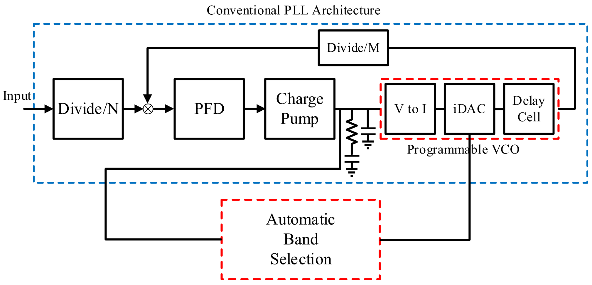
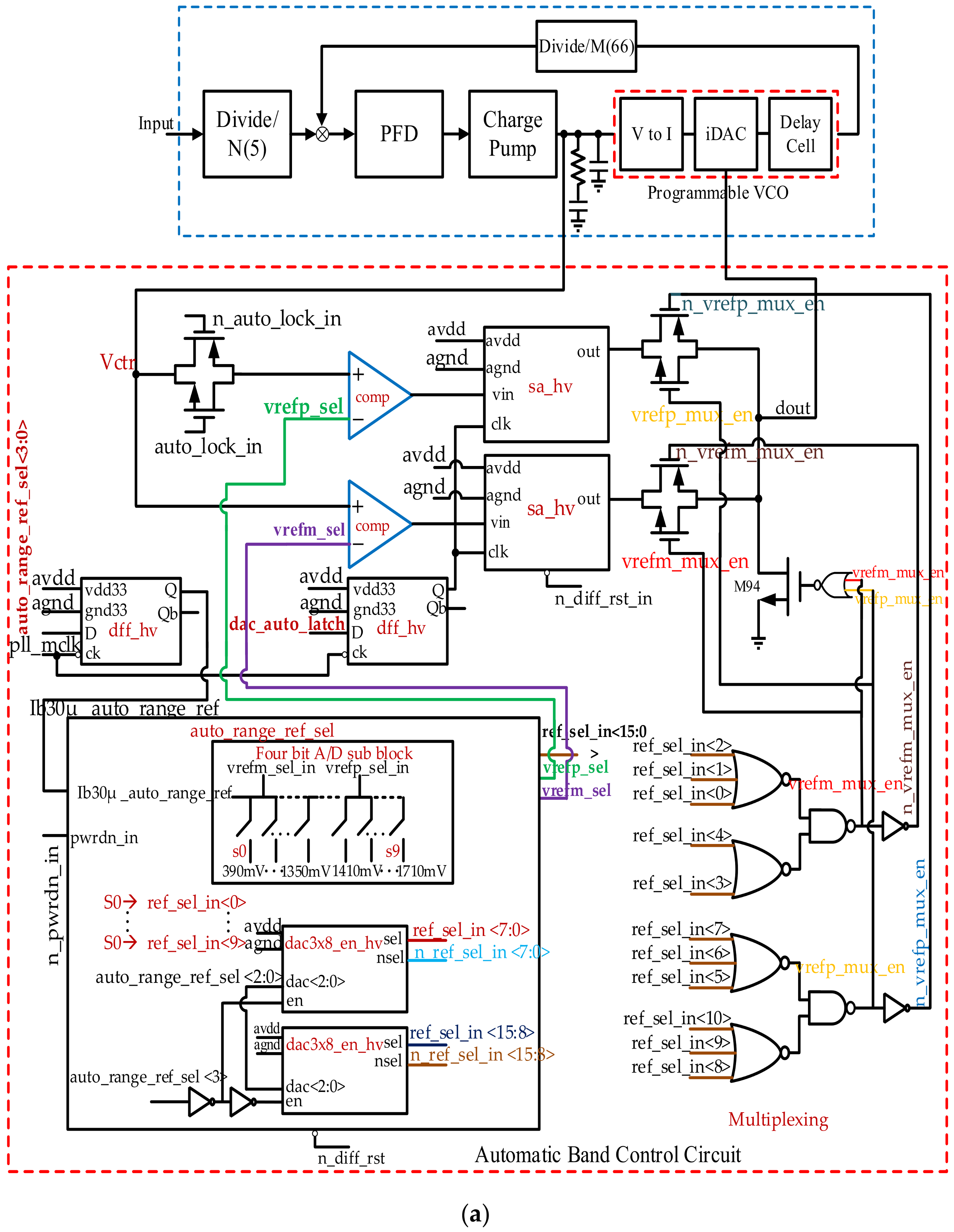
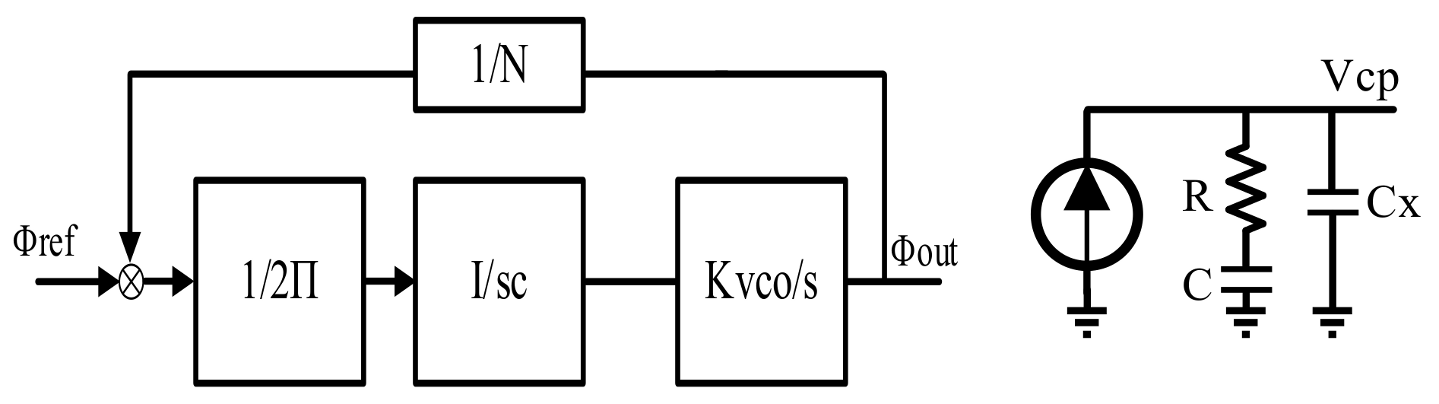
2. Proposed PLL Architecture

The classical PLL with the newly introduced circuit block to optimize the conventional architecture is shown in Figure 1. It consists of a reference frequency divider at the input, phase frequency detector (PFD), charge pump, passive loop filter, programmable VCO and automatic band selection circuit. A quartz crystal with a 25 MHz frequency is used as the reference frequency. It is further divided by a multi-modulus frequency divider, N = 5, to generate a 5 MHz reference frequency. The multi-modulus frequency divider is used at the feedback loop M = 66 to match the VCO central frequency with the input reference frequency. The PFD senses the phase difference, and, consequently, the charge pump generates an error current, which charges or discharges the loop filter. After filtering the high-frequency component, a DC control voltage Vctr is received at the input of the VCO. The VCO is replaced with a programmable VCO. The proposed VCO contains a voltage-to-current (V to I) converter with a programmable current digital to analog converter (iDAC) and a four-stage differential ring oscillator as the delay cell. The programmable iDAC is used to optimize the VCO delay cells. The programmable VCO is aided in its operation by the automatic band selection block. The inclusion of auto-ranging and a multiband selection circuit converts a classical PLL into a programmable PLL. It renders the programmable PLL capable of automatically adjusting the nominal center frequency of the VCO to an optimum required value suitable to operate over a wide frequency range. The proposed PLL architecture with a detailed automatic band selection circuit block is shown in Figure 2. On execution, it continuously monitors two important upper band voltages and lower band voltages with DC control voltage Vctr to remain in the desired frequency range. Its sub-block implementation and operation procedure are discussed in the following sections.

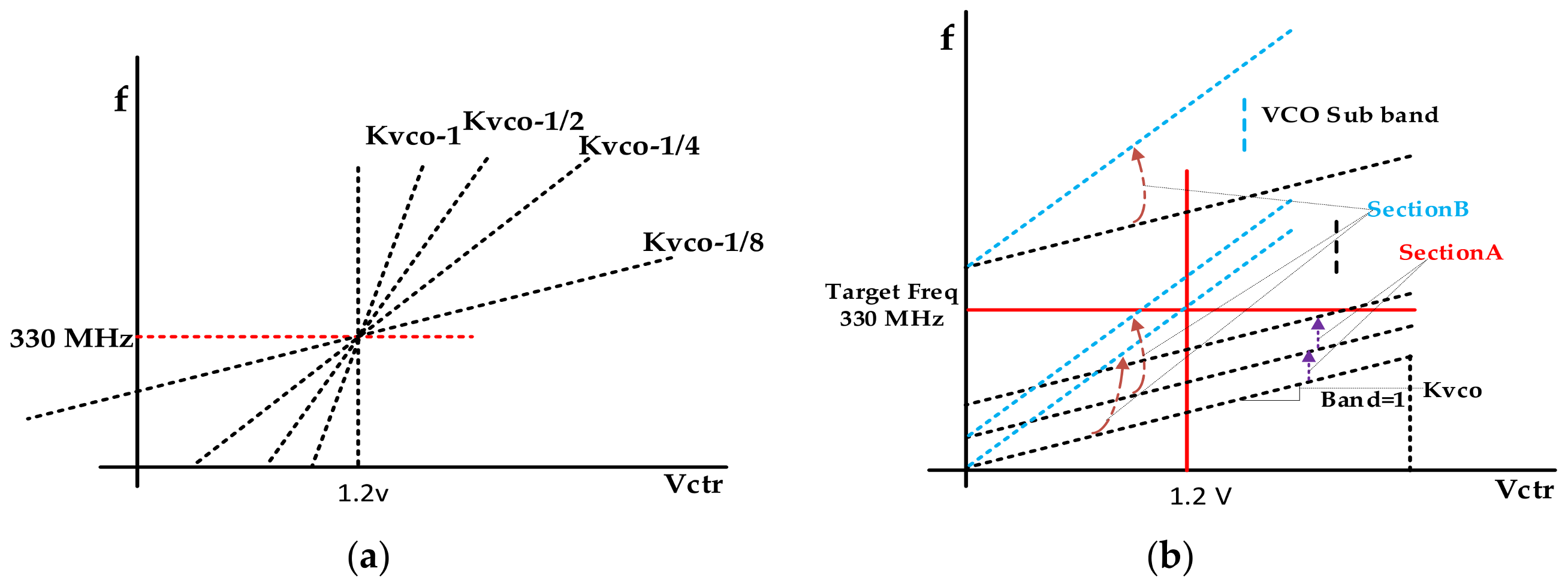
2.1. PLL Automatic Band Selection Circuit Block

The automatic band selection circuit block contains 3 × 8 decoders to select 11 voltage reference levels. These voltage levels are implemented by a resistive divider circuit shown in Figure 2b. It also contains a multiplexing circuit and a regenerative latch, followed by a dynamic comparator. The operation of the automatic band selection circuit is implemented by a four-bit ADC and digital control ASIC. The digital control ASIC is the integral part of the automatic band selection circuit. It sends an instruction sequence to generate a digitally controlled algorithm for the automatic band selection circuit to select various voltage levels for the comparison with Vctr. The digital control ASIC ensures a wide frequency operation range and applies self-calibration, whenever the VCO appears to cross frequency limits and to be unable to lock in the present frequency range.

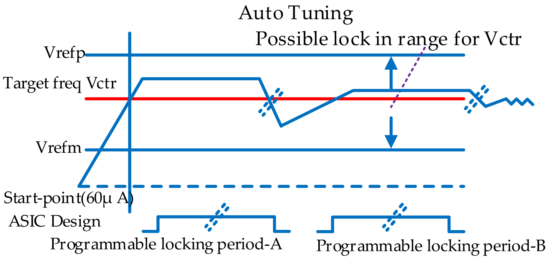
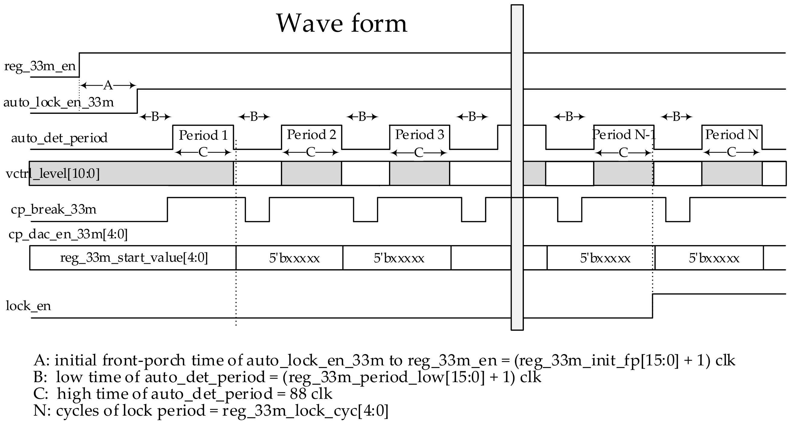
2.2. Band Selection Procedure

Band selection execution is implemented by the proposed circuit block realization shown in Figure 2a. As shown in the schematic diagram, the four-bit ADC architecture is implemented to generate the 11 reference voltages by using a resistor network and transmission gates. Here, two non-equal customized resistor values are implemented in the divider network to produce the two most probable reference voltage ranges. These two unique voltage levels’ resistive circuit is shown in Figure 2b, while the customized voltage values are displayed in Figure 3. Two 3 × 8 decoders were designed to select any one of the 11 reference voltages by enabling the ASIC digital control. One PMOS input pair comparator for a low-range reference voltage and one NMOS input pair comparator for a high-range reference voltage were designed with a hysteresis of 5 mV. These two dynamic comparators compare reference voltages with the DC control voltage Vctr. The comparator output moves to the regenerative latch to strengthen the logic value. To make the circuit compact, two comparators compare the Vctr and reference voltage levels vrefp_sel and vrem_sel multiplexed with eleven voltage levels. Eleven clock cycles are applied sequentially to compare all subdivided voltage reference levels and then obtain the final output voltage at dout.
Based on the comparator signal, the band moves/switches to the upper or lower frequency band or may remain in its present frequency band, if Vctr is among Vrefm_sel and Vrefp_sel. There are eleven voltage levels from 390 mV to 1.7 V as reference voltages in the ADC sub-block, out of which two indigenous voltage steps of 420 mV were designed along with the other 60 mV steps for the fast locking of the PLL, with the flexibility of a wide range selection.
In the case that PLL power down is observed for the Vctr, there may be an output at the dout. To overcome this unwanted condition, the circuit block comprises an NMOS, and an NOR gate is implemented at the output (dout), whose inputs are connected with the multiplexing output and ensure a ground path for the Vctr. Hence, based on ASIC mapping, these outputs (dout) move to the iDAC and provide a suitable change in the bias voltage of the delay cell. In the proposed PLL, the most probable locking voltage range is 0.7–1.7 V. The complete locking mechanism is displayed in Figure 4 along with the band selection simulation in Figure 5. In Figure 5, the automatic band selection simulation graph shows the ringing of the DC control voltage and the final convergence. It sequentially compares all eleven voltage references represented by the DAC data latch for one cp_break_d high pulse, then Vctr increases, and the pattern repeats until achieving the final lock-in range.

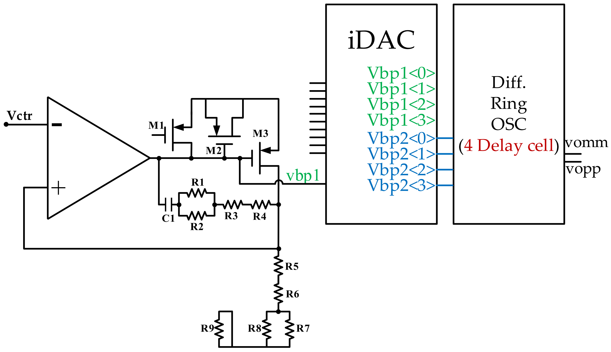
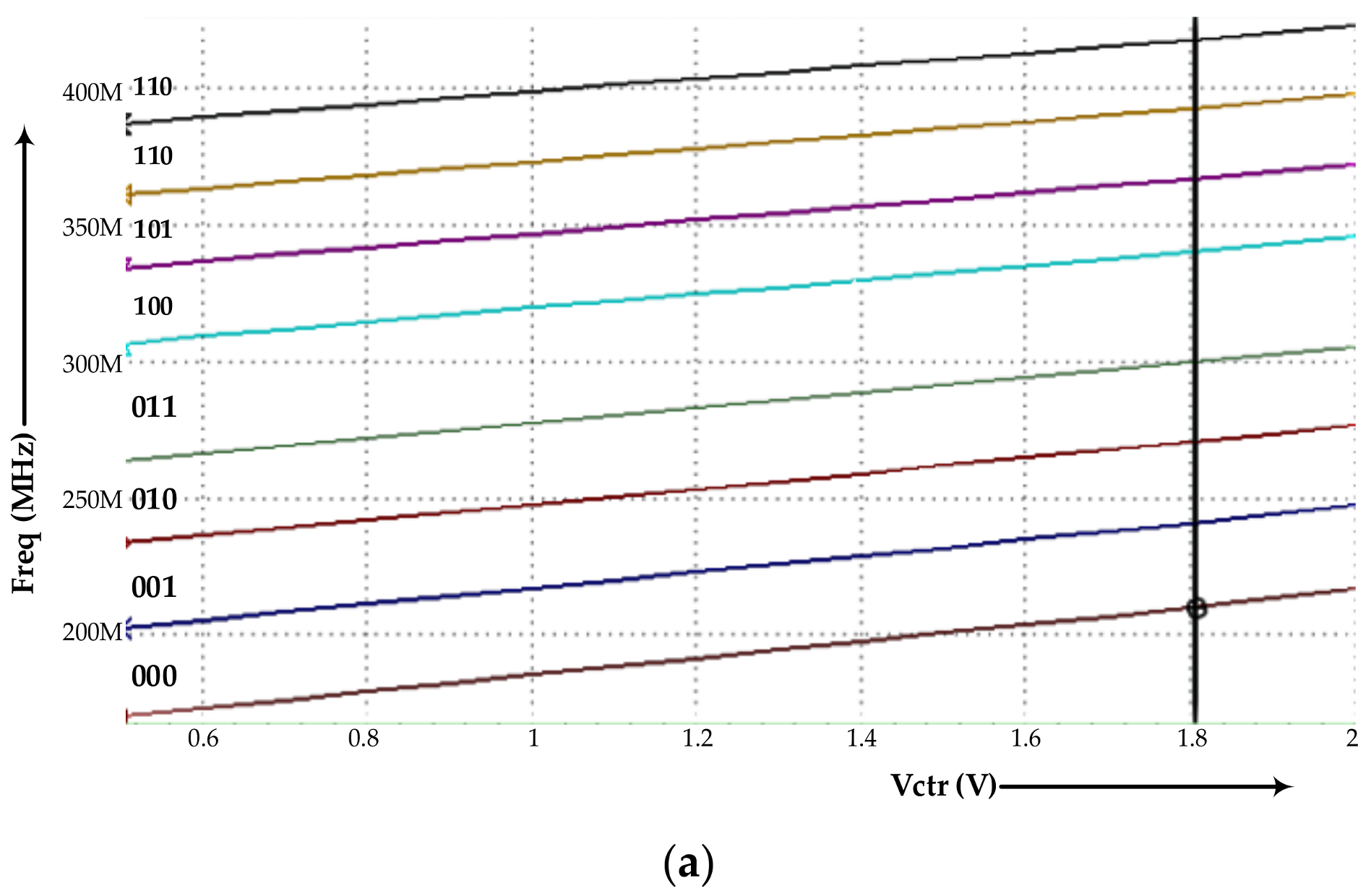
2.3. Programmable VCO Circuit

In the proposed PLL architecture, the VCO is tunable, meaning that its output frequency can be optimized based on the change in the input control voltage.
As we know for the VCO output,
ωout = ωo + Kvco.Vctr
Here, the proposed VCO contains a voltage-to-current (V–I) converter with a programmable iDAC and a four-stage differential ring oscillator as the delay cell. The V–I converter provides a linear relationship between the output current and the control voltage. As Vctr increases, there is a corresponding increment in the output current, and bias Vbp1 is observed with a constant resistor value. The programmable iDAC is used to optimize VCO delay cells by increasing or decreasing the tail current for a change in bias Vbp1<0:3> and Vbp2<0:3> values. A VCO with sub-blocks is shown in Figure 6.

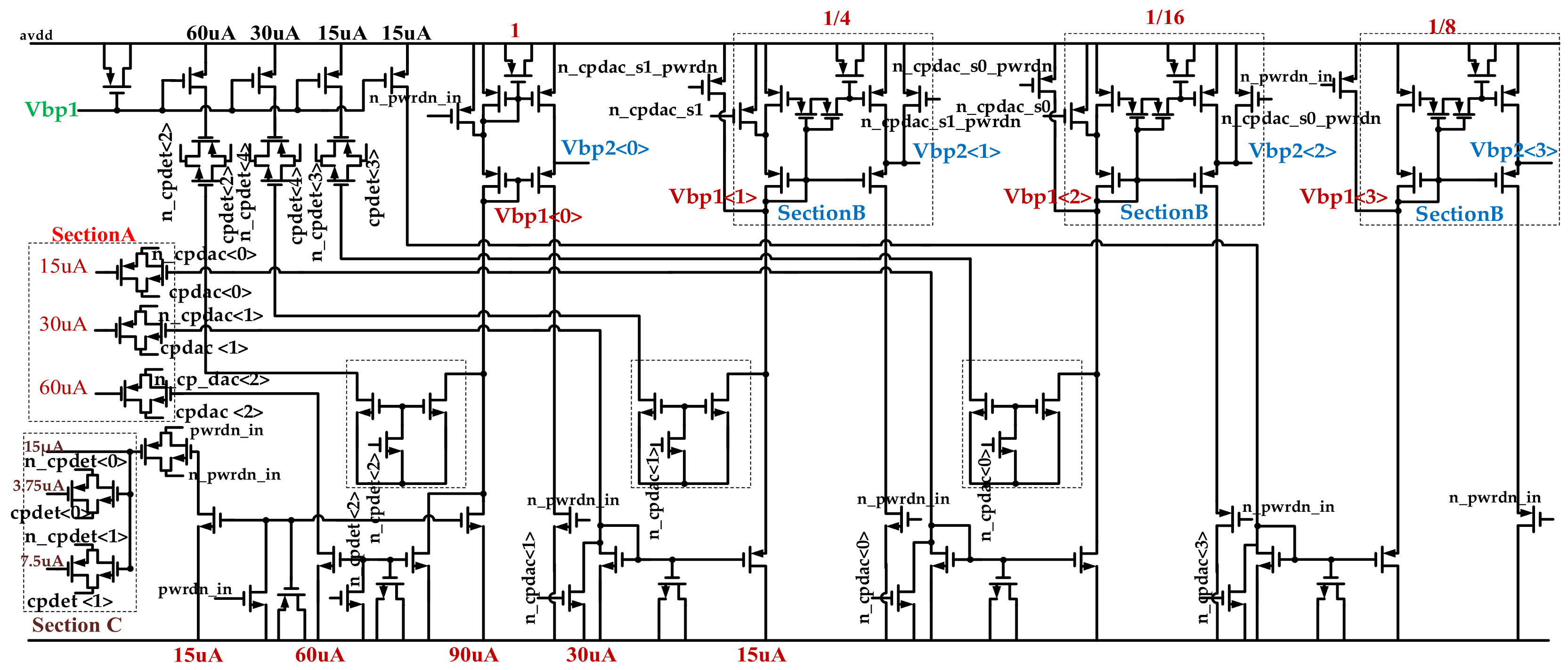
2.4. Programmable Current DAC for Wide Frequency Range Selection

Kvco is a VCO frequency/voltage gain having the unit of Hz/V. It measures how much the VCO output frequency changes relative to the VCO input control voltage Vctr change. Kvco is the slope of the curve of frequency vs. Vctr. For a high Kvco, fast settling with higher jitter occurs. It also creates loop stability and accuracy degradation. On the other hand, a very small Kvco value results in a slow VCO response and a narrow output frequency range. Hence, by dividing the target frequency into several sub-bands, each band’s Kvco can be reduced. This results in small jitter without sacrificing the required frequency range.
The programmable VCO is optimized by a 3-bit current DAC, which contains a weighted current mirror in section B to generate multiple current values. By using the weighted current mirror, the Kvco gain can be controlled, as with Kvco-1, Kvco-1/4, Kvco-1/8 and Kvco-1/16. It also operates as a DC current into the V–I converter. The programmable iDAC is the most important circuit block of the VCO to obtain a low Kvco gain through multiple VCO bands. The automatic band selection circuit output moves into the iDAC and provides the required change in the bias voltage Vbp2. From Figure 7, Vbp2<0:3> along with Vbp1<0:3> optimizes the delay cell tail current. As we can see in Figure 8a, section B provides multiple band twisting options for retaining a low VCO Kvco gain such as Kvco-1, Kvco-1/4, Kvco-1/8 and Kvco-1/16, while section A further adjusts the Kvco by providing band hopping to obtain the desired centralized frequency operation range.

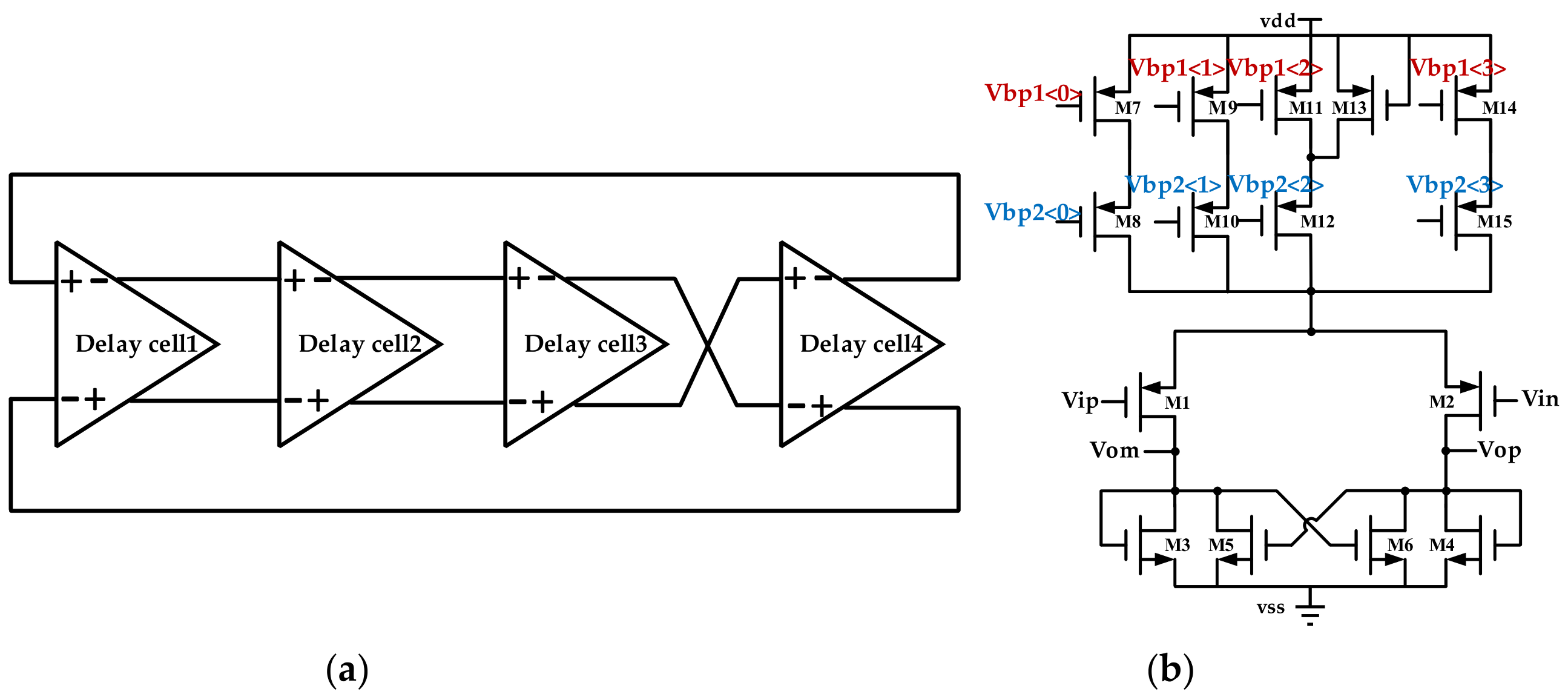
2.5. Four-Stage Differential Ring Oscillator and Delay Cell

The programmable VCO has a four-stage differential ring oscillator for low noise and low power supply applications, as shown in Figure 9a. The circuit of the proposed delay cell of the differential ring oscillator is shown in Figure 9b. The differential pair of PMOS transistors M1 and M2 acts as the input stage of the delay cell, and the tail current is provided by the different options of the bias voltage generation. The active loads are composed of a pair of NMOS transistors, M3 and M4, and a pair of cross-coupled latches, NMOS transistors M5 and M6.

2.6. s-Domain Analysis

A second order loop filter is implemented to avoid the unwanted ripple occurrence because of the exponential charging of C. The system will oscillate as there is just two integrators, hence the need to add a zero in the system to make it stable by placing an R in series with C [1,17,18,19,20,21,22,23,24]. There is another Cx placed to suppress the jumpy response of the series RC network during charging and discharging. A s-domain analysis block diagram is shown in Figure 10.
  • Open loop gain:
A = I 0 2 π · k s 2 C + C X · 1 + s C R 1 + s C 1 R
Closed loop gain:
r e f o u t = 1 + s C R 1 + s C R + s 2 C + C X 2 π I 0 K + s 3 C + C X C 1 R 2 π I 0 K
The proposed architecture obtains a phase margin of 60°, with C = 600 pF, Cx = 42 pF and R = 24.3 kΩ. Hence, it is a stable system. For a clock synthesizer with a VCO of the frequency range 330 MHz, the feedback divider M in the loop equations is 66 times.

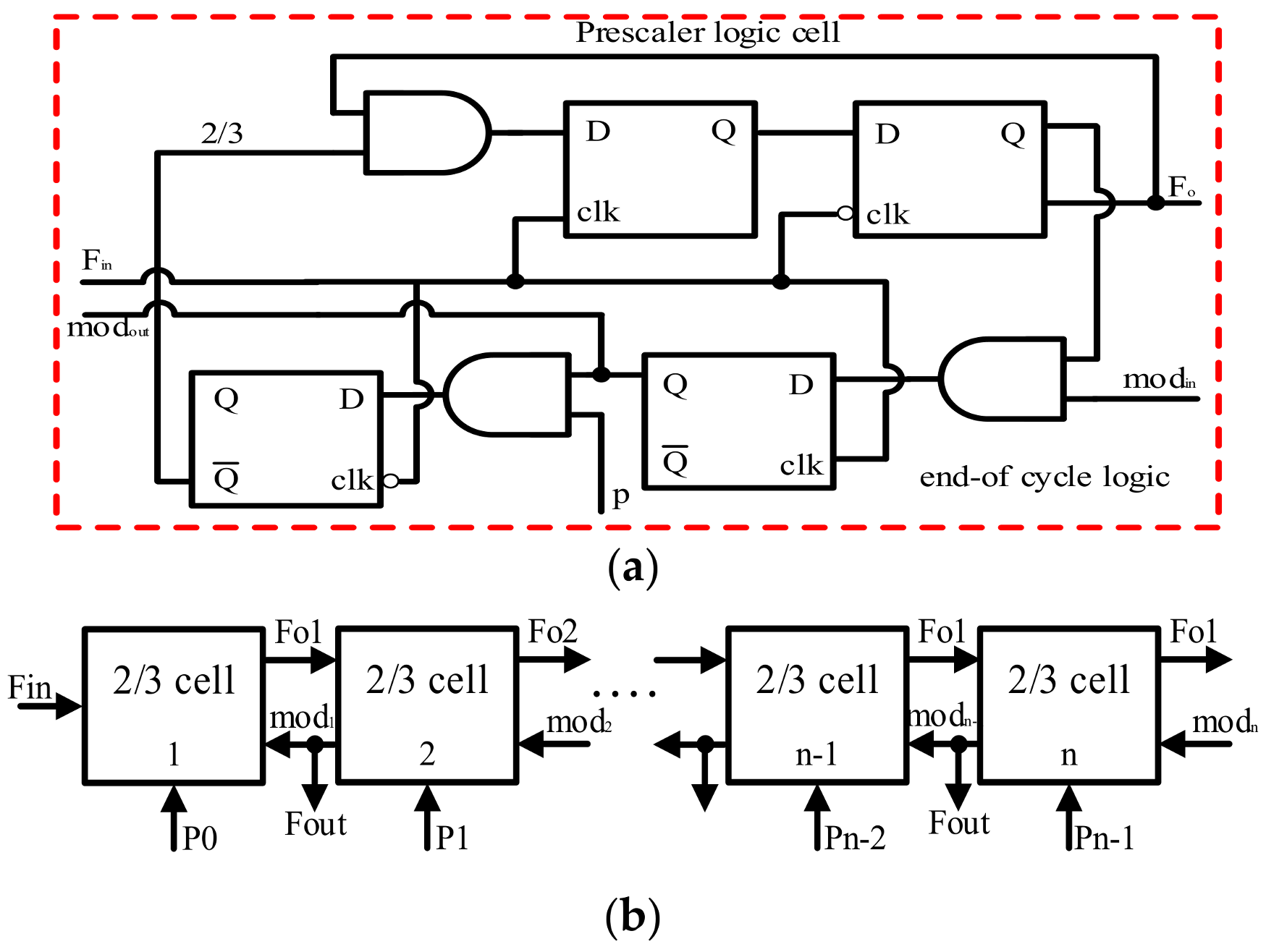
2.7. Programmable Prescaler for 32/33 Divider Ratio

In the proposed PLL, the frequency divider is N = 5 at the input and M = 66 in the feedback loop. A programmable prescaler is used for the frequency divider circuit. Figure 11a shows a dual-modulus prescaler circuit block that could divide by N or N + 1 according to the external control [2,3,4,5]. Here, a dual-modulus prescaler cell is implemented to allow the multi-moduli frequency divider at the input, as well as at the feedback loop, to produce an output frequency equal to the reference frequency. The multi-modulus divider provides flexibility to the PLL architecture and maintains the future relevancy.
The multi-modulus divider architecture is depicted in Figure 11. It consists of a chain of divide-by-2/3 dual-modulus prescalers in a cascade, connected similarly to a ripple counter. In every division period, the last cell of the dual-modulus prescaler in the chain generates signal modin−1. The signal then propagates up the chain. Its simulation is shown in Figure 12.

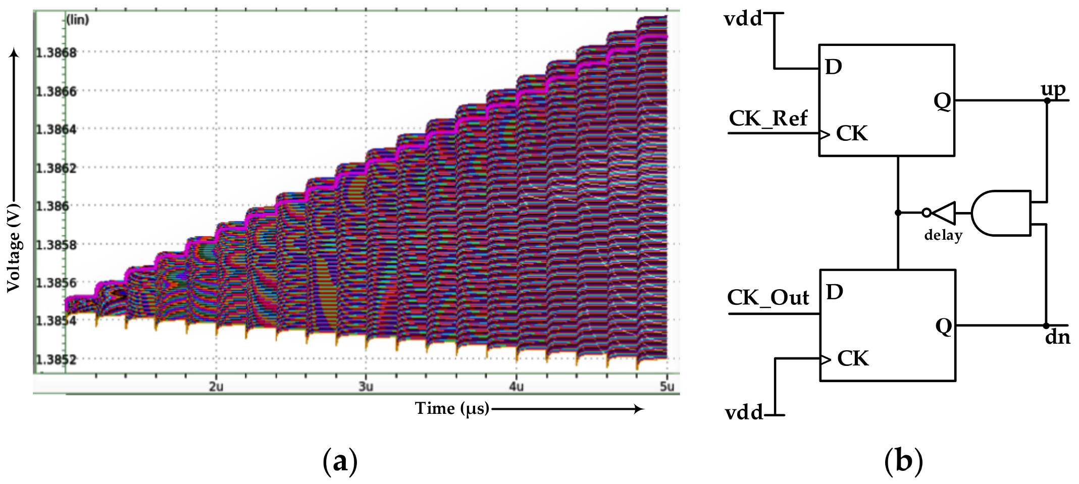
2.8. Phase Frequency Detector (PFD)

A PFD compares the rising/falling edge difference between the reference and feedback signals; thus, it can extract not only the phase difference but also the frequency difference. As a PFD detects the phase difference between the reference and the feedback frequency, when there is zero phase difference, it may go into a dead zone. In this condition, the charge pump cannot be fully turned on. In the proposed PLL architecture, the PFD has a dead zone voltage of less than 10 pV, as shown in Figure 13; still, a delay block of the inverter chain is used, having a delay from 0.9 to 2.6 ns in reset to avoid/minimize the unwanted dead zone.
The charge pump requires 1 μs for the Vctr settling after the PFD is off due to the unavoidable I_up and I_dn tail current mismatch. Figure 14 shows the delay setting and inverter chain delay to avoid the dead zone.

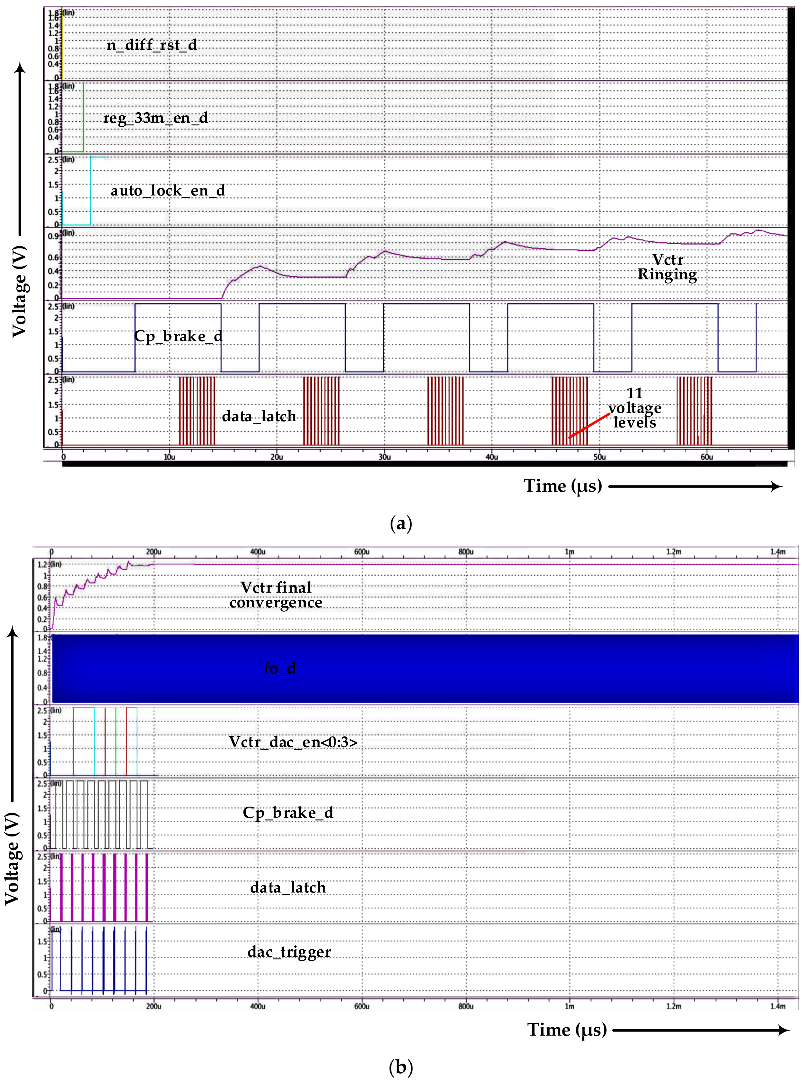
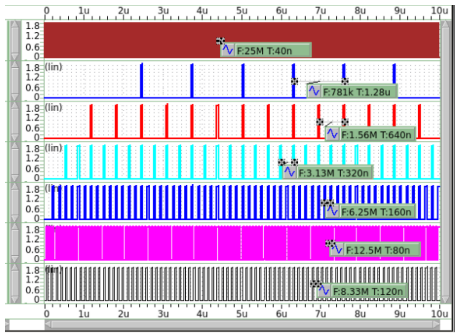
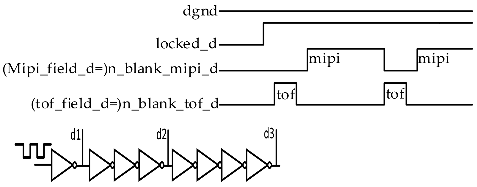
2.9. PLL Locking Operation Sequence Waveform

The PLL locking timing sequence instruction waveform is generated with a digital control ASIC. The locking operation is shown in the following Figure 15. As shown in the diagram, A is the initialization period before enabling PLL locking. It takes some time to initialize all the biasing and to provide a sufficient time margin to all the transition points. When cp_break_33 m is high, then the loop is broken and obtains a stable output frequency, compared with the ASIC block, where the feedback and control of the iDAC change. After this first step, cp_break_33 m moves down, and the loop will continue and use the changed iDAC value to settle. After a certain period of locking, the ASIC compares the frequency again. The process continues several times until reaching a locking value.

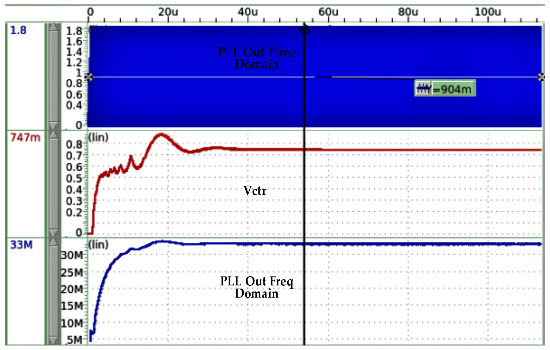
3. Simulation Results

The VCO output frequency with multiple bands is shown in Figure 16a. The Vctr range is 0.4–2.1 V, with a VCO tuning range of 0.84 V. The center frequency of the designed VCO is 330 MHz, with a variation absorption of ±10%, i.e., 297–363 MHz. The frequency sub-band step size is 8.25 MHz, with an average Kvco of 23 MHz. To ensure the wide-range frequency continuity, the two adjacent bands are overlapped with each other up to 30%. Figure 16b depicts a typical VCO gain characteristic at a typical 010 frequency sub-band case.
Figure 17 shows the whole PLL closed-loop output and lock-in timing. After convert-ing the time domain output into the frequency domain, the graph shows a stable 33 MHz output frequency.

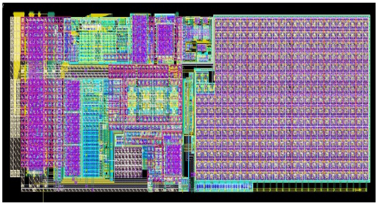
Chip Layout and Results
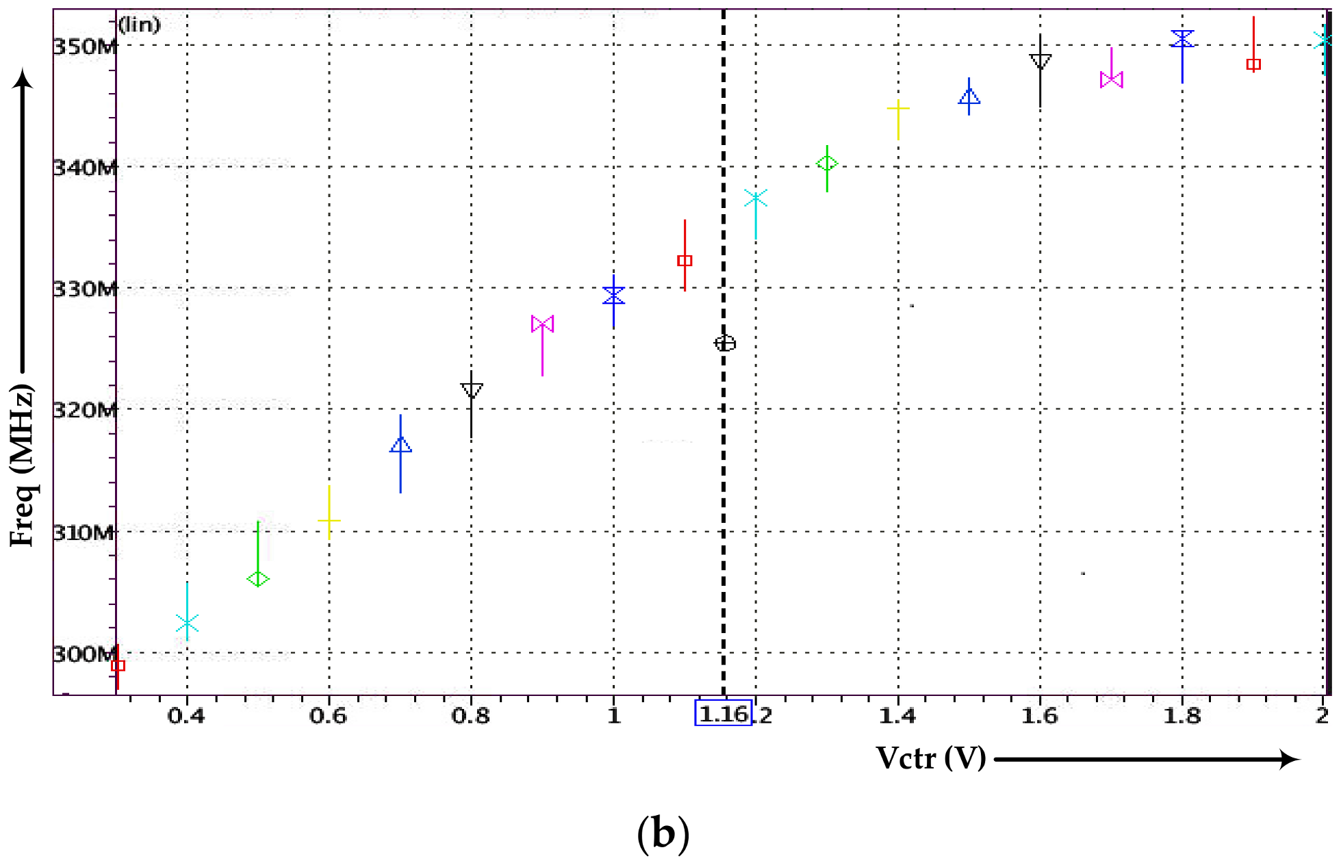
This chip was fabricated in the TSMC 0.18 μm 1P6M process. The new proposed PLL architecture’s complete and compact layout is shown in Figure 18. Its dimensions are 379.765 × 1325.115 μm. The measurement was carried out at the CIC (National Chip Implementation Center).
Table 1 and Table 2 summarize the performance of the PLL architecture.

4. Measurement

This section presents the proposed PLL output measurement results including the duty cycle and the frequency standard deviation. The PLL measurement setup is shown in Figure 19a–c.

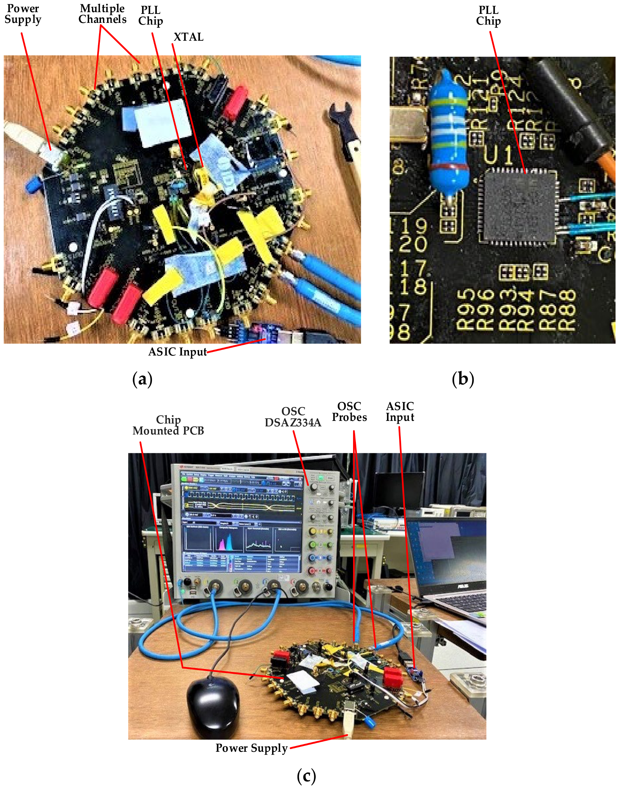
4.1. Printed Circuit Board for Measurement

In high-speed chip measurement, the ideal and optimum method is to use a high-speed probe directly on the chip pad. However, due to the large number of pads on the chip, it is difficult to directly probe which requires a wider pad spacing. Therefore, a printed circuit board (PCB) is used in measurement to provide the path for the DC power, bias voltage, bias current, digital control signal and also the input/output signal. As the power supply is placed at a distant position, a capacitor is necessarily added on the PCB to eliminate the noise. In Figure 19a, the printed circuit board with its important components is shown. It contains a quartz crystal for the reference frequency, PLL chip, ASIC input, multiple channels and a supply input.
The SMA connectors are used to monitor the 33 MHz signal, and also for the input reference frequency. The chip is mounted in the middle of a hexagonal PCB to maintain an equal distance from all channels. Bonding wires are used to connect the chip pads and PCB pads. The PCB is made of FR4 material. To eliminate the reflection along its path, 50Ω transmission lines were designed to match the equipment impedance.

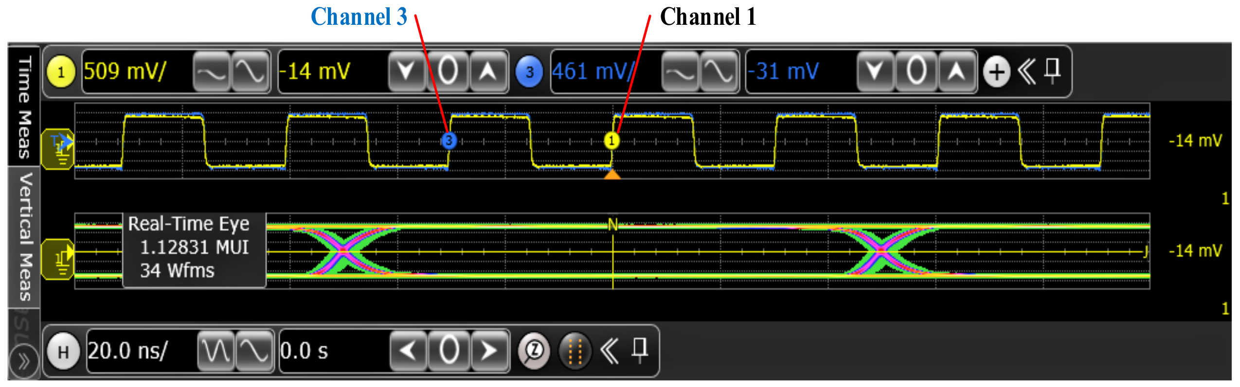
4.2. Measurement Results

Figure 19c shows the complete setup overview of the measurements. The chip was measured by a DSAZ334A Infiniium Oscilloscope with a 20 GSa./s sample rate and up to 4,194,304 pts memory depth per channel feature. The oscilloscope was well calibrated and enabled measuring 6-bit pattern length. Using this oscilloscope, we measured PLL output. Figure 20 shows the PLL output and the corresponding eye diagram. For two rising edges, the measured values of channel 1 (point1) and channel 3 (point 3) are 509 mV with an offset of −14 mV, and 461 mV with an offset of −31 mV, respectively. Table 3 summarizes the measured duty cycle and frequency with standard deviation. The eye diagram in Figure 20 also provides all jitter value information, which is summarized in Table 4. Figure 21a depicts the bathtub histogram for the total jitter (TJ) with a bit error rate of (1E-12), while Figure 21b shows a Gaussian profile for the random jitter (RJrms,narrow).
The bathtub curve slope continuity and smoothness along with Gaussian distribution profile show absence of cross talk in the measured jitter.
Table 4 includes the TJ with a bit error rate of (1E-12), RJrms,narrow, the periodic jitter rms value (PJrms) and the duty cycle distortion (DCD). RJ is also known as unbounded jitter, while PJ and DCD are known as bounded jitter. PJ and DCD are parts of deterministic jitter. The total jitter TJ comprises deterministic (bounded) jitter and random (unbounded) jitter. RJrms,narrow measured value is 19.10 ps. The low random jitter ensures precise and stable clock generator application of proposed PLL. This is a spectral jitter measurement, which has more accuracy at critical low cross-talk. Abbreviations are defined below.

5. Conclusions

In this paper, a PLL prototype with a programmable VCO and automatic band selection was presented. The PLL chip was fabricated using the TSMC 0.18 μm 1P6M process. The programmable VCO frequency output was 330 MHz, while a PLL output frequency of 33 MHz was achieved for an input reference frequency of 25 MHz. The PLL prototype is designed for wide-range frequency selection with a low VCO gain to obtain low jitter. The architecture provides multiple overlapped band switching, as well as band twisting, with a programmable current DAC to obtain the desired central frequency operation. The chip measurement results show a 19.10 ps rms jitter. The Gaussian histogram and smooth bathtub curve show no cross-talk. The prototype also has an additional safety feature of a power down mode. It was shown that a differential design approach also reduces noise, possibility in the analog block. The proposed PLL is designed for −40 to s85 °C, a wide temperature range.

Author Contributions

Conceptualization, N.A. (Neeraj Agarwal); formal analysis, N.A. (Neeru Agarwal); methodology, N.A. (Neeraj Agarwal) and N.A. (Neeru Agarwal); supervision, C.-W.L.; validation, C.-W.L.; visualization, M.O.-e.; writing original draft, N.A. (Neeraj Agarwal); writing review and editing, N.A. (Neeru Agarwal), and C.-W.L. All authors have read and agreed to the published version of the manuscript.

Funding

This work was supported, in part, by grants from the Ministry of Science and Technology, Taiwan, under Grants MOST 108-2221-E-007-094-MY2,108-2622-M-007-006-CC1 and 109-2622-M-007-007-CC1.

Acknowledgments

The authors express their best thanks to Tyrafos Technology Company, Ltd., Taiwan, for providing facilities, and for the continuous encouragement, constant help, esteemed guidance and anonymous reviews about the manuscript. We are also thankful to the Chip Implementation Center (CIC), Taiwan, for the chip measurement and testing.

Conflicts of Interest

The authors declare no conflict of interest.

Abbreviations

PLLPhase-locked loop
KvcoVoltage-controlled oscillator gain
DACDigital-to-analog converter
PDFPhase frequency detector
PVT VariationProcess, voltage and temperature variation
ADCAnalog-to-digital converter
V to IVoltage-to-current converter
VctrVCO control voltage
PCBPrinted circuit board
DCDirect current
FinInput reference frequency
MHzMega hertz
NReference frequency divider ratio
MFeedback frequency divider ratio
FvcoVoltage-controlled oscillator frequency
FoutOutput frequency
CCapacitor
RResistor
fFrequency
IcpCharge pump current
KvcoVoltage-controlled oscillator gain
BWBand width
PMPhase margin
RjRandom jitter
rmsRoot mean square
BERBit error ratio
TIETime interval error

References

  1. Razavi, B. Design of Analog CMOS Integrated Circuits, 1st ed.; McGraw-Hill: New York, NY, USA, 2005. [Google Scholar]
  2. Best, R.E. Phase-Locked Loops, Theory Design, and Applications, 4th ed.; McGraw-Hill: New York, NY, USA, 1999. [Google Scholar]
  3. Razavi, B. Phase-Locked Loops, Design of Analog CMOS Integrated Circuit, 2nd ed.; McGraw Hill Education Private Limited: New York, NY, USA, 2002; pp. 532–576. [Google Scholar]
  4. Herzel, F.; Razavi, B. A study of oscillator jitter due to supply and substrate noise. IEEE Trans. Circuits Syst. II Analog Digit. Signal Process. 1999, 46, 56–62. [Google Scholar] [CrossRef]
  5. Best, R.E. Phase-Locked Loops, 1st ed.; McGraw Hill: New York, NY, USA, 2003. [Google Scholar]
  6. Chen, Z.; Wang, M.; Chen, J.X.; Liang, W.F.; Yan, P.P.; Zhai, J.F.; Hong, W. Linear CMOS LC-VCO Based on Triple-Coupled Inductors and Its Application to 40-GHz Phase-Locked Loop. IEEE Trans. Microw. Theory Tech. 2017, 65, 2977–2989. [Google Scholar] [CrossRef]
  7. Buonomo, A.; Lo Schiavo, A. A Study of Injection Locking in Dual-Band CMOS Frequency Dividers. IEEE Trans. Circuits Syst. I Regul. Pap. 2017, 64, 1225–1234. [Google Scholar] [CrossRef]
  8. Abidi, A.A. Phase noise and jitter in CMOS ring oscillators. IEEE J. Solid-State Circuits 2006, 41, 1803–1816. [Google Scholar] [CrossRef]
  9. Homayoun, A.; Razavi, B. Analysis of phase noise in phase/frequency detectors. IEEE Trans. Circ. Syst. I Regul. Pap. 2013, 63, 529–539. [Google Scholar] [CrossRef] [Green Version]
  10. Lanza, P.T., II; Shtessel, Y.B.; Stensby, J.L. Improved acquisition in a phase-locked loop using sliding mode control techniques. J. Franklin Inst. 2015, 352, 4188–4204. [Google Scholar] [CrossRef]
  11. Yang, C.Y.; Liu, S.I. Fast-switching frequency synthesizer with a discriminator-aided phase detector. IEEE J. Solid-State Circuits 2000, 35, 1445–1452. [Google Scholar] [CrossRef]
  12. Shin, S.; Lee, K.; Kang, S.-M. 4.2 mW CMOS frequency synthesizer for 2.4 GHz ZigBee application with fast settling time performance. In Proceedings of the 2006 IEEE MTT-S International Microwave Symposium Digest, San Francisco, CA, USA, 11–16 June 2006; pp. 411–414. [Google Scholar]
  13. Woo, K.; Liu, Y.; Nam, E.; Ham, D. Fast-lock hybrid PLL combining fractional-N and integer-N modes of differing bandwidths. IEEE J. Solid-State Circuits 2008, 43, 379–389. [Google Scholar] [CrossRef]
  14. Nonis, R.; Palumbo, E.; Palestri, P.; Selmi, L. A Design Methodology for MOS Current-Mode Logic Frequency Dividers. IEEE Trans. Circuits Syst. I Regul. Pap. 2007, 54, 245–254. [Google Scholar] [CrossRef]
  15. Chen, C.-C.; Tsao, H.-W.; Wang, H. Design and Analysis of CMOS Frequency Dividers With Wide Input Locking Ranges. IEEE Trans. Microw. Theory Tech. 2009, 57, 3060–3069. [Google Scholar] [CrossRef]
  16. Levantino, S.; Marzin, G.; Samori, C.; Lacaita, A.L. A Wideband Fractional-N PLL With Suppressed Charge-Pump Noise and Automatic Loop Filter Calibration. IEEE J. Solid-State Circuits 2013, 48, 2419–2429. [Google Scholar] [CrossRef]
  17. Kong, L.; Razavi, B. A 2.4 GHz 4 mW Integer-N Inductorless RF Synthesizer. IEEE J. Solid-State Circuits 2016, 51, 626–635. [Google Scholar] [CrossRef]
  18. Venerus, C.; Galton, I. A TDC-free mostly-digital FDC-PLL frequency synthesizer with a 2.8–3.5 GHz DCO. IEEE J. Solid-State Circuits 2015, 50, 450–463. [Google Scholar] [CrossRef]
  19. Rajeshwari, D.S.; Rao, P.V.; Homayoun, A.; Razavi, B. On the stability of charge-pump phase-locked loops. IEEE Trans. Circuits Syst. I Regul. Pap. 2016, 63, 741–750. [Google Scholar]
  20. Lei, F.; White, M.H. Reference injected phase-locked loops (PLL-RIs). IEEE Trans. Circ. Syst. I Regul. Pap. 2017, 64, 1652–1660. [Google Scholar] [CrossRef]
  21. Wang, S.-F.; Hwang, T.-S.; Wang, J.-J. Phase-locked locked design with fast-digital-calibration charge pump. Int. J. Electron. 2018, 104, 898–912. [Google Scholar] [CrossRef]
  22. Jang, T.; Jeong, S.; Jeon, D.; Choo, K.D.; Sylvester, D.; Blaauw, D. A noise reconfigurable all-digital phase-locked loop using a switched capacitor-based frequency-locked loop and a noise detector. IEEE J. Solid-State Circuits 2018, 53, 50–65. [Google Scholar] [CrossRef]
  23. Ge, X.; Chen, Y.; Zhao, X.; Mak, P.-I.; Martins, R.P. Analysis and verification of jitter in bang-bang clock and data recovery circuit with a second-order loop filter. IEEE Trans. Very Large Scale Integr. VLSI Syst. 2019, 27, 2223–2236. [Google Scholar] [CrossRef]
  24. Nian, H.; Hu, B.; Wu, C.; Chen, L.; Xu, Y.; Blaabjerg, F. Analysis and reshaping on impedance characteristic of DFIG system based on symmetrical PLL. IEEE Trans. Power Electron. 2020, 35, 11729–11730. [Google Scholar] [CrossRef]
Figure 1. Block diagram of the proposed frequency synthesizer.
Electronics 10 01743 g001
Figure 2. (a) Proposed PLL with an automatic band selection circuit; (b) four-bit ADC sub-block with two indigenous custom voltage steps.
Electronics 10 01743 g002aElectronics 10 01743 g002b
Figure 3. Two major reference voltage levels vrefm_sel and vrefp_sel.
Electronics 10 01743 g003
Figure 4. Lock-in range for Vctr with the minimum and maximum Vref levels.
Electronics 10 01743 g004
Figure 5. Simulation results of (a) automatic band selection circuits (ringing) and (b) automatic band selection circuits (final convergence).
Electronics 10 01743 g005
Figure 6. VCO circuit sub-blocks.
Electronics 10 01743 g006
Figure 7. VCO circuit programmable iDAC.
Electronics 10 01743 g007
Figure 8. (a) Frequency vs. VCO tuning voltage; (b) frequency vs. VCO sub-band optimization.
Electronics 10 01743 g008
Figure 9. (a) Four-stage differential ring oscillator; (b) differential cross-coupled delay cell with multiband option.
Electronics 10 01743 g009
Figure 10. s-Domain analysis block diagram.
Electronics 10 01743 g010
Figure 11. (a) Prescaler logic cell; (b) multi-modulus divider architecture.
Electronics 10 01743 g011
Figure 12. Multi-modulus divider simulation (781 kHz–33 MHz).
Electronics 10 01743 g012
Figure 13. (a) PFD dead zone simulation; (b) PFD block diagram (delay inclusion).
Electronics 10 01743 g013
Figure 14. Inverter chain delay (0.3–0.9 ns).
Electronics 10 01743 g014
Figure 15. PLL locking instruction sequence.
Electronics 10 01743 g015
Figure 16. (a) VCO multiple bands; (b) VCO frequency vs. Vctr for 010 band.
Electronics 10 01743 g016aElectronics 10 01743 g016b
Figure 17. Transient simulation result for whole PLL.
Electronics 10 01743 g017
Figure 18. PLL layout (379.765 × 1325.115 μm).
Electronics 10 01743 g018
Figure 19. (a) PLL chip mounted on PCB; (b) PLL chip; (c) PLL measurement setup.
Electronics 10 01743 g019
Figure 20. Measured eye diagram.
Electronics 10 01743 g020
Figure 21. (a) Bathtub histogram (BER Tj Jitter); (b) Gaussian histogram (Rj Jitter).
Electronics 10 01743 g021
Table 1. Summary of PLL post-simulations.
Post_Simulation@TT_50 °C
Fin (MHz)25
N5
M66
Fvco (MHz)330
Fout (MHz)33
C (pF)600
Cx (pF)42
R (kΩ)24.3
Icp (μA)30
Kvco (MHz/V)23
BW18.1 KHz
PM (°)60
RJrms Jitter (ps)25
Table 2. Summary of PLL performance.
Process Technology180 nm
Power Supply1.8 V
Center Frequency 330 MHz
VCO Tuning Range0.84 V
Range of Control Voltage0.4–2.1 V
Kvco23 MHz/V
Modulus of Divider66
Reference Frequency25 MHz
Lock-in Time40 μs
VCO Gain23 MHz/V
Bandwidth18.1 KHz
Power Consumption2 mW
PLL Layout Area1.325115 × 0.379765 mm
Table 3. Summary of duty-cycle and frequency measurements for channel 1 (point 1) and channel 2 (point 3).
MeasurementCurrentMeanMinMax Range Std DevCount
Duty Cycle (1)50.10%50.00%49.80%50.30%450 m%62.6 m%235,276
Frequency (1)32.995145 MHz32.997494 MHz32.845768 MHz33.132852 MHz287.08341 KHz43.579266 KHz235,276
Frequency (3)33.016368 MHz32.997502 MHz32.821353 MHz33.161631 MHz340.27749 KHz46.565005 KHz325,269
Duty cycle (3)50.00%50.00%49.80%50.30%510 m%66.3 m%235,269
1 Period (3)32.28801 ns30.3053842 ns30.15533 ns30.46797 ns312.64 ps42.7670 ps235,269
1 Per-Per (3)4.22 ps−2.0 fs−2.97.72 ps230.76 ps528.48 ps82.1440 ps235,235
1 Per-Per (1)7.92 ps−2.2 fs−243.87 ps211.33 ps455.20 ps77.7530 ps235,242
1 Period (1)30.30749 ns30.3053838 ns30.18152 ns30.44532 ns263.80 ps40.0235 ps235,276
Table 4. Summary of Jitter measurements.
Measurement Value
SourceChannel 1
RJ MethodSpectral
Data Rate197.9856 Mb/s
Pattern Length6 bits
TJ(1E-12)347.43 ps
RJrms,narrow19.10 ps
DJδδ77.70 ps
Transitions376.002 k
PJrms21.35 ps
PJδδ77.70 ps
DDJpp0.0 s
DCD11.50 ps
ISIpp0.0 s
DDPWSn/a
F/2 (Even/Odd)n/a
Clock RecoverySecond Order
Edge DirectionRising
MeasurementTIE (Phase)
Publisher’s Note: MDPI stays neutral with regard to jurisdictional claims in published maps and institutional affiliations.

