Article

Word-Based Systolic Processor for Field Multiplication and Squaring Suitable for Cryptographic Processors in Resource-Constrained IoT Systems

1
Computer Engineering Department, College of Computer Engineering and Sciences, Prince Sattam Bin Abdulaziz University, Al-Kharj 16278, Saudi Arabia
2
Electrical and Computer Engineering Department, University of Victroia, Victoria, BC V8P 5C2, Canada
*
Author to whom correspondence should be addressed.
Submission received: 28 May 2021 / Revised: 22 July 2021 / Accepted: 23 July 2021 / Published: 25 July 2021
(This article belongs to the Special Issue Cyber Security for Internet of Things)

Abstract

:
Internet of things (IoT) technology provides practical solutions for a wide range of applications, including but not limited to, smart homes, smart cities, intelligent grid, intelligent transportation, and healthcare. Security and privacy issues in IoT are considered significant challenges that prohibit its utilization in most of these applications, especially relative to healthcare applications. Cryptographic protocols should be applied at the different layers of IoT framework, especially edge devices, to solve all security concerns. Finite-field arithmetic, particularly field multiplication and squaring, represents the core of most cryptographic protocols and their implementation primarily affects protocol performance. In this paper, we present a compact and combined two-dimensional word-based serial-in/serial-out systolic processor for field multiplication and squaring over GF( 2 m ). The proposed structure features design flexibility to manage hardware utilization, execution time, and consumed energy. Application Specific Integrated Circuit (ASIC) Implementation results of the proposed word-serial design and the competitive ones at different embedded word-sizes show that the proposed structure realizes considerable saving in the area and consumed energy, up to 93.7% and 98.2%, respectively. The obtained results enable the implementation of restricted cryptographic primitives in resource-constrained IoT edge devices such as wearable and implantable medical devices, smart cards, and wireless sensor nodes.

1. Introduction

Internet of Things (IoT) is a modern technology that connects a tremendous number of gadgets—such as smartphones, wearable devices, sensors, vehicles, and smart meters—to the internet [1,2]. It provides services and efficient solutions in numerous domains such as healthcare, smart cities, smart grid, industrial manufacturing, business management, logistics, smart homes, and intelligent transportation [3,4,5,6,7,8].
Security and privacy issues are the primary concern in most IoT-based systems. They prohibit its usage in most applications, especially healthcare applications. Accordingly, we should employ efficient and practical security solutions to protect the IoT-based systems. Therefore, cryptographic protocols should be applied at the different layers of the IoT framework, especially edge devices, to solve all security concerns. Most IoT edge devices have limited computing resources, which makes implementing traditional cryptographic algorithms, such as Rivest, Shamir, and Adleman (RSA) and Digital Signature Algorithm (DSA) [9], impractical. Due to its short-key sizes and enhanced computational efficiency, the Elliptic Curve Cryptographic (EEC) algorithm [10] becomes the cryptography choice for resource-constrained embedded devices such as mobile phones, smart cards, and environmental sensors. ECC’s essential operation is the point multiplication, which mainly depends on the basic finite field arithmetic operations of addition, multiplication, squaring, and division/inversion. The ECC processor’s overall performance primarily relies on the efficient implementation of these operations. Since the finite field multiplier is the basic building block of the other field operations of division/inversion and exponentiation, it is considered the fundamental building block of the ECC processor. Therefore, any slight improvement in its implementation results in a significant increase in the ECC processor’s whole performance.

1.1. Paper Motivation and Related Work

Field multiplication in GF( 2 m ) is very crucial in several field operations such as modular exponentiation and inversion/division as they are performed using a sequence of multiplications. Most of the previously reported multipliers over GF( 2 m ) have high area and time complexities that render their realization in resource-constrained IoT edge devices highly challenging [11,12,13,14]. Therefore, it becomes important to have multiplier architectures that target this type of applications. Word-serial multiplier architectures are reported in the literature to solve this problem. They have a trade-off between speed and area complexities and, thus, they provide the designer more flexibility to reach the desired design. The structures of word-serial multipliers are classified into four types: Serial-In/Serial-Output (SISO) structures, Serial-In/Parallel-Output (SIPO) structures, Parallel-In/ Serial-Output (PISO), and Scalable structures. The polynomial basis word-serial systolic multipliers using SISO structure are presented in [15,16,17,18,19]. The polynomial basis word-serial multipliers with the SIPO structure are reported in [20,21,22,23]. The word-serial type-T Gaussian normal basis (GNB) multipliers with PISO structure are reported in [24]. The scalable systolic multiplier structures are reported in [25,26,27,28,29,30,31].
Modular exponentiation is a fundamental part of cryptographic algorithms. There are two binary approaches used to compute modular exponentiation: the Most Significant Bit (MSB)-first approach and the Least Significant Bit (LSB)-first approach. In LSB-first approach, the modular multiplication and squaring operations can be executed concurrently to reduce the processing time. There are many attempts in the literature to combine the multiplication and squaring operations in a unified structure to increase performance and hardware utilization [13,14,32]. To the best of our knowledge, the suggested combined multiplier-squarer structures are dedicated for high-speed applications and do not target the resource-constrained applications.

1.2. Paper Contribution

In this paper, we propose a word-based two-dimensional SISO systolic processor for combined field multiplication and squaring over GF( 2 m ). The main difference between the proposed SISO architecture and the other types of word-serial multiplier architecture is that the proposed multiplier-squarer structure is extracted by using a systematic approach [33,34,35,36,37,38,39]. In contrast, the other word-serial multiplier structures are extracted conventionally without the use of specific methodology. The applied approach allows the designer to construct the design in the smallest size in order to fit all resource-constrained IoT edge devices that have more restrictions on area and power consumption. Moreover, it provides the flexibility in managing execution time and the consumed energy of these devices. Another advantage of the proposed SISO design over other word-serial conventional ones is that it provides a compact and unified structure that simultaneously performs multiplication and squaring operations. By contrast, the traditional design designs computes both operations sequentially. Moreover, it has a regular structure and local interconnections that render it more suitable for VLSI implementation.

1.3. Paper Organization

This paper can be organized as follows. Section 2 provides a brief explanation to the combined polynomial multiplication-squaring algorithm in G F ( 2 m ) . Section 3 develops its associated dependency graph (DG). Section 4 explains the explored two-dimensional word-based SISO systolic processor. Section 5 provides the area and delay complexities of the proposed design and the best of the existing word-serial designs. Section 6 concludes this study.

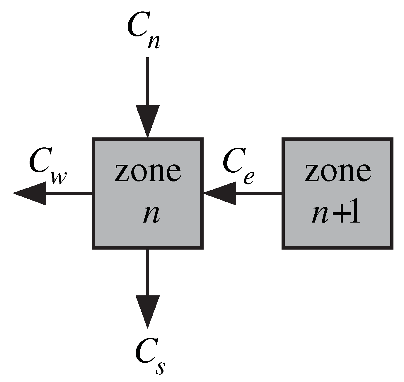
2. Combined Polynomial Multiplication-Squaring Algorithm in GF ( 2 m )

Let C ( x ) and D ( x ) be two polynomials in G F 2 m and G ( x ) be the irreducible polynomial in standard basis representation. These polynomials can be represented as follows:
C ( x ) = i = 0 m 1 c i x i
D ( x ) = i = 0 m 1 d i x i
G ( x ) = i = 0 m g i x i
where c i , d i , g i G F ( 2 ) .
The polynomial multiplication and squaring over G F ( 2 m ) can be defined as follows.
R ( x ) = C ( x ) D ( x ) mod G ( x )
Q ( x ) = C ( x ) C ( x ) mod G ( x )
The products R ( x ) and Q ( x ) can be calculated using the combined algorithm, Algorithm 1, proposed by Choi in [13]. This algorithm calculates three partial polynomials C ( x ) , R ( x ) , and Q ( x ) . Variables C i , R i , and Q i are used to indicate the values of C ( x ) , R ( x ) , and Q ( x ) at iteration i. d i 1 and c i 1 represent the ( i 1 ) t h coefficients of input polynomials D ( x ) and C ( x ) , respectively. The initial variables R 0 and Q 0 are assigned zero values and the initial variable C 0 is assigned the coefficients of input polynomial C ( x ) . In each i iteration of the for loop, the intermediate variables are updated as follows:
  • Variable C i is updated by shifting left C i 1 and by reducing using the irreducible polynomial G;
  • Variable R i is updated by multiplying C i 1 by coefficient d i 1 and by adding the obtained result to R i 1 ;
  • Variable Q i is updated by multiplying C i 1 by coefficient c i 1 and by adding the obtained result to Q i 1 .
Algorithm 2 is the bit-level representation of Algorithm 1. Variable c j + 1 i represents the ( j + 1 ) t h bit of C at the i t h iteration. Moreover, r j i and q j i represent the i t h bit of R and Q at the i t h iteration, respectively. Notice that j + 1 indicates that j + 1 is to be reduced modulo m.
Algorithm 1 Algorithm for multiplication and squaring over GF( 2 m ) [13].
  Input: C ( x ) , D ( x ) , and G ( x )
  Mult. Output: R ( x ) = ( C ( x ) . D ( x ) ) mod G ( x )
  Square Output: Q ( x ) = ( C ( x ) . C ( x ) ) mod G ( x )
  Initialization:
   R 0 0 , Q 0 0 , C ( 0 ) C ( x ) , D D ( x ) , G G ( x )
  Algorithm:
1: for 1 i m do
2:   C i = C i 1 . x mod G ( x )
3:   R i R i 1 + d i 1 C i 1
4:   Q i Q i 1 + c i 1 C i 1
5: end for
Algorithm 2 Bit-level algorithm for multiplication and squaring over GF( 2 m ).
  Input: C ( x ) , D ( x ) , and G ( x )
  Mult. Output: R ( x ) = ( C ( x ) . D ( x ) ) mod G ( x )
  Square Output: Q ( x ) = ( C ( x ) . C ( x ) ) mod G ( x )
  Initialization:
   R 0 = ( r m 1 0 r 1 0 r 0 0 ) ( 0 00 )
   Q 0 = ( q m 1 0 q 1 0 q 0 0 ) ( 0 00 )
   C 0 = ( c m 0 c 1 0 c 0 0 ) ( 0 c m 1 c 1 c 0 )
   D ( d m 1 d 1 d 0 )
   G ( g m 1 g 1 g 0 )
  Algorithm:
1: for 1 i m do
2:  for 0 j m 1 do
3:    c j + 1 i = c j i 1 + c m 1 i 1 g j + 1
4:    r j i = r j i 1 + d i 1 c j i 1
5:    q j i = q j i 1 + c i 1 c j i 1
6:  end for
7: end for

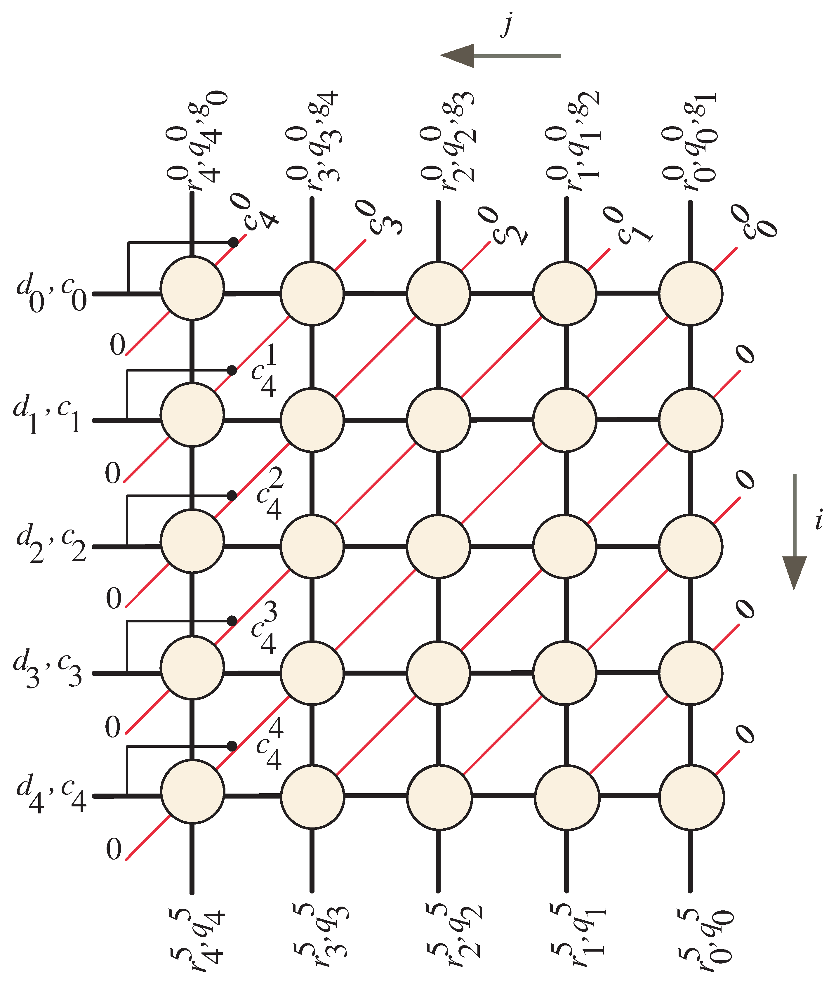
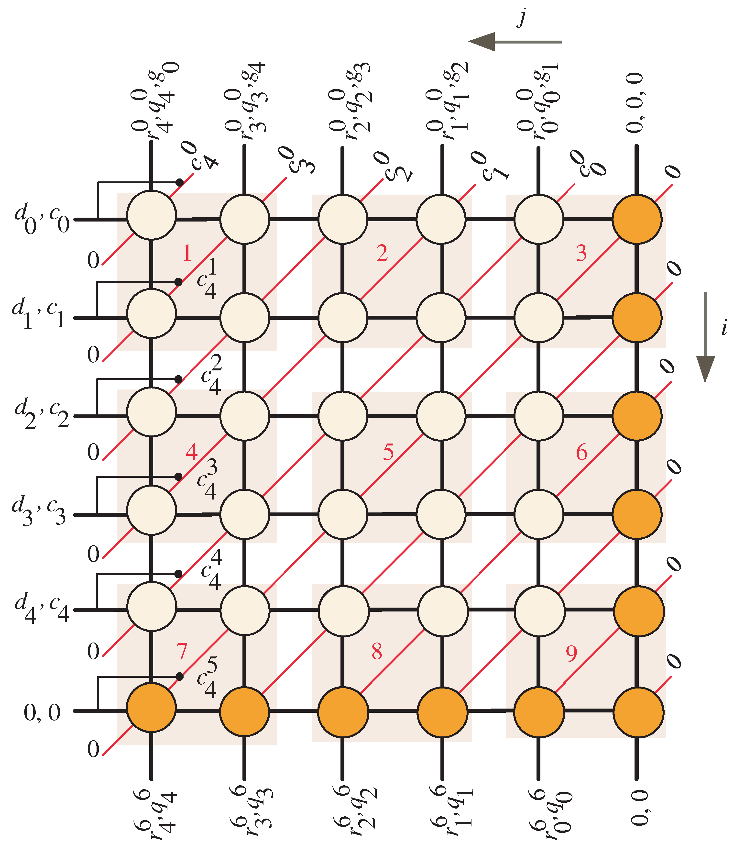
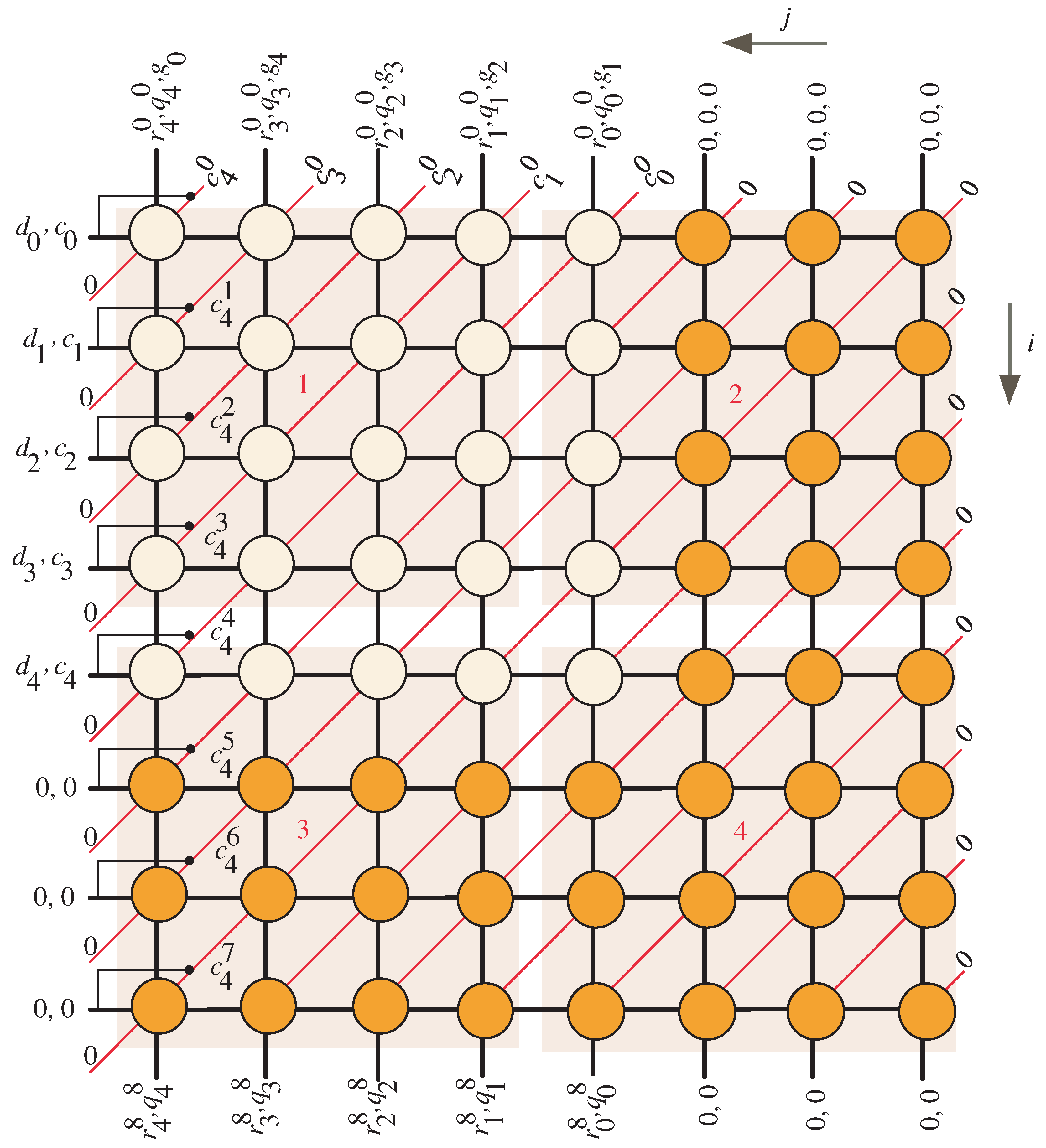
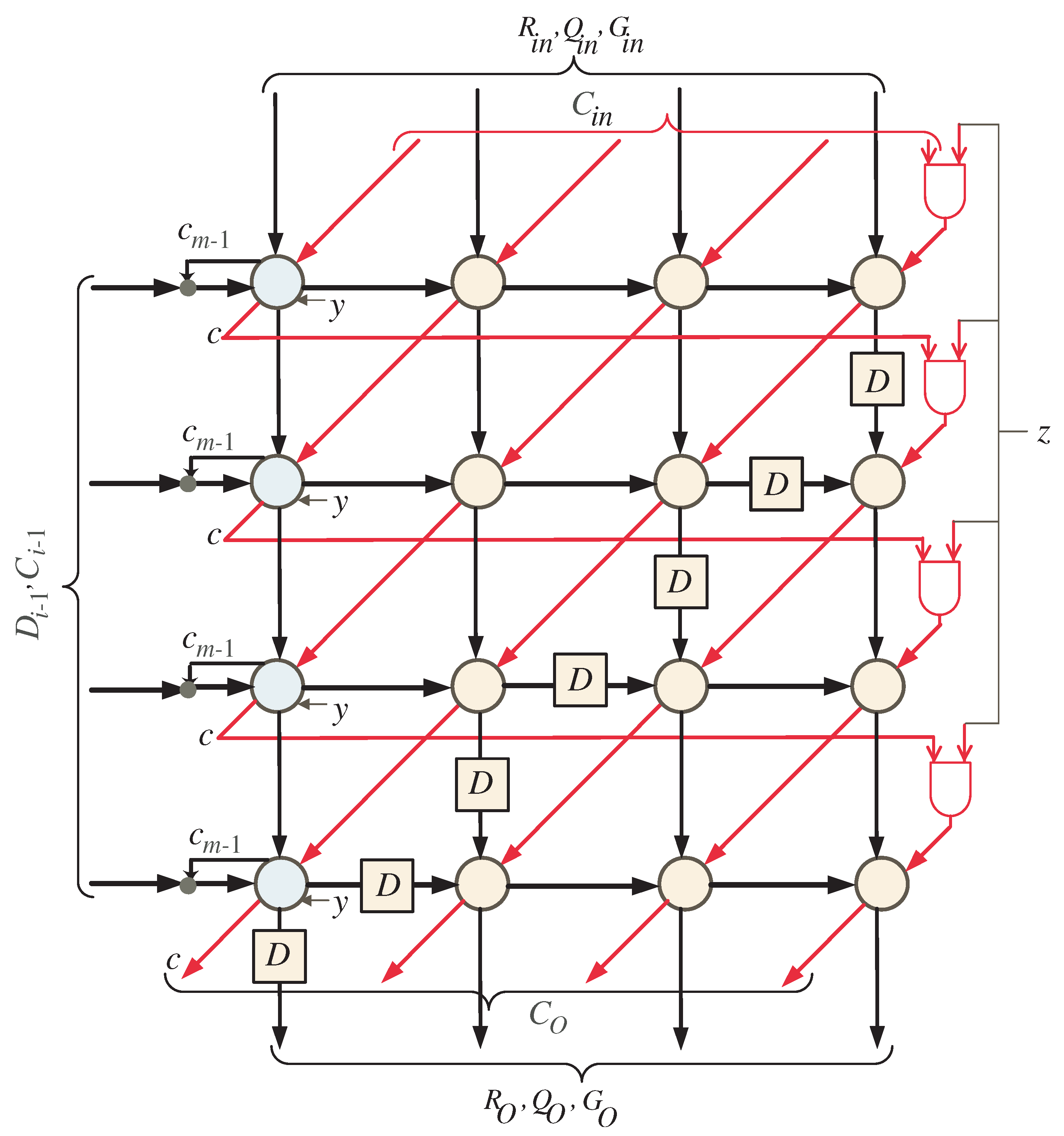
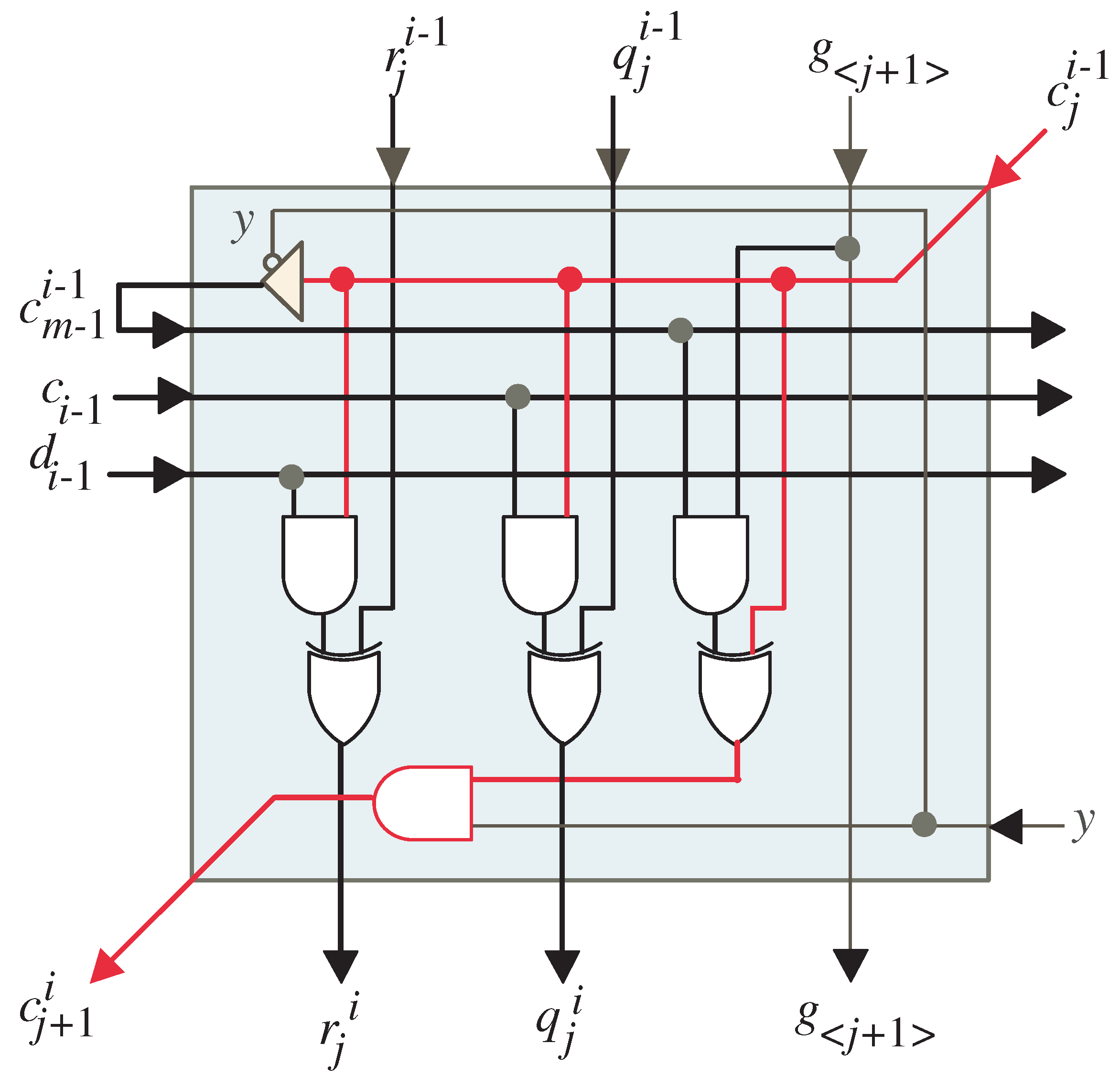
3. Algorithm Dependency Graph

Algorithm 1 is an example of a Regular Iterative Algorithm (RIA). The authors of [33] showed how to obtain the dependency graph (DG) of an RIA algorithm. Figure 1 shows the DG based on Algorithm 2 for combined polynomial multiplication-squaring in G F 2 m . The nodes in Figure 1 represent points in the two-dimensional integer domain D , with indices i and j indicating the rows and columns, respectively, and they possess the following ranges:
1 i m , 0 j m 1
The figure is for the case when m = 5 bits. The algorithm has three input variables C, D, and G and two output variables R and Q. Variables R, Q, and G are represented by the vertical lines. Variable C is represented by the slanted lines (red lines). Input bits c i 1 and d i 1 along with the resulting intermediate bits c m 1 i 1 are broadcasted horizontally. The initial bits r j 0 , q j 0 , c j 0 , and g j + 1 are inputs to the DG as shown at the top of Figure 1. The DG nodes (circles) execute the main operations of Algorithm 2 from steps 3 to 5. Output bits r j m and q j m are produced from the bottom of the DG as indicated in Figure 1.
The DG in Figure 1 can be used for design space exploration of the combined multiplication and squaring operations. The design exploration involves finding valid node scheduling functions and mapping or projecting the graph nodes to processing elements (PEs). Reference [33] explains how design space exploration could be performed by using affine and non-linear scheduling and projection functions.
The affine scheduling and projection functions cannot be used to explore word-serial systolic processors. Thus, our goal is to apply the non-linear scheduling and projection techniques discussed in [33] to the developed algorithm, Algorithm 2, in order to explore the most efficient two-dimension word-serial systolic processor that is able to satisfy any Input/Output (I/O) limitations/restrictions.

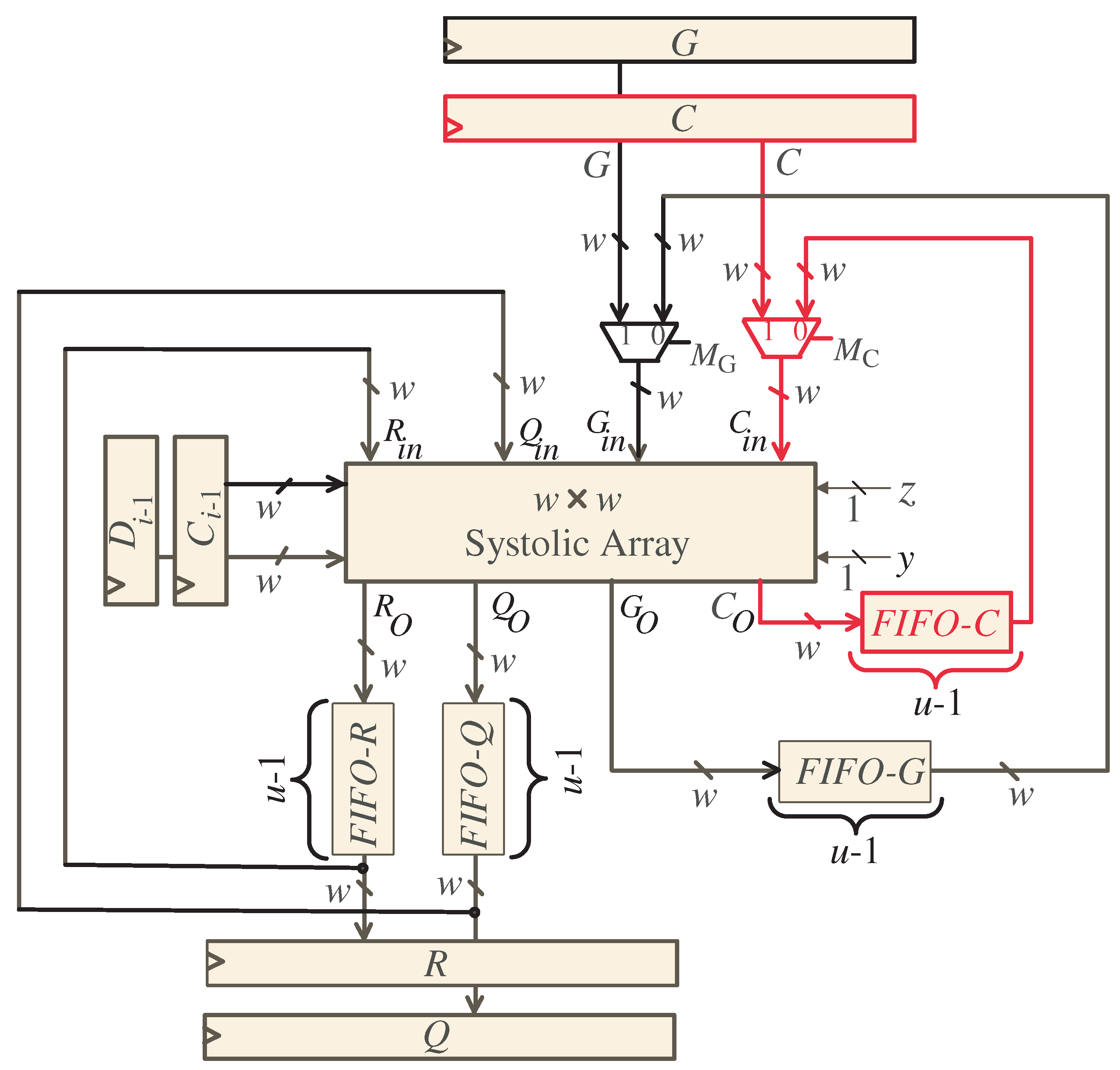
4. Combined Two-Dimensional SISO Multiplier-Squarer

A SISO combined multiplier-squarer requires feeding in polynomials C, D, and G in a word-serial fashion at the start of iterations and then obtaining the Q and R polynomials in a word-serial fashion. Let us assume that we would like to perform w iterations at the same time; i.e., we would like to feed in w bits of the polynomial inputs and obtain w bits of the partial results. There are several nonlinear task scheduling and projection functions that can be used to obtain different two-dimensional SISO combined multiplier-squarer. The most efficient ones are discussed in the following sections.

4.1. Two-Dimensional SISO Task Scheduling

Following the scheduling methodology explained in [33], we can extract the following nonlinear scheduling function to partition D into w × w equitemporal zones:
n ( p ) = m w i 1 w + m 1 j w + 1
where 1 i m + μ and μ j < m 1 .
Figure 2 shows the node timing (scheduling time) for the case when m = 5 and w = 2 .
Notice that we added an extra column on the right and extra row at the bottom to render the number of columns and rows integer multiples of w. In general, we should add μ extra columns and μ extra rows to render the number of columns and rows an integer multiple of w, where μ = w m w m .
Figure 3 shows the node timing (scheduling time) for the case when m = 5 , and w = 4 .
In this case μ = 3 , thus we had to add three extra columns on the right and three extra rows at the bottom to render the number of columns and rows an integer multiple of w. Therefore, the LSBs of inputs C and G and LSBs of the initial values of intermediate variables R and Q should be padded by μ zeros on the right as shown in Figure 3. Furthermore, the MSBs of inputs D and C should be padded by μ zeros at the bottom, as shown in the same figure.
The equitemporal zones are shown as light red boxes with the associated time index values indicated in red numerals within each zone. Notice that the bits of c m 1 i 1 are computed at the nodes of column m 2 , as shown in Figure 3 and broadcasted horizontally along with the bits of d i 1 and c i 1 to the nodes of row i 1 .
One last detail needs to be mentioned here and is best explained with reference to two adjacent equitemproal zones executing at times n and n + 1 . Figure 4 illustrates this situation.
The north and east inputs to zone i are available at times n and n + 1 , respectively. However, we notice that input C n only affects the west output C w and C e only affects the south output C s . Hence, at time n output C w is valid while output C s is not valid since we were required to add C e to it. This will result in an increase in the total number of iterations needed to produce the final result by one time step. Therefore, the total number of iterations needed to complete the combined multiplication/squaring computation will be provided by:
#   Iterations = m w 2 + 1

Two-Dimentional SISO Task Projection

Given the scheduling time in Figure 3, we note that only w × w nodes are active at a given time. Following the projection technique explained in [33], we can extract the following nonlinear projection function that maps a point p ( i , j ) D of Figure 3 to a point p ¯ in the PE space:
p ¯ ( o , l ) = P s i s o p ( i , j )
o = i mod w
l = j mod w
P s i s o = [ . mod w . mod w ]
where “dot” is a place holder for the argument.
Our systolic array will now consist of w 2 PEs arranged in w rows and w columns in addition to the necessary registers. Figure 5 shows the word-based two-dimensional SISO systolic processor.
The Word-based two-dimensional SISO systolic processor consists of w × w systolic array block as well as input/output registers and FIFO buffers in addition to two 2-input MUXes for selecting between the inputs of C and G and their intermediate values. The resulting intermediate words of R, Q, and C and the words of G are pipelined through the FIFO buffers of R, Q, C, and G, respectively. These FIFOs have a width size of w bits and a depth size of u 1 , where u = m w . The word update block ensures that the proper number of bits are extracted from the bottom outputs of the systolic array block shown in Figure 5. Notice that we added two registers for the input C: The north C register feeds the words of operand C to the systolic array starting from the most significant words, while the east register C i 1 feeds the words of operand C to the systolic array starting from the least significant words.
Figure 6 shows the details of the two-dimensional word-based SISO systolic array for the case when m = 5 and w = 4 . The PEs of the systolic array are divided into two different types with each type possessing a different color. The logical details of the PEs are shown in Figure 7 and Figure 8. The light blue PEs have an extra tri-state buffer that is enabled ( y = 0 ) at time steps n = k m w + 1 and 0 k < m w to pass the computed bits of C m 1 i 1 . These bits are broadcasted along with the input bits of D i 1 and C i 1 to the remaining nodes of the systolic array to compute the intermediate words of R, Q, and C. Moreover, they have an extra AND gate to enforce the partial results of the MSBs of C and c m i to be zero at the same time instances. This is controlled by the control signal y shown in Figure 7.
The operation of the two-dimensional SISO systolic processor can be summarized for the generic values of m and w as follows:
  • At time n = 1 , MUXes M C and M G shown in Figure 5, are set to pass the w MSBs of operands C and G, respectively, to the systolic array block. Moreover, FIFO buffers of R and Q are reset at the same time to pass zero inputs to the systolic array block since the initial values of R and Q are zeros as indicated in Algorithm 1. Notice that, the control signals y and z are set to 0 and 1, respectively, through this time step. The control signal y = 0 enables the tristate buffer shown in Figure 7 for all the light blue PEs of the systolic array, Figure 6, to pass the computed w bits of C m 1 i 1 and 1 i w . The computed word of C m 1 i 1 along with the w LSBs of D i 1 and C i 1 , 1 i w , are passed horizontally to the remaining PEs nodes of the systolic array. Moreover, the control signal y = 0 forces the bits of C m i and 1 i w through the AND gate shown in Figure 7 to have zero values as shown at the left edge of the DG, Figure 3.
  • At time instances 1 < n m w , MUXs M C and M G are still set to pass the remaining words of inputs C and G, one word at each time step, to the systolic array. These operand words are used with the horizontally passed words of C m 1 i 1 , D i 1 , and C i 1 , 1 i w , to compute the intermediate words of R, Q, and C in a word serial fashion. The resulting words of R, Q, and C are pipelined through the FIFOs of R, Q, and C shown in Figure 5, respectively. These FIFOs have a width size of w bits and a depth size of u 1 , where u = m w . Notice that the depth of R and Q FIFOs ensures keeping the initial values of R and Q equal to zero through these time instances.
  • At time instances n > m w , MUXs M C and M G passes the computed C words stored in FIFO-C and the G words stored in FIFO-G to the systolic array, one word at each time step. These words, along with the computed R and Q words that are stored in FIFO-R and FIFO-Q and the broadcasted words of C m 1 i 1 , D i 1 , and C i 1 , k w < i ( k + 1 ) w , 1 k m w 1 , are used to update the intermediate partial results of R, Q, and C in a word serial fashion, one word at each time step.
  • At time instances n = k m w + 1 , 0 k m w 1 the tri-sate buffer shown in Figure 7 is enabled ( y = 0 ) in all the light blue PEs of the systolic array, Figure 6, to pass horizontally through the computed w bits of C m 1 i 1 , k w < i ( k + 1 ) w , along with the w bits of inputs D i 1 and C i 1 , k w < i ( k + 1 ) w , to the remaining PEs nodes of the systolic array. Notice that the D i 1 and C i 1 registers, shown in Figure 5, feeds the systolic array with the input words of D i 1 and C i 1 through these time instances. Furthermore, through these time instances, the control signal ( y = 0 ) forces the bits of C m i and k w < i ( k + 1 ) w through the AND gate shown in Figure 7 to have zero values as shown at the left edge of the DG of Figure 3. At the remaining time instances, this control signal is equal to one.
  • Through time instances n = k m w + 1 , 1 k m w , the control signal z shown at the right side of Figure 6 is equal to zero to feed the zero values of C, shown at the right edge of DG of Figure 3, to the systolic array. At the remaining time instances, this control signal is equal to one.
  • Through time instances n m w m + μ 1 w , the resulting output words of R and Q will be loaded in a word serial fashion, one word at each time step, in registers R and Q shown in Figure 5, respectively.
An important note that should be considered here is that the vertical w bit words of R, Q, and G and the horizontal w bit words of C m 1 i 1 , D i 1 , and C i 1 are delayed one time step inside the systolic array as shown in Figure 6. This is represented by the D registers (squares) shown in this figure. This renders a one time step difference between the PEs above the D registers (squares) and the PEs below of them. This time difference is attributed to the intermediate words of C, resulting from the left column (blue cells) of the systolic array shown in Figure 6, that are produced starting from the second time step and the words of R, Q, G, C m 1 i 1 , D i 1 , and C i 1 should be delayed, as shown in Figure 6, to synchronize the operation. This resulted in the extra time step needed to complete the the combined multiplication/squaring computation as explained before in Equation (8).

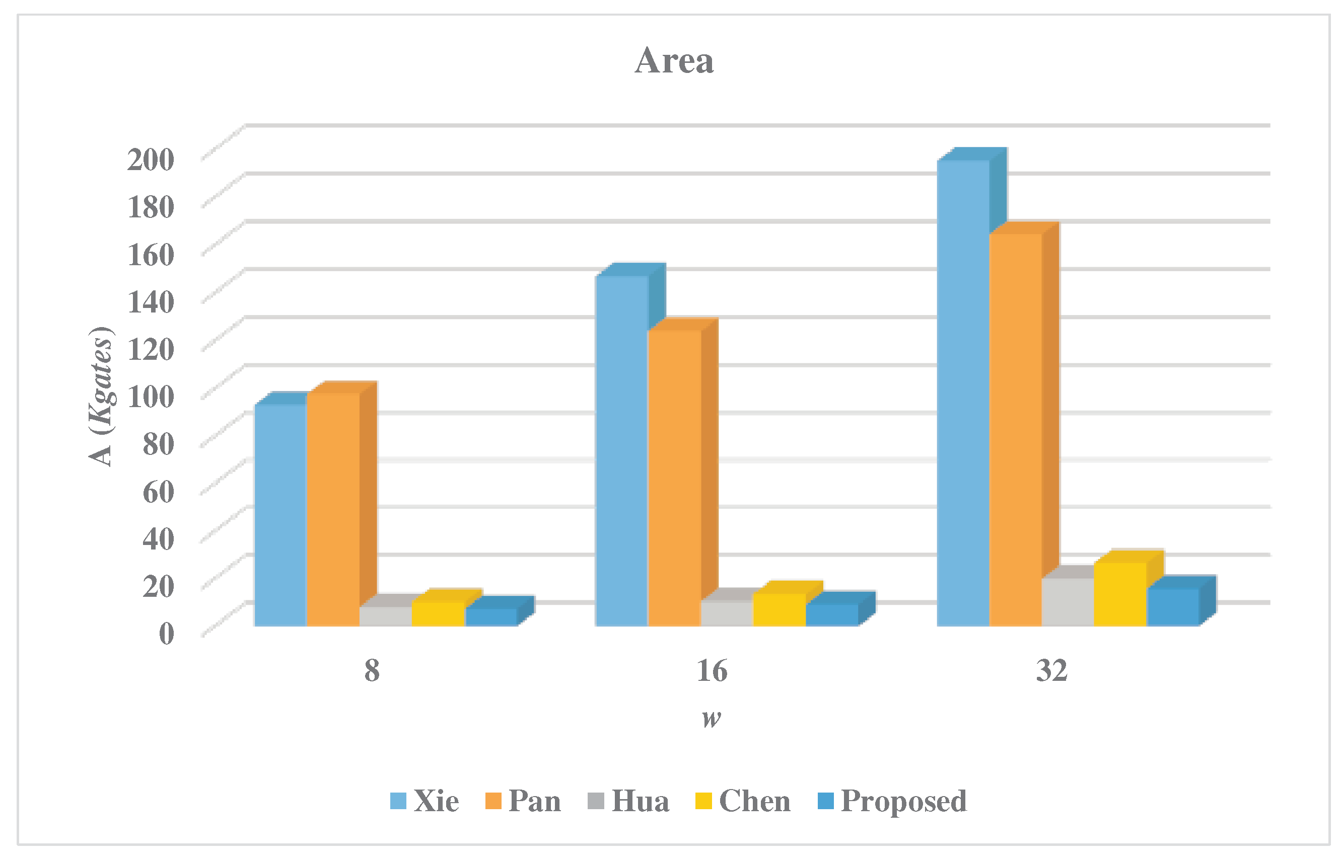
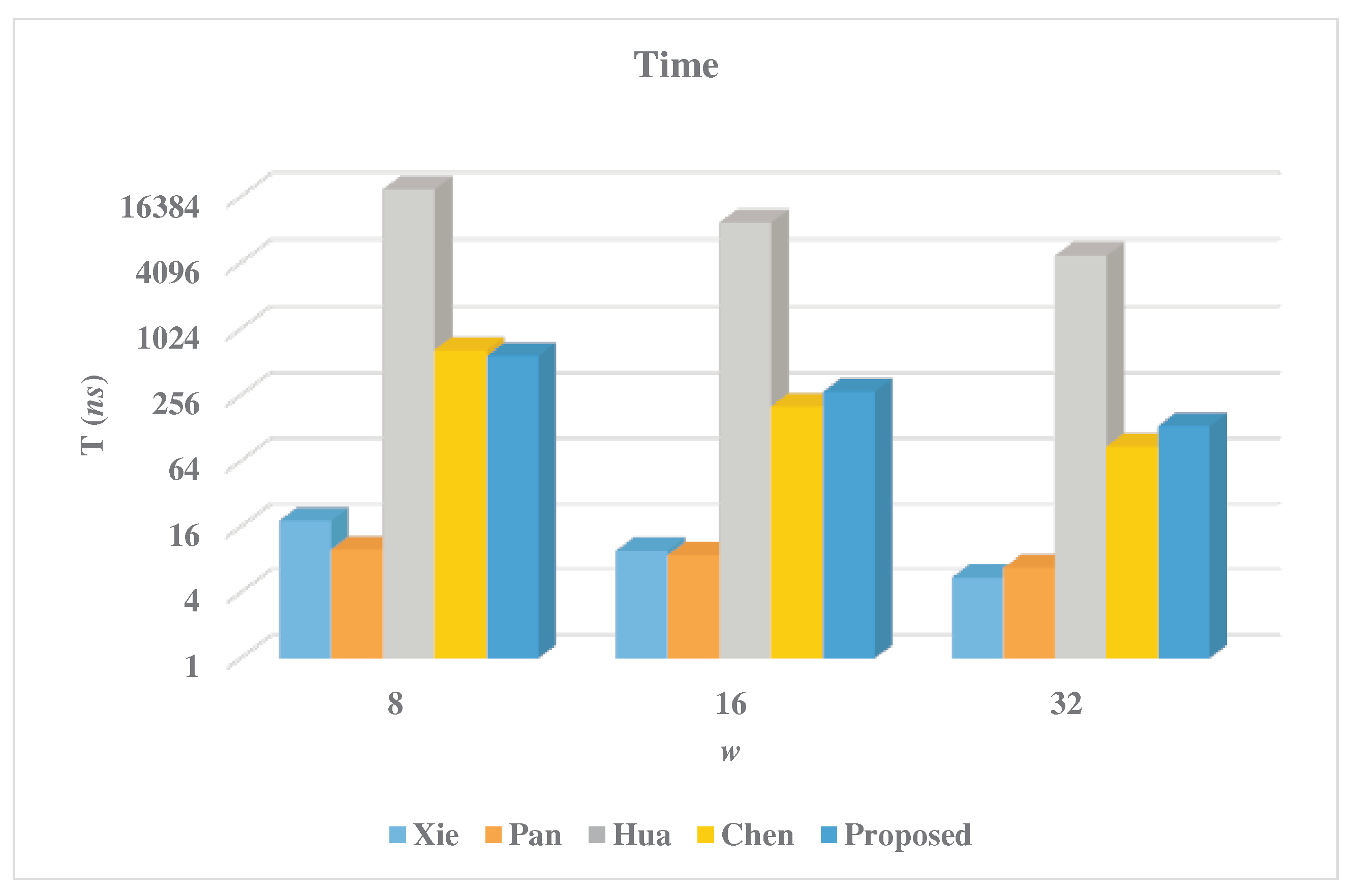
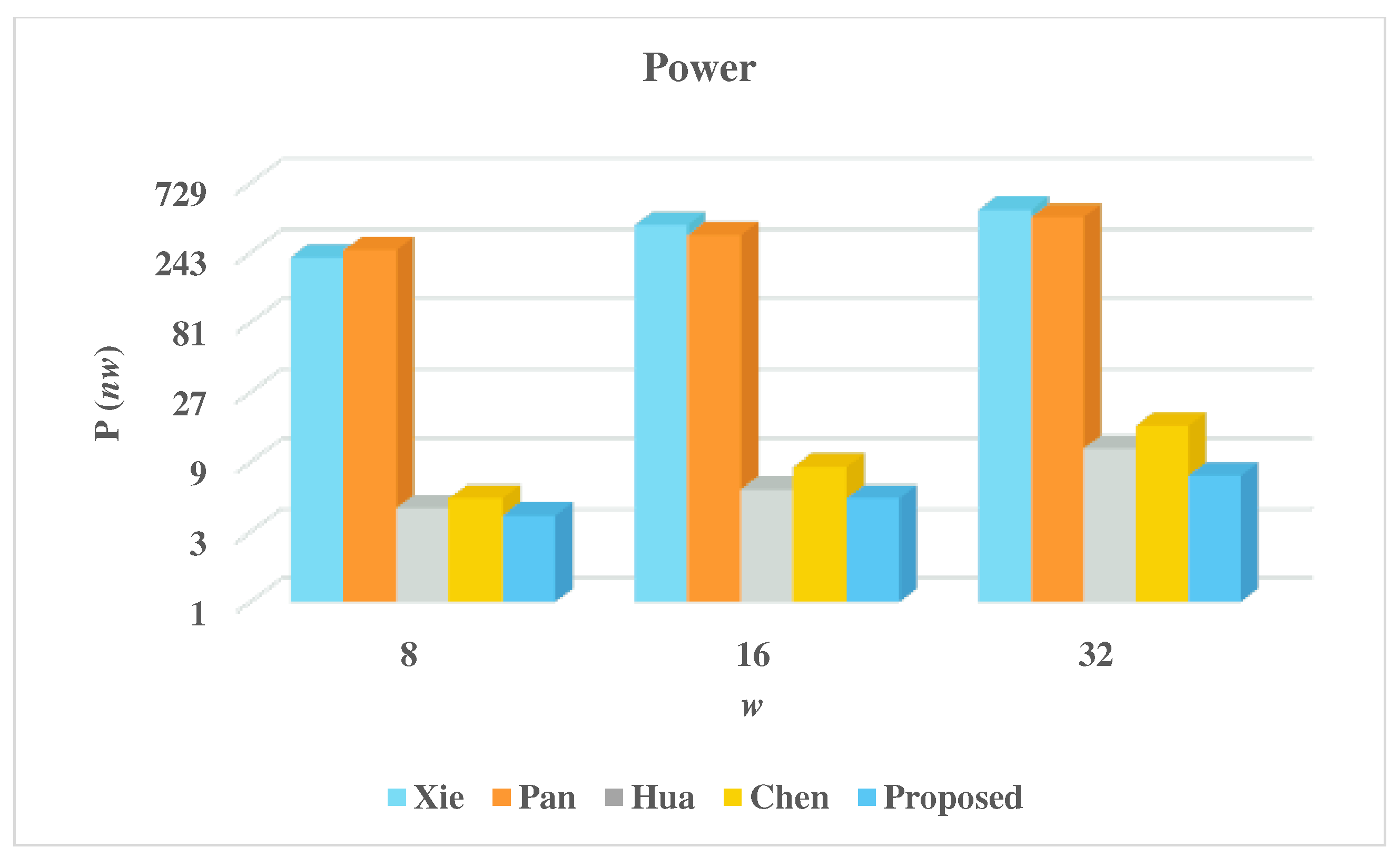
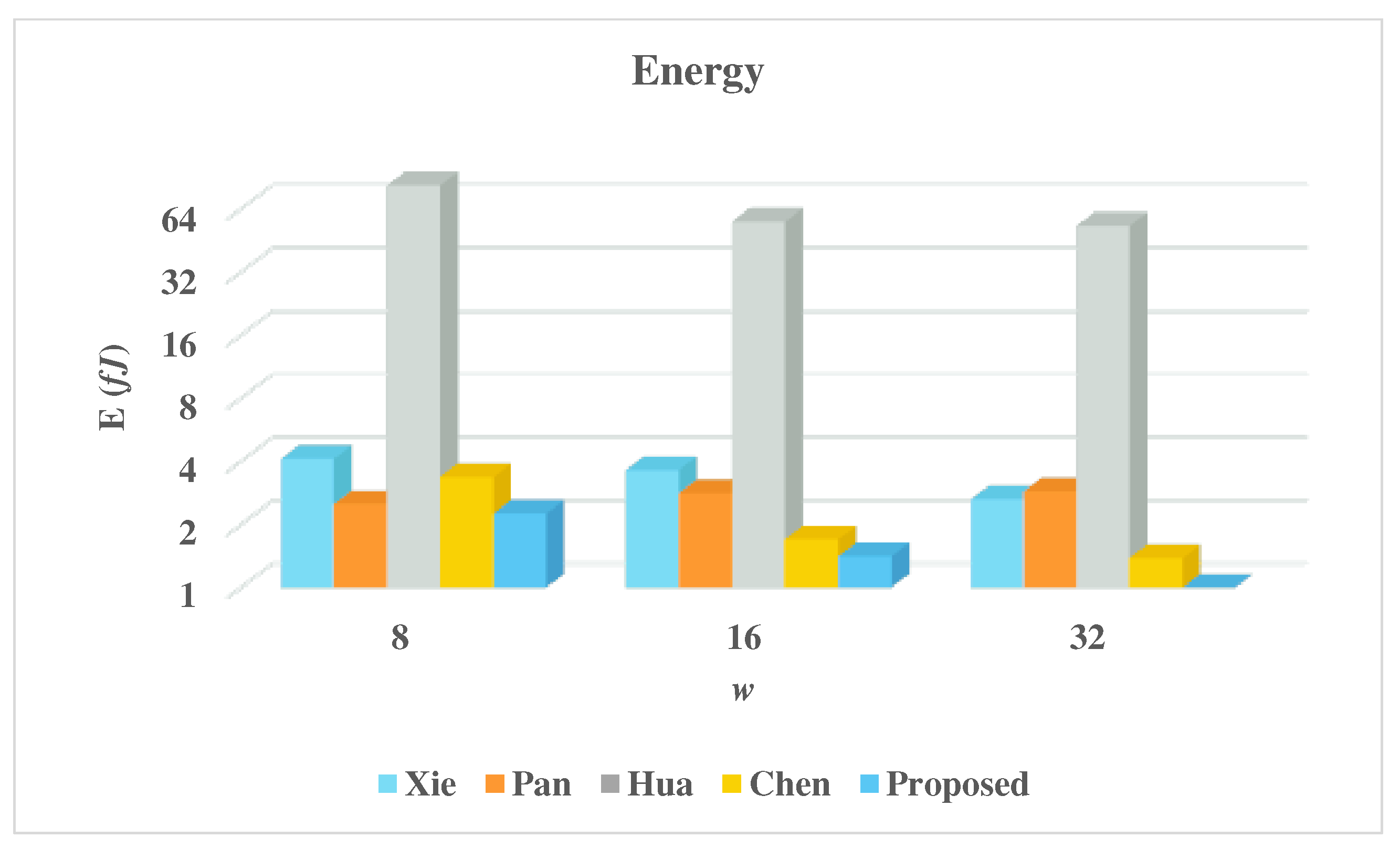
5. Experimental Results and Discussion

In this section, we compare the proposed two-dimensional word-serial combined multiplier-squarer structure and the best of the existing word-serial multiplier structures [18,23,40,41] in terms of area and time complexities. The area is estimated in terms of numbers of Tri-State buffers, 2-input AND gate, 2-input XOR gate, 2-input Multiplexers, and Flip-Flops. The time is represented by latency and Critical Path Delay (CPD).
The estimated area and time complexities of the compared structures are given in Table 1. In this Table, the field size and word size are represented by m and w, respectively. T A represents the delay of 2-input AND gate. T X represents the delay of 2-input XOR gate. T M U X represents the delay of 2-to-1 MUX. The notations F 1 , F 2 , F 3 , L 1 , τ 1 , τ 2 , τ 3 , and τ 4 are described by the following equations.
F 1 = 7 m + m ( log m ) + w + 3
F 1 represents the number of Flip-Flops in Pan et al. [18] design.
F 2 = 2 w 2 + 2 w ( m / w ) + 4 w + 1
F 2 represents the number of Flip-Flops in Hua et al. [40] design.
F 3 = 2 w 2 + 3 w ( m / w ) + 2 w
F 3 represents the number of Flip-Flops in Chen et al. [41] design.
L 1 = w + m / w 2 + m / w
L 1 represents the latency of Chen et al. [41] design.
τ 1 = T A + ( log 2 w + 1 ) T X
τ 1 represents the critical path delay of Pan et al. [18] design.
τ 2 = T A + 2 T X
τ 2 represents the critical path delay of Hua et al. [40] design.
τ 3 = T A + T X
τ 3 represents the critical path delay of Chen et al. [41] design.
τ 4 = ( w + 1 ) T A + w T X + T M U X
τ 4 represents the critical path delay of the proposed design.
For fair comparison, we added the area complexity of Input/Output registers for each design structure.
By inspecting Table 1, we observe that the expressions representing the estimated number of logic gates or components of the multiplier structures of Pan et al. [18] and Xie et al. [23] are approximate of order O ( m w ) . On the other hand, it is of order O ( w 2 ) for the other multiplier structures, except the MUXes and Flip-Flop components of the proposed design, which are of order O ( w 2 ) and O ( m / w ), respectively. Since m is extremely larger than w, we can conclude that the area complexity of the multiplier structures of Pan et al. [18] and Xie et al. [23] will be higher than that of all the other multiplier structures, including the suggested one. By examination of the gate counts’ expressions of the developed multiplier-squarer and multipliers of Hua et al. [40] and Chen et al. [41], we recognize that the proposed design has a lower number of Flip-Flops compared to them. The flip-flop area expression is of order O ( m / w ) for the suggested multiplier-squarer and it is of order O ( w 2 ) for the multipliers of Hua et al. [40] and Chen et al. [41]. Therefore, for large values of w, the number of flip-flops will be substantially decrease compared to the other multipliers. According to the standard CMOS libraries’ data, the Flip-Flop consumes the largest area on the chip compared to the other gate types. Thus, reducing the number of flip-flops in the design structure will considerably reduce the overall area, which accounts for the insignificant increase in the area of the proposed design as w increases. It is interesting to notice that the suggested design performs multiplication and squaring operations simultaneously and the compared ones perform both operations in sequence and, hence, reducing the area of the developed design for different word sizes can be considered a considerable achievement.
By examining the latency expressions in Table 1, we can conclude that the multiplier structure of Pan et al. [18] has lower latency and that the multiplier structure of Hua et al. [40] has the most significant latency compared to the remaining multiplier structures, including the recommended one. The numerical results displayed in Table 2 show that the proposed design has lower latency than the designs of Hua et al. [40] and Chen et al. [41] and higher latency than the multiplier designs of Xie et al. [23] and Pan et al. [18] for the common field size n = 409 . Furthermore, we can conclude from Table 1 that the latency of all multiplier structures typically decreases as word-size w increases as it is inversely proportional to w.
By analyzing the expressions of the CPD, for all word sizes of w, we can conclude that the multiplier structures of Xie et al. [23], Hua et al. [40], and Chen et al. [41] have a fixed and lower CPD. On the other hand, the CPD values of Pan et al. [18] and the developed design principally increases as w increases. We cannot accurately assume, from the estimated expressions, which design structure has the best execution time due to the difficulty in estimating the decreased amount of latency when w increases. The numerical results given in Table 2 will confirm the question of which multiplier structure presents better execution time complexity.
The designs in Table 1 are described using the VHDL code and synthesized for the common field size m = 409 and different values of w ( 8 , 16 , 32 ) to obtain real implementation results. We used the NanGate (15 nm, 0.8 V) Open Cell Library and Synopsys tools version 2005.09-SP2 for synthesizing. We used the typical corner ( V D D = 0.8 V and T j = 25 °C) and unit drive strength for all the utilized primitives.
Testing the proposed design starts by evaluating the wasted power at a frequency of 1 KHz for each multiplier structure. Then, through simulation using Mentor Graphics ModelSim SE 6.0a tools, we accumulated the switching activities in the Switching Activity Interchange Format (SAIF) file to obtain the power report. Next, we designed a testbench to simulate the suggested multiplier-squarer structure. The test bench has a single loop of 400 possible input combinations of 32-bits, each allowing the user to validate the correctness of the outputs. In order to regularly examine the resulting output’s correctness, we used an error flag to designate if the implemented design is working accurately or not. If the error flag sets to ’0’ at the end of the simulation, then the multiplier-squarer structure works perfectly. On the other hand, if it sets to ’1’, the multiplier-squarer design is not operating correctly. In order to allow the examiner to examine the generated output from each input set, we utilized a “wait statement” to produce a delay of 50 ns between test vectors. Furthermore, we performed a post-layout simulation to include the additional pin cost and the propagation delay of all gates. Accordingly, we can achieve an accurate evaluation of the area, time, and consumed power.
The obtained results are listed in Table 2. The design metrics used to compare the proposed and the existing word-serial designs can be defined as follows:
  • Latency: is the total number of clock cycles needed to complete a single operation;
  • Area (A): is the estimated design area in terms of the equivalent area of 2-input NAND gate;
  • CPD: is the synthesized critical path delay;
  • Time (T): is the total computation time required to complete a single operation;
  • Power (P): is the consumed power obtained at 1 KHZ;
  • Energy (E): is the consumed energy which obtained by multiplying power (P) by the total computation time (T).
For a fair comparison, the compared multiplier structures of [18,23,40,41] should perform multiplication and squaring operations in sequence and this doubles the obtained synthesis results of the time and consumed power/energy of these designs as indicated in Table 2. For a better explanation of the obtained results, we visualized area, time, power, and energy results by using the charts shown in Figure 9, Figure 10, Figure 11 and Figure 12, respectively.
Figure 9 indicates that the proposed design structure saves area at the different values of w by percentages ranging from 9.1% to 92.6% at w = 8 , 11.6% to 93.7% at w = 16 , and 20.7% to 91.9% at w = 32 over the existing designs. The design of Pan [18] saves 45.8% and 9.3% time at w = 8 and w = 16 , respectively, over the best of the other designs including the proposed one. The design of Xie [23] saves 18.4% time at w = 32 over the best of the other designs including the proposed one.
Figure 10 indicates that the multiplier of Pan [18] has the most reduced computation time at w = 8 over all the remaining designs, including the recommended one (at least 40% lower time than the multiplier of Xie [23]). At w = 16 and w = 32 , the multiplier of Xie [23] has the cheapest computation time over the remaining designs (at least reduction by 0.6% at w = 16 and 6.5% at w = 32 over the multiplier of Pan [18]). The multiplier of Xie [23] outperforms the remaining designs at w = 16 and w = 32 due to the significant reduction in its latency compared to the other multiplier designs.
Figure 11 indicates the developed design that has the lowest power consumption at all word sizes due to its significant reduction in area. The savings in the area will reduce the parasitic capacitance and, thus, reduces the switching activities in the entire circuit, which is one of the main contributors to power consumption. We noticed from Table 2 that the proposed design reduces power consumption at different word sizes by percentages ranging from 10.8% to 98.5% at w = 8 , 12.5% to 98.4% at w = 16 , and 34.7% to 98.5% at w = 32 over the existing designs.
Figure 12 indicates that the proposed design structure has the a significant reduction in energy over all the remaining multipliers at the different values of w. By observing the energy results in Table 2, we notice that the proposed design saves energy at the different values of w by percentages ranging from 9.6% to 97.3% at w = 8 , 17.1% to 97.5% at w = 16 , and 29.0% to 98.2% at w = 32 over the existing designs. The reduction in consumed energy of the proposed design, at all word sizes, is mainly attributed to the fair values of its execution time (T) and the lower values of the consumed power.
As we notice, the proposed design has the lower area, power, and consumed energy at all of the embedded word sizes. Thus, it enables the implementation of cryptographic processors in resource-constrained IoT edge devices such as hand-held devices, wearable and implantable medical devices, wireless sensor nodes, smart cards, and radio frequency identification (RFID) devices.

6. Summary and Conclusions

This paper presented new efficient two-dimensional word-based SISO systolic processor for performing the multiplication and squaring operations concurrently over G F ( 2 m ) . The proposed systolic processor structure shares the data-path and this results in saving more area and power resources. We applied non-linear scheduling and projection functions to the algorithm dependency graph to explore the proposed systolic processor core. The applied non-linear scheduling and projection functions provide the designer more flexibility to control the processor work load and the execution time. The size of the systolic array in the processor core does not depend on the field size and that renders the proposed design more suitable for implementation in embedded and ultra-low power devices. Implementation results of the proposed two-dimensional combined word-serial processor systolic structure and the best of the existing word-serial multiplication designs show that the proposed structure achieves significant savings in area and consumed energy at different values of the embedded word sizes. This renders it more suitable for constrained implementations of cryptographic primitives in resource-constrained IoT edge devices such as hand-held devices, wearable and implantable medical devices, wireless sensor nodes, smart cards, and radio frequency identification (RFID) devices.

Author Contributions

Conceptualization, A.I. and F.G.; methodology, A.I. and F.G.; software, A.I.; validation, A.I. and F.G.; formal analysis, A.I.; investigation, A.I.; resources, A.I.; data curation, A.I.; writing—original draft preparation, A.I.; writing—review and editing, A.I. and F.G.; visualization, A.I. and F.G.; supervision, A.I.; project administration, A.I. and F.G.; funding acquisition, F.G. All authors have read and agreed to the published version of the manuscript.

Funding

This research was funded by the NATIONAL RESEARCH COUNCIL OF CANADA (NRC) grant number 51291-52200.

Acknowledgments

The authors would like to acknowledge the financial support of the National Research Council of Canada (NRC) grant under the Collaborative R&D Initiative.

Conflicts of Interest

The authors declare no conflict of interest.

Abbreviations

The following abbreviations are used in this manuscript:
IoTInternet of Things;
RFIDRadio Frequency Identification;
ASICApplication Specific Integrated Circuit;
RSARivest, Shamir, and Adleman;
DSADigital Signature Algorithm;
ECCElliptic Curve Cryptography;
SISOSerial-In/Serial-Out;
SIPOSerial-In/Parallel-Out;
PISOParallel-In/Serial-Out;
RIARegular Iterative Algorithm;
CPDCritical Path Delay.

References

  1. Chen, D.; Zhang, N.; Qin, Z.; Mao, X.; Qin, Z.; Shen, X.; Li, X.Y. S2M: A lightweight acoustic fingerprints-based wireless device authentication protocol. IEEE Internet Things J. 2016, 4, 88–100. [Google Scholar] [CrossRef]
  2. Sowjanya, K.; Dasgupta, M.; Ray, S. An elliptic curve cryptography based enhanced anonymous authentication protocol for wearable health monitoring systems. Int. J. Inf. Secur. 2020, 19, 129–146. [Google Scholar] [CrossRef]
  3. Granjal, J.; Monteiro, E.; Silva, J.S. Security for the internet of things: A survey of existing protocols and open research issues. IEEE Commun. Surv. Tutor. 2015, 17, 1294–1312. [Google Scholar] [CrossRef]
  4. Safkhani, M.; Vasilakos, A. A new secure authentication protocol for telecare medicine information system and smart campus. IEEE Access 2019, 7, 23514–23526. [Google Scholar] [CrossRef]
  5. Aghili, S.F.; Mala, H.; Kaliyar, P.; Conti, M. Seclap: Secure and lightweight RFID authentication protocol for medical IoT. Future Gener. Comput. Syst. 2019, 101, 621–634. [Google Scholar] [CrossRef]
  6. Anajemba, J.H.; Iwendi, C.; Mittal, M.; Yue, T. Improved advance encryption standard with a privacy database structure for IoT nodes. In Proceedings of the 2020 IEEE 9th International Conference on Communication Systems and Network Technologies (CSNT), Gwalior, India, 10–12 April 2020; pp. 201–206. [Google Scholar]
  7. Anajemba, J.H.; Yue, T.; Iwendi, C.; Alenezi, M.; Mittal, M. Optimal cooperative offloading scheme for energy efficient multi-access edge computation. IEEE Access 2020, 8, 53931–53941. [Google Scholar] [CrossRef]
  8. Atzori, L.; Iera, A.; Morabito, G. The internet of things: A survey. Comput. Netw. 2010, 54, 2787–2805. [Google Scholar] [CrossRef]
  9. Rivest, R.L.; Shamir, A.; Adleman, L. A method for obtaining digital signatures and public-key cryptosystems. Mag. Commun. ACM 1978, 21, 120–126. [Google Scholar] [CrossRef]
  10. Lidl, R.; Niederreiter, H. Introduction to Finite Fields and Their Applications; Cambridge University Press: Cambridge, UK, 1994. [Google Scholar]
  11. Chiou, C.W.; Lee, C.Y.; Deng, A.W.; Lin, J.M. Concurrent error detection in Montgomery multiplication over GF(2m). IEICE Trans. Fundam. Electron. Commun. Comput. Sci. 2006, E89-A, 566–574. [Google Scholar] [CrossRef]
  12. Kim, K.W.; Jeon, J.C. Polynomial Basis Multiplier Using Cellular Systolic Architecture. IETE J. Res. 2014, 60, 194–199. [Google Scholar] [CrossRef]
  13. Choi, S.; Lee, K. Efficient ssystolic modular multiplier/squarer for fast exponentiation over GF(2m). IEICE Electron. Express 2015, 12, 1–6. [Google Scholar] [CrossRef] [Green Version]
  14. Kim, K.W.; Kim, S.H. Efficient bit-parallel systolic architecture for multiplication and squaring over GF(2m). IEICE Electron. Express 2018, 15, 1–6. [Google Scholar] [CrossRef] [Green Version]
  15. Kim, C.H.; Hong, C.P.; Kwon, S. A digit-serial multiplier for finite Field GF(2m). IEEE Trans. Very Large Scale Integr. (VLSI) Syst. 2005, 13, 476–483. [Google Scholar]
  16. Talapatra, S.; Rahaman, H.; Mathew, J. Low complexity digit serial systolic montgomery multipliers for special class of GF(2m). IEEE Trans. Very Large Scale Integr. (VLSI) Syst. 2010, 18, 847–852. [Google Scholar] [CrossRef]
  17. Guo, J.H.; Wang, C.L. Hardware-efficient Systolic Architecture for Inversion and Division in GF(2m). IEE Proc. Comput. Digit. Tech. 1998, 145, 272–278. [Google Scholar] [CrossRef]
  18. Pan, J.S.; Lee, C.Y.; Meher, P.K. Low-Latency Digit-Serial and Digit-Parallel Systolic Multipliers for Large Binary Extension Fields. IEEE Trans. Circ. Syst.-I 2013, 60, 3195–3204. [Google Scholar] [CrossRef]
  19. Lee, C.Y.; Fan, C.C.; Yuan, S.M. New Digit-Serial Three-Operand Multiplier over Binary Extension Fields for High-Performance Applications. In Proceedings of the 2017 2nd IEEE International Conference on Computational Intelligence and Applications, Beijing, China, 8–11 September 2017; pp. 498–502. [Google Scholar]
  20. Hariri, A.; Reyhani-Masoleh, A. Digit-serial structures for the shifted polynomial basis multiplication over binary extension fields. In Proc. LNCS Intl Workshop Arithmetic of Finite Fields (WAIFI); Springer: Berlin/Heidelberg, Germany, 2008; pp. 103–116. [Google Scholar]
  21. Kumar, S.; Wollinger, T.; Paar, C. Optimum digit serial multipliers for curve-based cryptography. IEEE Trans. Comput. 2006, 55, 1306–1311. [Google Scholar] [CrossRef]
  22. Lee, C.Y. Super digit-serial systolic multiplier over GF(2m). In Proceedings of the 6th International Conference Genetic Evolutionary Computing, Kitakyushu, Japan, 25–28 August 2012; pp. 509–513. [Google Scholar]
  23. Xie, J.; Meher, P.K.; Mao, Z. Low-latency high-throughput systolic multipliers over GF(2m) for NIST recommended pentanomials. IEEE Trans. Circuits Syst. 2015, 62, 881–890. [Google Scholar] [CrossRef]
  24. Namin, A.H.; Wu, H.; Ahmadi, M. A word-level finite field multiplier using normal basis. IEEE Trans. Comput. 2011, 60, 890–895. [Google Scholar] [CrossRef]
  25. Lee, C.Y.; Chiou, C.W.; Lin, J.M.; Chang, C.C. Scalable and systolic Montgomery multiplier over generated by trinomials. IET Circuits Devices Syst. 2007, 1, 477–484. [Google Scholar] [CrossRef]
  26. Chen, L.H.; Chang, P.L.; Lee, C.Y.; Yang, Y.K. Scalable and systolic dual basis multiplier Over GF(2m). Int. J. Innov. Comput. Inf. Control 2011, 7, 1193–1208. [Google Scholar]
  27. Orlando, G.; Paar, C. A super-serial galois fields multiplier for FPGAs and its application to public-key algorithms. In Proceedings of the IEEE Symposium Field-Programmable Custom Computing, Napa Valley, CA, USA, 23 April 1999; pp. 232–239. [Google Scholar]
  28. Bayat-Sarmadi, S.; Kermani, M.M.; Azarderakhsh, R.; Lee, C.Y. Dual Basis Super-Serial Mult. for Secure Applications and Lightweight Cryptographic Arch. IEEE Trans. Circ. Syst.-II 2014, 61, 125–129. [Google Scholar]
  29. Gebali, F.; Ibrahim, A. Efficient Scalable Serial Multiplier Over GF(2m) Based on Trinomial. IEEE Trans. Very Large Scale Integr. (VLSI) Syst. 2015, 23, 2322–2326. [Google Scholar] [CrossRef]
  30. Ibrahim, A.; Gebali, F.; El-Simary, H.; Nassar, A. High-performance, low-power architecture for scalable radix 2 Montgomery modular multiplication algorithm. IEEE Can. J. Electr. Comput. Eng. 2009, 34, 152–157. [Google Scholar] [CrossRef]
  31. Ibrahim, A.; Gebali, F. Scalable and Unified Digit-Serial Processor Array Architecture for Multiplication and Inversion over GF(2m). IEEE Trans. Circuits Syst. I Regul. Pap. 2017, 22, 2894–2906. [Google Scholar] [CrossRef]
  32. Kim, K.W.; Lee, J.D. Efficient unified semi-systolic arrays for multiplication and squaring over GF(2m). IEICE Electron. Express 2017, 14, 1–10. [Google Scholar] [CrossRef] [Green Version]
  33. Gebali, F. Algorithms and Parallel Computers; John Wiley: New York, NY, USA, 2011. [Google Scholar]
  34. Ibrahim, A.; Elsimary, H.; Gebali, F. New systolic array architecture for finite field division. IEICE Electronics Express 2018, 15, 1–11. [Google Scholar] [CrossRef] [Green Version]
  35. Ibrahim, A.; Elsimary, H.; Aljumah, A.; Gebali, F. Reconfigurable hardware accelerator for profile hidden Markov models. Arabian J. Sci. Eng. 2016, 41, 3267–3277. [Google Scholar] [CrossRef]
  36. Ibrahim, A. Scalable digit-serial processor array architecture for finite field division. Microelectron. J. 2019, 85, 83–91. [Google Scholar] [CrossRef]
  37. Ibrahim, A.; Alsomani, T.; Gebali, F. Unified Systolic Array Architecture for Field Multiplication and Inversion Over GF(2m). Comput. Electr. Eng. J.-Elsevier 2017, 61, 104–115. [Google Scholar] [CrossRef]
  38. Ibrahim, A.; Alsomani, T.; Gebali, F. New Systolic Array Architecture for Finite Field Inversion. IEEE Can. J. Electr. Comput. Eng. 2017, 40, 23–30. [Google Scholar]
  39. Gebali, F.; Ibrahim, A. Low space-complexity and low power semi-systolic multiplier architectures over GF(2m) based on irreducible trinomial. Microprocess. Microsyst. 2016, 40, 45–52. [Google Scholar] [CrossRef]
  40. Hua, Y.Y.; Lin, J.M.; Chiou, C.W.; Lee, C.Y.; Liu, Y.H. Low space-complexity digit-serial dual basis systolic multiplier over Galois field GF (2m) using Hankel matrix and Karatsuba algorithm. IET Inf. Secur. 2013, 7, 75–86. [Google Scholar]
  41. Chen, C.C.; Lee, C.Y.; Lu, E.H. Scalable and Systolic Montgomery Multipliers Over GF(2m). IEICE Trans. Fundam. Electron. Commun. Comput. Sci. 2008, E91-A, 1763–1771. [Google Scholar] [CrossRef]
Figure 1. Dependence graph for the combined multiplication-squaring algorithm for m = 5 .
Electronics 10 01777 g001
Figure 2. Scheduling time for the case when m = 5 and w = 2 .
Electronics 10 01777 g002
Figure 3. Scheduling time for the case when m = 5 and w = 4 .
Electronics 10 01777 g003
Figure 4. Data dependencies of two adjacent equitemporal zones from Figure 3.
Electronics 10 01777 g004
Figure 5. Word-based two-dimensional SISO systolic processor.
Electronics 10 01777 g005
Figure 6. Word-based two-dimensional SISO systolic array.
Electronics 10 01777 g006
Figure 7. Light blue PE details of SISO two-dimensional systolic array.
Electronics 10 01777 g007
Figure 8. Light Orange PE details of SISO two-dimensional systolic array.
Electronics 10 01777 g008
Figure 9. Comparison of area results.
Electronics 10 01777 g009
Figure 10. Comparison of time results.
Electronics 10 01777 g010
Figure 11. Comparison of consumed power results.
Electronics 10 01777 g011
Figure 12. Comparison of consumed energy results.
Electronics 10 01777 g012
Table 1. Comparison between different word-serial field multipliers.
DesignTri-StateANDXORMUXsFlip-FlopsLatencyCPD
Xie [23]0 2 m w 2 m w + 6 m 6 m w + 6 0 4 m w + 4 m + 2 w 2 m / w + 2 log 2 w 2 T X
Pan [18]0 m m m w ( 2 + m ) + w 0 F 1 2 m / w τ 1
Hua [40]0 w 2 w 2 + 4 5 w + 1 ( 1 ) 0 F 2 6 w m / w 2 τ 2
Chen [41]0 w 2 + w w 2 + 2 w 2 w ( 2 ) F 3 L 1 τ 3
Proposedw 3 w 2 + 2 w 3 w 2 2 w 4 w ( m / w + 1 ) m / w 2 + 1 τ 4
(1) Area of 3-input XOR gate as 1.5 × a 2-input XOR gate. (2) Multiplier of [41] uses switches that having same transistor count as 2-input MUX.
Table 2. Implementation results of different word-serial field multipliers for m = 409 and different values of w.
MultiplierwLatencyArea (A)CPDTime (T)Power (P)Energy (E)
(Kgates)(ps)(ns)(nW)(fJ)
Xie [23]832492.9856.418.27225.564.12
16172146.9656.49.70375.53.64
3298195.1356.45.53477.42.64
Pan [18]84897.46206.39.90252.912.50
1636123.93244.48.80320.072.82
3224164.34282.56.78425.092.88
Hua [40]8259,5847.9973.419053.474.3582.88
16129,79210.4073.49526.735.8555.73
326489619.9173.44763.3711.1553.11
Chen [41]81194610.1655.2659.425.113.37
16367813.5155.2203.038.381.70
32157226.5855.286.7715.951.38
Proposed827057.26215.7583.473.882.26
166779.19407.7276.015.121.41
3217015.78791.7134.597.280.98
Publisher’s Note: MDPI stays neutral with regard to jurisdictional claims in published maps and institutional affiliations.

