
Characterization Techniques of Millimeter-Wave Orthomode Transducers (OMTs)


1
INAF (National Institute for Astrophysics), Astronomical Observatory of Cagliari, 09047 Selargius, Italy
2
INAF (National Institute for Astrophysics), Astrophysical Observatory of Arcetri, 50125 Firenze, Italy
*
Author to whom correspondence should be addressed.
Electronics 2021, 10(15), 1844; https://0-doi-org.brum.beds.ac.uk/10.3390/electronics10151844
Submission received: 14 June 2021
/
Revised: 28 July 2021
/
Accepted: 28 July 2021
/
Published: 31 July 2021
(This article belongs to the Section Microwave and Wireless Communications)
Abstract
:We report on advanced techniques for the accurate characterization of millimeter-wave Orthomode Transducers (OMTs) enabling the derivation of the fundamental parameters of such devices, i.e., the insertion loss, the return loss, the cross-polarization, and the isolation. These techniques include standard frequency-domain and time-domain VNA (Vector Network Analyzer) measurement methods, which can be applied to remove the effects of the waveguide transitions necessary to access the OMT ports and excite the desired modes. After reviewing the definition of the OMT parameters, we discuss the test equipment, the VNA calibration procedures as well as the VNA time-domain time-gating method for application in OMT characterization. We present simplified equations that relate the calibrated VNA measured quantities with the OMT S-parameters, illustrate various characterization methods, and examine various OMT experimental test setups. The advantages and disadvantages of each of the OMT characterization procedures are presented and compared among them. We provide a list of waveguide components required in the OMT test setups (adapters, loads, quarter-wave and longer waveguide sections, feed-horn, etc.), discuss the error terms introduced by such components and examine their impact on the measured values. Furthermore, we identify strategies to mitigate or remove the effects of the measured errors, to derive the desired OMT parameters. Different OMT configurations, with a distinct orientation of the waveguide input and outputs, are discussed. Although the presented techniques refer to the characterization of a specific configuration of a W-band OMT, the described methods can be applied to other OMT configurations and frequency ranges (from microwave to THz frequencies), therefore having a general validity.
1. Introduction
An Orthomode Transducer (OMT) is a passive device operating in a dual mode [1]: in receiver mode, it separates two orthogonal linearly polarized signals at its common input port to two independent physical ports at its output; in transmitter mode, it combines two independent signals at its two input ports into two separate polarizations at the common output port. In the two operating modes, input/output port/ports are exchanged. Here, we focus on the receiver mode, being most of the discussion valid also in transmitting mode. The polarization separation is obtained over a given frequency range. An OMT has three physical ports, but exhibits properties of a four-port device, because the input common port, usually a waveguide with a square or circular cross-section, provides two electrical ports that correspond to the two independent orthogonal polarized signals. Various OMT types exist, based on broadband symmetric structures. A full selection of references that describe OMTs operating at millimeter and submillimeter wavelengths are given in [2,3,4,5,6,7,8,9,10,11,12,13,14,15,16,17,18,19,20,21,22,23,24]. Symmetric designs include the Bøifot junction [2,3,4,5,6], the turnstile junction [7,8,9,10,11], the double-ridge junction [12,13,14,15], the symmetric reverse-coupler junction [16,17,18,19] the finline design [20], the planar design [21] and the design with balanced coaxial probe [22]. Example of simple asymmetric structures that can achieve good performance over narrower bandwidths are given in [23,24].
In the above-cited references, design aspects are of prime importance and experimental characterization is presented to prove the validity of the design process, without extensive discussion of the adopted measurement technique. This paper aims to focus on the measurement techniques themselves as found in the literature in many OMT-related works, the already referenced ones, as well as many others not cited here. To our knowledge, very few specific articles addressing OMT measurement techniques can be found in the literature: we can cite for example [25], where a specific procedure and theoretical analysis for the full experimental characterization of OMTs is discussed, which is based on the elaboration of five measurements at a single polarized port.
Here, we extend the analysis of OMT characterization techniques to include more general less-specific procedures. We describe most of the OMT characterization techniques that can be used in practice, and focus on applications in the millimeter-wave spectral range.
The schematic diagram of an OMT as a four-electrical-port device is shown in Figure 1. Electrical Ports 1 and 2 are associated with the two orthogonally incident polarization signals at the input of the device. They share the same physical port. Port 1 signal is defined here as the “Vertical Polarization” and is represented by a vertical E-field vector VP, while Port 2 signal is defined as the “Horizontal Polarization” and is represented by a horizontal E-field vector HP.
2. Ideal OMT and Definition of OMT Parameters
In an ideal OMT, the VP signal at Port 1 is fully coupled to the VP output port, Port 3, while the HP signal at Port 2 is fully coupled to the HP output port, Port 4. In addition, the VP and HP signals at the common ports, Port 1 and Port 2, are perfectly matched (no reflection). All other port couplings are ideally null. The S-parameter matrix [26,27,28] of a generic four-port device is given in Equation (1), while the one of an ideal OMT is given in Equation (2):
In general, the elements Sij of the matrix have frequency-dependent complex values that represent the complex fraction of the unit amplitude wave incident at port j that exits from port i, while their absolute square values represent the associated fraction of power. The S-matrix of an ideal OMT is given in Equation (2), where the amplitudes of elements S31, S42, S13, and S24 are unitary (on a linear scale) and the only ones being non-null. The phases of the non-null Sij are also indicated (θ31, θ42, θ13, and θ24). A Vector Network Analyzer (VNA) measures the scattering matrix elements of a network and can be used to derive the elements Sij of an OMT i.e., the amplitude and phase of voltage traveling wave phasors at the OMT ports.
An OMT is a passive device commonly made of reciprocal materials and therefore has properties of a reciprocal network. A reciprocal network is one in which the transmission of a signal between any two ports does not depend on the direction of propagation, i.e., input and output ports are interchangeable. In S-parameter terms, reciprocity entails scattering matrix symmetry, i.e., Sij = Sji for any i ≠ j, i.e., S12 = S21, S13 = S31, etc. (here we note that most passive networks such as cables, attenuators, power dividers, and couplers are reciprocal and that the only case where a passive device is not reciprocal is when it contains anisotropic materials, such as ferrite used in circulators and isolators). In particular, for an ideal OMT we have θ31 = θ13, θ42 = θ24.
The main parameters that characterize the performance of an OMT are the following:
- The Insertion Loss, IL, of the two polarization channels;
- The Input Return Loss, IRL, of the two polarizations at the common port;
- The Output Return Loss, ORL, of the two single polarization waveguide outputs;
- The Cross-Polarization, XP, between an input and an output port associated with different polarization channels;
- The Isolation, ISO, between the two output ports.
The two insertion losses, ILs, are associated with the signal losses through the OMT from Port 1 to the corresponding output Port 3 (IL31), and from Port 2 to the corresponding Port 4 (IL42); they are defined in Equations (3) and (4) as follows:
In the ideal OMT, the IL = 0 dB (unitary, in linear scale) for both orthogonal polarization channels (IL31 = IL42 = 0 dB), i.e., the device is lossless. Please note that by definition (see for example [26,27,28]) the insertion loss of a passive device is a non-negative number (always ≥0 dB), unlike the transmission coefficient that has the opposite sign to it and is always non-positive (≤0 dB). Therefore, the sign of the insertion loss is opposite to the amplitude of the transmission coefficient when expressed in dB.
By definition, the insertion loss IL31, associated with the transmission from Port 1 to Port 3, is to be measured with all other ports (Port 2 and Port 4) terminated with a matched load. Similarly, the insertion loss IL42, associated with the transmission from Port 2 to Port 4, is to be measured with all other ports (Port 1 and Port 3) terminated with a matched load. As common OMTs are passive reciprocal networks, we have IL31 = IL13 (S31 = S13) and IL42 = IL24 (S42 = S24), where IL13 = −20log10|S13| and IL24 = −20log10|S24|.
The Input Return Loss of the OMT, IRL, is associated with the ratio between the reflected and the incident wave amplitudes at the input of the device. Input Return Loss is defined separately for each electrical input, i.e., for VP (|S11|) and HP (|S22|), as in Equations (5) and (6):
In the ideal OMT, the IRL is infinite when expressed in dB for both orthogonal polarization channels (IRL11 = IRL22 = ∞ dB). By definition, the return loss is a non-negative number (always ≥0 dB), unlike the reflection coefficient, which has the opposite sign to it and is always non-positive (≤0 dB). Therefore, the sign of the return loss is opposite to the amplitude of the reflection coefficient when expressed in dB.
By definition, the input return loss IRL11, associated with the reflection from Port 1, is to be measured with all other ports (Port 2, Port 3, and Port 4) terminated with a matched load. Similarly, the input return loss IRL22, associated with the reflection from Port 2, is to be measured with all other ports (Port 1, Port 3, and Port 4) terminated with a matched load.
The Output Return Loss of the OMT, ORL, is associated with the ratio between the reflected and the incident wave amplitudes at the output of the device and defined in Equations (7) and (8) as follows:
In the ideal OMT, the ORL is infinite when expressed in dB for both orthogonal polarization channels (ORL33 = ORL44 = ∞ dB). By definition, the output return loss ORL33, associated with the reflection from Port 3, is to be measured with all other ports (Port 1, Port 2, and Port 4) terminated with a matched load. Similarly, the output return loss ORL44, associated with the reflection from Port 4, is to be measured with all other ports (Port 1, Port 2, and Port 3) terminated with a matched load.
The OMT cross-polarization, XP, referred also to as “Crosstalk” or “Polarization Isolation,” represents the ability of the OMT to keep uncoupled the two polarization channels, avoiding any energy leakage from one channel to the other. It is measured from the input port to the uncoupled output port, thus being associated with the two scattering parameters S41 and S32. The cross-polarization is associated with the signal transmission to the unwanted output port and defined in Equations (9) and (10) as:
In the ideal OMT, the XP is infinite when expressed in dB for both orthogonal polarization channels (XP41 = XP32 = ∞ dB). By definition, the cross-polarization XP41 associated with the transmission between Port 1 and Port 4 is to be measured with Port 2 and Port 3 terminated into a matched load. Similarly, the cross-polarization XP32 associated with the transmission between Port 3 and Port 2 is to be measured with Port 1 and Port 4 terminated into a matched load.
The isolation between the output ports, or more simply the isolation, ISO, is a measure of a signal’s inability injected from one of the OMT output ports to be converted to the orthogonal polarization and be coupled to the other OMT output port. The isolation is associated with the signal transmission from Port 3 and Port 4, and similarly from Port 4 to Port 3. It is defined in Equations (11) and (12) as follows:
In the ideal OMT, the ISO is infinite when expressed in dB for both orthogonal polarization channels (ISO43 = ISO34 = ∞ dB). By definition, the isolation ISO43 associated with the transmission between Port 4 and Port 3 is to be measured with Port 1 and Port 2 terminated into a matched load. Similarly, the isolation ISO34 associated with the transmission between Port 3 and Port 4 is to be measured with Port 1 and Port 2 terminated into a matched load. As common OMTs are passive reciprocal networks, we have ISO43 = ISO34 (as S43 = S34).
We note that all Sij elements of the OMT S-matrix are used in the definitions in Equations (3)–(12), except for elements S12 and S21, which represent the coupling between the VP signal at Port 1 and the HP signal at Port 2, i.e., the cross-reflection at the input port (or common port isolation). The amplitude of these matrix elements should be zero in an ideal OMT.
OMTs for millimeter and submillimeter wavelengths are typically based on waveguide structures. The OMT input common port could be either a square or a circular waveguide, while the two outputs adopt rectangular waveguides, mostly of standard size. Although the OMT waveguide outputs are chosen to operate in single mode (TE10) across the design bandwidth, the input waveguide necessarily allows propagation of multiple modes: at least the two orthogonal degenerate modes TE10 and TE01, associated with Pol 1 and Pol 2, propagate in an OMT with square waveguide input. Similarly, at least the two orthogonal degenerate modes TE11 associated with Pol 1 and Pol 2, propagate in an OMT with circular waveguide input. Higher-order modes might also propagate in the OMT common arm, i.e., in the square or circular waveguide common port, in the higher part of the OMT bandwidth: the TE11 and TM11 modes in the square waveguide, and the TM01 mode (single polarization) along with the two polarizations of the TE21 mode in the circular waveguide. However, OMTs are generally designed to avoid the excitation of the higher-order modes that cause unwanted difficult-to-control effects and mode conversion. This is achieved mostly by adopting symmetry properties in the geometry of the OMT waveguide structure. Consequently, broadband OMT design requires in general a high degree of symmetry of its 3D internal structure to avoid the excitation of higher-order modes in the common arm.
The cross-polarization and isolation levels of one symmetric and perfectly aligned OMT (with ideal zero fabrication alignment tolerances) can have an infinite value over its operating frequency range. However, electromagnetic simulations of such symmetric OMT structures (performed for example with the 3D commercial finite element method HFSS from Ansys or with the time-domain finite integration technique CST Microwave Studio from Simulia), which solve Maxwell’s equations numerically, will inevitably predict a non-infinite value for XP and ISO. This is due to the finite numerical accuracy of the solver and to the asymmetry in the finite discrete meshing adopted in all discrete-meshing-based solvers to model the analysis domain. In particular, the cross-polarization and isolation values of one symmetric and perfectly aligned OMT predicted by a simulator will be very high non-infinite values, of the order of 80 dB or greater in the limit of an extremely fine mesh, as the numerical solution converges to the analytical (exact) solution. However, the electromagnetic simulators can be set to model the finite mechanical misalignment and tolerance accuracy of real OMTs, in which case they correctly predict their finite cross-polarization and isolation levels.
3. Real OMT
At its input and output ports, any real OMT has finite return losses (non-infinite IRL and ORL) as well as finite coupling between all ports, i.e., it has a finite insertion loss (non-zero IL), a finite cross-polarization level (non-infinite XP), and a finite output isolation (non-infinite ISO). In modern low-noise radio-astronomy receivers, typical millimeter-wave OMT requirements call for cryogenic operation, high cross-polarization discrimination between the orthogonal signals (XP > 30 dB), low insertion loss (a few tenths of a decibel), and a good match of all electrical ports (IRL and ORL > 20 dB) over bandwidths of ≈30% or wider. An example of the specifications of a reverse-coupler W-band OMT [16], shown in Figure 2, is given in Table 1. In this case, the OMT electromagnetic requirements are given at room temperature, although the device must operate at the cryogenic temperature of ≈20 K. Unless an OMT is designed to operate only at cryogenic temperature (for example a superconducting planar OMT), its room temperature (≈293 K) SRTij parameters and its cryogenic temperature SCTij parameters will not be significantly different, except for the insertion loss, which is expected to decrease with temperature due to the reduction of signal attenuation upon cooling (ILRT ≥ ILCT). Furthermore, an OMT is more easily characterized at room temperature, without a dedicated cryostat test setup, as various effects make cryogenic tests of OMT S-parameters difficult to be accurately measured, including removal of calibration errors associated with the stability of the VNA over cryogenic cycles, accurate removal of the cryogenic waveguide interconnections, etc. In this manuscript, we present test setups for the accurate characterization of the OMT parameters at room temperature.
Misalignments or tolerance errors in the mechanical construction of an OMT can lead to the excitation of unwanted higher-order modes. This is more critical for high-frequency OMTs, as the requirements on mechanical fabrication and alignment tolerances are more stringent. Typically, mechanical fabrication and alignment tolerances of less than about 0.5% of the operating wavelength are required: for example, about ±10 µm are required for OMTs operating around 3 mm band (≈100 GHz) and about ±5 µm for those operating around the 1.3 mm band (230 GHz). Here, we assume that only two orthogonal modes can propagate in the common OMT square or circular waveguide input and that the 4 × 4 S-parameter matrix given in Equation (1) provides a full and accurate representation of the OMT performance. In particular, we ignore the effects of possible higher-order modes that could potentially propagate in the common OMT arm. If excited, those modes should be taken into account and an S-matrix with more than four ports be defined (and properly measured). For example, if four modes propagate in the input OMT common port, a six-port S-matrix would be required to correctly represent the OMT properties (still assuming single-mode OMT outputs).
4. Test Equipment and VNA Calibration Procedures
In what follows we consider the example of a W-band waveguide OMT (75–110 GHz) and assume the device adopts a circular waveguide input and two rectangular waveguide outputs with standard UG387 waveguide flanges. Specifically, we consider an OMT with a 2.93 mm diameter input waveguide port (Port 1 and Port 2 of Figure 1) and two WR10 output waveguides (Portn3 and Port 4). The characterization methods described for this OMT can be adapted and extended to other OMT designs and other bands, with therefore general validity.
4.1. Guided Wavelength
Waveguide transitions, waveguide components with constant waveguide cross-section, 90° waveguide bends, and twists are required for these tests. Here, we note that the physical length of such parts is associated with their electrical properties and in particular that the guided wavelength λg of a wave propagating in a waveguide is related to the propagation constant β(ν) in the waveguide through the following:
where ν is the frequency. The guided wavelength is frequency-dependent, or, equivalently, wavelength-dependent, through the electromagnetic wave elementary relation λ = c/ν (being λ the wavelength in free space and c the speed of light) and can be expressed as:
that emphasizes the propagation condition λ < λc, where λC is the cut-off wavelength of the mode under consideration (λc = 2a for the TE10 mode in rectangular waveguide, where a is the waveguide’s wider side; λc = πD/p′ for the TE11 mode in a circular waveguide, where D is the waveguide diameter and p′ ≈ 1.841 is the first zero of the first-order first-kind Bessel function derivative J1′). For example, at 93 GHz, using Equations (13) and (14), the value of the propagation constant in a WR10 waveguide of the fundamental TE10 mode is β(ν = 93 GHz) = 1506 m−1, corresponding to a λg(ν = 93 GHz) = λg(λ ≈ 3.22 mm) = 4.17 mm. In a circular waveguide with a diameter of 2.93 mm, the propagation constant of the fundamental TE11 mode at 93 GHz is β(ν = 93 GHz) = 1489 m−1, corresponding to a λg(ν = 93 GHz) = λg(λ ≈ 3.22 mm) = 4.21 mm.
4.2. OMT Test Equipment
The following hardware is required to perform full testing at room temperature of the W-band OMT, i.e., the complete characterization of the S-matrix given in Equation (1), using the various characterization methods that will be described in the following sections. A schematic diagram for each test equipment is shown in Figure 3. It is assumed that the OMT has a circular waveguide input port, whose test requires the adoption of circular waveguide parts: quarter-wave long and ≈4 λg long circular waveguide parts, WR10-to-circular waveguide transition, and feed-horn with circular waveguide input. In case the OMT has a square waveguide, the equivalent parts in the square waveguide (rather than circular waveguide) are required. If the OMT has custom flanges, rather than standard (UG387 in the example), suitable transitions between flanges with constant waveguide cross-section are needed (bottom left in Figure 3). Rectangular waveguide twists and E- and H-plane bends are also required in general to access the OMT output ports from the VNA ports. If available, a second OMT can be used for additional tests of the OMT (bottom right in Figure 3).
Only a subset of the listed equipment is required for a specific characterization method:
- A Vector Network Analyzer with WR10 extenders operating across the full OMT band, assumed to include the standard 75–110 GHz band. We name it “VNA”;
- Two WR10-to-2.93 mm circular waveguide transitions (with UG387 flange at both ends). We name them “WR10-to-circular wg transition”. The single transition optimum length will be approximately 3 to 4 guided wavelengths (≈3–4 λg) at the central frequency; its internal part might be similar to the EM model shown in Figure 4. In this example, the rectangular waveguide is a standard WR10 (2.54 × 1.27 mm2), the circular waveguide diameter is 2.93 mm, and the transition length is 15 mm, about 3.6 λg(ν = 93 GHz) of the rectangular waveguide TE10 mode. The input reflection is less than −30 dB across 70–116 GHz. The E-field vectors of the two orthogonal TE11 modes in the circular waveguide (associated with VP and HP) and of the TE10 mode in the rectangular waveguide are shown in Figure 4. Two of these transitions will be tested back-to-back and calibrated out when necessary (see further down for details);
- Two waveguide short circuits (with UG387 flange), i.e., a flat metal surface, with high-electrical conductivity, orthogonal to the waveguide propagation direction. The flatness and orthogonality requirement allows avoiding excitation of higher-order modes and should provide a total reflection of the incoming waves with no RF leakage and negligible electrical losses at the interface plane of the waveguide to which it is attached. We name the waveguide short “WG SC”. Please note that the same waveguide short circuits can be used as a total-reflective reactive load for both the 2.93 mm diameter circular waveguide and the two WR10 rectangular waveguides;
- One WR10 quarter-wave long rectangular waveguide section. This is usually part of the WR10 calibration kit of the VNA (for TRL or other calibration methods). The length of the quarter-wave section is approximately 1.0 mm for the TE10 mode at the central frequency of the W-band (λg/4). This length must not be a given exact value, but must be known with high accuracy as it will be used in the calibration process;
- One 2.93 mm diameter quarter-wave long circular waveguide section. The length of the quarter-wave section is approximately 1.0 mm for the TE11 circular waveguide mode at the central frequency of W-band. This length must not be a given exact value, but must be known with high accuracy as it will be used in the calibration process;
- One 2.93 mm diameter circular waveguide section with a length of at least 4 λg, i.e., at least 16 mm long. The length value does not need to be very precise. This waveguide section will be used for the time-domain VNA test of the OMT to more accurately separate the reflections of the OMT from those of other components to determine the correct time-gating position that allows removal of the reflection effect of the other components. Please note that in higher frequency OMTs (such as ALMA Band 6, 211–275 GHz, or ALMA Band 8, 385–500 GHz) the 4λg section length may not be practical, given the flange-to-flange minimum allowed distance for feasibility and interfacing operability (tightening the screws, …). Thus, for mechanical construction and operability reasons, the 4λg is a lower bound for the length of the waveguide section at sub-mm waves;
- Well-matched loads. At least one in the circular waveguide and two in the WR10 waveguide. These are typically made with a conical or pyramidal absorber, with an electrical length of approximately 3–4λg, mounted inside the waveguides, whose dimensions are the same as the waveguide ports of the OMT (in this specific case the 2.93 mm diameter for the circular waveguide and WR10 standards for the rectangular waveguides);
- One well-matched feed-horn, with 2.93 mm output waveguide connected to the OMT input common port circular waveguide (with 2.93 mm diameter). With “well matched” we intend a feed with input reflection coefficient possibly 10 dB lower (better) than the OMT, i.e., if the OMT has −20 dB reflection, then the “well-matched” feed will have −30 dB reflection (worst case);
- One second OMT, with a cross-section of input and output waveguides identical to the OMT under test. Ideally, the second OMT is a copy of the OMT to be tested, so that the performances of the two units are very similar and can be more easily accounted for in the estimated performance of the single device.
4.3. Considerations on Circular Waveguide-to-Rectangular Waveguide Test Transition
The goal of a transition between rectangular and circular waveguide is to transform the E-field distribution of the TE10 mode injected from the WR10 waveguide of the VNA extender into a pure TE11 mode E-field distribution at the 2.93 mm diameter circular waveguide output of the transition, whose polarization is ideally assumed to be parallel to the one of the TE10 mode in WR10 at the other side so that we can control the perfect alignment with the OMT polarization at the common port to be excited. In a real situation, the mechanical fabrication and misalignment errors will cause the excitation of the unwanted orthogonal TE11 mode at the circular waveguide transition output, i.e., the transition will have a finite cross-polarization level. In particular, due to the unavoidable fabrication imperfections, a real WR10-to-circ transition might produce at its output an orthogonal TE11 mode with a non-zero phase difference relationship with the desired TE11 mode. Thus, in general, we can expect the signal at the circular waveguide output of the transition to be elliptically polarized, as shown on the left panel in Figure 5. However, our experience with real transitions fabricated in W-band shows that the cross-polarization effects associated with the phase shift between the two orthogonal TE11 modes, i.e., the elliptical polarization component (minor axis of the polarization ellipses) are typically negligible with respect to the amplitude of the orthogonal TE11 mode, i.e., to the linear polarization part. In this case, the signal at the output of the circular waveguide is linearly polarized and has an E-field polarization at a small angle δ to the input E-field excitation at the WR10 input, as shown on the right panel in Figure 5. The slight angle δ between the two vectors, due to the cross-polarization of the adapter, assumed to generate linear cross-pol (and negligible elliptical cross-pol) has been exaggerated for better clarity. In this linear polarization case, the excitation of the cross-polarization component can in principle be corrected by a relative rotation between the contact flanges of the OMT and the test transition. In particular, it is possible to achieve a full correction at a particular frequency or to optimize for minimum cross-polarization contamination over the full bandwidth. Instead, in the elliptical polarization case, the full correction is not achievable, and it is only possible to correct by relative flange rotation up to the minimum cross-polarization contamination associated with the level of the minor axis of the polarization ellipsis.
The cross-polarization level of the circular-to-rectangular transitions that we have tested in W-band through their back-to-back cross-connection is of the order 30 dB, typically, i.e., of the same level (or worse) of the OMT cross-polarization. In this respect, circular-to-waveguide transitions for millimeter and submillimeter waves are usually not suitable for a standalone direct test of the OMT cross-polarization level. An alternative complementary test method of cross-polarization is often necessary for accurate characterization. This is based on the short-circuited OMT input that will be discussed in Section 6.4.
When the OMT is tested with the circular waveguide-to-rectangular waveguide transition at its input, the port associated with the orthogonal mode is not properly terminated into a matched load since it presents a reactive load. In particular, the OMT circular waveguide input will see an unmatched Port 2 when measuring S31 or S41, and an unmatched Port 1 when measuring S42 or S32.
The following considerations are valid in all measurements that require the use of the adapter at the OMT input, i.e., the insertion losses S31 and S42, and the cross-polarizations S41 and S32. The error is mainly due to a combination of the OMT return loss and the adapter cross-polarization. Here, we discuss in detail these effects on the OMT IL and XP measurements and evaluate the error terms assuming the OMT has an input reflection coefficient of −20 dB, an insertion loss of 0.5 dB, and a cross-polarization coupling of −30 dB, while the adapter has a similar level of cross-polarization coupling of −30 dB. The S-parameter network representation of the cascade of adapter and OMT is given in Figure 6. The adapter has two physical ports and is modeled as an electrical four-port device, with an electrical input port (Port 1) associated with the TE10 propagating mode at the WR10 waveguide, two electrical output ports (Port 3 and Port 4) associated with the two orthogonal TE11 modes at the 2.93 mm circular waveguide represented in Figure 4, and a reactively loaded port (Port 2) at the WR10 waveguide. In an ideal adapter, an input TE10 mode signal at the rectangular waveguide (Port 1) fully couples to the TE11 mode that has the same E-field orientation (VP, Port 3), and has zero coupling to the TE11 mode with orthogonal E-field orientation (HP, Port 4). Instead, in a real adapter with finite cross-polarization, an input signal at Port 1 weakly couples also to Port 4 (to HP). In the schematic of Figure 6, Port 2 of the adapter is associated with the TE01 mode, which is in cut-off in the considered frequency range, and represented as a 0 dB reactive load that reflects a wave with E-field orthogonal to that of the TE10 mode. The effects of the finite cross-polarizations of the adapter and the OMT, as well as of the finite OMT return loss, cause first-order and higher-order error term signals to add to the signal paths.
- 1.
- Error in insertion loss measure with adapter: Let us consider the example of S31 measurement (to be discussed in more detail in Section 6.1, see Figure 12), i.e., with the adapter aligned to excite the VP input signal at the OMT common port, as represented in Figure 6, top panel. As the adapter has a cross-polarization coupling of −30 dB, OMT Port 2 is excited at the same time as OMT Port 1 (the only port we would like to excite in this measurement) with a signal level 30 dB lower than at Port 1. This weakly coupled signal at Port 2 exits the OMT output Port 3 through the OMT cross-polarization parameter S32 and combines with the desired signal to be measured, S31. Thus, if the OMT S32 is −30 dB, the first-order measurement error in the IL31 parameter due to the OMT cross-polarization and to the adapter cross-polarization is about −60 dB, associated with the term ILe1 (the green dashed-line path in Figure 6, top panel). We conclude that a negligible error is made in the insertion loss measurement, of about 10−3 in signals amplitude, if compared to the IL31 = 0.5 dB (the green solid-line path in Figure 6, top panel), when this first-order error term is considered. However, for completeness of analysis, we should consider that this is not the only error term in this kind of measurement, as the finite OMT return loss should also be accounted for, resulting in higher-order error terms that have an even more negligible impact on the final measurement error: if the OMT cross-polarization were ideal (∞ dB), the first-order error term in the measurement of IL31 due to the 30 dB adapter cross-polarization (as discussed above) would be zero.Nevertheless, as represented in the mid sketch in Figure 6, due to the finite OMT return loss (20 dB assumed at both OMT Port 1 and Port 2) and the 30 dB cross-polarization of the adapter, two signals at a level of −50 dB below the OMT Port 1 excitation signal will impinge on and be completely reflected by the adapter, as they cannot couple to the under-cut-off TE01 mode at the adapter Port 2. Thus, the adapter cross-polarization transfers a fraction of both totally reflected contributions (−30 dB each) into the other polarization, which will be directed to OMT Port 1 with a total relative level of the order of −80 dB. These two secondary-order error signals to the IL, named ILs1 and ILs2 and whose paths are shown as solid red and solid blue lines in the mid sketch of Figure 6, are combined with the S31 parameter we want to measure and with the first-order error ILe1 (−60 dB) previously discussed (if the OMT cross-polarization of 30 dB is again considered), thus determining two negligible second-order error terms in the measurement of the insertion loss IL31. Additional higher-order error terms with progressively negligible impact could also be considered. We can thus conclude that the adapter cross-polarization and the OMT mismatch result in negligible first- and higher-order error terms during measurement of the OMT insertion loss parameter IL31. Similar reasoning holds also for S42 in the measurement of IL42.
- 2.
- Error in cross-polarization measure with adapter: Let us consider the example of the S41 measurement. As depicted in the top panel of Figure 6, the first-order error term signal from the adapter (dashed red line) adds to the cross-coupled signal from the OMT (solid red line). In case the cross-polarization coupling of the adapter and the OMT have similar levels of −30 dB, at OMT Port 4, the maximum and minimum signal levels will range between −24 dB and −∞ dB in the operative bandwidth, depending on whether these two signals add, respectively, in phase or out of phase. Thus, a VNA measurement of the cascaded adapter-OMT combination will determine the OMT cross-polarization level with a non-negligible error. Unless the XP of the circular-to-rectangular transition is much greater than the one of the OMT it is not possible to accurately characterize the OMT cross-polarization level. For example, if the adapter cross-polarization is 50 dB (20 dB greater than the OMT cross-polarization) the VNA measured signal at OMT Port 4, due to the combination of such contributions, will be in the range −30.92 dB to −29.17 dB, which represents a better accuracy in the measurement of the “true” −30 dB cross-coupling level of the OMT.For completeness of analysis, we should consider that in addition to the first-order XP term, higher-order error terms also exist, as depicted in Figure 6, bottom panel. When measuring the cross-polarization associated with the S41 scattering parameter, the reasoning previously presented about the reflection due to the OMT Port 2 mismatch still holds. Therefore, after being coupled to the orthogonal polarization by the adapter cross-polarization and two more reflections, a signal injected by the VNA into Port 1 of the adapter will be directed towards OMT Port 2 with a relative signal level of −50 dB (see the blue solid-line signal path in Figure 6, bottom panel). This signal XPS2 will exit from Port 4 of the OMT almost completely unattenuated (except for the insertion losses of the OMT, IL42, and the adapter). Similarly, by following the signal path indicated by the red solid line in Figure 6, bottom panel, we find that the signal injected by the VNA into Port 1 of the adapter, after reflection from Port 1 of the OMT, is reflected towards the adapter, coupled to the orthogonal polarization by the adapter cross-polarization, reflected by the adapter reactively loaded Port 2 and added to the S42 path of the OMT with a 50 dB level below the injected signal (XPS1). Thus, we expect two second-order error terms, XPS1 and XPS2, both with a level of −50 dB, to add to the OMT cross-coupling S41 at Port 4, along with the first-order term XPe1. We can thus conclude that the adapter cross-polarization has a non-negligible effect in measurement of the OMT cross-polarization unless the XP of the adapter is much greater than the one of the OMT (for example 20 dB greater). The second-order error terms affect the OMT cross-polarization measurement with a level below the first-order error term (XPe1) of the order of the OMT return loss, while the higher-order error terms have more negligible effects. Similar reasoning holds also for S32, associated with XP32.
To avoid the errors associated with the improper termination of the orthogonal mode of the OMT in measuring the insertion loss and cross-polarization, a second OMT can be used. The second OMT can be connected with its common port to the common port of the OMT under test (to be discussed in Section 6). If the two OMTs have identical input waveguide cross-sections and similar performance, by connecting them back-to-back the two orthogonal modes at the input of the OMT under test (Port 1 and Port 2 of Figure 1) are both terminated to a matched load (with return loss equal to the input return loss of the second OMT), so that both modes can be independently excited, while simultaneously providing a good match.
4.4. Calibration Procedures
The TRL (Thru-Reflect-Line) calibration technique of the VNA can be adopted to minimize systematic errors to the measurement, introduced by the measurement instrument itself (see for example the application notes of commercial VNA vendors, for example, Keysight [29] or equivalent from Rohde&Schwartz, Anritsu, or others). The TRL calibration mainly relies on the characteristic impedance of a short transmission line. From two sets of two-port measurements that differ by this short length of transmission line and two reflection measurements, the full 12-term error model can be determined. Many different TRL-based procedures, with little but not substantial operative differences among them, associated with different names, have been developed: Self-Calibration, Thru-Short-Delay, Thru-Reflect-Match (TRM), Line-Reflect-Line (LRL), Line-Reflect-Match (LRM), and others. These techniques are all variations of the same basic approach. Advanced forms are TRM, LRM, LRL, and LRRL (Line-Reflect-Reflect-Line).
The TRL has some advantages over the other commonly used calibration technique, the SOLT, which is based on Short, Open, Load, and known-Thru standards with a 12-term error model:
- The use of standards that are easy to fabricate and have simpler definitions than SOLT;
- The need for only transmission lines and high-reflect standards;
- Minimum requirement of impedance and approximate electrical length of line standards;
- Reflect standards can be any high-reflection standards such as shorts or opens;
- Load not required; capacitance and inductance terms not required;
- Potential for more accurate calibration (depends on the quality of the transmission lines).
The TRL refers to the three basic steps in the calibration process (see also Figure 7):
- THRU—connection of Port 1 and Port 2 of the VNA ports extender, directly or with a short length of a transmission line;
- REFLECT—connect identical one-port high-reflection coefficient devices to each port. This is achieved by connecting the waveguide short circuit “WG SC” to both VNA ports;
- LINE—insert a short length of transmission line between Port 1 and 2 (a quarter-wave difference in the line lengths of the THRU and the LINE is required). This is achieved by connecting a quarter-wave extra-length waveguide between the reference plane of the calibration: (a) a quarter-wave extra-length WR10 waveguide section between the two WR10 ports of the VNA extender, when the calibration plane reference is at the WR10 VNA ports; (b) a quarter-wave extra-length 2.93 mm diameter waveguide section between the 2.93 mm diameter waveguide sections of the WR10-to-circular transition “WR10-to-circ”, when the calibration plane reference is at the circular waveguide port.
After the calibration procedure has been applied, maximum thermal and mechanical stability of the instrumentation setup must be guaranteed to keep the calibration accuracy. Thermal drifts of the environment or VNA and large movements of flexible cables (if any) are the principal sources of loss in the calibration accuracy.
4.5. Adapter Removal
As will be clarified in the next section, one of the OMT measurement methods requires the insertion of a circular-to-rectangular waveguide transition at the OMT input. The effect of this transition can be calibrated out using the adapter removal method. Adapter Removal is a technique used to remove any adapter characteristics from the calibration plane. For example, the Keysight E5071C VNA (and similar commercial VNAs from other companies such as Rohde & Schwartz or Anritsu) uses the following adapter removal process to remove adapter systematics:
- Perform calibration with the adapter in use;
- Remove the adapter from the port and measure Open, Short, and Load values to determine the adapter’s characteristics;
- Remove the obtained adapter characteristics from the error coefficients in a de-embedding fashion.
Two TRL calibrations shall be performed:
- Without adapter: one standard calibration at the WR10 waveguides of the VNA extender, without waveguide transition (without adapter), as shown in Figure 7;
- With adapter: one calibration with two 2.93 mm diameter circular-to-WR10 waveguide transitions connected back-to-back (Thru), as shown in Figure 8. In this case, the calibration is made in 2.93 mm diameter circular waveguide, at the interface plane between the two transitions. This TRL calibration requires the insertion of the quarter-wave circular cross-section line between the two back-to-back transitions (Line) and the insertion of the two short circuits at the circular waveguide (Reflect). The adapters do not need to be identical. Their effects are saved and stored in the VNA during calibration. The effects of one of the two adapters can be removed from the OMT measurements.
We note that when the adapter is in place, i.e., when the 2.93 mm diameter circular waveguide-to-WR10 waveguide is attached to the 2.93 mm diameter waveguide OMT input port, the orthogonal polarization of the TE11 mode in the circular waveguide is not terminated into a matched load, as it would be required for S-parameter characterization. This polarization is trapped into a cavity that presents a frequency-dependent total reflection as it is in cut-off and cannot propagate through the WR10 waveguide. The orthogonal polarization is excited by very small mechanical asymmetries inside the adapters that are very hard to control and produce resonance effects observable as spikes in the bandwidth at regular stepped frequencies where calibration thus fails. These effects can be mitigated by using a thin sheet of lossy material inside the adapter, placed orthogonally to the work polarization, dumping down the resonances of the orthogonal polarization up to acceptable levels for a very good calibration. An example of this adapter with a thin sheet of lossy metal parallel to the HP is shown in Figure 9. The sheet also produces a loss in the work polarization signal, VP, but does not affect the measurement since it is taken into account in the calibration.
4.6. OMT Ports Access and Additional Waveguide Components
The waveguide components required to test the OMT depend on its design, in particular on the positioning of the two output waveguide ports with respect to the input waveguide port. Different configurations for the positioning of the OMT output ports exist. A non-exhaustive list of examples is given below:
- The two waveguide outputs are in line with the input waveguide, and aligned on their E-planes (the E-field vectors of the fundamental TE10 modes of the rectangular waveguide are coplanar), i.e., the two outputs are on the same face of the OMT block, opposite to the OMT waveguide input. This is usually required when the OMT is part of an array, to benefit the integration of the receiver components. An example of this configuration is given in [17];
- Same as previous, but with the H-planes of the output waveguides aligned;
- The two waveguide outputs are in line with the input waveguide, and have their E-planes orthogonal to each other on the same OMT block face (similar to the two previous cases, but with output waveguide orientations at 90° to each other);
- The two waveguide outputs are orthogonal (not inline) to the waveguide input: the two outputs are located on opposite sides of the OMT block faces, and the input is orthogonal to both (T-shape configuration). The orientation of the E-planes (and the H-planes) of the output waveguides (on opposite OMT block faces) are parallel;
- Same as previous point, but with orthogonal orientation of the E-planes (and H-planes) of the output waveguides (on opposite OMT block faces);
- The two waveguide outputs are orthogonal (not inline) to the waveguide input, and they are also orthogonal to each other, i.e., the three access ports are located on three different and orthogonal faces of the OMT block. An example of this OMT configuration is given in [4].
Depending on the OMT design, to access the input and output ports of the OMT and connect them to the VNA ports of the extenders, the adoption of different waveguide parts, such as 90° twists, bends, and straight waveguides are required. When possible, the VNA extension heads might be rotated by 90° around the axis of the WR10 waveguide to avoid using waveguide twists. Flexible coaxial cables that connect the VNA to the extenders allow some degree of freedom in moving and positioning the extenders. All waveguide parts required to access the OMT ports must be calibrated out. Care must be taken to verify that the calibration is not affected by the movement of the cables and extenders.
In the following, we assume that the OMT configuration is as in 1 of the above list, i.e., the two output waveguides are on the same OMT block face, opposite to the input waveguide access port face, and their E-planes are aligned. No twists are required in this case. In addition, we assume that standard UG387 flanges, rather than custom flanges, are used. The waveguide bends (E-plane and H-plane) and waveguide twists will not be represented in the schematics of the measurement setups that will be discussed in the following Figures 12–19.
5. VNA Time-Domain Method and Time Gating
Time-domain gating is a powerful feature implemented in most commercial VNAs that in real-time processing mathematically removes the unwanted responses in the time domain, by identifying the mismatches along the signal path of the device under test. The function performs frequency-to-time domain transformation using Fourier Transform algorithms, allowing operation of the signal in the time domain and going back to the frequency domain by reverse transformation to obtain accordingly modified spectral data. This function is used to remove the mismatch effects of the adapters from the frequency response if the useful signal and the spurious signal are separable in the time domain. The function involves two types of time-domain gating, as shown in Figure 10:
- Bandpass—removes the response outside the gate span;
- Notch—removes the response inside the gate.
The optimization of the performance with time-domain gating requires the adoption of windowing in the frequency domain. The rectangular window shape in the frequency domain leads to spurious sidelobes, due to sharp signal changes at the limits of the measurement bandwidth. Various window shapes are offered on VNAs to reduce the sidelobes (for example, on the Keysight VNAs, shape options are “maximum”, “wide”, “normal” and “minimum”). The “minimum” window has a shape close to rectangular. The “maximum” window has a more smoothed shape. From minimum to maximum window shape, the sidelobe level increases, and the gate resolution decreases. The choice of the window shape is always a trade-off between the gate resolution and the level of spurious sidelobes. Time gating and frequency windowing procedures require a lot of care in their application since they alter the levels and the spectral content of the signal. Scaling and renormalization are also required procedures and most often they are automated on the software running on the VNAs and transparent to the operator.
An example of the application of gating in the time domain, adapted from a Keysight application note [30], is given in Figure 11. Here, the effects of the “Environment”, including the reflection from the metal plate, are removed by time gate bandpass to keep the reflection of the adapter and the horn.
6. OMT Characterization Methods
In this section, we present the test methods of the main OMT parameters: Insertion Loss, Input and Output Return Loss, Cross-Polarization, and Isolation. We provide alternative test setups and present simplified equations allowing us to derive each of the parameters.
6.1. Measurement of OMT Insertion Losses
The insertion losses of the OMT, defined by Equations (3) and (4), can be measured using the three different methods (a), (b), and (c) listed below. Method (b) is the easiest to implement as it does not require waveguide adapters or additional OMTs:
- (a)
- With a 2.93 mm diameter circular waveguide-to-WR10 waveguide transition connected between the OMT circular input and the WR10 waveguide Port 1 of the VNA extender, as shown in Figure 12. Port 2 of the VNA extender is connected to the coupled polarization WR10 output of the OMT, while the uncoupled OMT WR10 output is terminated into a matched load. The effects of the circular transition are removed using the adapter removal calibration method described previously. We note that this setup can also be used for the measurement of the input return loss, as explained further down.
- (b)
- With a short circuit (SC) at the circular waveguide input of the OMT, as illustrated on the left panel in Figure 13. This requires two measurements: one with the SC directly connected to the input common port of the OMT, another with the SC and OMT connected through a quarter-wave circular waveguide. The VNA extender ports are connected to the OMT waveguide outputs. Both measurements provide a total reflection of the signals from the short-circuited OMT. If we use the symbol (“overline Sij”) to indicate the reflection coefficients measured by the VNA in the setup in Figure 13 (see right panel) and the symbol Sij to indicate the scattering parameters of the OMT, as defined in Equation (2), by neglecting the cross-polarization terms of both the OMT and the SC and the loss of the SC, we have:The derivation of Equation (15) is discussed in Appendix A. If the amplitudes of the transmissions (|S13|=|S31|, |S14|=|S41|) are assumed predominant with respect to the amplitude of the reflections (|S11|, |S22|, |S33| and |S44|), the VNA measured reflection coefficients are the square of the OMT transmission parameters:When Equation (16) is expressed in dB scale, in terms of losses, we have:i.e., the measured input return loss of each polarization is twice the insertion loss of the associated polarization channel (when expressed in dB scale). It is expected that the levels of || and || expressed in Equation (17) are both of order of a few tenths of a dB, i.e., close to 1 if expressed in linear value. However, the measurement will be affected by the presence of several spikes across the bandwidth, associated with the excitation of the higher-order modes that are trapped inside the OMT, whose magnitude might be greater than a few tenths of a dB. The spikes, related to the presence of the SC load, are not due to a real increase of the OMT insertion loss and are removed by the second measurement with a quarter-wave offset short circuit, which causes a shift in frequency of all non-real spikes. In conclusion, the insertion loss of both OMT polarization channels are simultaneously obtained after removal of the spikes from the two setups of Figure 13, with a short circuit and offset short circuit at the OMT input. The measured reflection coefficient at each of the ports, divided by 2, provides an estimate of the respective ILs (associated with S31 and S42). This same setup of Figure 13 can also be used for characterizing the OMT cross-polarization (associated with S32 and S41).
- (c)
- With a second OMT connected to the circular waveguide input of the OMT under test, i.e., two back-to-back OMTs, as illustrated in Figure 14. If the OMT under test and the second OMT have identical dimensions of the input and output ports and have similar performance, their insertion loss can be obtained by dividing by two the insertion loss of the two combined OMTs. If the performances of the two OMTs are different, the insertion loss of the OMT under test can be obtained by subtracting the insertion loss of the second OMT, measured with one of the two previously indicated methods. The advantage of this method over the one described in a) and Figure 12, is that the second polarization channel at the input of the OMT under test (Pol H, if referring to the example of Pol V measurement of Figure 14) is correctly terminated. However, we have seen that the error made in measuring the insertion loss with the adapter is negligible. In case three OMTs are available (OMT1, OMT2, and OMT3), it is possible to pair them in three possible combinations (OMT1 with OMT2, OMT1 with OMT3, and OMT2 with OMT3). The measurement of each pair provides the total insertion losses of the pair (insertion loss of two OMTs cascaded), which results from the combination of the insertion losses of the individual OMTs. By measuring the total insertion losses of the three OMT pairs it is possible to derive the insertion losses of the three individual OMTs by solving a system of three equations with three unknowns.
Examples of electromagnetic simulations and comparison with measurements of OMT insertion loss are given in Figure 14 of [16].
6.2. Measurement of OMT Input Return Loss
The OMT input return loss, defined by Equations (5) and (6), can be measured using the two different methods (a) and (b) listed below:
- (a)
- With a 2.93 mm diameter circular waveguide-to-WR10 waveguide transition connected between the OMT circular input and the WR10 waveguide Port 1 of the VNA extender. The setup is the same one used for the insertion loss shown in Figure 12. The coupled polarization output of the OMT can be connected with the Port 2 of the VNA or with a matched load. The uncoupled OMT output is terminated into a matched load. The effects of the circular transition can be removed using the adapter removal calibration method described previously. The measurement is repeated to characterize the return loss of both input channels after rotation of 90° around its axis of the circular waveguide-to-WR10 waveguide transition (together with the VNA extender block) at the OMT input or, better, by rotating of 90° the OMT around its axis and leaving untouched the VNA Port 1 extender and the transition, with major benefits in keeping the calibration accuracy.
- (b)
- Using the VNA time-domain method. In the setup, the OMT circular waveguide input is connected to the VNA extender WR10 Port 1 through a 2.93 mm diameter circular waveguide-to-WR10 waveguide transition. This is cascaded with a ≈4λg circular waveguide, see Figure 15. The circular waveguide section allows the reflection from the transition to be more accurately separated from the one of the OMT and the time-gating bandpass filter more precisely be applied. In this case, the adapter removal has not to be applied since the adapter effect is filtered out by the time-gating technique. The loss of the adapter and the circular waveguide section has most often negligible influence (a few tenths of a dB) on the return loss but, if high-accuracy measurement is required, it must be characterized and taken into account (the effect of the loss is to improve the return loss by twice the loss of the adapter cascaded with the waveguide section). VNA extender WR10 Port 2 is connected to the coupled polarization output port while the uncoupled port is terminated (as before, the VNA Port 2 can be replaced with a matched load). The measurement of the OMT Input Return Loss IRL11 (associated with the excitation of VP, S11) is obtained by 90° rotation of the WR10-to-circular waveguide transition around its axis.
Examples of electromagnetic simulations and comparison with measurements of OMT input reflection coefficient are given in Figure 15 of [16].
6.3. Measurement of OMT Output Return Loss
The OMT output return loss, defined by Equations (7) and (8), can be measured using the three different methods (a), (b), and (c) listed below. Although method a) and b) provide a good estimate of the OMT ORL in most cases, method c) can be used when more accurate measurement is required, for example when expecting very good OMT return loss of the order or greater than 30 dB:
- (a)
- With a circular waveguide matched load attached to the 2.93 mm diameter circular waveguide of the OMT and with OMT Port 3 and Port 4 connected to the WR10 ports of the VNA extender (respectively Port 2 and Port 1). The setup is shown on the left of Figure 16. The matched load is commonly fabricated using a conical-shaped lossy material inside a circular waveguide. The measurement accuracy relies on the quality of the conical load, whose reflection can be as low as −40 dB across the full band. The conical load provides a good match for both polarization channels and the return losses are measured for both outputs with a single setup.
- (b)
- With a well-matched feed-horn attached to the 2.93 mm diameter circular waveguide of the OMT, and with Port 3 and Port 4 connected to the WR10 ports of the VNA. The setup is shown on the right of Figure 16. The accuracy of the measurement relies on the quality of the feed-horn return loss, which is expected to be better than 30 dB across the full band. The feed-horn must be terminated into an external absorber (not represented on the right of Figure 16).An alternative to the feed-horn loading is to leave the OMT common port open, with the circular waveguide radiating to free space (or also faced to external absorbers). The two orthogonal TE11 waveguide modes in the circular waveguide are well matched with the free space across the upper part of the operating band. For example, the reflection over 70–116 GHz of an open 2.93 mm diameter circular waveguide is in the range −22 to −37 dB (the reflection being highest, −22 dB, at the lowest frequency of 70 GHz and always below −30 dB above 80 GHz). This is as good as most feed-horns. However, the matching of the circular open-ended waveguide strongly depends on the circular diameter and frequency, so that this should be evaluated case by case. An open square waveguide is also quite well matched as the circular one. For example, a 2.54 × 2.54 mm2 square waveguide has a reflection in the range −30 to −20 dB across 70–116 GHz (the reflection being highest, −20 dB, at the lowest frequency of 70 GHz and always below −25 dB above 75 GHz). For comparison, the typical reflection in the 70–116 GHz bandwidth of an open WR10 waveguide is in the range of about −10 to −14 dB.
- (c)
- If the return loss of the circular waveguide conical load or the feed-horn (or opened circular waveguide) used in the previously described setups of Figure 16 is of the same order as the OMT expected ORL, and more accurate characterization of the OMT ORL is required, then a time-domain method can be used. The test setup, making use of an added ≈4 λg long circular waveguide section connected to the OMT input, is shown in Figure 17. The circular waveguide section is opened on external absorbers, reproducing a matched load. The effects of the open-ended circular waveguide can be removed with time gating and the ORL of the OMT be measured simultaneously for both output waveguides of the OMT. The setup of Figure 17 can also be used to measure the OMT isolation.
6.4. Measurement of OMT Cross-polarizations
The OMT cross-polarizations associated with S41 and S32, defined by Equations (9) and (10), can be measured using the three different methods (a), (b), and (c) listed below, where we focus on the S32 scattering parameter measurement:
- (a)
- With a 2.93 mm diameter circular waveguide-to-WR10 waveguide transition connected between the OMT circular input and Port 1 of the VNA extender, as shown in Figure 18, suitably aligned to electrically connect OMT Port 2 that is matching the OMT HP. Port 2 of the VNA extender is connected to the uncoupled polarization output of the OMT (OMT Port 3), while the coupled OMT output (OMT Port 4) is terminated into a matched load. The return loss and insertion loss effects of the circular transition can be removed using the adapter removal calibration method described previously, although these effects can be neglected in this case. The setup is similar to the one described in Figure 12 that refers to the measure of the OMT insertion loss, but with mm-wave extender Port 2 and load swapped at the OMT output ports. In Figure 18, the transmission from the OMT input to the uncoupled VP output (OMT Port 3) provides the cross-polarization of the OMT in case the adapter is ideal, i.e., it does not present cross-polarization nor mismatch. The main limitation of this method is the poor measurement accuracy due to the finite cross-polarization of the adapter itself, which is often of the same order of magnitude as the one of the OMT, as discussed in Section 4.3. If the elliptical cross-polarization effects of the rectangular-to-circular waveguide transition are negligible, while its linearly polarized cross-polarization effects are not, the polarization injected by the adapter into the OMT circular waveguide is linear but not exactly aligned to the polarization direction (HP) we want to excite, thus having a small component in the VP direction. Thus, the measurement will be contaminated by the error terms already discussed in Section 4.3 and shown in Figure 6. The situation is similar but opposite for the orientation of the E-field to the one shown on the right panel in Figure 5, where we assume the VP as the one that couples. If a centering ring (type IEEE 1785-2b, see ref. [31]) is used as the primary alignment mechanism at the OMT circular input, or if the alignment dowel pins can be removed from the input UG387 flange, then it should be possible to rotate the OMT with respect to the adapter to determine a minimum of transmission between the VNA ports. The minimum is obtained when the polarization injected by the adapter is aligned with the HP. In that situation, the measured transmission provides a good estimate of the cross-polarization of the OMT, as the cross-polarization effects of the adapter have been corrected to remove the first-order error term, and the effects of the finite OMT return loss and adapter cross-polarization have negligible higher-order contributions (see Section 4.3 and Figure 6).
- (b)
- With a second OMT (“OMT B”) connected to the common (circular) waveguide input of the OMT under test (“OMT A”), as illustrated by the two schematics of Figure 19 (two OMTs cascaded through their common port interface): in the top panel the two OMTs have a “straight connection”, where port 1 (VP) of “OMT A” is connected to port 1 (VP) of “OMT B”, while in the bottom panel the two OMTs have a “cross-connection” (90° rotation around the common port axis), where Port 1 (VP) of “OMT B” is connected to Port 2 (HP) of “OMT A”. In the “straight-connection” schematic (Figure 19, top panel) the two VNA ports are linked to two different polarization outputs of the two OMTs, while the other pair of output ports are matched. Instead, in the “cross-connection” schematic (Figure 19, bottom panel) the two VNA ports are connected to the same polarization outputs (VP) of the two OMTs, while the other pair of output ports (HP) are matched (the depicted setup refers to the measure of XP32). We assume the two OMTs have a low level of insertion losses IL (|S31|, |S13|, |S42|, |S24| very close to 1 in linear scale) and a high level of input return losses (|S11|, |S22| << 1) and indicate with superscript A and B, respectively, the S-parameters of the OMT under test and of the second OMT. In the case of “straight connection”, we can approximate the measured scattering parameters of the two cascaded OMTs as followswhile, in the case of “cross-connection” we can approximate the measured scattering parameters as follows
Here, the symbol (“overline Sij”) indicates the scattering transmission coefficients measured by the VNA. In both cases, the measured transmission coefficients are approximately given by the sum of the OMT scattering parameters associated with their cross-polarization terms.
Analogously, to measure the other OMT cross-polar term S41, associated with the parameter HP in the “straight-connection” configuration, we need to consider a schematic equivalent to Figure 19, top panel, and connect Port 4 (HP) of OMT A to VNA Port 2 and Port 3 (VP) of OMT B to VNA Port 1 (the other ports terminated). The measured scattering parameters of the two cascaded OMTs can be approximated as follows
To measure S41 in the “cross-connection” configuration we consider a schematic equivalent to Figure 19, bottom panel, and connect Port 4 (HP) of OMT A to VNA Port 2 and Port 4 (HP) of OMT B to the VNA Port 1 (with the other ports terminated into matched loads). In this case, we can approximate the measured scattering parameters as follows
If the “straight-connection” configuration is intuitively more logical, the “cross-connection” is more useful since when using two nominally identical OMTs we see that the VNA transmission measurements are twice (in field linear scale) the OMT transmission scattering parameter that we would like to derive (remember that reciprocity in Equation (19) implies that S23 = S32, and in Equation (21) that S14 = S41). In practice, if the OMTs are nominally the same and have the same nominal cross-polarization, the measured cross-polarization is the sum of the OMT cross-polarization scattering parameters of the two OMTs and the cross-pol level of the single unit is up to 6 dB lower than the measured value of the combined OMTs (6 dB being the worst case when the cross-polarization level is much lower than the insertion loss and the cross-polarization waves of each OMT combine in phase). If the cross-pol of the two OMTs are different, the cross-pol of the unit under test can be derived after subtraction of the cross-polarization of the second OMT (a subtraction of complex waves in linear scale and not at the level of cross-polarization performance in dB scale), assuming the second OMT already characterized and tested using one of the two previously described methods.
- (c)
- With a short circuit (SC) at the OMT circular waveguide input, as illustrated in the setup of Figure 13 (left panel). The cross-polarization of the OMT can be estimated by measuring the transmission between the two OMT rectangular waveguide outputs when its input is terminated into a short circuit. The signal injected from one of the OMT output waveguides, for example, HP at Port 4, as shown in the schematic in Figure 20, travels through the internal OMT waveguide path; only a small fraction of that signal, associated with the OMT isolation, is directly coupled to the other OMT waveguide output (Port 3 of OMT, VP) through the internal OMT structure as represented by the purple line in Figure 20. The OMT isolation is typically very high, of the same order of the cross-polarization or better (higher). In Figure 20, we have assumed a value of ISO = 50 dB, i.e., 20 dB greater than XP = 30 dB, and the short circuit is represented as a pair of reactive loads (0 dB/180° phase reflection). Therefore, the wave from OMT Port 4 is almost fully directed towards the short-circuited OMT input, being slightly depolarized due to the OMT cross-polarization. Referring to Figure 20, two signals are incident at the two electrical input ports of the OMT (the level at VP OMT Port 1, red line, is of the order of −30 dB with respect to the signal at HP OMT Port 2, green line) where they are fully reflected by the short circuit with the same impinging linear polarization direction, but 180° out of phase. This situation is virtually equivalent to the schematic in Figure 19 top panel, where: (1) the load at the OMT “under test” Port 4 is substituted by the Port 1 of the VNA; (2) the left side of the test setup is the mirroring of the right side (thus the “Second” OMT is the virtual copy of the OMT under test), and (3) the excitation and reflection coefficients to be considered at the mirrored HP Port 4 and VP Port 3 are both −1 (the mirroring effect due to the short circuit). Thus, we have the equivalent configuration of the “straight connection” (Figure 19, top panel), except for the −1 excitation (or detection when used as a receiver) signal coefficients for the mirrored side and the ISO term to take into account. This equivalent configuration is represented in Figure 21. The mirroring added effect is to introduce an E-plane symmetry that acts in such a way that each time the signal travels from one port on the mirrored side it is multiplied by a factor −1. In Figure 21, this is indicated inside the “Mirrored mm-wave extender” block by the multiplication symbol “(−1)”. The mirroring does not affect the ISO parameter measurement (S34 = S43). We can therefore use a slightly modified version of Equation (18), including such effects, leading to the following expressions for the measured transmission parametersTherefore, the measured transmission parameters are the combination of the cross-polarization coupling coefficients of the two OMT channels (the opposite of their sum), contaminated by the finite OMT isolation, if we assume the quality of the short circuit connected to the OMT circular waveguide input is high (with loss, depolarization, and generation of spurious modes all negligible). If the OMT isolation is much greater (much better) than the cross-polarizations, then the measured (or ) output is the combination of only the two cross-polarization coupling coefficients of the OMT. In conclusion, this method provides a lower bound estimate, up to 6 dB worse (lower), of the lower XP of the two channels of the OMT. If, as an example, XP14 = XP32 = 30 dB, then the maximum of will be less than −24 dB (value corresponding to the in-phase exact condition), thus the XP estimate being greater than 24 dB. Instead, if XP14 = 30 dB and XP32 = 40 dB, the maximum of is less than −27.6 dB (when the two terms are exactly in phase), and the XP estimate will be greater than 27.6 dB. As can be noticed, the greater the difference between the XP levels of the two OMT polarization channels, the closer the worst possible in-phase case of the measured output becomes to the worse OMT channel XP level. In case the levels of the OMT isolation and the cross-polarizations are similar, then three terms need to be considered to be contributing to the (and ) measurement. However, the “exactly in-phase” condition is generally fulfilled for only a few frequency points over wide OMT bandwidth when considering the interaction between two signals, and very unlikely to be fulfilled when three or more signals constructively interfere at the same time. Experimentally, it turns out that the combination of two or more very low signals, such as the ones associated with the XP and ISO parameters of an OMT operating in a given frequency bandwidth, is very close to the one with the greatest level among them. Thus, to the aim of XP characterization, in most practical applications, this kind of measurement turns out very useful, when a worst-case XP estimate is sufficient because this type of setup is the simplest to implement.
Examples of measurements of OMT cross-polarization are given in Figure 17 of [16].
6.5. Measurement of OMT Isolation
The OMT isolation, defined by Equations (11) and (12), can be measured using the same setups presented in Figure 16 and Figure 17 for the output return loss, using the three methods described in Section 6.3. An accurate measure of the isolation can be obtained with the methods described in (a) and (b) of that subsection, using the , readouts of the VNA ( and give the OMT ORL). For most OMTs, an accurate isolation measure is simply obtained by letting the OMT circular waveguide radiate towards external absorbers. The reflection from the open circular waveguide, typically better than −20 dB as already discussed, contributes to the isolation, the transmission as measured between the VNA ports in this case, with a first-order contamination term due to the OMT cross-polarization. Accordingly, to the estimated reflection from the open circular waveguide, this first-order contamination term is roughly better than −20 dB below the OMT cross-polarization level itself.
Examples of measurements of OMT cross-polarization are given in Figure 16 of [16].
7. Conclusions
We defined the parameters of Orthomode Transducers and presented advanced techniques that allow us to measure them using a Vector Network Analyzer. We listed the test equipment (waveguide transitions, waveguide bends, short circuits, etc.) necessary for the full characterization of various OMT types and identified and presented the schematic diagrams of various OMT measurement setups. In particular, we discussed the advantages and disadvantages of different methods:
- Three methods for the characterization of the OMT insertion losses;
- Two methods for the characterization of the OMT input return losses;
- Three methods for the characterization of the OMT output return losses;
- Three methods for the characterization of the OMT cross-polarizations;
- Two methods for the characterization of the OMT isolation.
An advanced VNA time-domain method based on time gating was also discussed, which can be used to obtain high-accuracy OMT measurements.
Simplified equations were derived allowing relating the measured VNA quantities to the OMT parameters of interest. For example, Equation (15), derived in Appendix A, relates the insertion losses to the measured return losses, while Equations (18)–(22) allow estimation of the cross-polarizations.
A W-band waveguide OMT was used as an example to illustrate the various methodologies and test procedures. However, the presented techniques have general validity and can be adopted for the characterization of any OMT independently from their operative frequency.
Author Contributions
A.N. and R.N. have equally contributed to the content of this research article, in particular regarding the OMT characterization methodologies using the various test equipment. A.N. wrote the draft of the article. R.N. performed the review and editing. Both authors have read and agreed to the published version of the manuscript.
Funding
This research received no external funding.
Acknowledgments
We thank Adelaide Ladu and Fabrizio Villa respectively from INAF-Astronomical Observatory of Cagliari and from INAF-IASF, Italy, as well as Philip Dindo from NRAO, USA, for their suggestions and technical support.
Conflicts of Interest
The authors declare no conflict of interest.
Appendix A. Derivation of Equation (15)
In Figure A1, an OMT, characterized by the scattering matrix
is loaded at its common port with a reflective device that we assume presents two different complex value reflectance’s, ρ1 and ρ2, loading the two electrical input ports, Port 1 and Port 2.
Figure A1.
Setup schematic representation of an OMT and definition of the incident and reflected waves, with common port (Port 1, and Port 2) loaded with two different loads characterized by complex reflectance’s (ρ1 and ρ2).
Figure A1.
Setup schematic representation of an OMT and definition of the incident and reflected waves, with common port (Port 1, and Port 2) loaded with two different loads characterized by complex reflectance’s (ρ1 and ρ2).

If we indicate with ai and bi, i = 1,…,4 the wave amplitudes respectively, incident and reflected at the OMT electrical ports, we have for Ports 1 and 2:
We can use a matrix notation for Equation (A2) as:
where:
are the amplitudes of the wave vectors at electrical Ports 1, 2 and where:
is the reflectance matrix at electrical Ports 1, 2, where we assume null the off-diagonal terms, i.e., Ports 1 and 2 are uncoupled. By definition of the scattering matrices, when Port 4 is matched (a4 = 0), we can write the reflected wave amplitude bi, i = 1, 2, 3, as:
where the two new vectors:
and the new matrix:
are defined as a function of the OMT scattering parameters. In Equation (A6), the superscript “T” indicates the transpose of the matrix, i.e., the operator that switches the row and column indices of the matrix by transforming a column vector in a row vector (and vice-versa).
Substituting Equation (A3) in the second equation of Equation (A6) we have:
where indicates the inverse of the reflectance matrix . Solving for a in Equation (A9) and substituting in the first of Equation (A6):
Dividing all members in Equation (A10) by a3, on the left side of Equation (A10) we obtain the reflection coefficient term of the OMT with the electrical Ports 1 and 2 loaded (Figure A1) by reflectance ρ1 and ρ2:
Analogously, when Port 3 is terminated (a3 = 0) we can write the reflected wave amplitude bi, i = 1, 2, 4, as:
where two new vectors:
and the same matrix as defined in Equation (A8) are used.
Substituting Equation (A3) in the second of Equation (A12) we have:
and solving for a in (A14) and substituting in the first of Equation (A12) we have:
Dividing all members in Equation (A15) by a4, we have at the left side of Equation (A15) the reflection coefficient term of the OMT with electrical Ports 1 and 2 loaded, as in Figure A1, by reflectance ρ1 and ρ2:
Equations (A11) and (A16) are a more general form of Equation (15). If we neglect the cross-polarization terms of both the OMT (S32 = S23 = S41 = S14 = S21 = S12 = 0) and the SC (the off-diagonal terms in Equation (A5) are assumed zero) and the loss of the SC (ρ1 = ρ2 = −1) we have that Equations (A11) and (A16) become respectively the first and second equations of the system in Equation (15).
References
- Gentili, G.G.; Nesti, R.; Pelosi, G.; Selleri, S. Orthomode Transducers. In Encyclopedia of RF and Microwave Engineering; Kai, C., Ed.; John Wiley & Sons: New York, NY, USA, 2005; Volume 4, pp. 3547–3563. [Google Scholar]
- Bøifot, A.M.; Lier, E.; Schaug-Pettersen, T. Simple and broadband orthomode transducer. Proc. Inst. Elect. Eng. 1990, 137, 396–400. [Google Scholar] [CrossRef]
- Wollack, E.J.; Grammer, W. Symmetric waveguide orthomode junctions. In Proceedings of the 14th International Symposium on Space Terahertz Technology, Tucson, AZ, USA, 22–24 April 2003; pp. 169–176. [Google Scholar]
- Narayanan, G.; Erickson, N. Full-waveguide band orthomode transducer for the 3 mm and 1 mm bands. In Proceedings of the 14th International Symposium on Space Terahertz Technology, Tucson, AZ, USA, 22–24 April 2003; pp. 508–512. [Google Scholar]
- Banham, R.; Lucci, L.; Natale, V.; Nesti, R.; Pelosi, G.; Selleri, S.; Tofani, G.; Valsecchi, G. Electroformed front-end at 100 GHz for radioastronomical applications. Microw. J. 2005, 48, 112–122. [Google Scholar]
- Narayanan., G.; Erickson, N. A novel full waveguide band orthomode transducer. In Proceedings of the 13th International Space Terahertz Technology, Boston, MA, USA, 26–28 March 2002; pp. 505–514. [Google Scholar]
- Navarrini, A.; Plambeck, R.L. A turnstile junction waveguide orthomode transducer. IEEE Trans. Microw. Theory Tech. 2006, 54, 272–277. [Google Scholar] [CrossRef]
- Navarrini, A.; Bolatto, A.; Plambeck, R.L. Test of 1 mm band turnstile junction waveguide orthomode transducer. In Proceedings of the 17th International Symposium on Space Terahertz Technology, Paris, France, 10–12 May 2006. [Google Scholar]
- Navarrini, A.; Plambeck, R.L.; Chow, D. A Turnstile Junction Waveguide Orthomode Transducer for the 1 mm Band. In Proceedings of the 16th International Symposium on Space Terahertz Technology, Gothenburg, Sweden, 2–4 May 2005. [Google Scholar]
- Pisano, G.; Pietranera, L.; Isaak, K.; Piccirillo, L.; Johnson, B.; Maffei, B.; Melhuish, S. A broadband WR10 turnstile junction orthomode transducer. IEEE Microw. Wireless Compon. Lett. 2007, 17, 286–288. [Google Scholar] [CrossRef]
- Nesti, R. ALMA Band 2–3 Feedhorn and OMT Developments at INAF. Available online: https://www.chalmers.se/en/centres/GoCAS/Events/ALMA-Bands2and3-Workshop-2016/Documents/Nesti%20-%20ALMA%20Band%202-3%20Feedhorn%20and%20OMT%20developments%20at%20INAF.pdf (accessed on 30 July 2021).
- Dunning, A. Double ridged orthogonal mode transducer for the 16–26 GHz microwave band. In Proceedings of the Workshop on the Applications of Radio Science, Leura, NSW, Australia, 20–22 February 2002. [Google Scholar]
- Moorey, G.G.; Axtens, P.; Bowen, M.; Dunning, A.; Gough, R.; Graves, G.R.; Kanoniuk, H. A 77–117 GHz cryogenically cooled receiver for radioastronomy. In Proceedings of the Workshop in Applications of Radio Science (WARS2006), Leura, NSW, Australia, 15–17 February 2006. [Google Scholar]
- Asayama, S.; Kamikura, M. Development of Double-Ridged Waveguide Orthomode Transducer for the 2 mm Band. J. Infrared Millim. Terahertz Wave 2009, 30, 573–579. [Google Scholar] [CrossRef]
- Gonzalez, A.; Kaneko, K. High-Performance Wideband Double-Ridged Waveguide OMT for the 275–500 GHz Band. IEEE Trans. Terahertz Sci. Technol. 2021, 11, 345–350. [Google Scholar] [CrossRef]
- Navarrini, A.; Nesti, R. Symmetric Reverse-Coupling Waveguide Orthomode Transducer for the 3 mm Band. IEEE Trans. Microw. Theory Tech. 2009, 57, 80–88. [Google Scholar] [CrossRef]
- Navarrini, A.; Valente, G.; Serres, P.; Schaefer, F.; Thome, F.; Garnier, O. Compact Dual-Polarization Cryogenic Receiver Module for the 75–116 GHz Band. In Proceedings of the 2018 IEEE International Conference on Electromagnetics in Advanced Applications (ICEAA), Cartagena de Indias, Colombia, 10–14 September 2018; pp. 479–482. [Google Scholar]
- Navarrini, A.; Groppi, C.; Chattopadhyay, G.; Lin, R. Test of a Wavguide OMT for the 385-500 GHz Band. In Proceedings of the 22nd International Symposium on Space Terahertz Technology, Tucson, AZ, USA, 26–28 April 2011. [Google Scholar]
- Navarrini, A.; Groppi, C.; Chattopadhyay, G. A Waveguide Orthomode Transducer for 385–500 GHz. In Proceedings of the 21st International Symposium on Space Terahertz Technology, Oxford, UK, 23–25 March 2010. [Google Scholar]
- Chattopadhyay, G.; Carlstrom, J.E. Finline Ortho-Mode Transducer for Millimeter Waves. IEEE Microw. Guided Wave Lett. 1999, 9, 339–341. [Google Scholar] [CrossRef]
- Valente, G.; Navarrini, A.; Schaefer, F.; Serres, P.; Thome, F. Architecture of Highly Integrated Cryogenic Active Planar OrthoMode Transducer for the 3 mm Band. In Proceedings of the 2nd URSI AT-RASC, Gran Canaria, Spain, 28 May–1 June 2018. [Google Scholar]
- Engargiola, G.; Navarrini, A. K-band Orthomode Transducer with Waveguide Ports and Balanced Coaxial Probes. IEEE Trans. Microw. Theory Tech. 2005, 53, 1792–1801. [Google Scholar] [CrossRef]
- Dunning, A.; Srikanth, S.; Kerr, A.R. A Simple Orthomode Transducer for Centimeter to Submillimeter Wavelengths. In Proceedings of the 20th International Symposium on Space Terahertz Technology, Charlottesville, VA, USA, 20–22 April 2009. [Google Scholar]
- Peverini, O.A.; Tascone, R.; Virone, G.; Olivieri, A.; Orta, R. Orthomode transducer for millimeter-wave correlation receivers. IEEE Trans. Microw. Theory Tech. 2006, 54, 2042–2049. [Google Scholar] [CrossRef]
- Peverini, O.A.; Tascone, R.; Olivieri, A.; Baralis, M.; Orta, R.; Virone, G. A microwave measurement procedure for a full characterization of ortho-mode transducers. IEEE Trans. Microw. Theory Tech. 2003, 51, 1207–1213. [Google Scholar] [CrossRef]
- Pozar, D.M. Microwave Engineering, 3rd ed.; Wiley: New York, NY, USA, 2005. [Google Scholar]
- Collin, R.E. Foundations for Microwave Engineering, 2nd ed.; Wiley-IEEE Press: New York, NY, USA, 2001. [Google Scholar]
- Montgomery, C.G.; Dicke, R.H.; Purcell, E.M. Principles of Microwave Circuits; MIT Rad. Lab. Series; McGraw-Hill: New York, NY, USA, 1948; Volume 8. [Google Scholar]
- Keysight Application Note. Network Analysis Applying the 8510 TRL Calibration for Non-Coaxial Measurements. Available online: https://www.keysight.com/es/en/assets/7018-06749/technical-overviews/5091-3645.pdf (accessed on 30 July 2021).
- Keysight Application Note, Techniques for Precise Time Domain Measurements in the Field. Available online: https://www.keysight.com/es/en/assets/7018-03478/application-notes/5991-0420.pdf (accessed on 30 July 2021).
- IEEE Standard for Rectangular Metallic Waveguides and Their Interfaces for Frequencies of 110 GHz and Above—Part 2: Waveguide Interfaces; IEEE Std 1785.2-2016; IEEE: Piscataway, NJ, USA, 2016; pp. 1–22. [CrossRef]
Figure 1.
Schematic diagram of an OMT showing the common input with the two electrical ports, Port 1 and Port 2, associated respectively to VP and HP signals, as well as the two independent physical ports at the device outputs, associated with output port VP (Port 3) and output port HP (Port 4). The OMT port numbering, 1–4, is also indicated internally to the OMT box and used throughout the manuscript.

Figure 2.
Photos of the reverse-coupler W-band OMT with waveguide test transitions, see reference [16] for more details. The OMT has a square waveguide input (2.54 × 2.54 mm2), a WR10 waveguide output, and an oval waveguide output matched to WR10. Standard UG387 flanges are used at all ports. Other OMT designs adopt a circular waveguide instead of a square waveguide.

Figure 3.
Schematic representation of the waveguide test equipment required for a full test of the OMT using the various characterization methods described in the following sections.
Figure 3.
Schematic representation of the waveguide test equipment required for a full test of the OMT using the various characterization methods described in the following sections.

Figure 4.
3D sketch of one circular-to-rectangular transition (associated with the first symbol on the top left of Figure 3). Two of these transitions are used in one of the OMT testing methods. The cross-polarization coupling between the TE10 mode and the TE11 HP mode of an ideal transition is zero (no coupling). Any real transition has a finite cross-polarization level.

Figure 5.
Sketch of the electric-field orientation injected at the OMT circular waveguide input. The ideal polarization orientation of the E-field vector associated with the TE11 mode is represented by the vertically oriented “VP” vector (in blue), while the actual orientation is depicted with “Injected pol” (in red). Elliptical cross-polarization (left panel) and linear cross-polarization (right panel).

Figure 6.
Schematic network representation of the adapter cascaded with the OMT. Signal paths and values of the first-order error term adding to the measured OMT insertion loss IL31 and cross-polarization XP41 (top); the second-order error terms for insertion loss (middle); the second-order error terms for cross-polarization (bottom).

Figure 7.
Schematic setup for TRL calibration at the WR10 waveguide extenders, THRU measurement. The REFLECT measurement requires the insertion of waveguide short circuits at the two WR10 VNA extender ports. The LINE measurement requires the insertion of a quarter-wave waveguide between the two WR10 VNA extender ports.

Figure 8.
Schematic setup for TRL calibration at the circular waveguide: two WR10-to-circular waveguide transitions (adapters) are connected back-to-back with the WR10 waveguides of the mm-wave extenders parallel to each other, i.e., oriented to excite the two parallel polarization channels.
Figure 8.
Schematic setup for TRL calibration at the circular waveguide: two WR10-to-circular waveguide transitions (adapters) are connected back-to-back with the WR10 waveguides of the mm-wave extenders parallel to each other, i.e., oriented to excite the two parallel polarization channels.

Figure 9.
Example of a circular waveguide-to-rectangular waveguide transition with a thin sheet of lossy material placed orthogonally to the E-field of the TE10 mode propagating in the rectangular waveguide (VP). The orthogonal polarization, HP, is absorbed by the lossy sheet, whose electrical length is of order 4λg, dumping down resonance effects.

Figure 10.
Sketch of filter responses in time domain based on “Bandpass” filter (left) or “Notch” filter (right). The original time-domain responses are shown on top, the filtered outputs are at the bottom.
Figure 10.
Sketch of filter responses in time domain based on “Bandpass” filter (left) or “Notch” filter (right). The original time-domain responses are shown on top, the filtered outputs are at the bottom.

Figure 11.
Time-domain VNA technique to filter out undesired responses from the measurement. Top: schematic of a test setup with VNA extender connected to a horn antenna through an adapter and long circular waveguide. A metal plate reflects part of the energy. Bottom: a screenshot of VNA output showing the time-domain response and the time gate bandpass filter set to remove the effects of the environment.

Figure 12.
Schematic setup for measurement of the OMT insertion loss with a WR10-to-circular waveguide transition (adapter). The block diagram refers to the measurement of the IL of HP, associated with S42. The VP channel of the OMT (Port 3) is terminated to a matched load.
Figure 12.
Schematic setup for measurement of the OMT insertion loss with a WR10-to-circular waveguide transition (adapter). The block diagram refers to the measurement of the IL of HP, associated with S42. The VP channel of the OMT (Port 3) is terminated to a matched load.

Figure 13.
Left: Schematic of setup for measurement of the OMT insertion losses with a short circuit (SC) at the circular waveguide input. Right: S-parameter representation and definition of scattering parameters of OMT (Sij), neglecting the cross-polarization terms) and of S-parameters measured from the mm-wave extender ().

Figure 14.
Schematic setup for measurement of the OMT Insertion Loss using a second OMT. The setup refers to the measure of Pol V insertion loss (associated with S31).
Figure 14.
Schematic setup for measurement of the OMT Insertion Loss using a second OMT. The setup refers to the measure of Pol V insertion loss (associated with S31).

Figure 15.
Schematic setup for measurement of the OMT Input Return Loss IRL22 (associated with the excitation of HP, S22) with a ≈4λg long circular waveguide connected at the OMT input. Time gating is used in the time domain to remove the reflections from the WR10-to-circular waveguide transition connected to the OMT input.

Figure 16.
Left: Schematic of the setup for measurement of the OMT ORL (associated with S33 and S44) with a circular waveguide load connected at the OMT input. Right: a similar setup adopting a well-matched feed-horn in place of the circular waveguide load. These two setups can also be used to measure the OMT isolation.

Figure 17.
Schematic of the setup for measurement of the OMT ORLs (associated with S33 and S44) using the time-domain method. The effects of the reflection at the opening of the circular waveguide are more easily separated from the contribution of the OMT internal structure using a ≈4 λg long circular waveguide section connected to the OMT input.

Figure 18.
Schematic of the setup for measurement of the OMT cross-polarization with a WR10-to-circular waveguide adapter. The adapter is rotated to excite the HP of the OMT circular waveguide (OMT Port 2) and refers to the measure of the XP32 cross-polarization associated with S32.
Figure 18.
Schematic of the setup for measurement of the OMT cross-polarization with a WR10-to-circular waveguide adapter. The adapter is rotated to excite the HP of the OMT circular waveguide (OMT Port 2) and refers to the measure of the XP32 cross-polarization associated with S32.

Figure 19.
Schematics of the setup for measurement of the cross-polarization of the OMT under test (“OMT A”) using a second OMT (“OMT B”). (Top panel): setup adopting the “straight connection” of the common waveguides of the two OMTs. (Bottom panel): setup adopting the OMT “cross-connection”.
Figure 19.
Schematics of the setup for measurement of the cross-polarization of the OMT under test (“OMT A”) using a second OMT (“OMT B”). (Top panel): setup adopting the “straight connection” of the common waveguides of the two OMTs. (Bottom panel): setup adopting the OMT “cross-connection”.

Figure 20.
Schematic network representation of an OMT loaded with a short circuit at the common port. Assuming to excite OMT Port 4 (HP output port), the signal paths of the lower-order terms contributing to the measurement are shown. These are two XP terms (green line with XP23 output and red line with XP14 output) and one ISO term (purple line with ISO34 output).

Figure 21.
Equivalent schematic of the measurement of an OMT loaded with a short circuit at its common input port: the equivalent effect of the short circuit is to mirror the OMT and all the instrumentation at the OMT common port input (defining the mirroring plane). We thus have a four-port equivalent VNA measurement, with the mirrored side components represented by dashed lines.


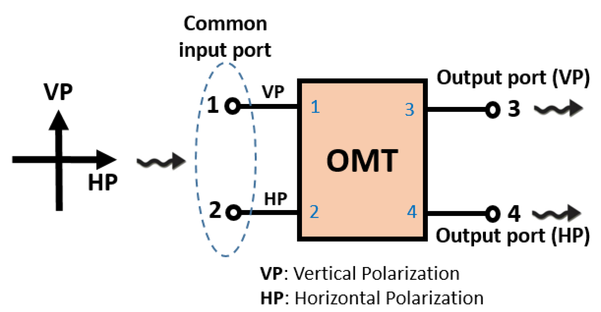
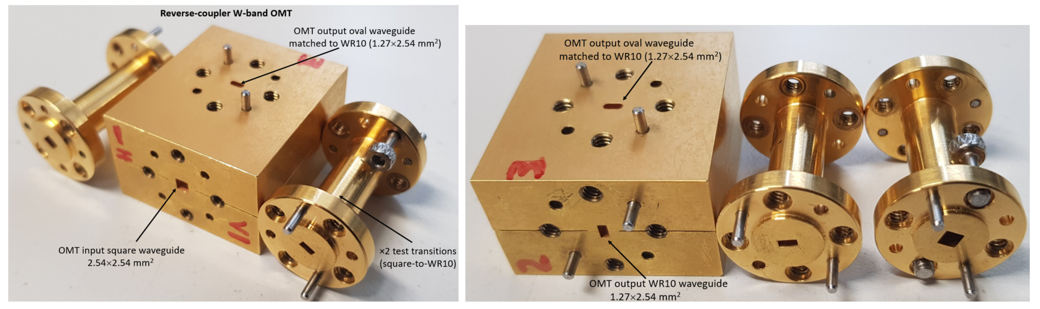
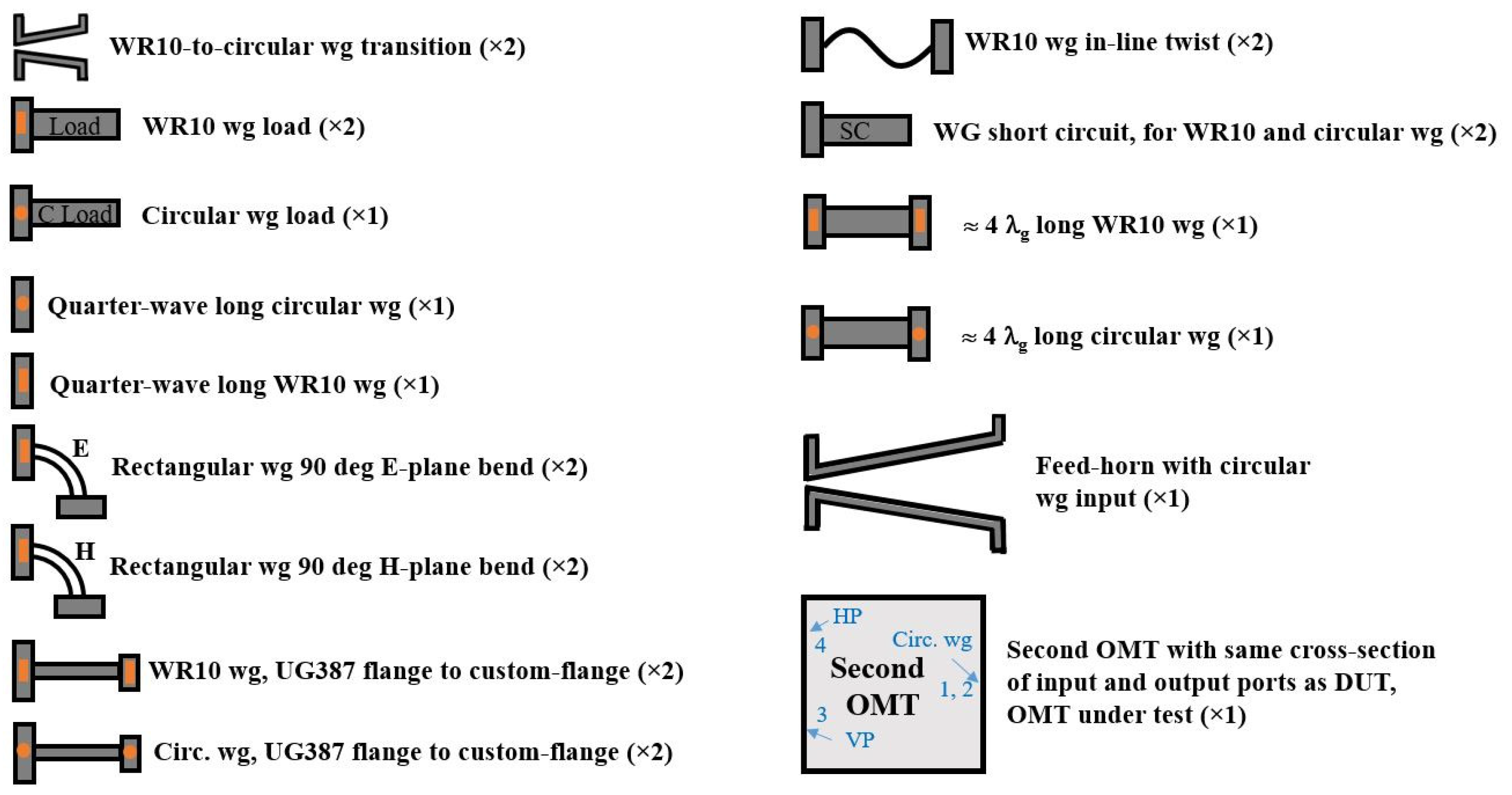
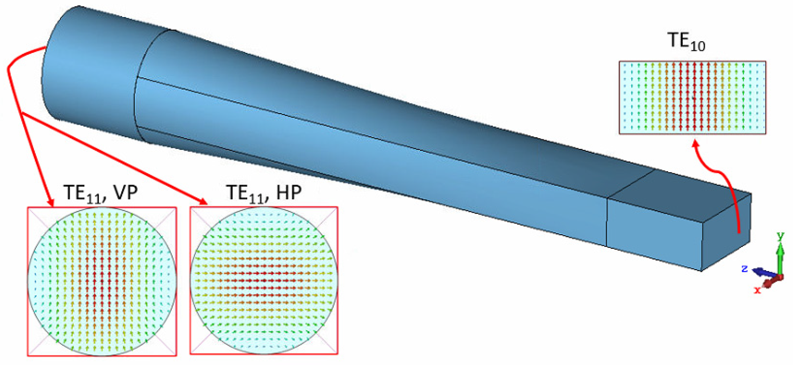
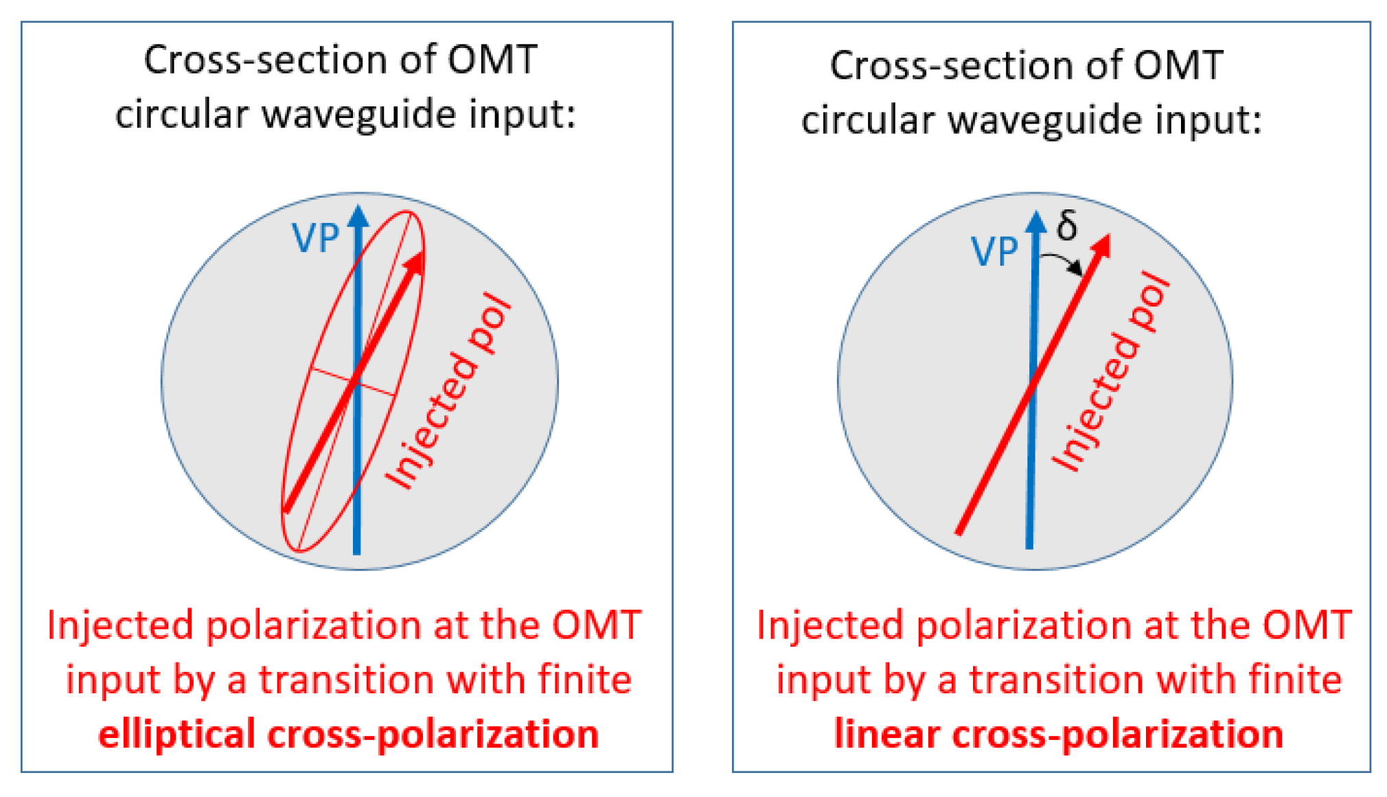
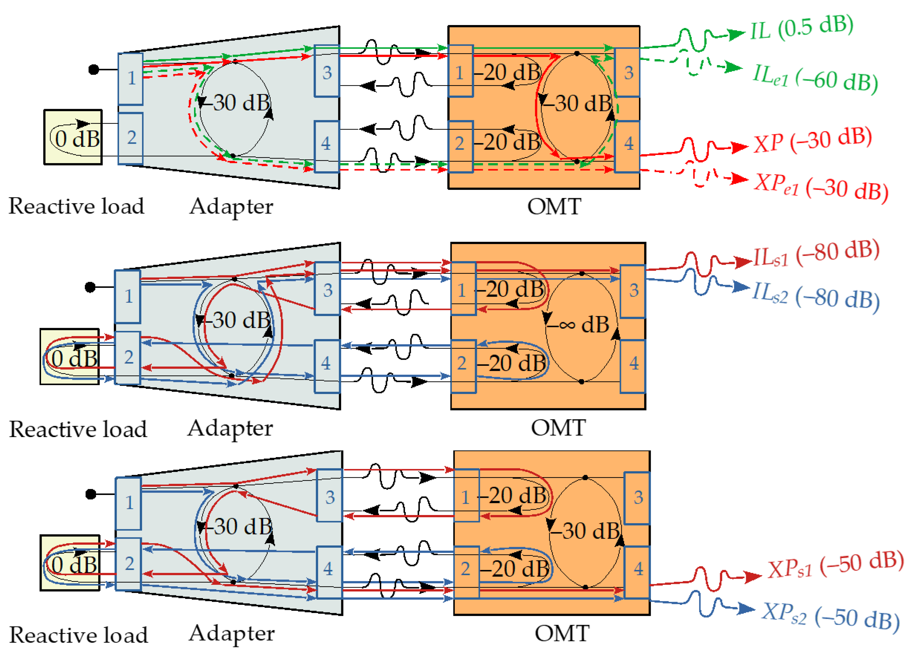
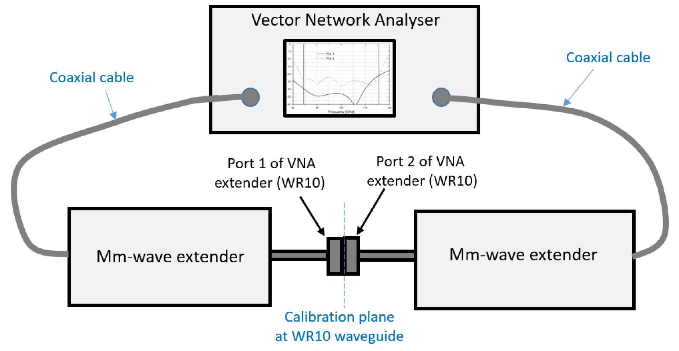
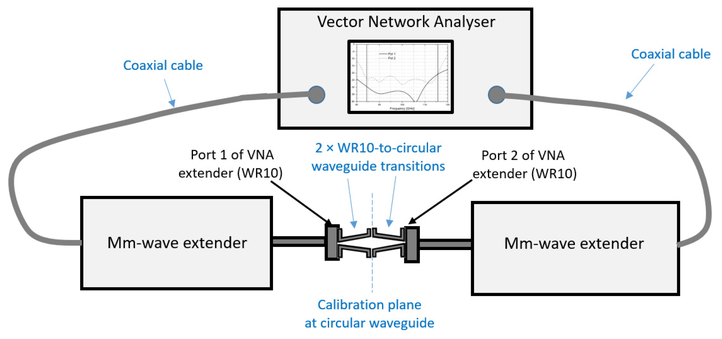
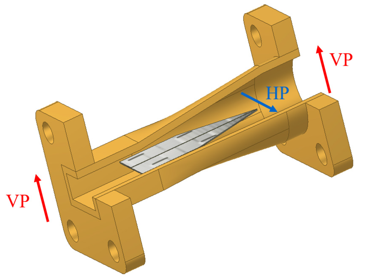
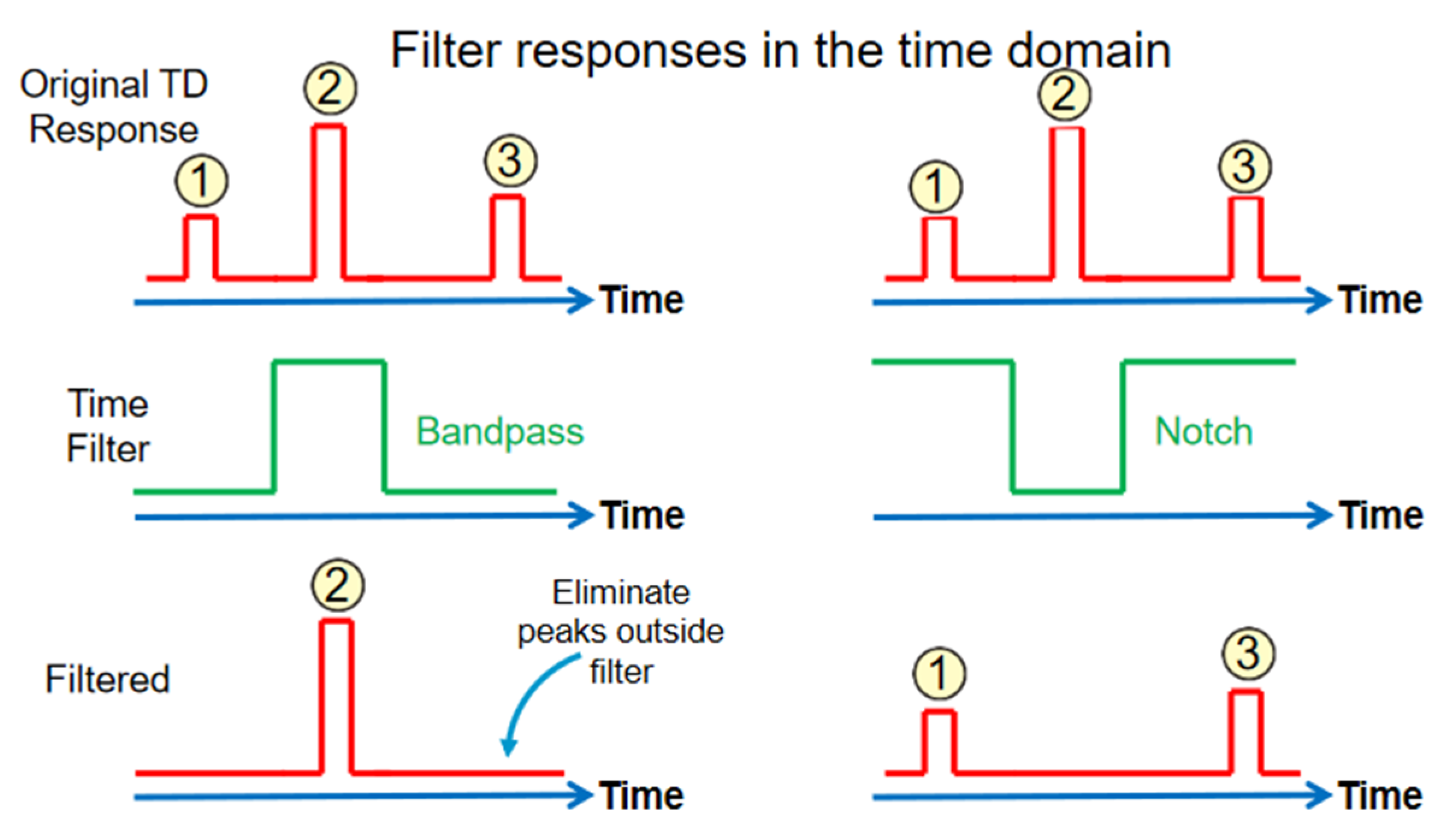
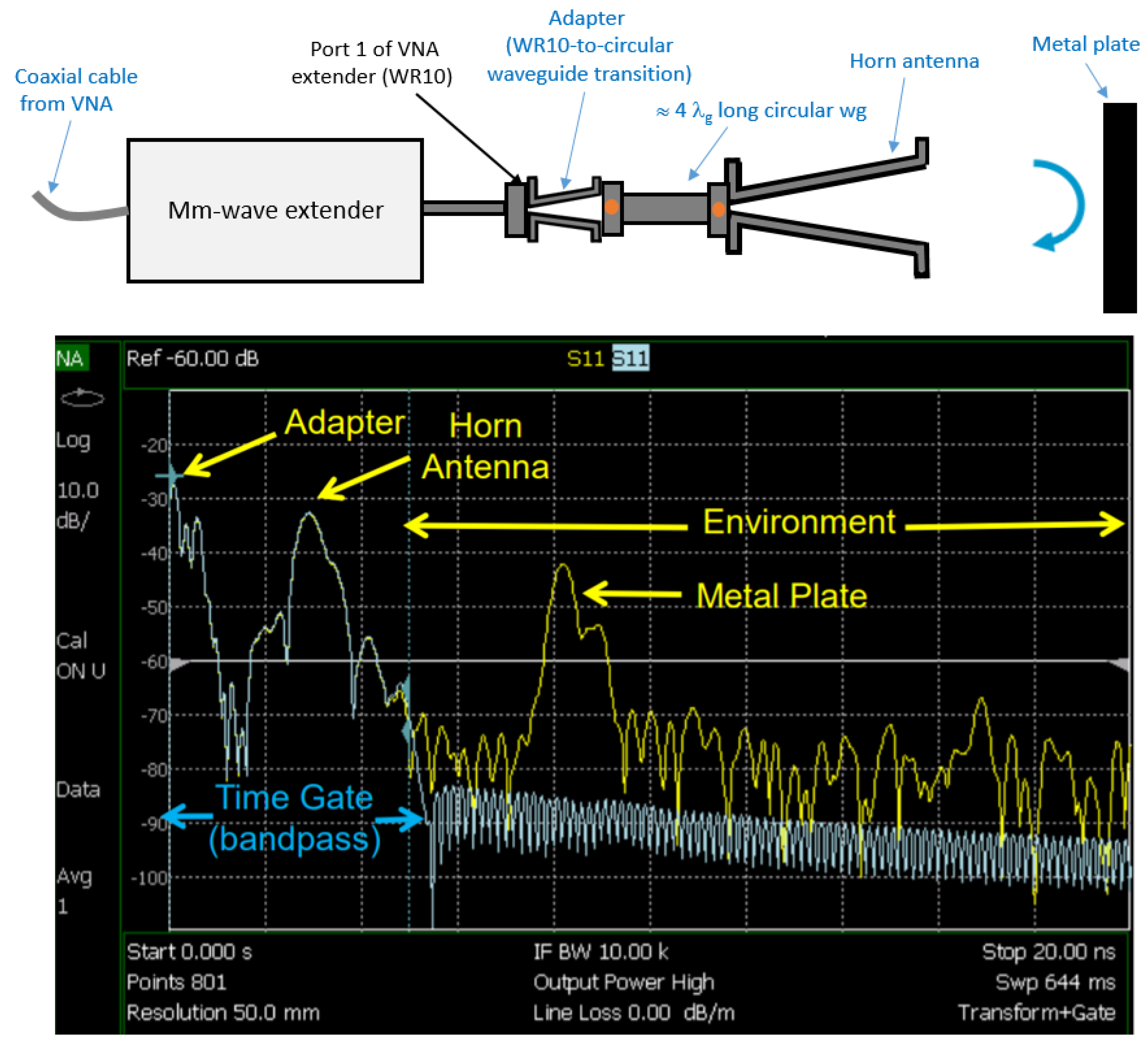
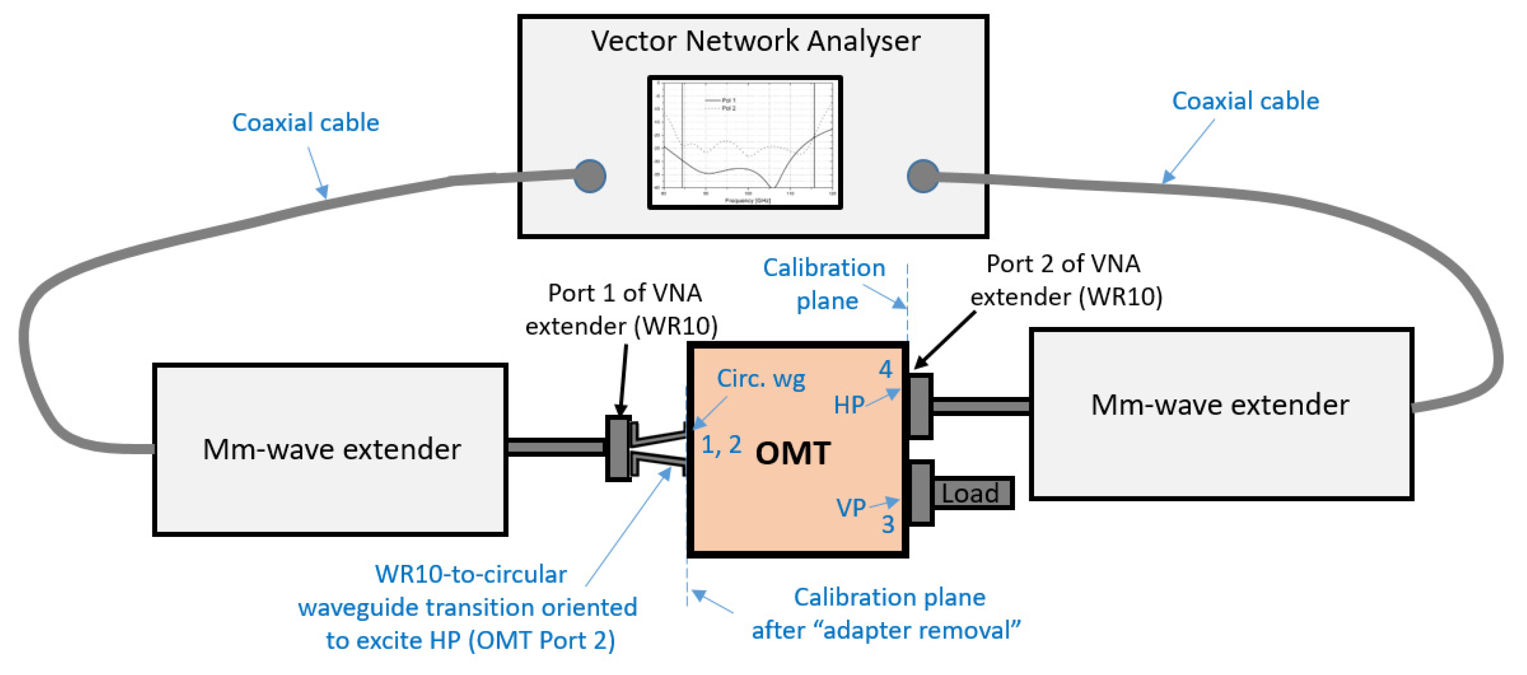
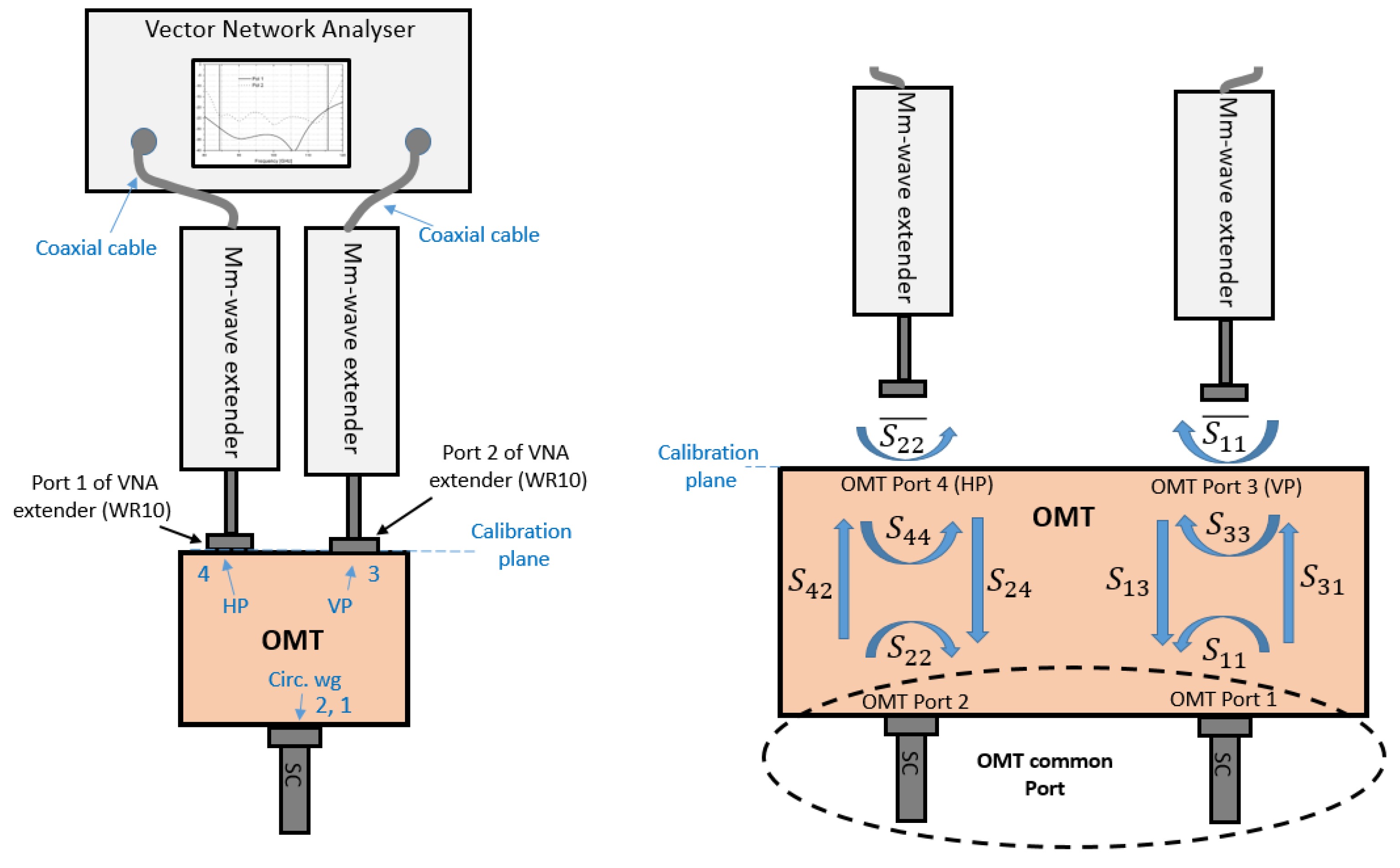
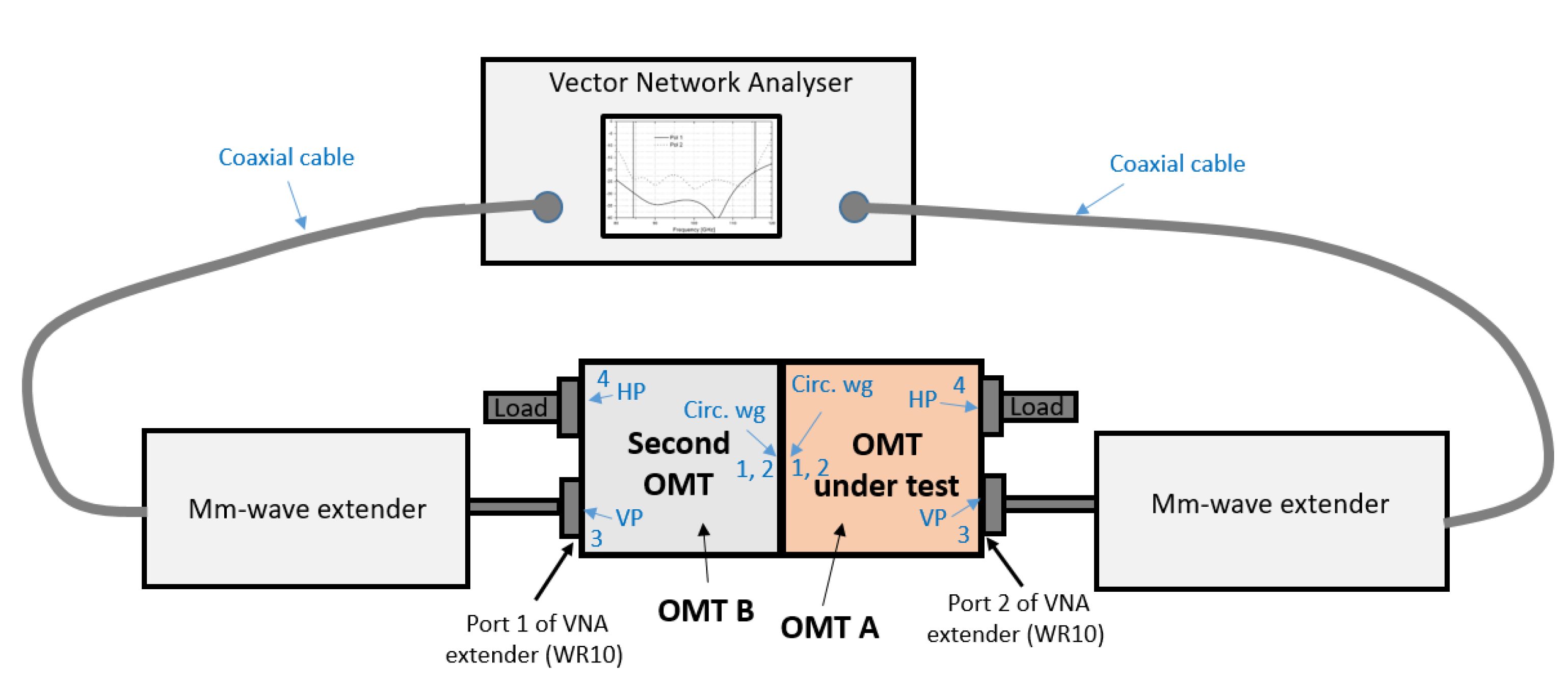
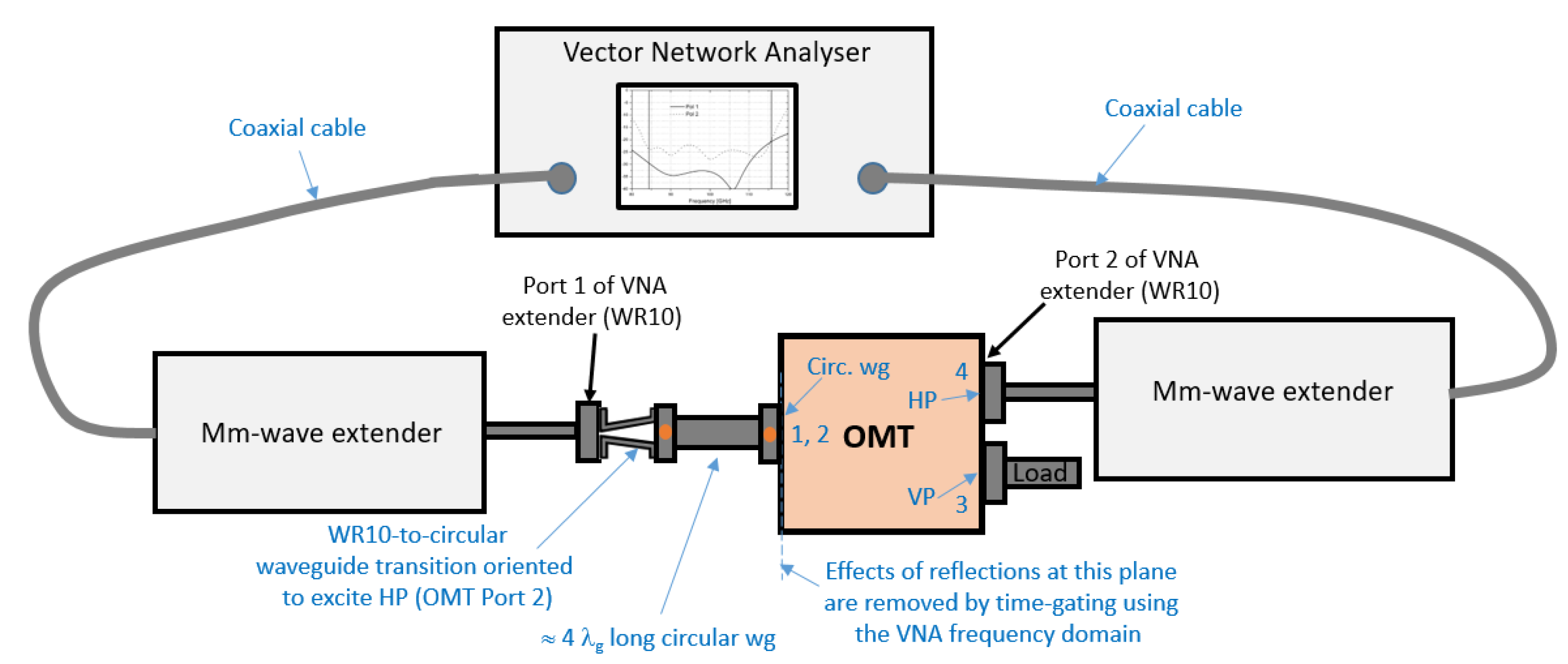
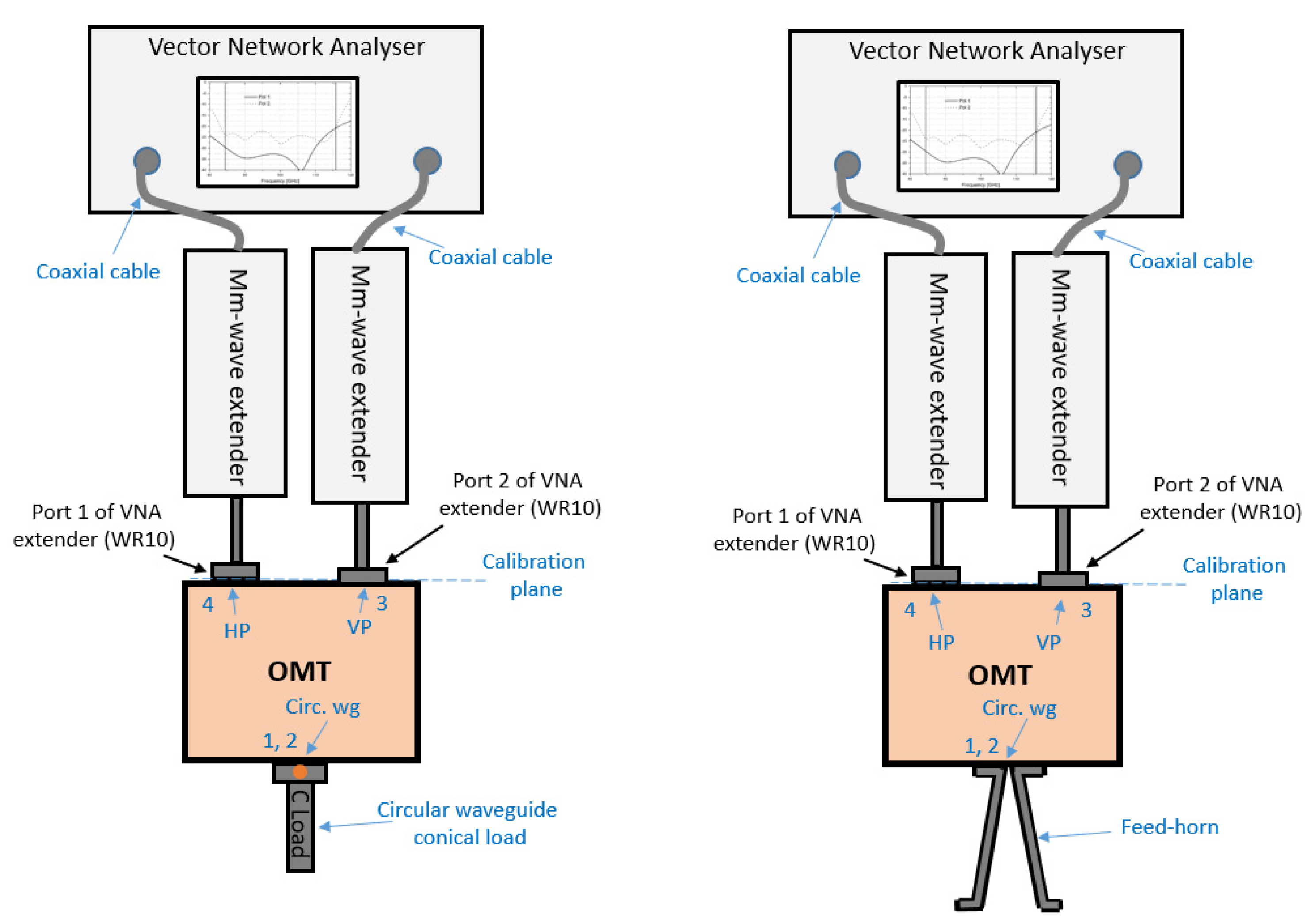
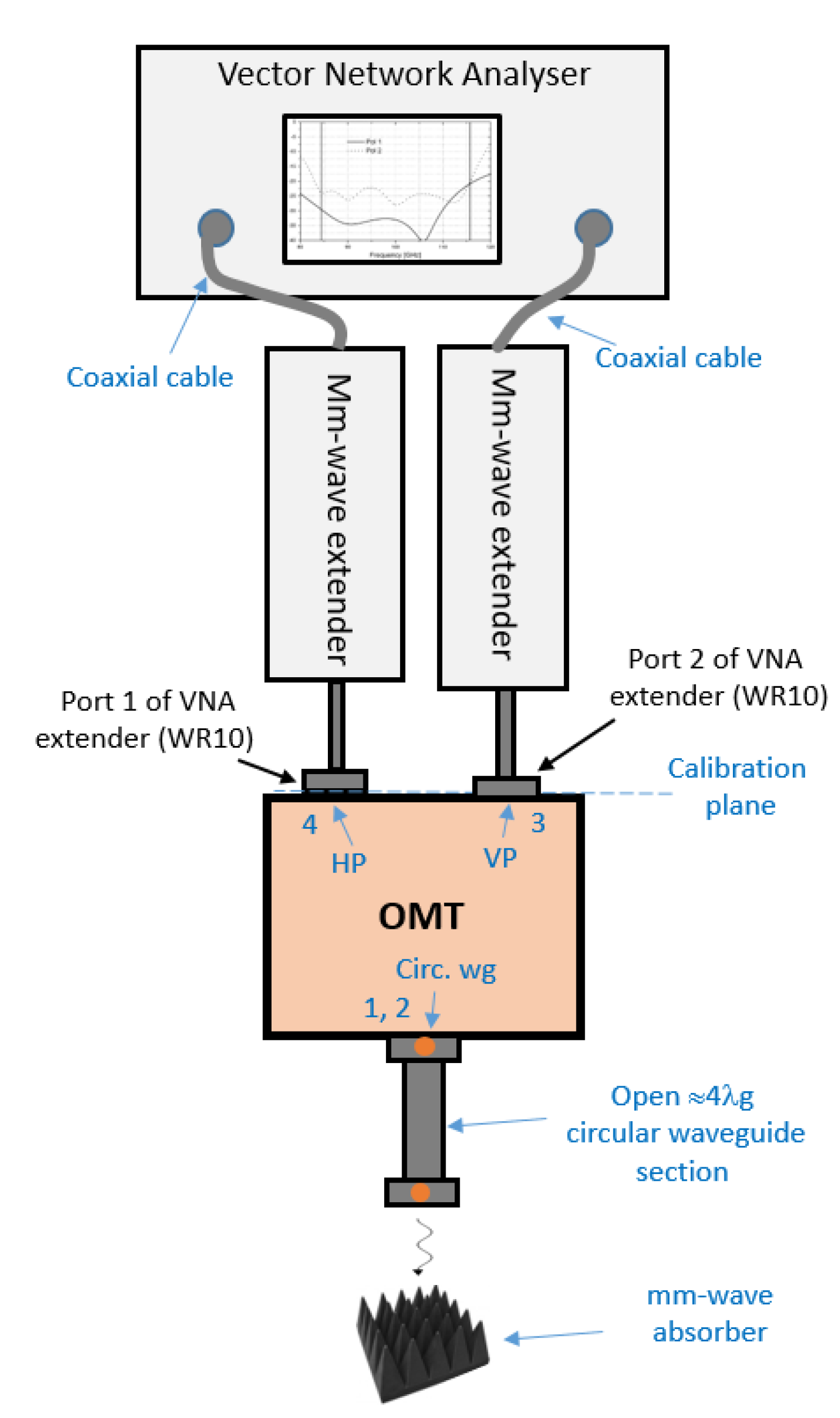
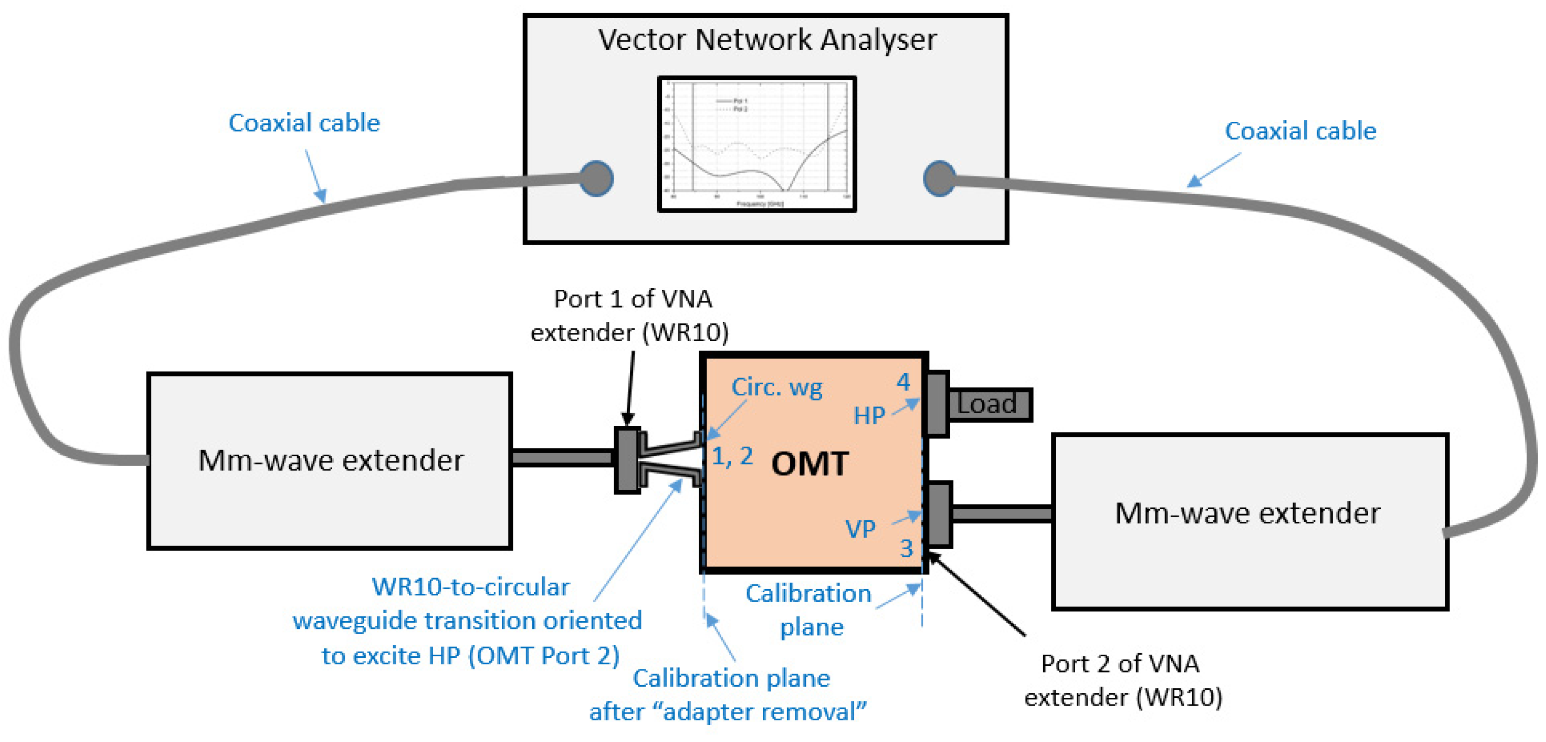
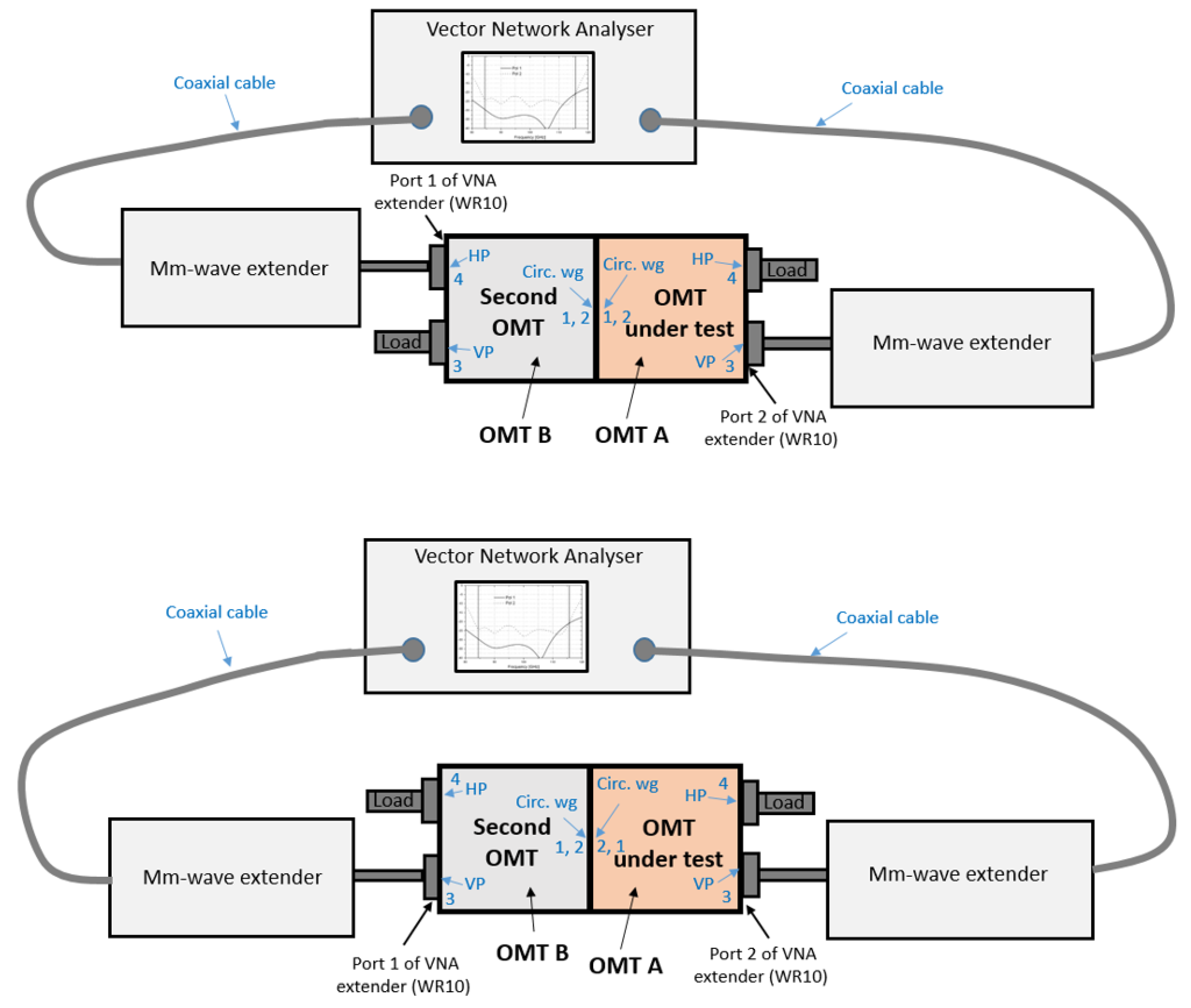
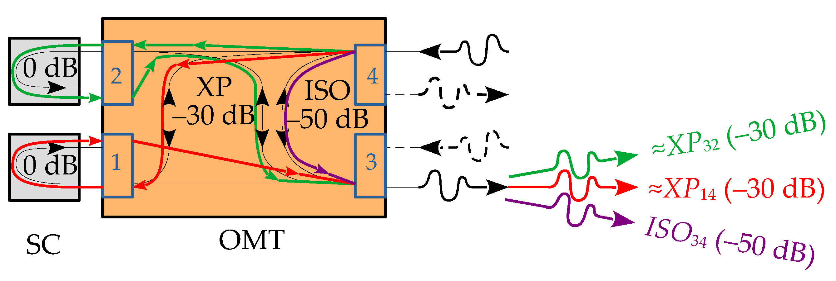
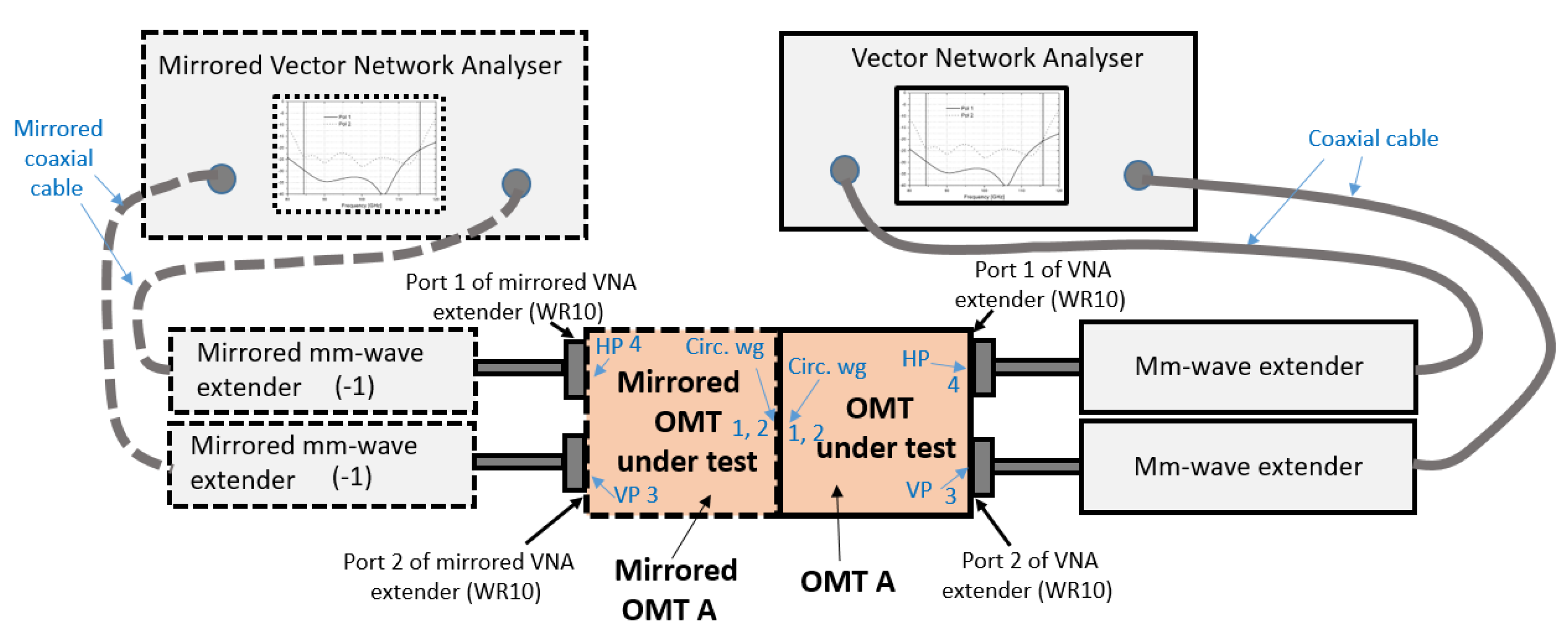
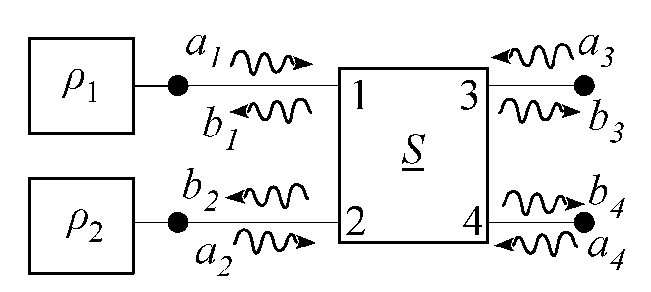
Table 1.
OMT specification to be met at the physical temperature of 293 K. The OMT operating temperature is ≈20 K.
Table 1.
OMT specification to be met at the physical temperature of 293 K. The OMT operating temperature is ≈20 K.
| Performance Parameter | Reference S-Parameter | Specification |
|---|---|---|
| Frequency range | - | 84–116 GHz |
| Insertion Loss of signal VP from Port 1 to output Port 3, IL31 | |S31| | <0.5 dB |
| Insertion Loss of signal HP from Port 2 to output Port 4, IL42 | |S42| | <0.5 dB |
| Input Return Loss of signal VP at Port 1, IRL11 | |S11| | >20 dB |
| Input Return Loss of signal HP at Port 2, IRL22 | |S22| | >20 dB |
| Output Return Loss of signal VP at Port 3, ORL33 | |S33| | >20 dB |
| Output Return Loss of signal HP at Port 4, ORL44 | |S44| | >20 dB |
| Cross-polarization of signal VP from Port 1 to output Port 4, XP41 | |S41| | >30 dB |
| Cross-polarization of signal HP from Port 2 to output Port3, XP32 | |S32| | >30 dB |
| Isolation between Port 3 and Port 4, ISO43 | |S43| | >30 dB |
| Isolation between Port 4 and Port 3, ISO34 | |S34| | >30 dB |
Publisher’s Note: MDPI stays neutral with regard to jurisdictional claims in published maps and institutional affiliations. |
© 2021 by the authors. Licensee MDPI, Basel, Switzerland. This article is an open access article distributed under the terms and conditions of the Creative Commons Attribution (CC BY) license (https://creativecommons.org/licenses/by/4.0/).
Share and Cite
MDPI and ACS Style
Navarrini, A.; Nesti, R. Characterization Techniques of Millimeter-Wave Orthomode Transducers (OMTs). Electronics 2021, 10, 1844. https://0-doi-org.brum.beds.ac.uk/10.3390/electronics10151844
AMA Style
Navarrini A, Nesti R. Characterization Techniques of Millimeter-Wave Orthomode Transducers (OMTs). Electronics. 2021; 10(15):1844. https://0-doi-org.brum.beds.ac.uk/10.3390/electronics10151844
Chicago/Turabian StyleNavarrini, Alessandro, and Renzo Nesti. 2021. "Characterization Techniques of Millimeter-Wave Orthomode Transducers (OMTs)" Electronics 10, no. 15: 1844. https://0-doi-org.brum.beds.ac.uk/10.3390/electronics10151844
Note that from the first issue of 2016, this journal uses article numbers instead of page numbers. See further details here.