A Study on the Variable Inductor Design by Switching the Main Paths and the Coupling Coils


1
Department of Electrical Engineering, National Chung Hsing University, Taichung City 402202, Taiwan
2
Department of Electronic Engineering, National Chin-Yi University of Technology, Taichung City 411030, Taiwan
3
Department of Electronic Engineering, National Formosa University, Yunlin County 632301, Taiwan
*
Author to whom correspondence should be addressed.
Electronics 2021, 10(15), 1856; https://0-doi-org.brum.beds.ac.uk/10.3390/electronics10151856
Submission received: 28 June 2021
/
Revised: 24 July 2021
/
Accepted: 29 July 2021
/
Published: 2 August 2021
(This article belongs to the Section Microelectronics)
Abstract
:In a radio frequency (RF) system, it is possible to use variable inductors for providing tunable or selective frequency range. Variable inductors can be implemented by the microelectromechanical system (MEMS) process or by using transistors as switches to change the routing of coils or coupling quantities. In this paper, we investigated the design method of a variable inductor by using MOS transistors to switch the main coil paths and the secondary coupled coils. We observed the effects of different metal layers, turn numbers, and layout arrangements for secondary-coupled coils and compared their characteristics on the inductances and quality factors. We implemented two chips in the 0.18 μm CMOS process technology for each kind of arrangement for verification. One inductor can achieve inductance values from about 300 pH to 550 pH, and the other is between 300 pH and 575 pH, corresponding to 59.3% and 62.5%, respectively, inductance variation range at 4 GHz frequency. Additionally, their fine step sizes of the switched inductances are from 0.5% to 6% for one design, and 1% to 12.5% for the other. We found that both designs achieved a large inductance tuning range and moderate inductance step sizes with a slight difference behavior on the inductance variation versus frequency.
1. Introduction
In radiofrequency (RF) applications, inductors and capacitors are usually used to form the load impedances, matching networks, etc. It is the trend that the RF front end concurrently supports different standards. For such a system, reconfigurable circuits and architectures will be required. For providing tunable or selective frequency ranges, switched capacitors or varactors are easier to design and implement, compared with variable inductors. However, ongoing efforts seek to design a suitable variable inductor. The most common method to design a variable inductor is the microelectromechanical system (MEMS) process [1,2,3,4]. Although these MEMS variable inductors may have good quality (Q) factors and higher self-resonance frequencies (SRF), with the ability of continuous tuning, they are difficult to integrate with other circuits that utilize the conventional CMOS process technologies.
Besides MEMS approaches, variable inductors can also be implemented by using transistors as switches to change routing paths of coils or coupling quantities. The simplest way is using CMOS transistors as switches to short or open an inductor that is in series with another inductor [5]. This method occupies a larger area for using two inductors, and the inductances can be changed by only two discrete values. Stacked multilayers [6] or proper routing [7] may resolve the area issue, but they can still not provide flexible inductance tuning. Another possible mechanism for changing the inductance is to vary the mutual coupling between coils [8]. By switching the transistors on the secondary coupling loops, the mutual inductance between the main coil and the coupling coils will be changed; therefore, the resultant inductance of the main coil can be controlled. However, the inductance can still be switched as limited discrete values of large step sizes. The switching mutual inductance method is then extended to add some small coupling coils inside and outside of the main coils [9]. It can be shown that coarse steps of the inductance can be obtained by switching routing of main coils, and fine steps of the inductance can be obtained by switching the additional small coupling coils. Although this design seems to provide both coarse and fine-tuning of the inductance, we noticed that the fine-tuning step is too small to provide significant tuning in frequency, and large inductance gaps exist between coarse steps.
In this paper, we adopted a similar method as in [9] but used bottom metal layers to form the secondary coupling coils; thus, we can maximize the mutual coupling between the main coils and controlled coupling coils. We also tried multi-turns for the secondary coupling coils to investigate their influence on the inductance. The rest of this paper is structured as follows: Detailed design considerations are given in Section 2, and the experimental results are shown in Section 3. Finally, a simple conclusion is made in Section 4.
2. Variable Inductor Design
As mentioned in the previous section, a variable inductor can be realized by using CMOS transistors as switches to change the path of the main coils and/or the secondary coupling coils. Kossel et al. [9] proposed a variable inductor design adopting such a technique, both in main coils and secondary coupling coils. The authors sought to maximize the Q-factor of the secondary coupling coils; thus, they chose the thick top metal layer to implement both their main coils and secondary coupling coils. However, this choice limited the secondary coupling coils’ area size, and all secondary coupling coils are of the one-turn path. Additionally, the resultant mutual coupling between the main coil and the secondary coupling coils is too small to provide significant inductance change. To maximize the overlapping area of the main coil and the secondary coupling coils, our efforts were to design the secondary coupling coils using the lower metal layers. The relation between the one-turn main coil and the one-turn secondary coupling coil has been comprehensively studied in the previous work [10]. Although the target of design in [8,10] is mainly to enlarge the inductance change, the analyses and equations provided in [10] still fit our secondary coupling coils design. However, the effects of different metal layers, turn numbers, and area sizes were not studied, and our target is to provide a moderate inductance step size. We first investigated the influence of different metal layers on mutual coupling. Then, we observed the difference of mutual coupling for the secondary coils being one turn or two turns. After these two investigations on the secondary coupling coils, we studied the influence of the area size of the secondary coupling coils. Then, we described the influence of the size of CMOS transistors and the design of main coils. All the simulations in this section were based on the 0.18 μm 1P6M CMOS process technology.
2.1. Influence of Metal Layer for Secondary Coupling Coil of One Turn
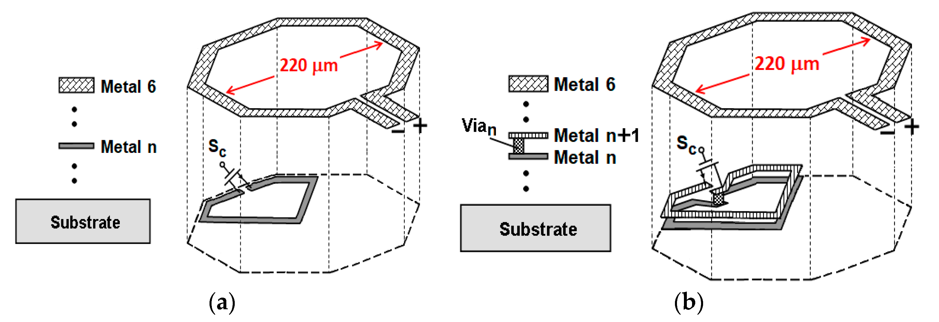
To investigate the mutual coupling for different metal layers of secondary coupling coil, we used a one-turn octagon shape at top metal (Metal 6) as the main coil and lower metal layer (Metal n; n = 1–5) to form the secondary coupling coil, as shown in Figure 1a. For our design purposes, the shape of the secondary coupling coil occupies approximately one-fourth of the main coil projection area. The width of the main coil is 15 μm, and the width of the secondary coupling coil is 9 μm. For each metal layer of the secondary coupling coil, we generated a similar layout and performed an electromagnetic (EM) simulation to obtain the mutual coupling between the two kinds of coils. The switch Sc in Figure 1a is set to be ideally short-circuited or ideally open-circuited to compare the difference of the inductance and the Q factor of the main coil. When Sc is open-circuited, the simulated main coil inductances are almost the same regardless of the metal layer used in the secondary coupling coil. The simulated inductances under open-circuited Sc are about 534.6 pH, 547.1 pH, and 570 pH for 4 GHz, 8 GHz, and 12 GHz, respectively. The simulated Q factors under open-circuited Sc are about 10.88, 15.5, and 15.0 for 4 GHz, 8 GHz, and 12 GHz, respectively. Table 1 shows the simulated inductance changes in percentage and Q factors for different metal layers of secondary coupling coil under short-circuited switch Sc. Since the induced current in the secondary coupling coil is in the opposite direction according to Lenz’s law, the mutual coupling between the main coil and the secondary coupling coil is negative, which causes a decrease in the inductance of the main coil. It can be seen that the mutual coupling increases as the secondary coupling coil is closer to the main coil for a higher metal layer. In the meantime, the Q factor also decreases as the secondary coupling coil is closer to the main coil. The relation between the inductance change and the Q factor is a trade-off.
2.2. Influence of Metal Layer for Secondary Coupling Coil of Two Turns
To compare the mutual coupling for two-turn secondary coupling coils, we also used a one-turn octagon shape at top metal (Metal 6) as the main coil and lower metal layers (Metal n and n + 1; n = 1–4) to form the secondary coupling coil, as shown in Figure 1b. The geometry parameters are the same as those in Figure 1a, except for the secondary coupling coil occupying two bottom metal layers to form a two-turn coil. The switch Sc in Figure 1b is still set to be ideally short-circuited or ideally open-circuited, as in the previous subsection. When Sc is open-circuited, the simulated main coil inductances are almost the same regardless of the metal layer used in the secondary coupling coil. The simulated inductances under open-circuited Sc are about 527.9 pH, 540 pH, and 566 pH for 4 GHz, 8 GHz, and 12 GHz, respectively. The simulated Q factors under open-circuited Sc are about 10.9, 15.6, and 15.2 for 4 GHz, 8 GHz, and 12 GHz, respectively. Table 2 shows the simulated inductance changes in percentage and Q factors for different metal layers of secondary coupling coil under short-circuited switch Sc. There is still a trade-off between the inductance change and the Q factor. It can be found that the inductance change of the two-turn secondary coupling coil of metal n and n+1 is approximately 1.21 to 1.35 times that of the one-turn case of metal n. The Q factor is better than the counterpart of the one-turn case.
2.3. Influence of Area Size for Secondary Coupling Coil
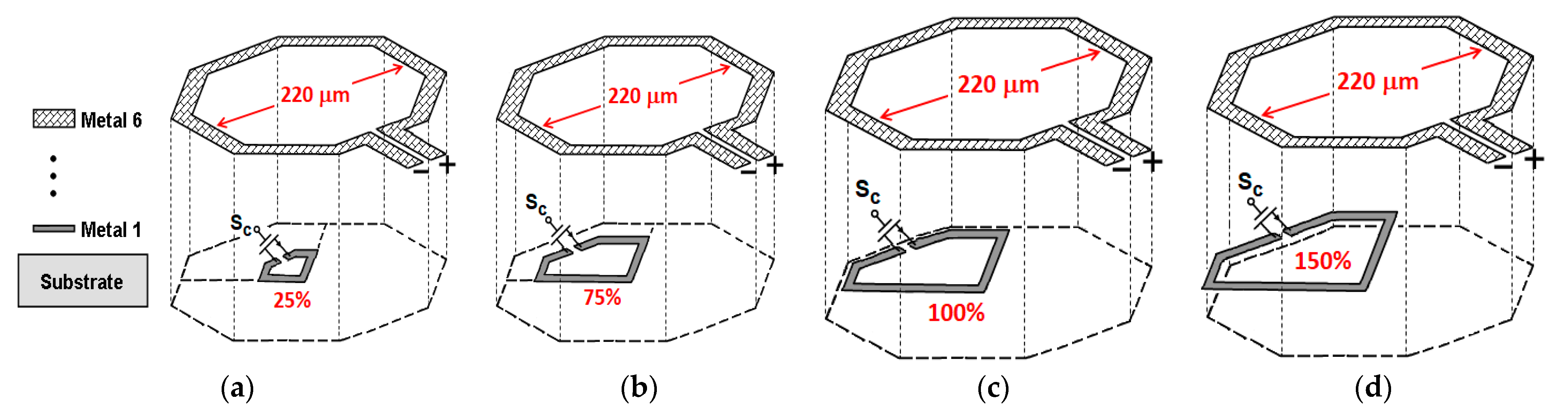
To investigate the mutual coupling for different area sizes of the secondary coupling coil, we used a one-turn octagon shape at top metal (Metal 6) as the main coil and the most bottom metal layer (Metal 1) to form the secondary coupling coil, as shown in Figure 2a–d, which is similar to those in Section 2.1, but the secondary coupling coils occupies different area percentage from that in Figure 1a. The width of the main coil is still 15 μm, whereas the width of the secondary coupling coil is also 9 μm. Referring to Figure 2a–d, we simulated the percentages of 25%, 50% (not shown in Figure 2), 75%, 100%, and 150%. The simulated inductances under open-circuited Sc are the same as in Figure 1a and are about 534.6 pH, 547.1 pH, and 570 pH for 4 GHz, 8 GHz, and 12 GHz, respectively. The simulated Q factors under open-circuited Sc are about 10.88, 15.5, and 15.0 for 4 GHz, 8 GHz, and 12 GHz, respectively. Table 3 shows the simulated inductance changes in percentage and Q factors for different area percentages of secondary coupling coil under short-circuited switch Sc. It can be seen that the mutual coupling increases as the area of the secondary coupling coil increases, without exceeding the projection of the main coil area.
In the meantime, the Q factor also decreases, as the overlapping area of the secondary coupling coil with the main coil is larger. From the case of 150%, the change in inductance will decrease because the secondary coupling coil encloses both the areas inside and outside of the projection of the main coil and the magnetic fields are opposite in direction for these two areas. The dependence of overlapping area on the change in inductance is a positive correlation but not with the proportion. Again, the relation between the inductance change and the Q factor is a trade-off.
2.4. Influence of Transister Size for Secondary Coupling Coil
In the previous simulations, we used an ideal short- or open-circuited design to investigate the effects of different metal layers, turn numbers, and area percentages of layout arrangement. In this subsection, we used the NMOS model in the simulation, in which the test geometry was as the arrangement shown in Figure 1b, and the two-turn secondary coupling coil was formed by metal 1 and 2, i.e., the most bottom two metal layers. The transistors were chosen to be NMOS with a channel length of 180 nm. From the summary shown in Table 4, it was found that both the inductance changes and Q factors increase as the NMOS sizes (W/L) increase. However, the SRF of the inductor also drops down significantly as the NMOS switches sizes increase. In the case of W = 300 μm case, the SRF drops to around 12 GHz, and this influences the inductance change percentage at that frequency. Therefore, we need to trade off the requirements of inductance tuning ability, Q factor, and SRF.
2.5. Main Coil Design
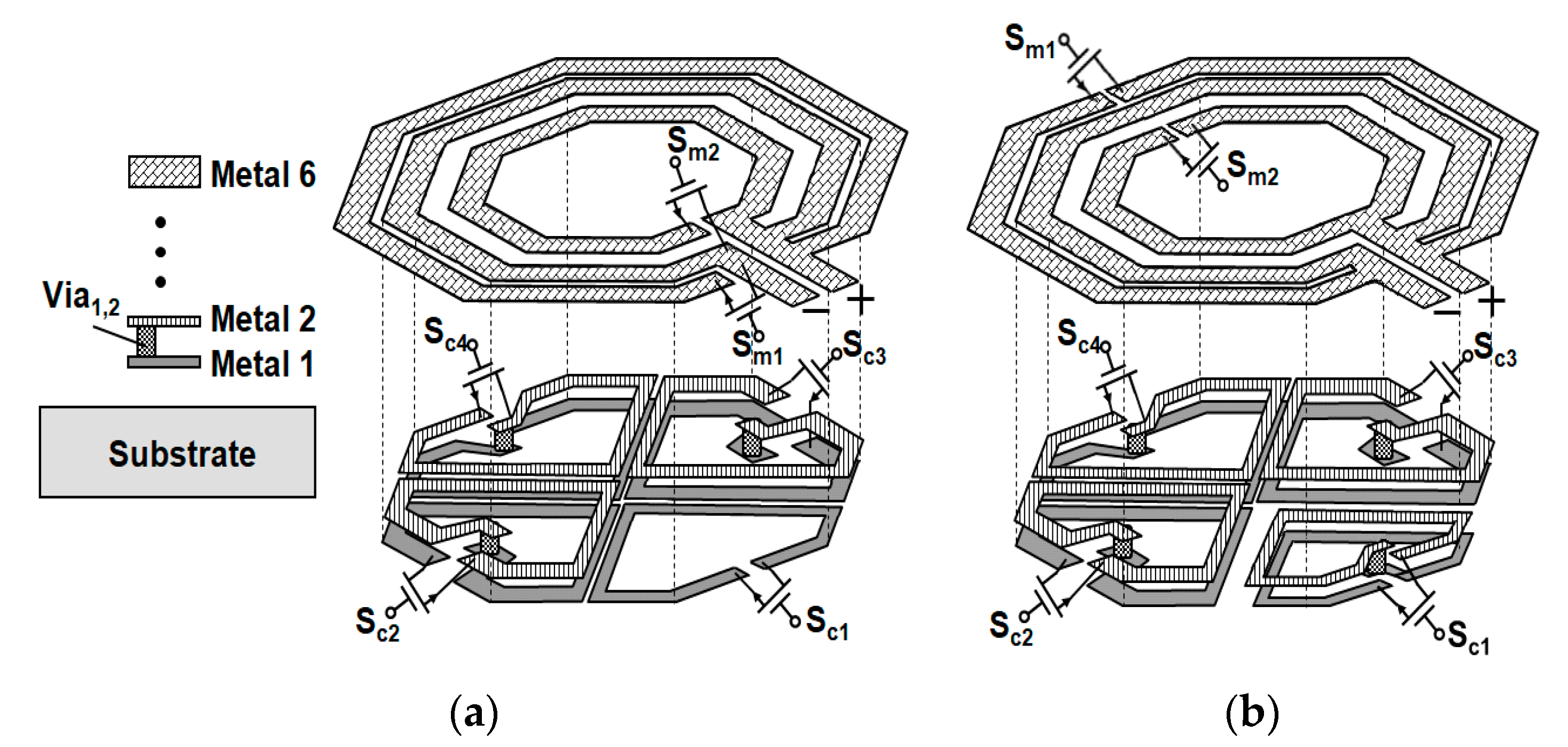
For all the simulated cases we discussed above, the secondary coupling coils occupy only one-quarter of the projection area of the main coil. The largest percentage of inductance change is about 13%, which implies that the largest percentage of inductance change will not exceed 40% even if we fulfill the entire projection area with four similar secondary coupling coils. To extend the range of variable inductance, we also switched the paths of the main coil, as carried out in [9]. For the secondary coupling coils, although the single turn design using metal 5 or two-turn design using metals 4 and 5 have a larger percentage of inductance change, its SRF may be relatively low due to the small distance between metal layers 5 and 6. Therefore, we adopted a two-turn design by using metal 1 and 2 layers, which can provide acceptable fine-tuning inductance change with a better Q factor. The illustrations of the final two designs are shown in Figure 3a,b. In Figure 3a, we used three similar two-turn secondary coupling coils with a one-turn coil, and by changing the combination of the state of the switches Sc1 to Sc4, we can obtain seven kinds of fine-tuned conditions. In addition, coarse tuning is achieved by switching the switches Sm1 and Sm2, which can change the current paths in the main coils. The function of Sm2 is relatively easy to understand in that it provides a shorter path and thus makes the inductance smaller if Sm2 is short-circuited. The function of a turning-on switch Sm1 is such that it can push the current distribution toward the center due to the proximity effect, and this also makes the inductance smaller. The design of Figure 3b is similar to that in Figure 3a except for the replacement of a two-turn secondary coupling coil with a smaller area rather than a one-turn coil and for the positions of switches Sm1 and Sm2. By switching both switches in main coils and secondary coupling coils, we can obtain coarse and fine-tuning of the inductance in the main coil. The mutual coupling by turning on Sc2–Sc4 is almost the same, whereas the mutual coupling by turn-on Sc1 is smaller than others. The effective turn number controlled by Sc1 can be seen as one turn and Sc2–Sc4 can be seen as two turns. By different combinations of the status of switches Sc1–Sc4, the effective turns (Neff) of the secondary coupling coils can vary from 0 (all switches turned off) to 7 (all switches turned on). To maintain the operation of the main coil as a symmetrical inductor, switches Sc2 and Sc3 should be turned on or off simultaneously. With the proper controlling design of main coils and secondary coupling coils, the inductance can vary over a large range with moderate step size without a large gap of inductance value in the whole inductance range.
The width of the main coils was chosen to be 15 μm. The inner radius of the inner, center, and outer paths of the main coils were 85 μm, 110 μm, and 127 μm, respectively. The width of the bottom secondary coupling coils was chosen to be 9 μm. We adopted NMOS transistors to implement the switches Sm1, Sm2, and Sc1 to Sc4. The influence of the transistor size for Sm1 and Sm2 is similar to the discussion made in Section 2.4. The NMOS transistors of Sm1 and Sm2 were chosen to be 4 μm/180 nm × 50 fingers for the main coils, while the NMOS transistors of Sc1–Sc4 were 5 μm/180 nm × 60 fingers for the bottom secondary coupling coils.
3. Experimental Results and Discussions
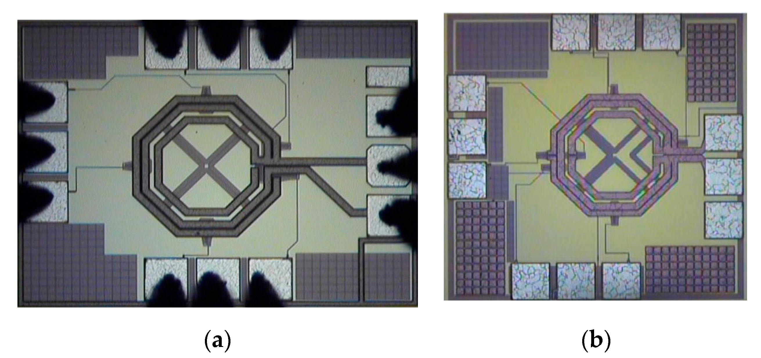
The proposed variable inductors were implemented in the 0.18 μm CMOS process technology. The micrographs of the proposed variable inductors are as shown in Figure 4a,b in which the chip sizes are 0.768 mm × 0.574 mm for the inductor in Figure 3a and Figure 4a, and 0.686 mm × 0.620 mm for the inductor in Figure 3b and Figure 4b. The s-parameter measurements for the proposed inductors were performed on the Agilent 8753ES network analyzer.
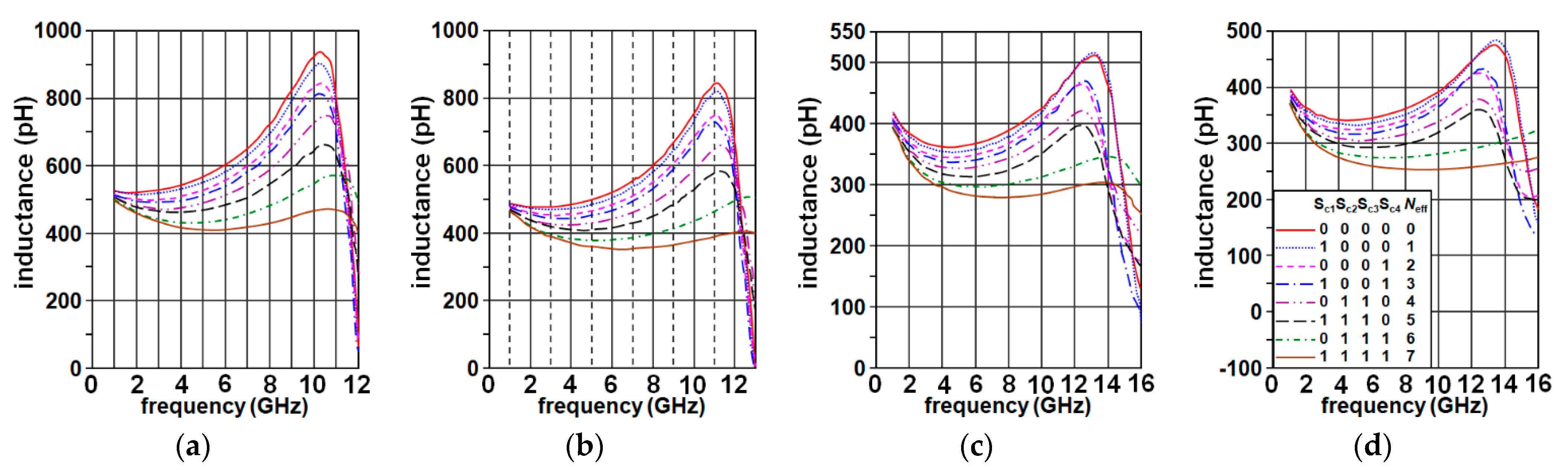
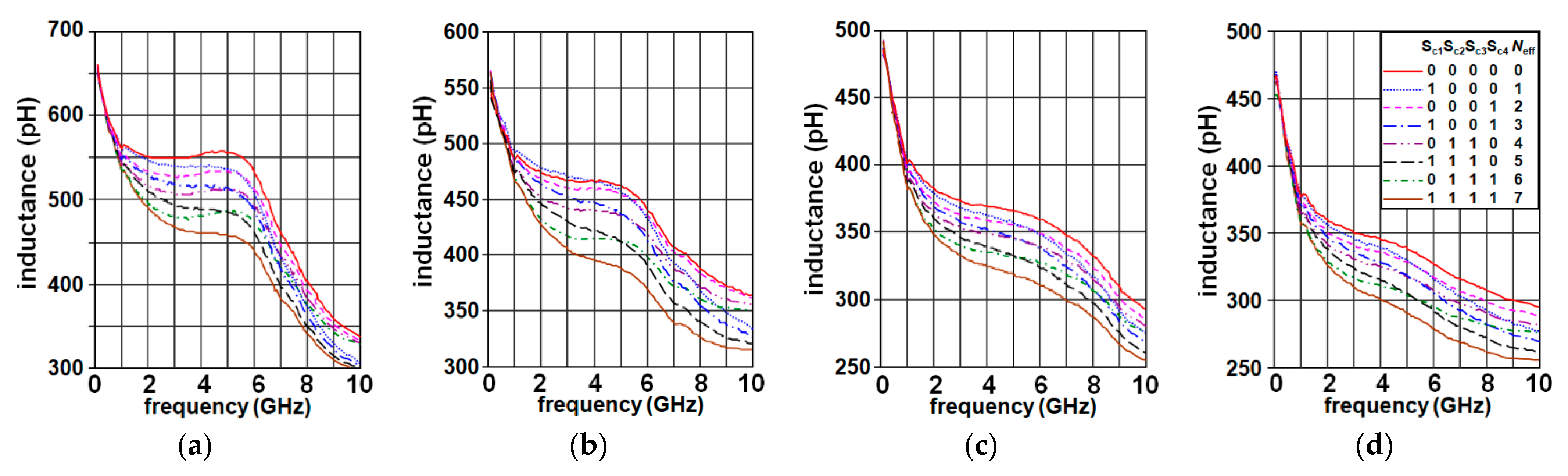
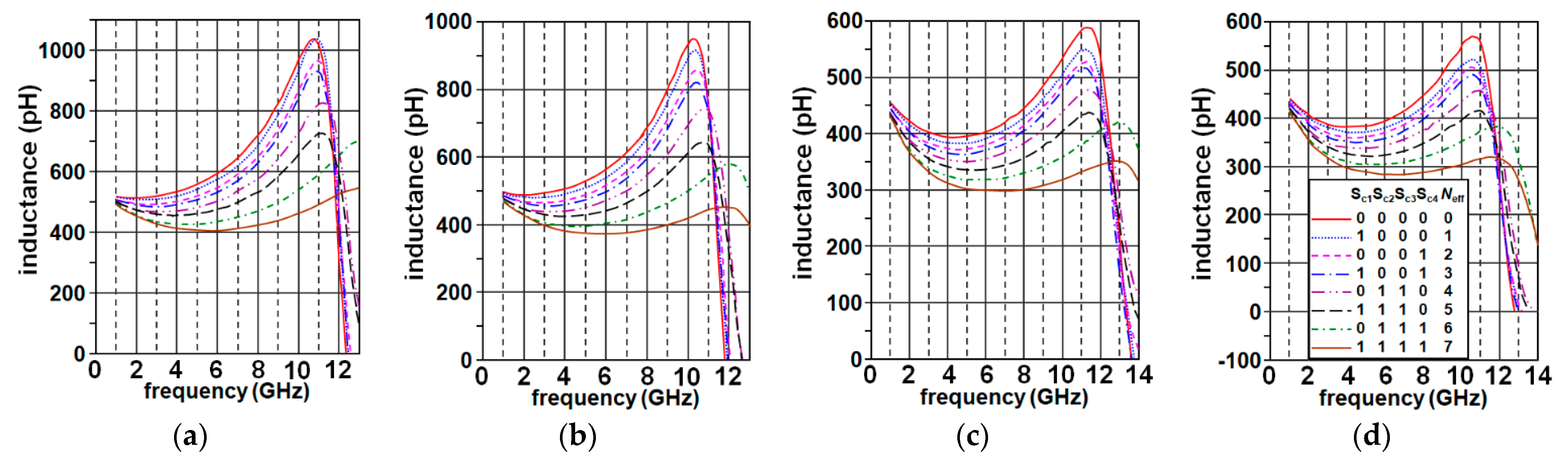
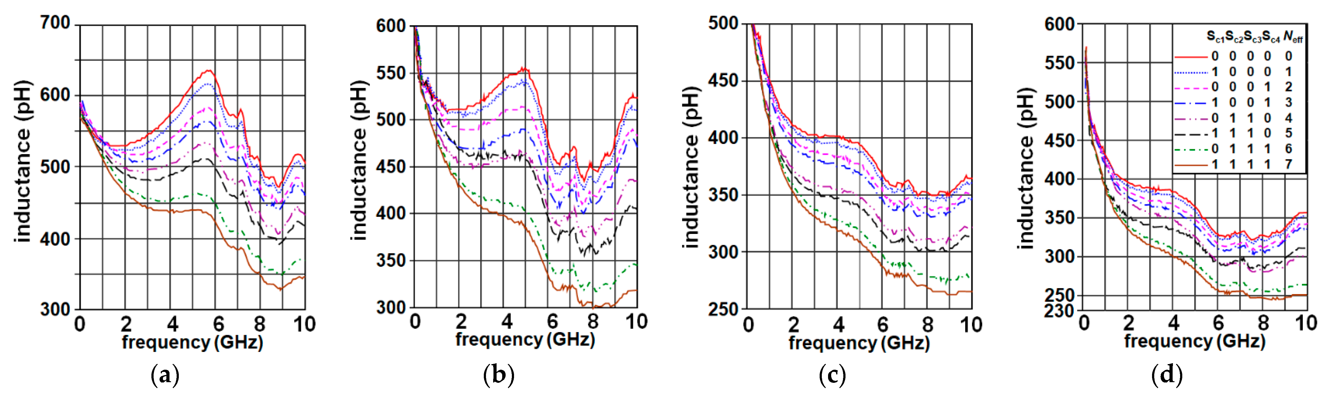
The simulated or measured resultant inductances were obtained by using the definition of the inductance: L = Im(Zin)/ω from s-parameters. Figure 5a–d shows the simulated inductances versus the frequencies of the proposed variable inductor in Figure 3a under different switch conditions for Sm1 and Sm2 in which “0” represents the OFF status, and “1” stands for the ON status. The eight curves in each subfigure represent the resultant inductances versus the frequencies for one of the eight possible combinations of Sc1 to Sc4 and the effective turns Neff mentioned in the previous subsection, as shown in the inset of Figure 5d. The corresponding measured results are as shown in Figure 6a–d. It can be seen that the inductances have coarse change steps by switching the status of Sm1 and Sm2. Additionally, it can also be investigated that fine step size can be achieved by switching the status of the secondary coupling coils. For the simulated results, the inductor has a peak inductance of 940 pH at 10.25 GHz for all switches being OFF and the lowest inductance of 255 pH at 9 GHz for all switches being ON. As for the measured case at the 4-GHz frequency, the largest inductance is 553 pH and the smallest inductance is 300 pH, corresponding to a change rate of the inductance of about 59.3%. Additionally, the fine step sizes of the switched inductances in Figure 6a–d are about 0.5% to 6.1% for most inductance range at 4 GHz. However, the frequency characteristic of the one-turn secondary coupling coil controlled by Sc1 has a slightly different trend, compared with the two-turn coils. Moreover, the inductances roll off for frequencies larger than 6 GHz due to additional parasitic capacitance and loss from switches.
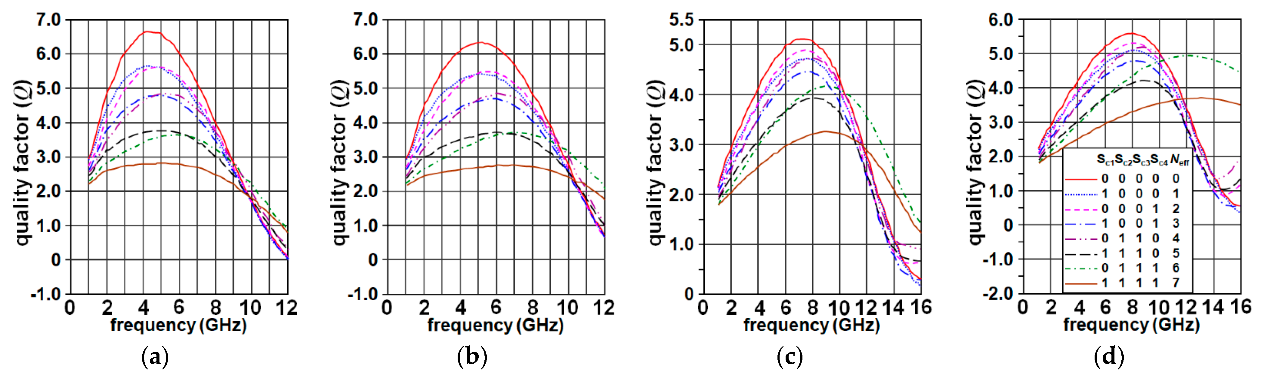
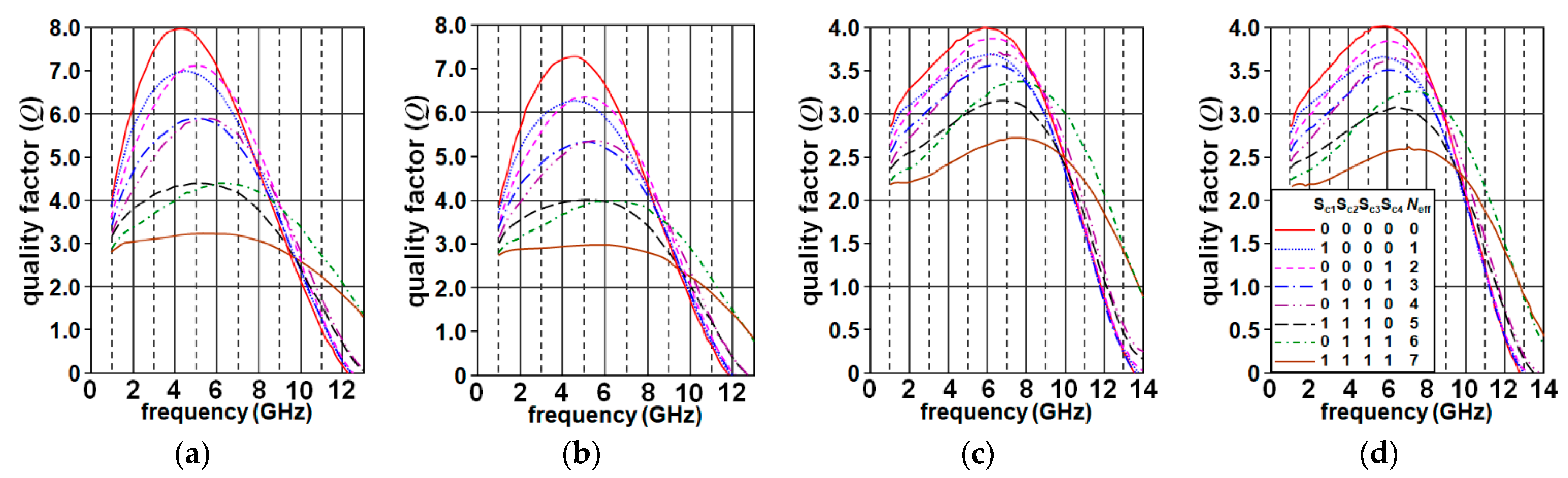
Figure 7a–d and Figure 8a–d show the corresponding simulated and measured Q factors versus the frequencies of the proposed inductor in Figure 3a and the eight curves in each subfigure are under the same control status as those in Figure 5a–d and Figure 6a–d except for the quantities are changed as the Q factors. The simulated and measured Q factors are obtained from the simulated or measured s-parameters by using the definition Q = Im(Zin)/Re(Zin). For the simulated results, it can be seen that the peaks of the Q factors occur at the frequency range from 4.1 GHz to 8.0 GHz depending on the status of the switches Sm1 and Sm2. There is a highest peak Q factor of 6.6 at 4.1 GHz for all switches being OFF, and there is a lowest peak Q factor of 2.8 at 5 GHz for Sm1 and Sm2 being OFF and Sc1–Sc4 being ON. As for the measured cases, it can be seen that the peaks of the Q factors occur at the frequency range from 2.0 GHz to 3.0 GHz for most of the cases which are obviously lower than the simulated ones. Additionally, the peak values of Q factors are from 2.8 to 4.7 depending on the status of switches. The values of Q factors are varied from 2.5 to 3.75 at the frequency of 4 GHz. Again, the frequency ranges of the measured Q factors are smaller than those obtained by simulation, and the values indicate that additional loss exists in real cases.
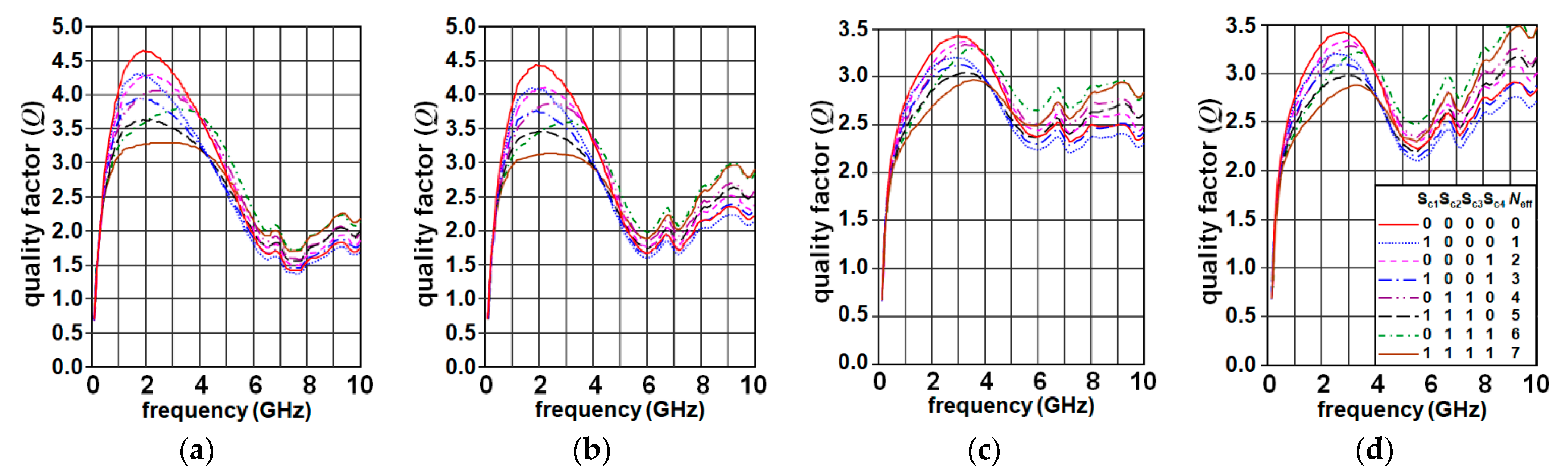
Figure 9a–d and Figure 10a–d show the simulated and measured inductances versus the frequencies of the proposed variable inductor in Figure 3b under different switch conditions for Sm1, Sm2, and Sc1–Sc4. The eight curves in each subfigure are similar to those in Figure 5, Figure 6, Figure 7 and Figure 8. Again, it can be seen that the inductances have coarse change steps by switching the status of Sm1 and Sm2 and fine change steps by switching the status of Sc1–Sc4. The simulated results are very similar to those shown in Figure 5a–d. As for the measured ones, the results are more similar to the simulated results at the frequency range between 1 GHz to 6 GHz for most cases, especially for the function of switch Sc1. At the 4 GHz frequency, the largest inductance is 575 pH, and the smallest inductance is 300 pH, corresponding to a change rate of the inductance of about 62.5%. Additionally, the fine step sizes of the switched inductances in Figure 10a–d are about 1% to 12.5% for most inductance range at 4 GHz. Again, the inductances show higher-order component behavior for frequencies larger than 6 GHz due to additional parasitic capacitance and loss from switches.
Figure 11a–d and Figure 12a–d show the corresponding simulated and measured Q factors versus the frequencies of the proposed inductor in Figure 3b, and the eight curves in each subfigure are under the same control status as those in Figure 9a–d and Figure 10a–d, except for the quantities are changed as the Q factors. For the simulated results, it can be seen that the peaks of the Q factors occur at the frequency range from 4.2 GHz to 6.0 GHz, depending on the status of the switches Sm1 and Sm2. There is a highest peak Q factor of 7.95 at 4.2 GHz for all switches being OFF, and there is a lowest peak Q factor of 2.6 at 7 GHz for all switches being ON. As for the measured cases, it can be seen that the peaks of the Q factors occur at the frequency range from 3.3 GHz to 4.5 GHz for most of the cases. Additionally, the peak values of Q factors are from 1.45 to 5.9 depending on the status of switches. The values of Q factors are varied from 1.45 to 5.65 at the frequency of 4 GHz. The loss on the switches seems to be worse than the case in Figure 3a for most cases except for the case in which all switches are in OFF status or only the switch Sc1 is ON.
In the design shown in Figure 3a, we aimed to combine two-turn secondary coupling coils with a one-turn coil for flexible tuning. We knew from Section 2.1 and Section 2.2 that the inductance changes of the two-turn secondary coupling coil of metal 1 and 2 are approximately 1.21 to 1.28 times that of the one-turn case of metal 1. Since each of the secondary coupling coils occupied one-quarter of the projection area of the main coil, no matter one turn or two turns, we expected the inductance change of m two-turn coils plus 1 one-turn coil will tend to the inductance change of (m+1) two-turn coils. However, the results shown in Figure 6a–d point to a different trend: the inductance change of m two-turn coils plus 1 one-turn coil tends to the inductance change of (m+1) two-turn coils at low frequency but tends to be m two-turn coils at a higher frequency. This may be due to the mutual coupling behavior difference between two-turn and one-turn secondary coupling coils, and it may also have the influence of the difference in the parasitic capacitance and resistance for the two cases. Nevertheless, this combination cannot provide uniform inductance change over a range of frequencies, and this may limit its application.
On the other hand, the combination of coils with different area sizes of two-turn secondary coupling coils can provide a relatively uniform inductance change over a range of frequencies. However, the step sizes of inductance changes become nonuniform between different Neff combinations for Sm1 or Sm2 that have ON status. This may be due to the current distribution of the main coil changed by switches Sm1 and Sm2, and the effective coupling areas are also changed from the original expected.
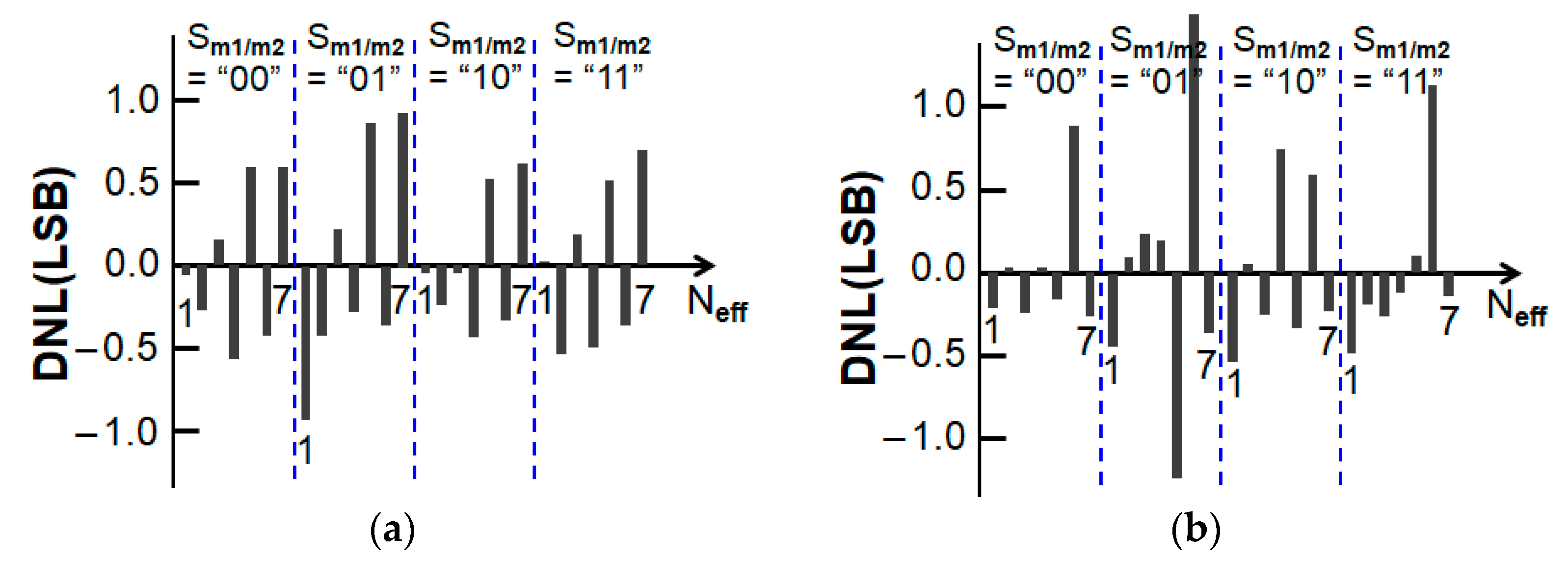
For investigating the step size of each switching status, we also calculated the differential nonlinearity (DNL) for each designed variable inductor from the measured data. The DNL is defined as
in which L(LSB) is defined as
i.e., the uniform inductance changing step size by switching Sc1–Sc4 for a certain Sm1 Sm2 status. The calculated DNL for the variable inductors shown in Figure 3a,b, respectively, are shown in Figure 13a,b, respectively. It can be seen that DNLs are within for most cases and the DNLs of the design in Figure 3b are averagely smaller than that of the design in Figure 3a except for some switching status. These results can be explained by the discussion provided in the previous two paragraphs.
From the results in previous work [9], we observed that the Q factor dropped significantly as the switches turned on, and this also happened in our cases. This effect is especially obvious in the results shown in Figure 12a–d. For the case that all switches are off, the Q factor has a peak value of 5.95 at 3.4 GHz. As Sc1 turns on, the peak of Q factor drops to about 5.5. For all other cases, Q factors do not exceed 3.85. The switches on the main coil paths will directly consume the power flowing in the path. The switches on the secondary coupling will decrease the magnetic energy store in the whole structure, and the parasitic resistance in the transistor also consumes power, which makes the Q factor even worse. Although a larger size of switch transistor may alleviate the loss, the parasitic capacitance will make the SRF significantly drop down. Besides the factors discussed above, another reason for the difference between the simulated results and the measured ones may be the NMOS model. Since we used the RF-NMOS, which has a fixed layout, and the parasitic effects are included in the device model, we did not include the layout of the NMOS at the EM stage. However, the metal layers of the NOMS transistors are located just beneath the designed coils, and there must be parasitic capacitance between them. The additional parasitic may further limit the bandwidth and Q factor of the designed variable inductor.
In our design, there are two sub-coils controlled by Sm1 and Sm2. This design is to prevent a large gap of inductance change. From the results shown above, the inductance change caused by the outer main coil controlled by Sm1 is relatively small, but it introduces significant parasitic capacitance and resistance. Therefore, the path controlled by Sm1 can be omitted to improve the bandwidth and the Q factor. Another strategy to improve the performance of the variable inductor may use the one-turn secondary coupling coils at the upper metal layers.
4. Conclusions
In this paper, we demonstrated a variable inductor design method using NMOS transistors as switches to change the main coil paths and secondary coupling coils. By changing the status of switches in both types of coils, large inductance tuning ranges with moderate step sizes are achieved. We successfully fabricated two chips of variable inductors. These variable inductors were designed and implemented in the 0.18 μm CMOS process technology. The proposed variable inductors can achieve 59.3% and 62.5%, respectively; inductance variation ranges and the fine step sizes of the switched inductances are about 0.5% to 6.1% for one design and 1% to 12.5% for the other for most inductance ranges at 4 GHz frequency. The Q factor property limits the application of the variable inductor, and it needs to be improved in future work. However, this variable inductor can still be used in some applications such as a wideband amplifier or wideband injection-locked frequency divider in which the Q factor may not be so critical.
Author Contributions
Conceptualization, Y.-C.C.; methodology, Y.-C.C.; software, J.-C.C.; validation, Y.-H.C.; formal analysis, Y.-C.C. and J.-C.C.; investigation, Y.-C.C.; data curation, Y.-C.C. and Y.-H.C.; writing—original draft preparation, Y.-C.C.; writing—review and editing, Y.-C.C. and J.-C.C.; visualization, Y.-C.C.; supervision, Y.-C.C. All authors have read and agreed to the published version of the manuscript.
Funding
This work was supported in part by the Ministry of Education, Taiwan, under the ATU plan and by the Ministry of Science and Technology, Taiwan, under Grant MOST 109-2221-E-005-064.
Acknowledgments
The authors would like to thank the Taiwan Semiconductor Research Institute (TSRI) in Hsinchu, Taiwan for the chip fabrication, measurement, and other technical supports. The authors would also like to thank Chiu-Hsiang Hsu, Ting-Yu Chen, Jin-Rong Chen, and Yu-Sheng Chen for their help in data preparation.
Conflicts of Interest
The authors declare no conflict of interest.
References
- Lubecke, V.M.; Barber, B.; Chan, E.; Lopez, D.; Gross, M.E.; Gammel, P. Self-assembling MEMS variable and fixed RF inductors. IEEE Trans. Microw. Theory Tech. 2001, 49, 45–50. [Google Scholar] [CrossRef]
- Yokoyama, Y.; Fukushige, T.; Hata, S.; Masu, K.; Shimokohbe, A. On-chip variable inductor using microelectro-mechanical systems technology. Jpn. J. Appl. Phys. 2003, 42, 2190–2192. [Google Scholar] [CrossRef]
- Chang, S.; Sivoththaman, S. A tunable RF MEMS inductor on silicon incorporating an amorphous silicon bimorph in a low-temperature process. IEEE Electron Device Lett. 2006, 27, 905–907. [Google Scholar] [CrossRef]
- Gmati, I.E.; Calmon, P.F.; Boukabache, A.; Pons, P.; Fulcrand, R.; Pinon, S.; Boussetta, H.; Kallala, M.A.; Besbes, K. Fabrication and evaluation of an on-chip liquid micro-variable inductor. J. Micromech. Microeng. 2011, 21, 1–9. [Google Scholar] [CrossRef]
- Li, Z.; Quintal, R. A dual-band CMOS front-end with two gain modes. IEEE J. Solid-State Circuits 2004, 39, 2069–2073. [Google Scholar]
- Park, P.; Kim, C.S.; Park, M.Y.; Kim, S.D.; Yu, H.K. Variable inductance multilayer inductor with MOSFET switch control. IEEE Electron Device Lett. 2004, 25, 144–146. [Google Scholar] [CrossRef]
- Sadhu, B.; Kim, J.; Harjani, R. A CMOS 3.3–8.4 GHz wide tuning range, low phase noise LC VCO. In Proceedings of the IEEE Custom Integrated Circuits Conference, San Jose, CA, USA, 13–16 September 2009; pp. 559–562. [Google Scholar]
- Demirkan, M.; Bruss, S.P.; Spencer, R.R. 11.8 GHz CMOS VCO with 62% tuning range using switched. In Proceedings of the IEEE Radio Frequency Integrated Circuits Symposium, Honolulu, HI, USA, 3–5 June 2007; pp. 401–404. [Google Scholar]
- Kossel, M.; Morf, T.; Buchmann, P.; Schmatz, M.L.; Menolfi, C.; Toifl, T. Switched inductor with wide tuning range and small inductance step sizes. IEEE Microw. Wireless Compon. Lett. 2009, 19, 515–517. [Google Scholar] [CrossRef]
- Demirkan, M.; Bruss, S.P.; Spencer, R.R. Design of wide tuning-range CMOS VCOs using switched coupled-inductors. IEEE J. Solid-State Circuits 2008, 43, 1156–1163. [Google Scholar] [CrossRef]
Figure 1.
Three-dimensional illustration of variable inductors by switching secondary coupling coil: (a) one-turn secondary coupling coil and (b) two-turn secondary coupling coil.
Figure 1.
Three-dimensional illustration of variable inductors by switching secondary coupling coil: (a) one-turn secondary coupling coil and (b) two-turn secondary coupling coil.

Figure 2.
Three-dimensional illustration of variable inductors by switching secondary coupling coil that occupies different percentages of one-quarter of the projection area of the main coil: (a) 25%, (b) 75%, (c) 100%, and (d) 150% (exceeding the projection area).
Figure 2.
Three-dimensional illustration of variable inductors by switching secondary coupling coil that occupies different percentages of one-quarter of the projection area of the main coil: (a) 25%, (b) 75%, (c) 100%, and (d) 150% (exceeding the projection area).

Figure 3.
Three-dimensional illustration of variable inductors by switching secondary coupling coil: (a) three one-quarter two-turn and one one-turn secondary coupling coils and (b) three one-quarter two-turn secondary coupling coils with one smaller two-turn coil.
Figure 3.
Three-dimensional illustration of variable inductors by switching secondary coupling coil: (a) three one-quarter two-turn and one one-turn secondary coupling coils and (b) three one-quarter two-turn secondary coupling coils with one smaller two-turn coil.

Figure 4.
Micrographs of variable inductors by switching secondary coupling coil: (a) three one-quarter two-turn and one one-turn secondary coupling coils as in Figure 3a and (b) three one-quarter two-turn secondary coupling coils with one smaller two-turn coil as in Figure 3b.

Figure 5.
Simulated inductances versus frequencies of the design in Figure 3a: (a) Sm1 Sm2 = “0 0”, (b) Sm1 Sm2 = “1 0”, (c) Sm1 Sm2 = “0 1”, and (d) Sm1 Sm2 = “1 1”.
Figure 5.
Simulated inductances versus frequencies of the design in Figure 3a: (a) Sm1 Sm2 = “0 0”, (b) Sm1 Sm2 = “1 0”, (c) Sm1 Sm2 = “0 1”, and (d) Sm1 Sm2 = “1 1”.

Figure 6.
Measured inductances versus frequencies of the design in Figure 3a: (a) Sm1 Sm2 = “0 0”, (b) Sm1 Sm2 = “1 0”, (c) Sm1 Sm2 = “0 1”, and (d) Sm1 Sm2 = “1 1”.
Figure 6.
Measured inductances versus frequencies of the design in Figure 3a: (a) Sm1 Sm2 = “0 0”, (b) Sm1 Sm2 = “1 0”, (c) Sm1 Sm2 = “0 1”, and (d) Sm1 Sm2 = “1 1”.

Figure 7.
Simulated Q factors versus frequencies of the design in Figure 3a: (a) Sm1 Sm2 = “0 0”, (b) Sm1 Sm2 = “1 0”, (c) Sm1 Sm2 = “0 1”, and (d) Sm1 Sm2 = “1 1”.
Figure 7.
Simulated Q factors versus frequencies of the design in Figure 3a: (a) Sm1 Sm2 = “0 0”, (b) Sm1 Sm2 = “1 0”, (c) Sm1 Sm2 = “0 1”, and (d) Sm1 Sm2 = “1 1”.

Figure 8.
Measured Q factors versus frequencies of the design in Figure 3a: (a) Sm1 Sm2 = “0 0”, (b) Sm1 Sm2 = “1 0”, (c) Sm1 Sm2 = “0 1”, and (d) Sm1 Sm2 = “1 1”.
Figure 8.
Measured Q factors versus frequencies of the design in Figure 3a: (a) Sm1 Sm2 = “0 0”, (b) Sm1 Sm2 = “1 0”, (c) Sm1 Sm2 = “0 1”, and (d) Sm1 Sm2 = “1 1”.

Figure 9.
Simulated inductances versus frequencies of the design in Figure 3b: (a) Sm1 Sm2 = “0 0”, (b) Sm1 Sm2 = “1 0”, (c) Sm1 Sm2 = “0 1”, and (d) Sm1 Sm2 = “1 1”.
Figure 9.
Simulated inductances versus frequencies of the design in Figure 3b: (a) Sm1 Sm2 = “0 0”, (b) Sm1 Sm2 = “1 0”, (c) Sm1 Sm2 = “0 1”, and (d) Sm1 Sm2 = “1 1”.

Figure 10.
Measured inductances versus frequencies of the design in Figure 3b: (a) Sm1 Sm2 = “0 0”, (b) Sm1 Sm2 = “1 0”, (c) Sm1 Sm2 = “0 1”, and (d) Sm1 Sm2 = “1 1”.
Figure 10.
Measured inductances versus frequencies of the design in Figure 3b: (a) Sm1 Sm2 = “0 0”, (b) Sm1 Sm2 = “1 0”, (c) Sm1 Sm2 = “0 1”, and (d) Sm1 Sm2 = “1 1”.

Figure 11.
Simulated Q factors versus frequencies of the design in Figure 3b: (a) Sm1 Sm2 = “0 0”, (b) Sm1 Sm2 = “1 0”, (c) Sm1 Sm2 = “0 1”, and (d) Sm1 Sm2 = “1 1”.
Figure 11.
Simulated Q factors versus frequencies of the design in Figure 3b: (a) Sm1 Sm2 = “0 0”, (b) Sm1 Sm2 = “1 0”, (c) Sm1 Sm2 = “0 1”, and (d) Sm1 Sm2 = “1 1”.

Figure 12.
Measured Q factors versus frequencies of the design in Figure 3b: (a) Sm1 Sm2 = “0 0”, (b) Sm1 Sm2 = “1 0”, (c) Sm1 Sm2 = “0 1”, and (d) Sm1 Sm2 = “1 1”.
Figure 12.
Measured Q factors versus frequencies of the design in Figure 3b: (a) Sm1 Sm2 = “0 0”, (b) Sm1 Sm2 = “1 0”, (c) Sm1 Sm2 = “0 1”, and (d) Sm1 Sm2 = “1 1”.

Figure 13.
Measured DNL of variable inductors for case: (a) three one-quarter two-turn and one one-turn secondary coupling coils, as in Figure 3a, and (b) three one-quarter two-turn secondary coupling coils with one smaller two-turn coil, as in Figure 3b.


Table 1.
Simulated inductance changes in percentage and Q factors for different metal layers of secondary coupling coil under short-circuited switch Sc.
Table 1.
Simulated inductance changes in percentage and Q factors for different metal layers of secondary coupling coil under short-circuited switch Sc.
| Metal 1 | Metal 2 | Metal 3 | Metal 4 | Metal 5 | |
|---|---|---|---|---|---|
| L @ 4 GHz | −5.07% | −5.59% | −6.23% | −6.99% | −7.87% |
| Q @ 4 GHz | 8.01 | 7.79 | 7.52 | 7.21 | 6.84 |
| L @ 8 GHz | −6.37% | −7.06% | −7.84% | −8.84% | −10.08% |
| Q @ 8 GHz | 11.87 | 11.55 | 11.14 | 10.64 | 10.01 |
| L @ 12 GHz | −6.97% | −7.25% | −8.64% | −9.74% | −11.22% |
| Q @ 12 GHz | 12.72 | 12.40 | 12.01 | 11.56 | 10.98 |
Table 2.
Simulated inductance changes in percentage and Q factors for different metal layers of two-turn secondary coupling coil under short-circuited switch Sc.
Table 2.
Simulated inductance changes in percentage and Q factors for different metal layers of two-turn secondary coupling coil under short-circuited switch Sc.
| Metal 1 and 2 | Metal 2 and 3 | Metal 3 and 4 | Metal 4 and 5 | |
|---|---|---|---|---|
| L @ 4 GHz | −6.12% | −6.84% | −7.54% | −8.63% |
| Q @ 4 GHz | 8.74 | 8.50 | 8.22 | 7.86 |
| L @ 8 GHz | −7.28% | −8.94% | −9.02% | −10.52% |
| Q @ 8 GHz | 13.35 | 13.0 | 12.59 | 12.00 |
| L @ 12 GHz | −8.98% | −10.26% | −11.05% | −13.22% |
| Q @ 12 GHz | 14.57 | 14.25 | 13.89 | 13.29 |
Table 3.
Simulated inductance changes in percentage and Q factors for different area percentages of one-turn secondary coupling coil under short-circuited switch Sc.
Table 3.
Simulated inductance changes in percentage and Q factors for different area percentages of one-turn secondary coupling coil under short-circuited switch Sc.
| 25% | 50% | 75% | 100% | 150% | |
|---|---|---|---|---|---|
| L @ 4 GHz | −0.27% | −1.14% | −3.25% | −5.07% | −1.73% |
| Q @ 4 GHz | 10.62 | 9.83 | 8.77 | 8.01 | 9.75 |
| L @ 8 GHz | −0.36% | −1.48% | −4.12% | −6.37% | −2.15% |
| Q @ 8 GHz | 15.17 | 14.38 | 12.80 | 11.87 | 14.06 |
| L @ 12 GHz | −0.42% | −1.62% | −4.47% | −6.97% | −2.32% |
| Q @ 12 GHz | 14.77 | 14.25 | 13.13 | 12.72 | 14.01 |
Table 4.
Simulated inductance changes in percentage and Q factors for different widths of NMOS transistors as the switch of two-turn secondary coupling coil.
Table 4.
Simulated inductance changes in percentage and Q factors for different widths of NMOS transistors as the switch of two-turn secondary coupling coil.
| W | 30 μm | 60 μm | 120 μm | 180 μm | 240 μm | 300 μm |
|---|---|---|---|---|---|---|
| L @ 4 GHz | −1.63% | −3.20% | −4.61% | −5.25% | −5.60% | −5.85% |
| Q @ 4 GHz | 8.04 | 8.01 | 8.04 | 8.16 | 8.26 | 8.32 |
| L @ 8 GHz | −4.36% | −5.95% | −7.14% | −7.95% | −8.75% | −9.60% |
| Q @ 8 GHz | 10.42 | 11.06 | 11.93 | 12.34 | 12.57 | 12.70 |
| L @ 12 GHz | −6.89% | −8.34% | −10.90% | −13.92% | −14.88% | −3.81% |
| Q @ 12 GHz | 11.13 | 12.28 | 13.19 | 13.54 | 13.73 | 13.84 |
Publisher’s Note: MDPI stays neutral with regard to jurisdictional claims in published maps and institutional affiliations. |
© 2021 by the authors. Licensee MDPI, Basel, Switzerland. This article is an open access article distributed under the terms and conditions of the Creative Commons Attribution (CC BY) license (https://creativecommons.org/licenses/by/4.0/).
Share and Cite
MDPI and ACS Style
Chiang, Y.-C.; Chen, J.-C.; Chang, Y.-H. A Study on the Variable Inductor Design by Switching the Main Paths and the Coupling Coils. Electronics 2021, 10, 1856. https://0-doi-org.brum.beds.ac.uk/10.3390/electronics10151856
AMA Style
Chiang Y-C, Chen J-C, Chang Y-H. A Study on the Variable Inductor Design by Switching the Main Paths and the Coupling Coils. Electronics. 2021; 10(15):1856. https://0-doi-org.brum.beds.ac.uk/10.3390/electronics10151856
Chicago/Turabian StyleChiang, Yen-Chung, Juo-Chen Chen, and Yu-Hsin Chang. 2021. "A Study on the Variable Inductor Design by Switching the Main Paths and the Coupling Coils" Electronics 10, no. 15: 1856. https://0-doi-org.brum.beds.ac.uk/10.3390/electronics10151856
Note that from the first issue of 2016, this journal uses article numbers instead of page numbers. See further details here.