
Terahertz High-Q Absorber Based on Holes Array Perforated into a Metallic Slab


1
Department of Electrical Engineering, Sirjan University of Technology, Sirjan 7813733385, Iran
2
School of Engineering, RMIT University, Melbourne, VIC 3003, Australia
*
Author to whom correspondence should be addressed.
Electronics 2021, 10(15), 1860; https://0-doi-org.brum.beds.ac.uk/10.3390/electronics10151860
Submission received: 2 June 2021
/
Revised: 25 July 2021
/
Accepted: 30 July 2021
/
Published: 2 August 2021
(This article belongs to the Special Issue Microwave Devices Design and Application)
Abstract
:In this paper, we theoretically analyze and design a dual-narrowband terahertz (THz) absorber based on a hole array drilled into a metallic slab. A very high-quality factor (Q) is achieved at both of the resonance frequencies. A circuit model-based approach is developed for the analysis and design of the proposed absorber. The absorption peaks occur at 2.46 and 3.75 THz frequencies with 98% and 96% absorptions at normal incidence, respectively. The achieved quality factors are 149 and 144, at 50% absorbance for the two absorption bands, respectively.
1. Introduction
For the first time, high-transmission peaks through arrays of subwavelength apertures have been investigated using near-field scanning optical microscopy (NSOM) by Betzig et al. [1], without presenting an analytical explanation on the operation principle. Then, both theoretical and experimental results for understanding the physics involved in the Extraordinary Optical Transmission (EOT) in nano-holes arrays have been presented by Ebbesen et al. [2]. Extraordinary Optical Transmission (EOT) appears as a strong narrowband peak in the transmission spectrum and has been applied in different optical devices [3,4,5,6,7,8,9,10,11,12,13,14,15,16,17,18,19,20,21,22,23,24]. Surface Plasmon Polaritons (SPPs) were considered as the main reason for this phenomenon [9]. Metals show negative permittivity at high frequencies, and therefore can support SPs [10]. However, the observation of this phenomenon at lower frequencies undermines this hypothesis [11]. The localization of a THz surface wave is different from the SPPs in the visible region. At THz frequencies, the majority of metals show almost perfect conductor behavior; thus, the THz surface wave is less localized close to the metal surface. This resonance-based transmission phenomenon in the holes array is due to the resonance coupling between the incident electromagnetic wave and the surface waves on the metal surface through the periodic structure [5]. Based on circuit models, this was shown to be the result of high-order diffracted modes related to the inductive or capacitive admittance at the interface between the holes array and the surrounding homogeneous medium. These modes are evanescent in the subwavelength regime and store electromagnetic energy near the interface. Capacitive admittance is due to the electrical energy of TM-polarized diffracted modes, whereas the inductive admittance is due to the magnetic energy stored in the TE diffracted modes [14,15,16,17,18,19,20,21,22,23].
A conventional approach to control the reflections of electromagnetic waves is the Salisbury screen, which includes a lossy screen placed a quarter wavelength above a conductor surface. These screens have been applied in the design of the absorbers [24,25,26,27]. Recently, the absorbers based on metamaterial attracted the interest of researchers. The majority of the metamaterial absorbers in the literature are made with three layers as a combination of patterned layers, which act as electric resonators, a dielectric substrate, and a metallic reflector at the bottom side. Electromagnetic perfect absorbers have been investigated for various applications including wireless communications, thermal emitters, sensors, photodetectors and photovoltaic structures [28,29,30,31,32,33]. Based on the targeted applications, narrowband or broadband absorbers were investigated. Designing a narrowband absorber with a high-quality factor has always been a challenge [28,29,30,31,32,33,34,35,36,37,38,39,40,41]. Narrowband absorbers can be used to implement microbolometers for terahertz imaging systems [28]. In addition, high-sensitivity narrowband resonance can be used for refractive index sensing applications [29,30,31,32,33].
Single narrow band absorbers have been reported in [32,33,34]. The absorber in [32] consists of a GaAs cross-shaped patch deposited on copper and dielectric substrate terminated by copper, which provides a single absorption band at 2.44 THz with a quality factor of 637. The structure presented in [33] consisting of a 1D periodical cavity array in the gold plate and slots on the top of the cavities. A strong resonance occurs at 1.593 THz with nearly perfect absorption and a quality factor of 1028. A narrowband absorber consisting of two metallic layers as an array of patches and arrays of meshes separated by a dielectric spacer placed on a grounded substrate has been realized in [34]. The perfect absorption band occurs at 0.5 THz with a quality factor of 32. In [35], a dual-band absorber composed of a metallic cross-shaped structure deposited on the grounded substrate has been investigated. Two discrete absorption peaks at 1.46 THz and 2.89 THz were implemented with 95.31% and 92.92% absorption, respectively. The quality factor of the first and second absorption bands are 7 and 48.2, respectively.
Recently, narrow-band absorbers with small dimensions and high-quality factors based on graphene metamaterials have received great attention [36,37,38,39]. The absorber presented in [36] is made of two stacked graphene disk arrays. The absorption bands appear at 3 THz and 5 THz with a quality factor of 22 and 41, respectively. In [37], a layer of graphene disks array has been used to design a dual narrowband absorber at 1.9 and 5 THz frequencies with 16 and 40 quality factors, respectively. However, due to the challenges associated with tuning the graphene properties and biasing of the graphene layers, structures based on metallic materials are still prevalent.
The phenomenon of (EOT) through subwavelength holes array perforated inside a metallic film [40,41,42,43,44,45] has been crucial for the development of plasmonic devices. Unlike the apertures inside the zero-thickness screen creating a transmission peak, the apertures inside the screen with finite thickness lead to two peaks in the transmission spectra because of the reactive energy stored inside the holes [15]. Therefore, these structures can be used in applications, where two resonant bands are required, while most of the other two-dimensional metasurfaces, such as metallic patches over a grounded dielectric slab, intrinsically create a single resonant band [46,47,48]. However, a typical disadvantage of EOT hole arrays compared to other two-dimensional metasurfaces is the relatively large number of holes necessary to get the resonances with a high peak [43]. In addition, the stability with respect to the incident angle for transmission spectra of the EOT holes array is smaller than the metallic patches specifically for the TM polarization [40,43]. Here, we use the resonance properties of the hole array to realize a very narrow dual-band absorber at THz frequencies.
In this paper, a very narrowband absorber with dual absorption bands is theoretically designed and analyzed based on a hole array. The absorption bands occur at 2.46 and 3.75 THz with quality factors of 149 and 144, respectively. An accurate circuit model is developed to study the resonance behavior of the structure when the holes are drilled into the perfect electric conducting (PEC) slab. The loss due to the finite conductivity of the metallic slab can help to achieve near-perfect absorption.
The rest of the paper is organized as follows: Section 2 describes the proposed structure to realize the very narrow absorption bands. A circuit model-based analytical method is presented to model the narrowband absorber in this section. Results and discussions are presented in Section 3. Finally, Section 4 presents the main conclusions.
2. Design of the Dual-Narrow Band Absorber
The majority of the metamaterial absorbers are made by a combination of patterned layers, which act as electric resonators and a dielectric substrate that is terminated by a metallic back reflector. Various multiband absorbers were realized by using resonators of different sizes and shapes or in multi-layer structures, where the multi-band response is formed by resonances induced by each individual resonator array. The holes array is known as EOT structures. According to the circuit model and the mechanism presented in [23], this structure leads to two resonances. Here, the metallic holes array is employed on top of a dielectric slab terminated with a back metallic reflector to realize a dual-band absorber. The loss associated with the dielectric layer and the finite conductivity of metallic slab at terahertz frequencies produce near-perfect absorption at the resonance frequencies of the absorber.
2.1. Structure
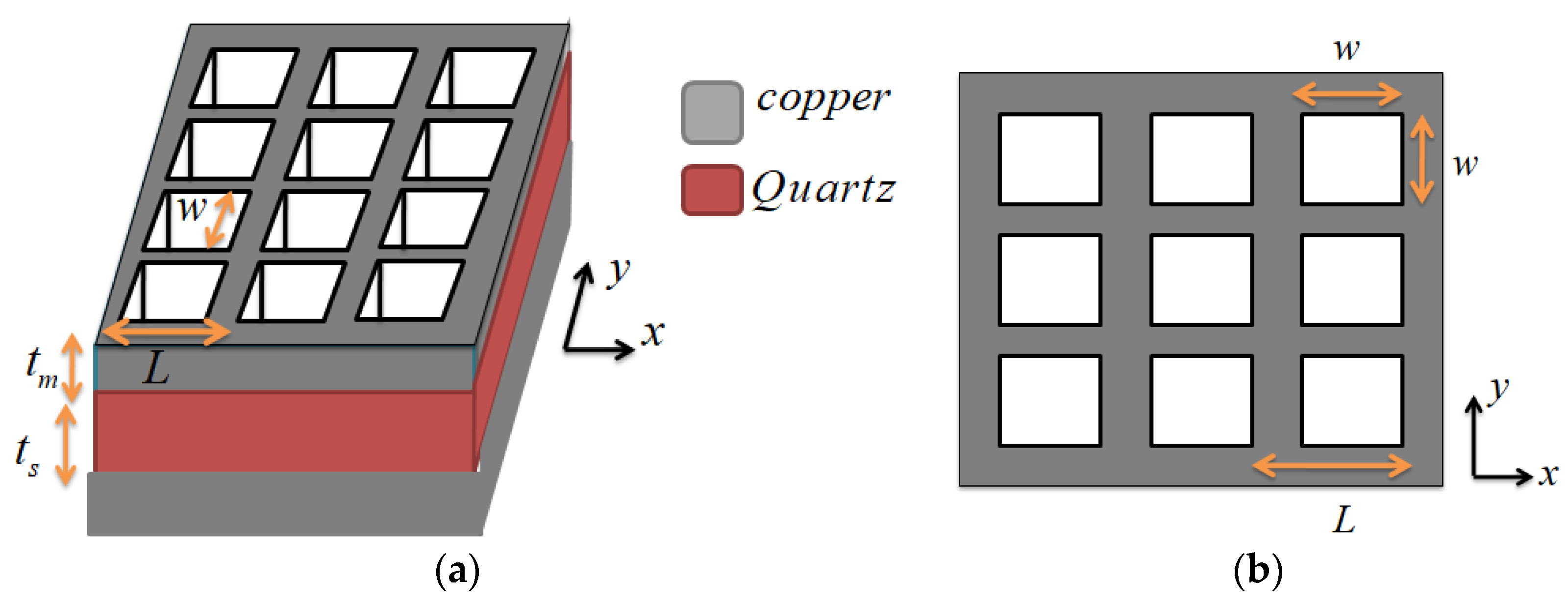
As shown in Figure 1, the absorber is composed of three layers consisting of a patterned array of holes drilled into a metallic slab, a dielectric slab of thickness ts, and a metal reflector. The periodicity in both x- and y-directions is L. The width and depth of holes are considered as w and tm, respectively. The dielectric spacer is Quartz with a relative permittivity of 3.8(1 − j0.0015). The metallic layer is made of copper. The absorption coefficient of the absorber is determined by , where and represent the frequency-dependent transmission and reflection coefficients, respectively. In order to inhibit transmission, the metallic ground plane should be much thicker than the skin depth in the working frequency of the absorber. To achieve perfect absorption, the reflection coefficient should be near zero, which is realized by the impedance matching condition.
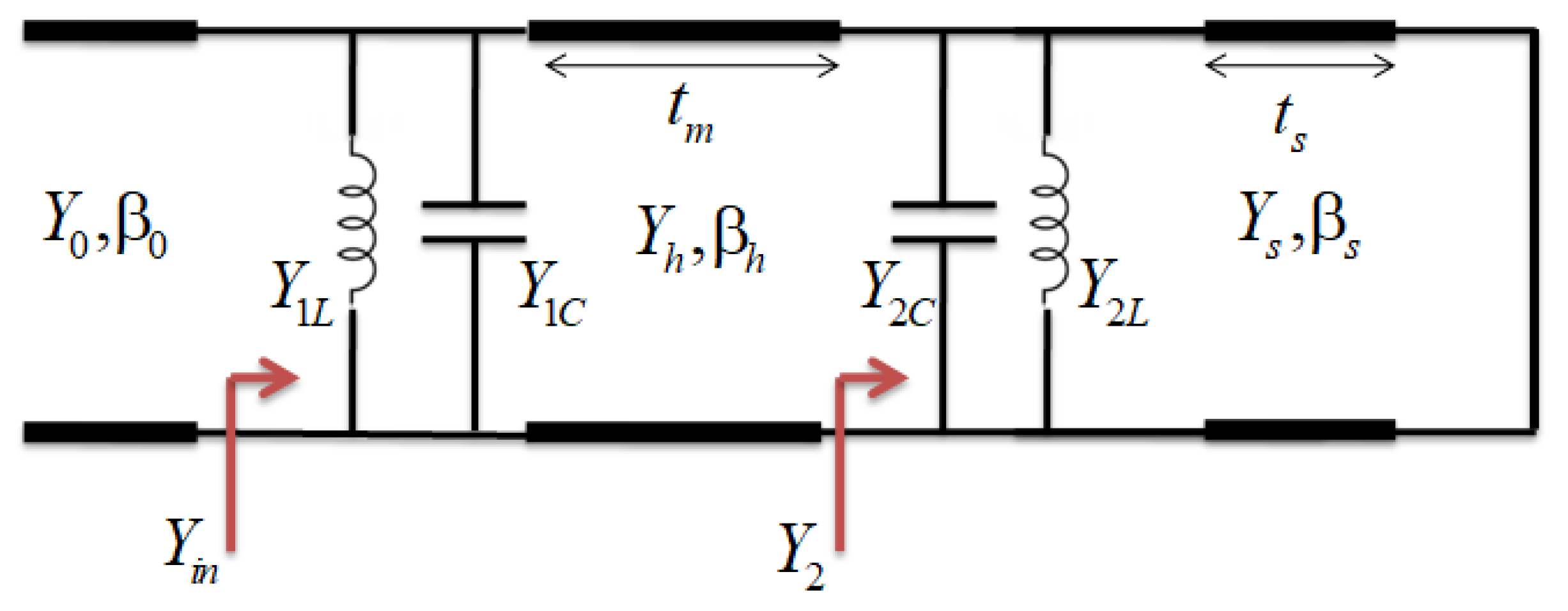
2.2. The Equivalent Circuit Model
In order to have a better understanding of the structure and its operation principle, circuit analysis of the proposed absorber is investigated in this section [23,48]. In the analysis, we suppose that the holes array is drilled into a PEC film. In the circuit-based analysis, we utilize the circuit model presented in [23], where the holes were perforated into a semi-infinite conductor. An incident plane wave impinges from the free space into the holes array. The electromagnetic field in the semi-infinite homogeneous region above the perforated metallic structure was decomposed in terms of the incident plane wave and all reflected diffraction orders as a combination of TE and TM modes. The fundamental mode () was considered inside the holes. Using the boundary conditions at the interface between free space and the hole array medium, the zeroth-order reflection coefficients for the TE and TM waves were driven [23]. There are couplings between the TE and TM polarizations such that the TM incident wave can generate reflected TE waves and vice versa. Thus, in order to introduce a simple circuit model, the focus of our analysis is only the normal incidence on the structure, where the structure is polarization-insensitive. Finally, with limiting the analysis to the case, where only the TM normal incident wave is impinging the structure, the zeroth-order reflected wave coefficient is calculated as:
This is equivalent to the reflection coefficient at the interface between two transmission lines with characteristic admittances of Y0 and Yh combined with a surface admittance as two shunt admittances (YC, and YL) at the interface between the two transmission lines. The inductive or capacitive admittance at the interface between the holes array and the surrounding homogeneous medium results from the high-order diffracted modes, which are evanescent in the subwavelength regime, and store electric and magnetic energy near the interface. Capacitive admittance is due to the electrical energy of TM-polarized diffracted modes, whereas inductive admittance results from the magnetic energy stored in TE diffracted modes. Supposing that the holes array has a finite thickness, the transmission-line model shown in Figure 2 can be used for modeling. In Figure 2, the surface shunt admittances are obtained as:
where
are the partial wave admittances in free space and substrate homogeneous regions for the TE and TM polarizations, respectively with i =1,2.
where ε1 = 1 and ε2 = 3.8(1 −j0.0015) are the relative permittivities of the free space and the quartz (substrate slab). For the normal incident, kx = ky = 0.
In subwavelength regime, since the period of the structure is assumed to be much smaller than the incident wavelength, only the first diffraction order propagates, while the higher orders are evanescent, so that is imaginary for these orders. The quantity
is the overlap integral between the diffraction order specified by m and n according to (1), and the dominant mode inside the holes.
In the equivalent circuit model (Figure 2), and are the propagation constant and the admittance of transmission line corresponding to the substrate layer, respectively, where is the free-space impedance and (c is the speed of light in vacuum) is the free space wave number. A sufficiently thick layer of metal is required for the bottom ground plane such that a perfect electric conductor (PEC) approximation is true. Therefore, the metallic back reflector can be approximately considered as a short circuit. The propagation constant and characteristic admittance of the transmission line corresponding to holes array can be calculated as:
where and are the propagation constant and admittance of the fundamental mode () inside the holes, respectively. can be calculated by replacing in (5).
The input admittance of the proposed structure is obtained as:
According to the discussions and explanations presented in [23], for the hole arrays with very thin depth, the resonance frequency can be estimated by neglecting the effect of the intermediate transmission line equivalent to the holes array. The resonance occurs, where the imaginary part of the surface admittance modeled as shunt admittances in the circuit model are zero. In the case of holes with finite depth, the inductive effect of the intermediate transmission line equivalent to the hole must be considered, which results in two resonances [23].
3. Discussions and Results
In this section, we design the parameters of the structure to realize a dual-narrowband absorber. In order to achieve a narrowband absorber, the structure parameters are selected as: , , and . The metallic films are modeled with a Drude function, which models them as a complex permittivity obtained from the Drude model calculated by:
where is the permittivity at infinite frequency, is angular frequency, is plasma frequency of the free electron gas, and is characteristic collision frequency. For copper, the Drude model is developed using , [49]. The dielectric spacer is Quartz with a relative permittivity of 3.8(1 − j0.0015).
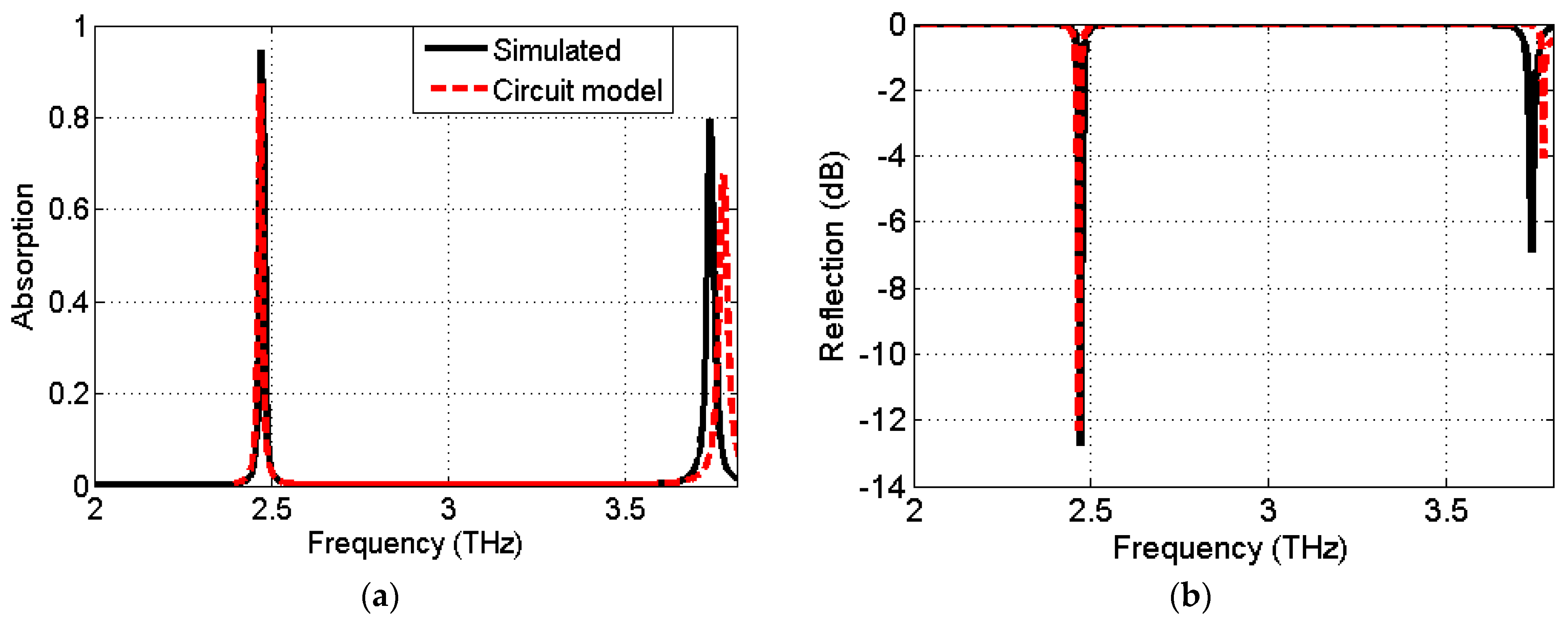
High-Frequency Structure Simulator (HFSS) software-based finite element method (FEM) solver is used to simulate the absorber. The unit cell is surrounded by a periodic boundary condition (Master and Slave boundary conditions) along x- and y-directions, and the Floquet port at the z-direction. Tetrahedral mesh has been considered for full-wave simulations. The initial mesh is generated by default. HFSS then uses auto adaptive meshing to generate the final mesh. In each pass, HFSS selects smaller meshes to achieve convergence. Iterative algorithm solves fields and refines mesh until user-defined convergence threshold value is reached. The maximum number of passes is selected to be 10. The maximum number of passes is the maximum number of mesh refinement cycles. This value is a stopping criterion for the adaptive solution. At the first step, we compare the result obtained from the full-wave simulations to the ones obtained from the circuit model as plotted in Figure 3. In the circuit model, the holes are supposed to be drilled out of the PEC slab. As seen, two absorption bands can be achieved using this structure. The results are in good agreement. The loss due to the finite conductivity of the metallic layer can enhance the absorption values, especially at the second band. Figure 4a shows the results after using copper as a top and bottom metallic layer.
Figure 4a shows that two absorption bands with over 96% absorption can be identified at 2.46 THz and 3.75 THz after using copper as the metallization layer. The resonance bands are obtained due to the resonant coupling of the incident electromagnetic wave with the surface waves excited on the metallic surface through the periodic structure. In addition, the loss contribution from the dielectric spacer in the proposed absorber is studied as shown in Figure 4b. As illustrated, there is no obvious difference in lower frequency region by having a lossy or loss-free dielectric spacer. However, in the higher frequency region, the absorption peak of the structure with lossy dielectric has slightly higher absorption level compared with the one with loss-free dielectric.
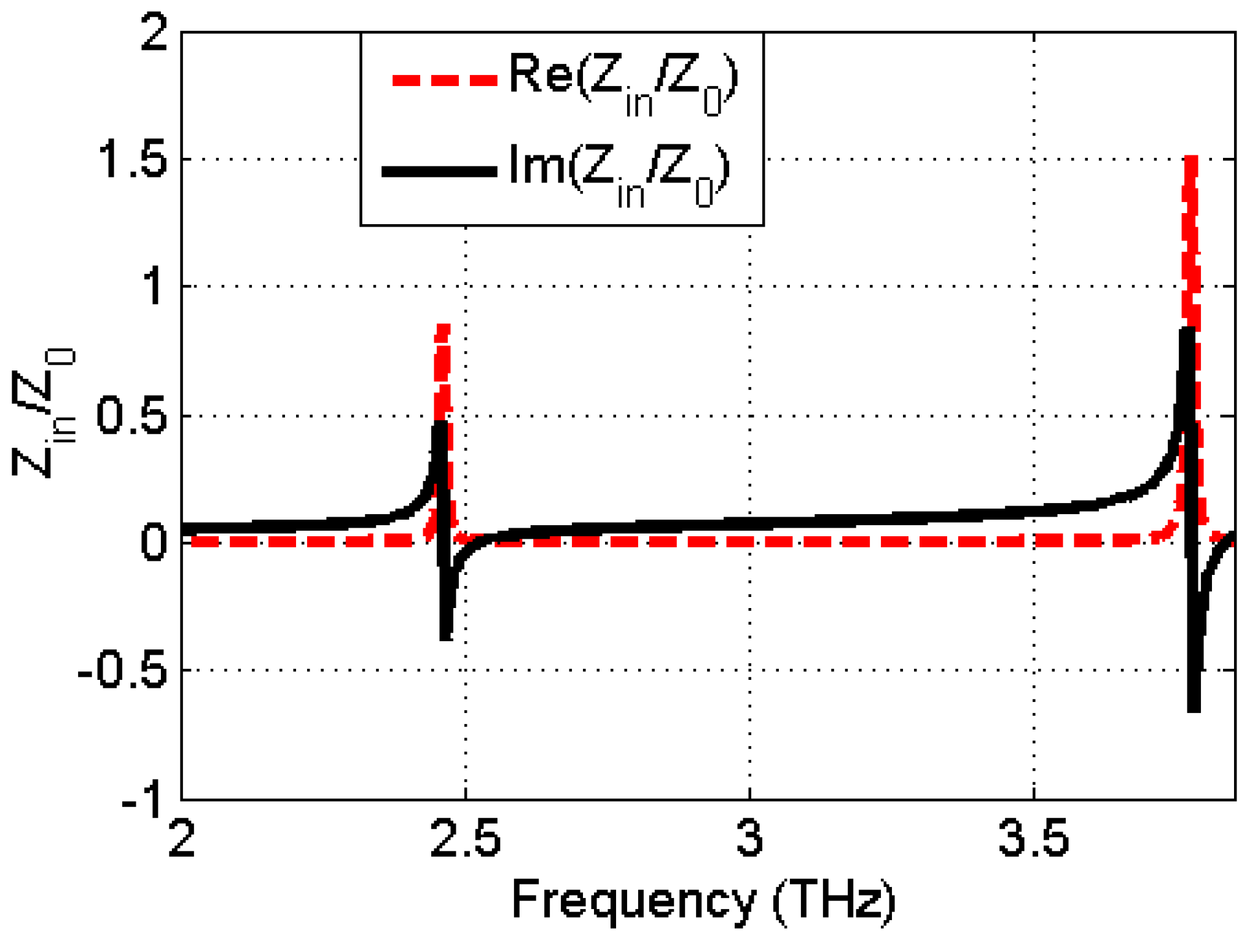
Random surface roughness and surface distortions occur inevitably because of various material processing and fabrication techniques which might affect the absorption peak [50,51]. Based on our previous experiences [34], these factors would not have a significant effect on the performance if an accurate fabrication process is used. The normalized input impedance for the proposed structure is plotted in Figure 5. As observed, there are two resonance frequencies, where the imaginary part of the normalized impedance is near zero and its real part is close to 1. Therefore, the impedance matching condition leading to high absorption is achieved at two bands.
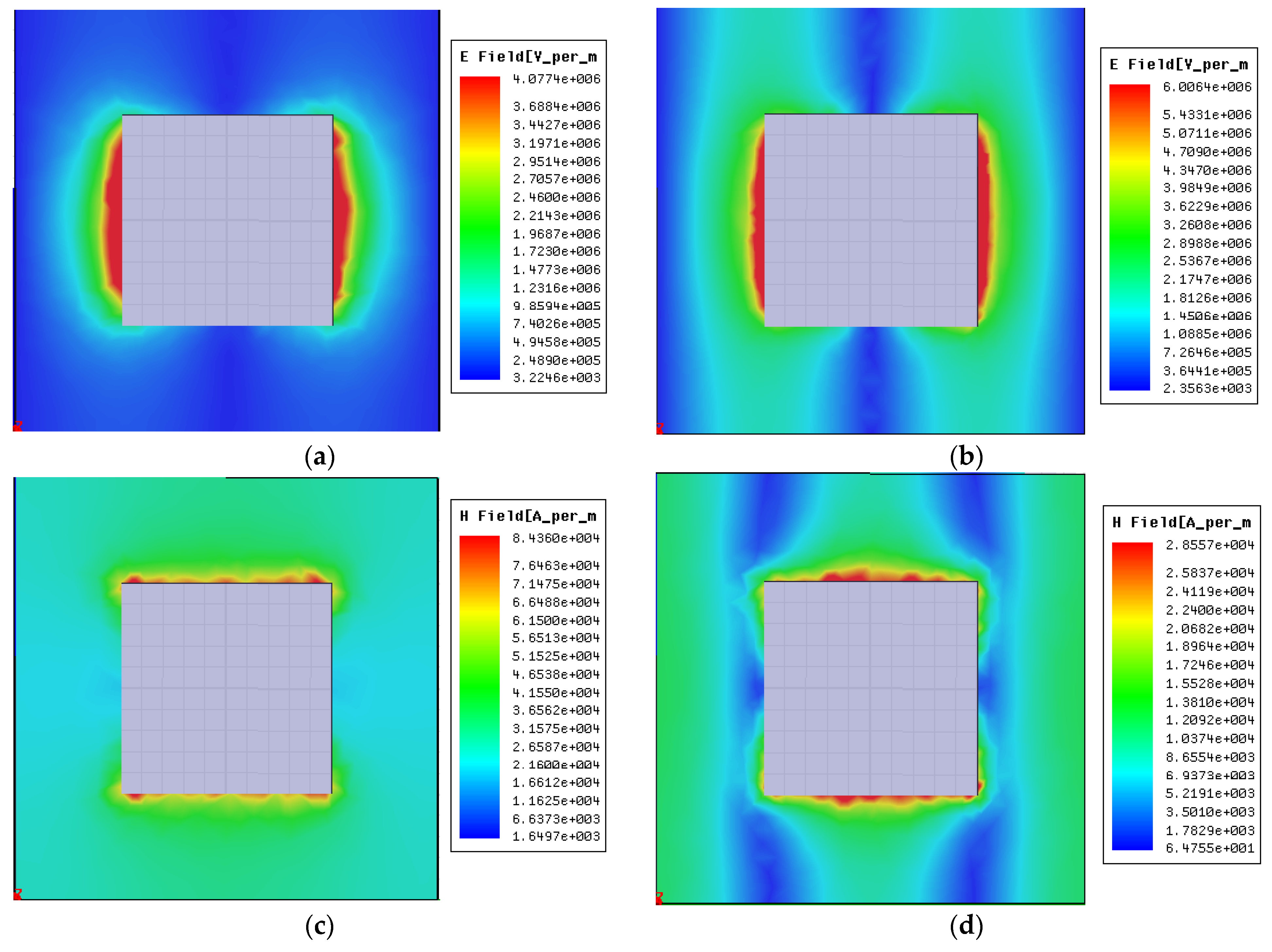
Figure 6 shows the distribution of the electric and magnetic fields at the first and second bands for a TM incident wave. Based on Figure 6a,b, there is a strong concentration of electric field in the right and left edge areas of holes implementing the capacitive nature of the surface admittance. Moreover, according to Figure 6c,d, there is a dense distribution of the magnetic field in the top and bottom edge areas of the holes, which verifies the existence of inductive properties at the interface. Now, we investigate the effect of geometrical parameters on absorption spectra.
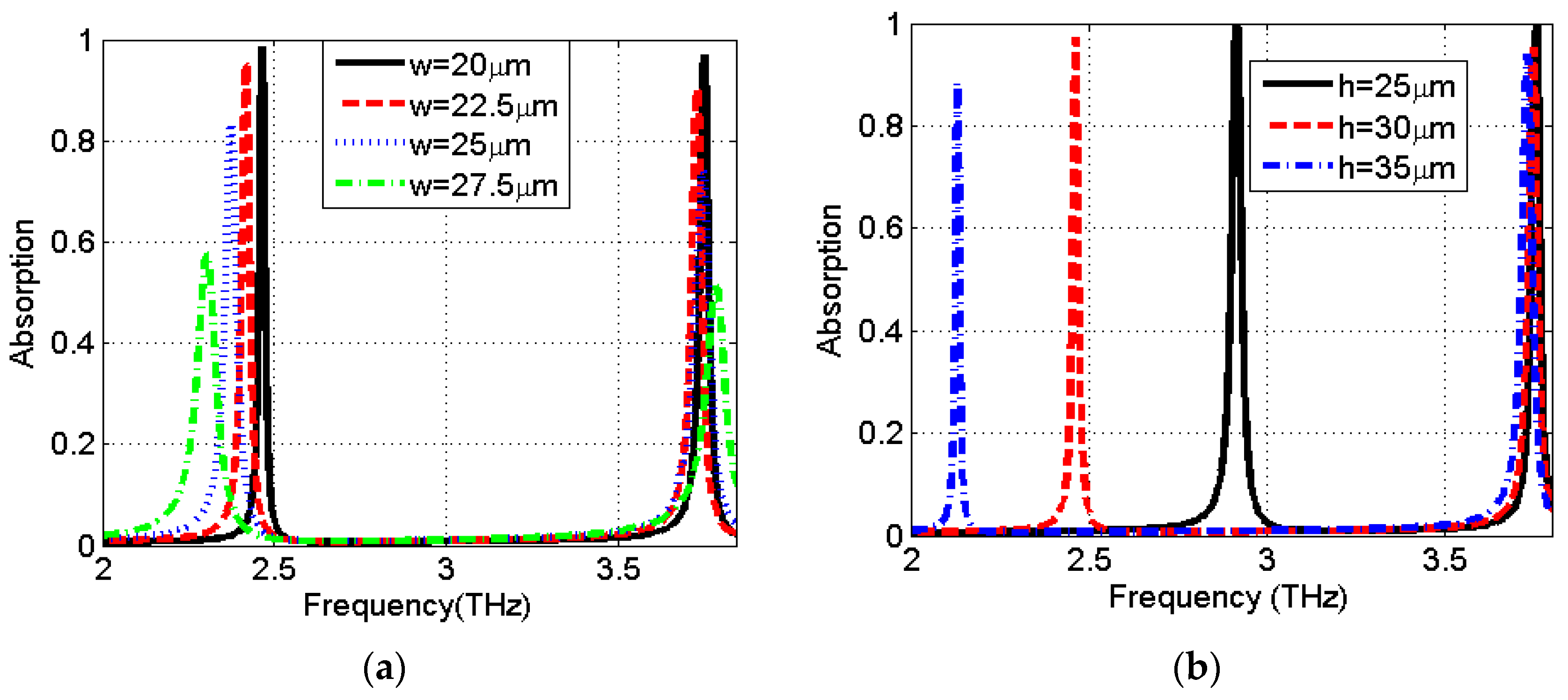
Figure 7a,b show the absorption spectra for various widths of holes and thickness of dielectric substrate, respectively. As shown in Figure 7a, increasing the width of holes reduces the value of the absorption and shifts the resonance frequencies downwards. In addition, by changing the thickness of the dielectric substrate, the absorption bands can be tuned to different frequencies as plotted in Figure 7b, where there is a significant shift in the first resonance, while the shift of the second resonance is negligible.
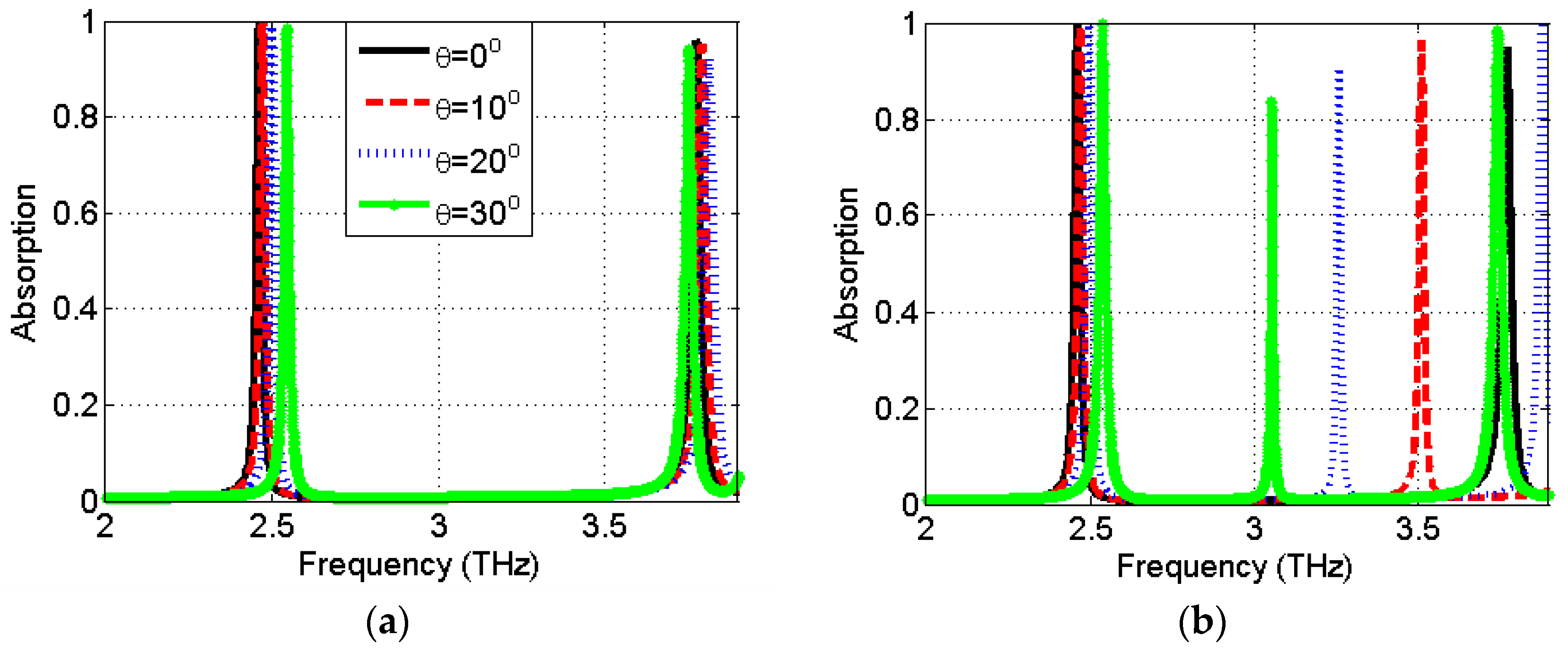
In the following, the dependence of the proposed structure to the incidence angle is investigated. As illustrated in Figure 8a, the absorption bands with absorption above 90% can be observed while the incident angle up to 30 degrees for the TE polarization. Small shifts can be absorbed at both the resonant frequencies via incident angle changes for the TE polarization. Therefore, the stability with respect to TE polarization up to 30° can be observed similar to the previous experimental works for aperture arrays [40]. In addition, more than 90% absorption is achieved at the first resonant band for various incident angles in TM polarization. However, other resonant bands are observed for TM polarization at higher incidence angles. The excitation of higher order modes for TM polarization by increasing incident angle has been experimentally reported in EOT structures too [45].
A comparison of the proposed narrow band absorber with some of the recently reported narrowband absorbers at THz frequencies is summarized in Table 1. As seen in the table, the proposed absorber results in the most impressive quality factor in comparison with the rest of the designs [35,36,37]. The quality factor (Q) is defined as Q = f0/FWHM [32,33,34], where FWHM is the full width at half maximum and f0 is the central frequency of each band. Furthermore, comparison between the proposed dual-band absorber to the structure presented in [35], which is based on metallic patterned layers shows that the structure presented in this paper has a smaller unit cell size. For the structure proposed in [35], the size of the unit cell and the thickness are and , respectively. The unit cell size and the thickness of the presented design are and , respectively. Although the structures presented in [36,37] have smaller unit cell sizes, these structures are based on graphene layers and the fabrication of graphenelayers, and their bias is very challenging.
Effect of Gaussian Beam
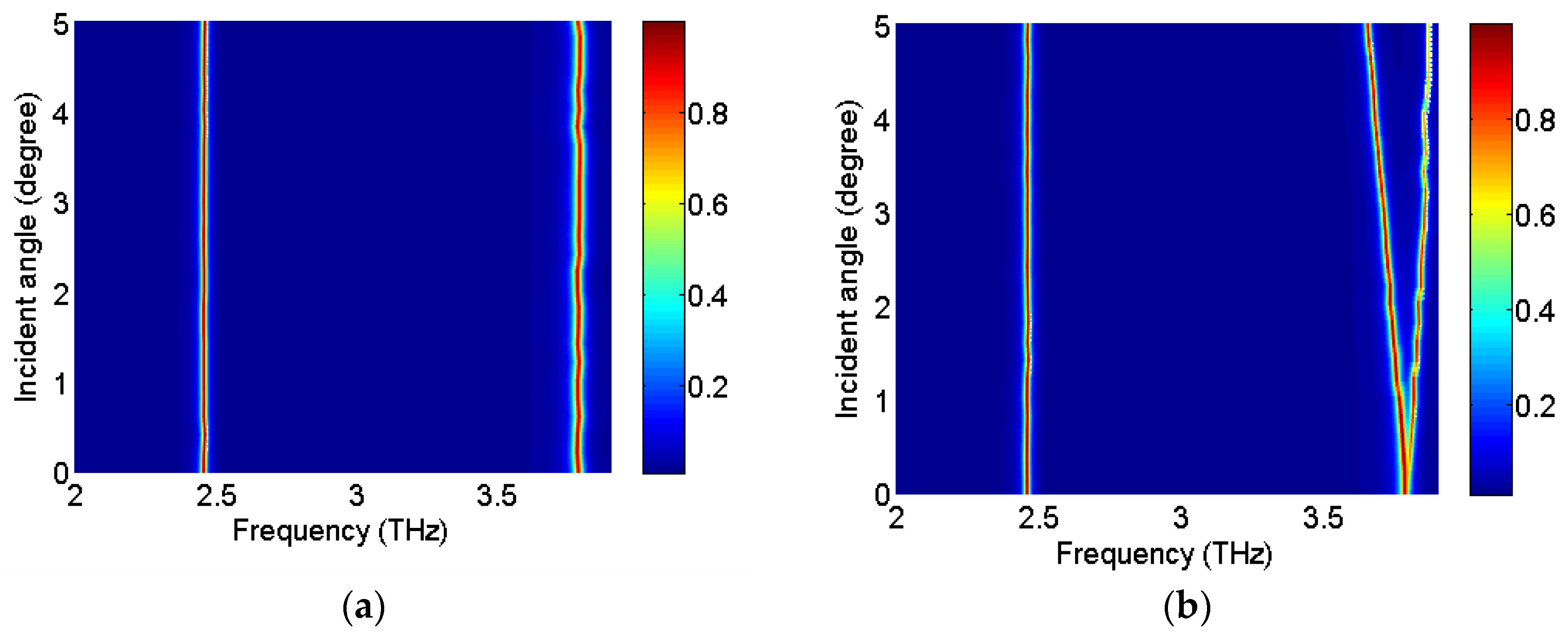
Here we study the influence of Gaussian distribution of the terahertz incident beam. Although lenses and mirrors are used in majority of the terahertz measurement setups to generate collimated beams, in many cases, there is some residual divergence that is not negligible in real measurements [40,41,42,43]. In fact, Gaussian beams can be modeled by an infinite number of plane waves with different angular wave vectors. Thus, it is expected that for small sizes of Gaussian beams, the absorption response diverges from response under normally incident plane wave. This happens since even on a normally incident Gaussian beam, a significant part of the beam obliquely impinges on the absorber surface [43]. In order to study this effect, we follow the procedure explained in [43]. A unit cell of absorber is simulated under plane-wave excitation (the absorber is infinite along x and y), where the incidence angle is swept within 0–5° for taking into account the obliquely incident portion of the Gaussian beam. The results are presented in Figure 9 for both of the TE and TM polarizations. Based on the results in Figure 9, it is expected that a frequency splitting happens for the second absorption band in the TM polarization with a decrease in the absorption peak.
Based on the findings in [43,44,45], the leaky wave would be excited on the surface of the metallic hole array, especially if the excitation is not a plane wave. This leaky surface wave travels a high number of unit cells before its power becomes negligible. In fact, the minimum number of unit cells required to achieve optimum performance (similar to an infinite array) depends on the spot area of the excitation electromagnetic beam (πϖ02, ϖ0 is the beam waist). Investigations in [43] on the hole arrays proved that an array with at least 10 times larger area than the beam spot offers maximum transmission at the resonance frequency.
4. Conclusions
In this paper, we investigated a dual-narrowband absorber based on the holes array drilled into a metallic slab deposited on a grounded dielectric spacer. We used an equivalent circuit model to analyze the structure and verified the results using a circuit model analysis. Based on the equivalent circuit model, the resonance modes are due to the shunt inductive and capacitive admittances at the interface between the hole array and the surrounding homogeneous medium associated with high-order diffracted modes, and the inductive effect of the intermediate transmission corresponding to the fundamental mode () inside the holes. The diffracted modes are evanescent in the subwavelength regime, and store electric and magnetic energy near the interface corresponding to the TM and TE-polarized diffracted modes, respectively. The proposed dual narrowband absorber offers higher quality factor absorption in comparison with the state-of-art dual narrowband absorbers.
Author Contributions
Design, Simulation, Writing-Original draft preparation, S.B.-P.; Data analysis, Conceptualization, Reviewing and Editing, A.E. All authors have read and agreed to the published version of the manuscript.
Funding
This research received no external funding.
Conflicts of Interest
The authors declare no conflict of interest.
References
- Betzig, E.; Lewis, A.; Harootunian, A.; Isaacson, M.; Kratschmer, E. Near-Field Scanning Optical Microscopy (NSOM) development and biophysical applications. Biophys. J. 1986, 49, 269–279. [Google Scholar] [CrossRef] [Green Version]
- Ebbesen, T.W.; Lezec, H.J.; Ghaemi, H.F.; Thio, T.; Wolff, P.A. Extraordinary optical transmission through sub-wavelength hole arrays. Nature 1998, 391, 667–669. [Google Scholar] [CrossRef]
- Cao, H.; Nahata, A. Influence of aperture shape on the transmission properties of a periodic array of subwavelength apertures. Opt. Exp. 2004, 12, 3664–3673. [Google Scholar] [CrossRef] [PubMed]
- Cao, H.; Nahata, A. Resonantly enhanced transmission of terahertz radiation through a periodic array of subwavelength apertures. Opt. Exp. 2004, 12, 1004–1010. [Google Scholar] [CrossRef]
- Miyamaru, F.; Hayashi, S.; Otani, C.; Kawase, K. Terahertz surface-wave resonant sensor with a metal hole array. Opt. Lett. 2006, 31, 1118–1120. [Google Scholar] [CrossRef]
- Qu, D.; Grischkowsky, D.; Zhang, W. Terahertz transmission properties of thin, subwavelength metallic hole arrays. Opt. Lett. 2004, 29, 896–898. [Google Scholar] [CrossRef] [PubMed]
- Gordon, R.; Brolo, A.G.; Sinton, D.; Kavanagh, K.L. Resonant optical transmission through hole-arrays in metal films: Physics and applications. Laser Photon. Rev. 2010, 4, 311–335. [Google Scholar] [CrossRef]
- Kuznetsov, S.A.; Navarro-Cía, M.; Kubarev, V.V.; Gelfand, A.V.; Beruete, M.; Campillo, I.; Sorolla, M. Regular and anomalous extraordinary optical transmission at the THz-gap. Opt. Exp. 2009, 17, 11730–11738. [Google Scholar] [CrossRef]
- Ghaemi, H.F.; Thio, T.; Grupp, D.E.; Ebbesen, T.W.; Lezec, H.J. Surface plasmons enhance optical transmission through subwavelength holes. Phys. Rev. B 1998, 58, 6779–6782. [Google Scholar] [CrossRef] [Green Version]
- Zhang, Q.; You, J.; Liu, C. Nanoplasmonics-fundamentals and applications: Equivalent nanocircuit theory and its applications. BoDBooks Demand 2017, 10, 219–245. [Google Scholar]
- Beruete, M.; Sorolla, M.; Campillo, I.; Dolado, J.S.; Martín-Moreno, L.; Bravo-Abad, L.; García-Vidal, F.J. Enhanced millimeter wave transmission through subwavelength hole arrays. Opt. Lett. 2004, 29, 2500–2502. [Google Scholar] [CrossRef] [Green Version]
- Beruete, M.; Sorolla, M.; Campillo, I.; Dolado, J.S.; Martín-Moreno, L.; Bravo-Abad, L.; García-Vidal, F.J. Enhanced millimeter-wave transmission through quasi-optical subwavelength perforated plates. IEEE Trans. Antennas Propag. 2005, 53, 1897–1903. [Google Scholar] [CrossRef]
- Barzegar-Parizi, S. Effective medium of stacked structure composed of periodic arrays of holes for low terahertz regime. J. Electromagn. Waves Appl. 2019, 33, 40–53. [Google Scholar] [CrossRef]
- Lezec, H.J.; Thio, T. Diffracted evanescent wave model for enhanced and suppressed optical transmission through subwavelengthhole arrays. Opt. Exp. 2004, 12, 3629–3651. [Google Scholar] [CrossRef] [Green Version]
- Medina, F.; Mesa, F.; Marqu´es, R. Extraordinary transmission through arrays of electrically small holes from a circuit theory perspective. IEEE Trans. Microw. Theory Tech. 2008, 56, 3108–3120. [Google Scholar] [CrossRef]
- Marqu´es, R.; Mesa, F.; Jelinek, L.; Medina, F. Analytical theory of extraordinary transmission through metallic diffraction screens perforated by small holes. Opt. Exp. 2009, 17, 5571–5579. [Google Scholar] [CrossRef]
- Delgado, V.; Marques, R.; Jelinek, L. Analytical theory of extraordinary optical transmission through realistic metallic screens. Opt. Exp. 2010, 18, 6506–6515. [Google Scholar] [CrossRef] [PubMed]
- Beruete, M.; Campillo, I.; Navarro-Cia, M.; Falcone, F.; Ayza, M.S. Molding left- or right-handed metamaterials by stacked cutoff metallic hole arrays. IEEE Trans. Antennas Propag. 2007, 55, 1514–1521. [Google Scholar] [CrossRef]
- Marqu´es, R.; Jelinek, L.; Mesa, F.; Medina, F. Analytical theory of wave propagation through stacked fishnet metamaterials. Opt. Exp. 2009, 17, 11582–11593. [Google Scholar] [CrossRef] [Green Version]
- Beruete, M.; Navarro-Cia, M.; Ayza, M.S. Understanding anomalous extraordinary transmission from equivalent circuit and grounded slab concepts. IEEE Trans. Microw. Theory Tech. 2011, 59, 2180–2188. [Google Scholar] [CrossRef]
- Delgado, V.; Marques, R.; Jelinek, L. Coupled-wave surface-impedance analysis of extraordinary transmission through single and stacked metallic screens. IEEE Trans. Antennas Propag. 2013, 61, 1342–1351. [Google Scholar] [CrossRef] [Green Version]
- Khavasi, A.; Mehrany, K.; Shirmanesh, G.K.; Yarmoghaddam, E. Corrections to circuit model in design of THz transparent electrodes based on two-dimensional arrays of metallic square holes. IEEE Trans. Microw. Theory Tech. 2015, 5, 655–656. [Google Scholar] [CrossRef]
- Barzegar-parizi, S.; Khavasi, A. Tunable extraordinary transmission through a graphene-covered hole array: An analytical equivalent-circuit modeling approach. Plasmonics 2019, 14, 569–577. [Google Scholar] [CrossRef]
- Salisbury, W.W. Absorbent Body for Electromagnetic Waves. U.S. Patent 2599944 A, 10 June 1952. [Google Scholar]
- Fante, R.L.; McCormack, M.T. Reflection properties of the Salisbury screen. IEEE Trans. Antennas Propag. 1988, 36, 1443–1454. [Google Scholar] [CrossRef]
- Knott, E.F.; Lunden, C.D. The two-sheet capacitive Jaumann absorber. IEEE Trans. Antennas Propag. 1995, 43, 1339–1343. [Google Scholar] [CrossRef]
- Bhati, A.; Hiremath, K.R.; Dixit, V. Design and Characterization of Square Patch Salisbury Screen Microwave Absorber. Prog. Electromagn. Res. Lett. 2018, 76, 7–12. [Google Scholar] [CrossRef]
- Maier, T.; Brückl, H. Wavelength-tunable microbolometers with metamaterial absorbers. Opt. Lett. 2009, 34, 3012. [Google Scholar] [CrossRef]
- Nejat, M.; Nozhat, N. Ultrasensitive THz refractive index sensor based on a controllable perfect MTM absorber. IEEE Sens. J. 2019, 19, 10490–10497. [Google Scholar] [CrossRef]
- Landy, N.I.; Bingham, C.M.; Tyler, T.; Jokerst, N.; Smith, D.R.; Padilla, W.J. Design, theory, and measurement of a polarization insensitive absorber for terahertz imaging. Phys. Rev. B 2009, 79, 125104. [Google Scholar] [CrossRef] [Green Version]
- He, X.; Li, S.; Yang, X.; Shi, S.; Wu, F.; Jiang, J. High-sensitive dualband sensor based on microsize circular ring complementary terahertz metamaterial. J. Electromagn. Waves Appl. 2017, 31, 91–100. [Google Scholar] [CrossRef]
- Hu, D.; Meng, T.; Wang, H.; Ma, Y.; Zhu, Q. Ultra-narrow-band terahertz perfect metamaterial absorber for refractive index sensing application. Results Phys. 2020, 19, 103567. [Google Scholar] [CrossRef]
- Liu, Z.; Wang, L.; Hua, M.; Liu, X.; Qian, F.; Xie, G.; Ning, Y.; Shi, Y.; Wang, X.; Yang, F. High-Q metamaterials based on cavity mode resonance for THz sensing applications. AIP Adv. 2020, 10, 075014. [Google Scholar] [CrossRef]
- Ebrahimi, A.; Ako, R.T.; Lee, W.S.L.; Bhaskaran, M.; Sriram, S.; Withayachumnankul, W. High-Q terahertz absorber with stable angular response. IEEETrans. Terahertz. Sci. Technol. 2020, 10, 204–211. [Google Scholar] [CrossRef]
- Wang, B.-X.; Zhai, X.; Wang, G.-Z.; Huang, W.-Q.; Wang, L.-L. A novel dual-band terahertz metamaterial absorber for a sensor application. J. Appl. Phys. 2015, 117, 014504. [Google Scholar] [CrossRef]
- Biabanifard, M.; Asgari, S.; Biabanifard, S.; Abrishamian, M.S. Analytical design of tunable multi-band terahertz absorber composed of graphene disks. Optik 2019, 182, 433–442. [Google Scholar] [CrossRef]
- Barzegar-Parizi, S.; Ebrahimi, A.; Ghorbani, K. High-Q dual-band graphene absorbers by selective excitation of grapheneplasmonpolaritons: Circuit model analysis. Opt. Laser Technol. 2020, 132, 106483. [Google Scholar] [CrossRef]
- Barzegar-Parizi, S.; Khavasi, A. Designing dual-band absorbers by graphene/metallic metasurfaces. IEEE J. Quantum. Electron. 2019, 55, 7300108. [Google Scholar] [CrossRef] [Green Version]
- Barzegar-Parizi, S.; Ebrahimi, A. Ultrathin, polarization-insensitive multi-band absorbers based on graphenemetasurface with THz sensing application. JOSA B 2020, 37, 2372–2381. [Google Scholar] [CrossRef]
- Rodríguez-Ulibarri, P.; Navarro-Cía, M.; Rodríguez-Berral, R.; Mesa, F.; Medina, F.; Beruete, M. Annular apertures in metallic screens as extraordinary transmission and frequency selective surface structures. IEEE Trans. Microw. Theory Tech. 2017, 65, 4933–4946. [Google Scholar] [CrossRef] [Green Version]
- Beruete, M.; Navarro-Cía, M.; Sorolla, M.; Campillo, I. Negative refraction through an extraordinary transmission left-handed metamaterial slab. Phys. Rev. B 2009, 79, 195107. [Google Scholar] [CrossRef] [Green Version]
- Beruete, M.; Navarro-Cía, M.; Sorolla, M. Strong lateral displacement in polarization anisotropic extraordinary transmission metamaterial. New J. Phys. 2020, 12, 063037. [Google Scholar] [CrossRef]
- Navarro-Cía, M.; Pacheco-Peña, V.; Kuznetsov, S.A.; Beruete, M. Extraordinary THz transmission with a small beam spot: The leaky wave mechanism. Adv. Opt. Mater. 2018, 6, 1701312. [Google Scholar] [CrossRef]
- Beruete, M.; Sorolla, M.; Campillo, I.; Dolado, J.S. Increase of the transmission in cut-off metallic hole arrays. IEEE Microw. Wirel. Compon. Lett. 2005, 15, 116. [Google Scholar] [CrossRef]
- Camacho, M.; Nekovic, A.; Freer, S.; Penchev, P.; Boix, R.R.; Dimov, S.; Navarro-Cía, M. Symmetry and finite-size effects in quasi-optical extraordinarily THz transmitting arrays of tilted slots. IEEE Trans. Antennas Propag. 2020, 68, 6109–6117. [Google Scholar] [CrossRef]
- Luukkonen, O.; Costa, F.; Simovski, C.R.; Monorchio, A.; Tretyakov, S.A. A thin electromagnetic absorber for wide incidence angles and both polarizations. IEEE Trans. Antennas Propag. 2009, 57, 3119–3125. [Google Scholar] [CrossRef] [Green Version]
- Kuznetsov, S.A.; Paulish, A.G.; Navarro-Cía, M.; Arzhannikov, A.V. Selective pyroelectric detection of millimetre waves using ultra-thin metasurface absorbers. Sci. Rep. 2016, 6, 21079. [Google Scholar] [CrossRef] [Green Version]
- Luukkonen, O.; Simovski, C.; Granet, G.; Goussetis, G.; Lioubtchenko, D.; Raisanen, A.V.; Tretyakov, S.A. Simple and accurate analytical model of planar grids and high-impedance surfaces comprising metal strips or patches. IEEE Trans. Antennas Propag. 2008, 56, 1624–1632. [Google Scholar] [CrossRef] [Green Version]
- Ordal, M.A.; Bell, R.J.; Alexander, R.W.; Long, L.L.; Querry, M.R. Optical properties of fourteen metals in the infrared and far infrared: Al, Co, Cu, Au, Fe, Pb, Mo, Ni, Pd, Pt, Ag, Ti, V, and W. Appl. Opt. 1985, 24, 4493–4499. [Google Scholar] [CrossRef]
- Cao, L.; Sendur, K. Surface roughness effects on the broadband reflection for refractory metals and polar dielectrics. Materials 2019, 12, 3090. [Google Scholar] [CrossRef] [Green Version]
- Fedders, P.A. Surface roughness and the absorption of electromagnetic waves in simple metals. Phys. Rev. 1969, 181, 1053. [Google Scholar] [CrossRef]
Figure 1.
(a) Structure of the proposed absorber composed of a hole array drilled into a metallic layer and a grounded dielectric slab (b) top view of hole arrays.
Figure 1.
(a) Structure of the proposed absorber composed of a hole array drilled into a metallic layer and a grounded dielectric slab (b) top view of hole arrays.

Figure 2.
The circuit model equivalent to the proposed structure in Figure 1.
Figure 2.
The circuit model equivalent to the proposed structure in Figure 1.

Figure 3.
(a) Absorption spectra (b) reflection coefficient of the proposed absorber, where the holes are drilled out of the PEC film. The parameters of the structure are: , , and .
Figure 3.
(a) Absorption spectra (b) reflection coefficient of the proposed absorber, where the holes are drilled out of the PEC film. The parameters of the structure are: , , and .

Figure 4.
Absorption spectra of the proposed absorber obtained by HFSS for (a) the metallic layer implemented with PEC and copper. (b) Effect of the dielectric loss on the performance of the absorber. The geometrical parameters of the absorber are , , and .
Figure 4.
Absorption spectra of the proposed absorber obtained by HFSS for (a) the metallic layer implemented with PEC and copper. (b) Effect of the dielectric loss on the performance of the absorber. The geometrical parameters of the absorber are , , and .

Figure 5.
The normalized input impedance as function of frequency for the proposed absorber.

Figure 6.
Distribution of the electric field simulated by HFSS for (a) first mode (b) second mode and the magnetic field for (c) first mode (d) second mode.
Figure 6.
Distribution of the electric field simulated by HFSS for (a) first mode (b) second mode and the magnetic field for (c) first mode (d) second mode.

Figure 7.
Absorption spectra of the proposed absorber of Figure 1 obtained by HFSS for various (a) width of holes (b) thickness of dielectric slab.
Figure 7.
Absorption spectra of the proposed absorber of Figure 1 obtained by HFSS for various (a) width of holes (b) thickness of dielectric slab.

Figure 8.
Absorption spectra of the proposed absorber with parameters presented in Table 1 obtained by HFSS as a function of incident angle and frequency for (a) TE and (b) TM polarization.
Figure 8.
Absorption spectra of the proposed absorber with parameters presented in Table 1 obtained by HFSS as a function of incident angle and frequency for (a) TE and (b) TM polarization.

Figure 9.
Simulated results of the proposed absorber with parameters presented in Table 1 under oblique incidence for (a) TE, and (b) TM polarization of the incident plane wave.
Figure 9.
Simulated results of the proposed absorber with parameters presented in Table 1 under oblique incidence for (a) TE, and (b) TM polarization of the incident plane wave.


Table 1.
Comparison of the proposed narrowband absorber with other reported THz narrowband absorbers.
Table 1.
Comparison of the proposed narrowband absorber with other reported THz narrowband absorbers.
| Ref. | Central Frequency (THz) | Quality Factor | Structure |
|---|---|---|---|
| [36] | 3 THz 5 THz | 22 41 | Two stacked graphene layers of disks array |
| [37] | 1.9 THz 5 THz | 16 40 | One layer of graphene disks array |
| [35] | 1.46 THz 2.89 THz | 7 48.2 | Array of metallic cross structures |
| This work | 2.4 THz 3.7 THz | 149 144 | Array of holes |
Publisher’s Note: MDPI stays neutral with regard to jurisdictional claims in published maps and institutional affiliations. |
© 2021 by the authors. Licensee MDPI, Basel, Switzerland. This article is an open access article distributed under the terms and conditions of the Creative Commons Attribution (CC BY) license (https://creativecommons.org/licenses/by/4.0/).
Share and Cite
MDPI and ACS Style
Barzegar-Parizi, S.; Ebrahimi, A. Terahertz High-Q Absorber Based on Holes Array Perforated into a Metallic Slab. Electronics 2021, 10, 1860. https://0-doi-org.brum.beds.ac.uk/10.3390/electronics10151860
AMA Style
Barzegar-Parizi S, Ebrahimi A. Terahertz High-Q Absorber Based on Holes Array Perforated into a Metallic Slab. Electronics. 2021; 10(15):1860. https://0-doi-org.brum.beds.ac.uk/10.3390/electronics10151860
Chicago/Turabian StyleBarzegar-Parizi, Saeedeh, and Amir Ebrahimi. 2021. "Terahertz High-Q Absorber Based on Holes Array Perforated into a Metallic Slab" Electronics 10, no. 15: 1860. https://0-doi-org.brum.beds.ac.uk/10.3390/electronics10151860
Note that from the first issue of 2016, this journal uses article numbers instead of page numbers. See further details here.