Article

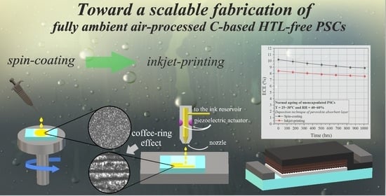
Toward a Scalable Fabrication of Perovskite Solar Cells under Fully Ambient Air Atmosphere: From Spin-Coating to Inkjet-Printing of Perovskite Absorbent Layer

by
Aggeliki Karavioti
1,2,
Dimitris A. Chalkias
1,*,
Giannis Katsagounos
3,
Argyroula Mourtzikou
3,
Alexandros N. Kalarakis
4 and
Elias Stathatos
1,*
1
Nanotechnology & Advanced Materials Laboratory, Department of Electrical and Computer Engineering, University of Peloponnese, GR26334 Patras, Greece
2
Department of Physics, University of Patras, Rio, GR26504 Patras, Greece
3
BRITE Solar Technologies, Patras Science Park, Stadiou Str., Platani, Rio, GR26504 Patras, Greece
4
Department of Mechanical Engineering, University of Peloponnese, GR26334 Patras, Greece
*
Authors to whom correspondence should be addressed.
Submission received: 2 July 2021 / Revised: 30 July 2021 / Accepted: 4 August 2021 / Published: 8 August 2021

Abstract

:
Up until now, the vast majority of perovskite solar cells (PSCs) have relied on the spin-coating of perovskite precursor solution under inert fully controlled conditions, with the performance of solar cells that are developed by alternative techniques and under an ambient atmosphere to lag far behind. This impedes the technology transfer from the laboratory to industrial large-scale production; thus, the investigation of new scalable techniques should be thoroughly considered. The present work constitutes one of the few investigations on the application of inkjet-printing as an advanced alternative technique to the conventional spin-coating technique used for the fabrication of fully ambient air-processed perovskite absorbent layers for carbon-based hole transport layer-free PSCs. A systematic study of the characteristics of the perovskite material and solar cells indicated that the coffee-ring effect combined with poor ink penetration into the mesoporous network of the anode semiconductor were the main reasons for obtaining poor perovskite structure morphology and lower PSC performance by inkjet-printing, which arises from a lower internal quantum efficiency and an increased charge transfer and recombination rate. On the other hand, the crystallinity and optical characteristics of the materials obtained by the compared techniques did not differ considerably, while small differences were observed in the hysteretic behavior and long-term stability of the solar cells.

Graphical Abstract

1. Introduction

Solar photovoltaic (PV) energy accounts for only a small part of global electricity production, although it has the potential to meet the global energy needs by several folds through the use of currently available technologies [1]. High costs and low power conversion efficiency (PCE) have been the major bottlenecks in the development of solar PV power to become a primary source of energy, while engineering the characteristics of PVs is required to open the way for pioneer and niche applications [2,3,4]. To deal with this situation, the development of emerging PV technologies is currently investigated, promising a low levelized cost of electricity (LCOE), additionally offering a plethora of advantages and unique characteristics [5]. Some of them are flexibility, lightweight, transparency and appealing aesthetics. Simultaneously, the lower energy and mass requirements in manufacturing may also lead to a decrease in the overall environmental footprint, which is important for the sustainable development of humanity.
Amongst the emerging PV technologies, hybrid organic–inorganic perovskite solar cells (PSCs) are considered to be a breakthrough technology, providing extraordinary optoelectronic characteristics that lead to a high PCE with simple and low-cost manufacturing. Within a short period, the PCE of PSCs has climbed to 25.5% [6] from the first reported 3.8% in 2009 [7]. The challenge now lies in attaining satisfactory stability and translating these characteristics to commercially feasible scales produced by industrial fabrication methods. To this aim, fully ambient air-processed carbon-based hole transport layer-free (C-based HTL-free) PSCs have attracted significant interest. The commercialization and mass production of C-based HTL-free PSCs is favored due to several reasons, including the low cost of carbon materials, simple design, full compatibility with printing fabrication techniques, all of which are combined with high stability, which is usually much higher compared to that of conventional metal electrode devices. For these reasons, this architecture is considered to be the front runner to the PV market [8]. Today, the record PCE of C-based HTL-free PSCs exceeds 15%, while their outstanding stability has been demonstrated by many research groups [9,10,11]. One noteworthy achievement was attained by Tao et al., who developed a fully ambient air-processed C-based HTL-free PSC that is able to provide 16.25% PCE and retains >90% of its initial performance for 22 weeks [10].
Nevertheless, most of the achievements found so far in the literature are realized with conventional lab-scale spin-coating deposition of the perovskite absorbent layer, with only few studies dealing with alternative scalable deposition techniques that could lead to the commercialization of PSC technology. The spin-coating technique has obvious disadvantages for large-scale and mass production. The primary limitation is that it has low throughput compared to other fabrication techniques since it is inherently a batch process (single substrate) [12]. The actual material usage with spin-coating is also very low (10% or less), as the rest of the material is flung off the side. This is not an issue for lab-scale development but is clearly wasteful for industrial manufacturing. However, the usage of spin-coating for the development of solution-processed perovskite films has seemed ideal up until now. This is because with the precise control of the centrifugal force, the solvent evaporation of the perovskite precursor solution is highly controlled, which has a direct effect on the crystallization kinetics of the material. On the other hand, to develop scalable fabrication processes for solution-processed perovskites, many deposition techniques have been explored, including blade-coating [13], slot-die coating [14], spray-coating [15] and inkjet-printing [16]. Amongst them, inkjet-printing stands out as a digital deposition approach for solution-based materials that is characterized for its scalability, fast material deposition with high accuracy and low waste, which also allows for the formation of fine patterns of printed inks at a high resolution [17].
To date, even though the studies on inkjet-printed PSCs are only few, substantial achievements have been made, both with one-step and two-step perovskite deposition methods [18,19]. Efficiencies higher than 21% have been recently reported for conventional metal electrode (usually Au-based) devices [20]. Regarding the C-based PSCs, the reports are very few but with noteworthy achievements being demonstrated. In 2014, Yang et al. first reported the fabrication (in a homemade glove box) of a planar PSC of an FTO/TiO2/CH3NH3PbI3/C structure using a C+CH3NH3I ink strategy, attaining 11.6% PCE, providing a major step towards the fabrication of low-cost, large-scale, metal electrode-free and efficient PSCs [21]. About three years later, Grätzel et al. attained the development of air-processed infiltrated C-based PSCs, demonstrating efficiencies up to 8.5% and 9.5%, and outstanding stability under harsh UV-light and 1-sun light soaking, respectively [22,23]. However, according to the authors’ knowledge, no reports have been made later in the literature on this promising architecture of PSCs employing an inkjet-printed perovskite absorbent layer. Key issues concerning the inkjet-printing of solution-processed perovskites remain unresolved, especially for ambient air-processing, which typically lead to lower performance and stability in PSCs compared to the devices fabricated by spin-coating.
This work provides a direct comparison between spin-coating and inkjet-printing techniques applied for the fabrication of the perovskite absorbent layer of fully ambient air-processed C-based HTL-free PSCs. In this way, the key challenges that appeared when passing from the conventional lab-based spin-coating to the scalable inkjet-printing manufacturing were demonstrated. The perovskite materials fabricated by the compared deposition techniques were thoroughly characterized regarding their crystal structure, morphology and optical characteristics. The differences in the characteristics regarding the performance, the hysteretic behavior, the quantum efficiency, the charge transport and recombination kinetics, as well as the long-term stability of the solar cells, were also discussed in detail.

2. Materials and Methods

2.1. Materials

Fluorine-doped tin oxide (FTO) glass (TEC 8, 3.2 mm thickness, Pilkington), 1-propanol (assay 99.97%, Lach-ner), titanium(di-isopropoxide) bis(2,4-pentanedionate) 75% in isopropanol (Alfa Aesar), titanium dioxide nano-powder (P25, Degussa), n,n-dimethylformamide (DMF) (ACS for analysis, assay ≥99.9%, Carlo Erba Reagents), methylammonium iodide (MAI) (purity >99%, TCI), lead iodide (PbI2) (ultra-dry ≥99.999%, Alfa Aesar), graphite powder (purity 99%, APS 7-11 micron, Alfa Aesar), carbon black powder (particle size 50 nm, Cabot) and silver paste (Electrodag 1415, Agar Scientific) were used.

2.2. Fabrication of the Solar Cells

C-based HTL-free PSCs were fabricated entirely under uncontrolled ambient atmosphere conditions (40–60% RH) according to the procedure described below. A piece of FTO glass, which was previously cut to the desired dimensions and chemically etched to retain a pattern electrode, was used as a substrate to develop n-i-p PSCs; this was preceded by the thorough cleaning of the substrate using detergent, deionized water and acetone, followed by its calcination at 500 °C to remove any contaminants. On the surface of the FTO glass, an ultra-thin compact titanium dioxide (c-TiO2) layer was fabricated using a solution of titanium(di-isopropoxide) bis(2,4-pentanedionate) 75% in isopropanol diluted (1/9 v/v) in n-propanol by spin-coating it at 2000 rpm and through calcination at 500 °C for 10 min. The procedure was repeated three additional times to obtain the appropriate film thickness. On the top of the c-TiO2 layer, a mesoporous titanium dioxide (m-TiO2) layer was fabricated using a homemade titania nanopaste, which was prepared according to a simple chemical technique described in previous work [24], spin-coated at 3500 rpm, and sintered at 500 °C for 30 min. The perovskite precursor solution was composed of 1 M MAI and 1 M PbI2 in DMF; its preparation was conducted at room temperature conditions, and the solution was filtered through a 0.45 μm PTFE filter before its usage. To fabricate the main active layer of the solar cells, two deposition techniques were tested. The first one was the conventional spin-coating technique: a pre-defined volume of perovskite precursor solution was deposited onto the TiO2-based substrate using an electronic pipette and spun-cast at 1000 rpm for 15 s and at 4000 rpm for 45 s (two steps spin-coating). The second technique was the advanced inkjet-printing: the perovskite precursor solution was printed (double-pass) on the TiO2-based substrate using a Fujifilm Dimatix DMP-2850 inkjet-printer, which was equipped with 16-piezoelectric jetting nozzles of 21 μm diameter, spaced at 254 μm (nozzle spacing). The droplet volume (10 pL), droplet spacing (31 μm), jetting velocity (4.5 m/s) and printing speed (155 mm/s) were held constant, which were fixed according to a preliminary optimization of the printing parameters to obtain an equal thickness of the inkjet-printed perovskite absorbent layer to the corresponding of spin-coated one for comparison purposes. In both deposition techniques, the substrate and the perovskite precursor solution were preheated at 60 °C to avoid any moisture effect, according to previous studies [25,26], and the annealing of the perovskite layer was conducted at 100 °C for 20 min. On the top of the main active layer, a carbon layer was fabricated by doctor-blading a homemade low-temperature carbon paste that presented benign compatibility with the perovskite, which was prepared according to a previous report [27]; its calcination was conducted at 70 °C for 30 h. Finally, a silver paste was used to fabricate the contacts of the solar cells to efficiently collect the photo-current. The active area of the solar cells was equal to the aperture area of a shading mask (0.059 cm2) that covered the rest electrode area, preventing the incidence of light from the edges [28].

2.3. Characterization

X-ray diffraction (XRD) was used to determine the crystal structure of the perovskite absorbent layers from 5° to 60° at a scan rate of 2°/min (Bruker D8 Advance diffractometer equipped with a Cu-Ka monochromatic radiation source (λ = 1.5496 Å) (Bruker, Karlsruhe, Germany)). Optical microscopy and scanning electron microscopy (SEM) were employed to investigate the morphology of the perovskite layers (built-in camera of the inkjet-printer (Fujifilm, NY, USA), Zeiss SUPRA 35 VP microscope (ZEISS, Oberkochen, Germany), respectively). Diffuse reflectance spectroscopy (DRS) was employed to evaluate the absorbance and reflectance spectra of the FTO glass/c-TiO2/m-TiO2/perovskite system, as well as those of the sole perovskite layer, from 300 nm to 800 nm using an interval wavelength of 5 nm (Jasco V-770 spectrophotometer equipped with a 60 mm integrating sphere (JASCO, Easton, PA, USA)). The solar cells were characterized under 1000 W/m2, AM 1.5 G and 25 °C (standard test conditions, STC) using a Solar Light (16S-300) solar simulator (Solar Light, Glenside, PA, USA); the current–voltage (I–V) curves of the solar cells were recorded at a scan rate of 250 mV/s (Keithley 2601 source meter). The incident photon-to-electron conversion efficiency (IPCE) of the solar cells was evaluated using a ThetaMetrisis PM-QE equipped with a Xenon light source using a filter monochromator (Oriel Cornerstone™ 260 1/4 m, Newport (Newport, Irvine, CA, USA)), which was controlled by PM-Monitor® software. The measurements were conducted from 300 nm to 800 nm using an interval wavelength of 5 nm and a time delay of 0.2 s. Electrochemical impedance spectroscopy (EIS) was employed to evaluate the charge transport and recombination kinetics inside the solar cells (Metrohm Autolab 3.v potentiostat galvanostat (Model PGSTAT 128 N) (Metrohm, Utrecht, The Netherlands)). The measurements were recorded at -VOC forward bias over the frequency range from 1 MHz to 1 Hz using ±10 mV perturbation at room temperature in the dark.

3. Results and Discussion

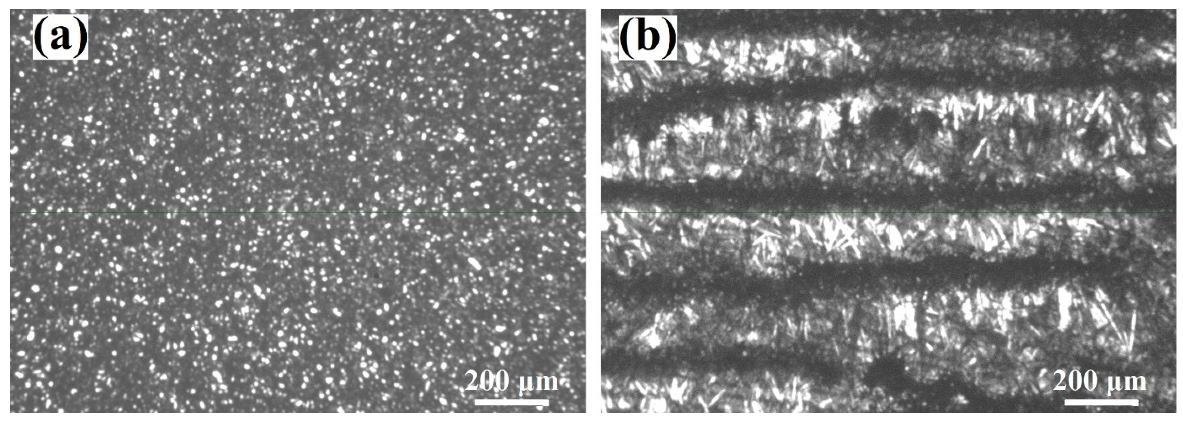
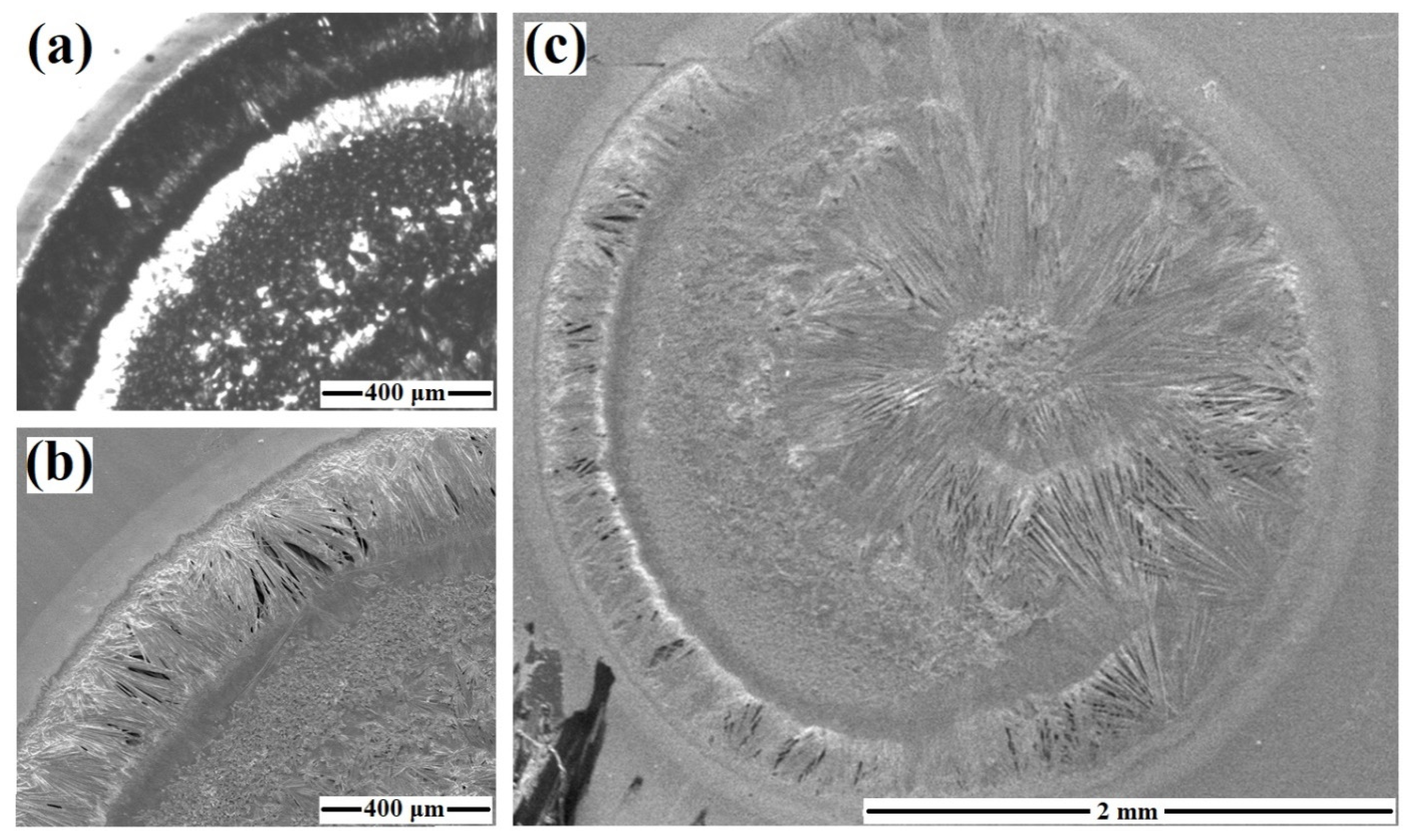
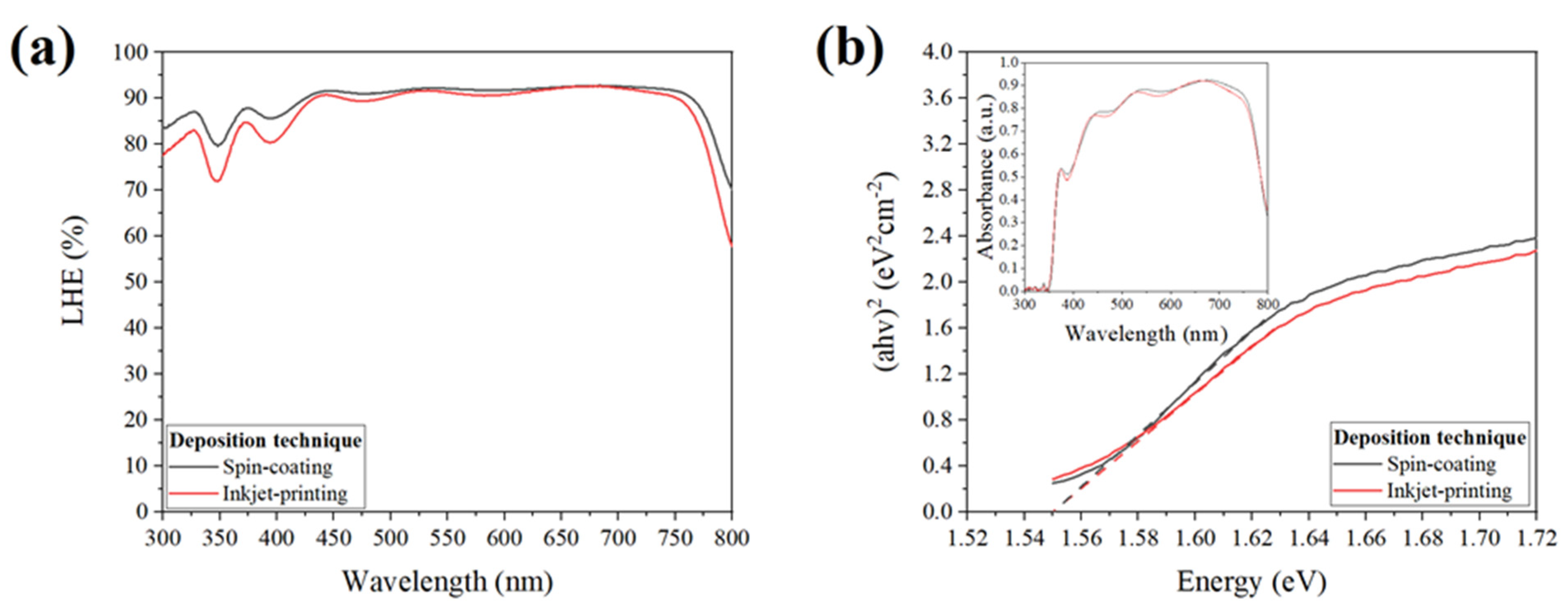
3.1. Characteristics of the Perovskite Absorbent Layer

XRD analysis was conducted to quantify the differences in the crystal structure of the perovskite absorbent layer fabricated using either the conventional spin-coating or the scalable inkjet-printing technique. The XRD patterns of both perovskite layers fabricated on the m-TiO2 are presented in Figure 1. The typical peaks at 14.27°, 20.17°, 23.64°, 24.64°, 28.61°, 31.06°, 32.05°, 35.11°, 40.60°, 42.76°, 43.20°, and 50.33° correspond to the (110), (200), (211), (202), (220), (213), (310), (312), (224), (323), (314), and (404) lattice planes of the tetragonal phase MAPbI3 [29]. The peak detected at 25.38° is attributed to the characteristic anatase (101) lattice plane (JCPDS: No 21-1272), while the peaks at 26.62°, 33.83° 37.86°, 51.60°, and 54.60° are assigned to the (110), (101), (200), (211), and (220) lattice planes of the tetragonal phase SnO2, arising from the FTO glass [30].
As it can be observed, for both cases, a pure MAPbI3 crystal structure is developed, which is free of residues from the precursor materials, with the latter being a common observation when the fabrication of solution-processed perovskite layers takes place under uncontrolled ambient atmosphere conditions [31]. The analysis of the primary (110), (220) and (310) perovskite diffraction peaks by the full width at half maximum (FWHM) using Scherrer’s formula (Equation (1)) [32], where K is taken as 0.9, λ is the wavelength of the X-ray radiation and β is the line width at half-maximum height, showed that the compared materials present almost the same mean crystal sizes in the primary crystal planes, with the largest being observed at the (220) crystal plane, which was found at about 130 nm.
L = K λ / ( β cos θ )
Continuing with the analysis of the surface of the perovskite absorbent layers, several interesting observations regarding the morphology of the compared materials were made. Figure 2 presents top-view optical microscopic images of the perovskite absorbent layer fabricated using the spin-coating and inkjet-printing techniques, demonstrating the morphology of the perovskite films in the case of each deposition technique at a large area.
As it can be observed, the compared films possess quite different surface morphologies. Unlike spin-coating, inkjet-printing led to the development of a discontinuous perovskite film on the m-TiO2 layer, with large areas of the substrate being highly uncovered (bright area) by the perovskite structures (dark area). This could be the result of several interconnected reasons that are mainly related to the composition of the ink, the wetting of the substrate by the ink, as well as the printing parameters [16]. For the present study, a preliminary optimization of the printing parameters took place to achieve an equal thickness of both the perovskite absorbent layer achieved through inkjet-printing and the one produced by spin-coating (see Figure 3a,b), while the materials and fabrication conditions were attempted to be kept the same for comparison purposes.
In the case of inkjet-printing, the development of a high-quality perovskite film is a matter of simultaneous optimization on three main levels. The first one is related to the development of a suitable perovskite precursor ink. For solution-based inks, the precursor materials should be easily convertible into a target film of high purity, minimizing the coffee-ring effect, which results in an inhomogeneous structure and morphology (a discussion on the topic follows in the next paragraph of the paper) [33]. For this reason, the applied perovskite precursor solutions in inkjet-printing should be of a much higher concentration compared to the corresponding ones used for spin-coating, which are usually solvent-rich. This is mainly because in inkjet-printing, the solvent evaporation rate is quite a bit lower than in the case of spin-coating, giving rise to fluid mechanically driven artifacts, leading to a poor crystal structure, which is unlike the case of spin-coating, where most of the solvent can be quickly removed through centrifugation [34]. The second one is related to the wettability of the substrate by the ink. The wetting behavior of the substrate surface by the ink droplets can be classified into three categories: de-wetting, over-wetting and optimal wetting [20]. De-wetting describes a contraction of the as-printed droplets on the surface without the formation of a continuous wet film. Over-wetting describes an inhomogeneous spread of droplets across the substrate, with the worst case being no pinning behavior. Optimal wetting behavior is achieved by a minimum contact angle of 5°–10° between the substrate surface and the droplet, which is needed to avoid over-wetting. The theoretical upper limit of the contact angle is θ < 90° since, in this case, the droplets start to repel from the surface, leading to de-wetting. To achieve an optimal contact angle, the surface tension of the ink and the surface free energy of the substrate need to be adjusted. This is dependent on the temperature of the perovskite ink and the substrate. In the present case, the temperature of the aforementioned materials was fixed at about 60 °C, according to previous studies conducted in the area of temperature optimization for the substrate and perovskite precursor solution to develop corresponding systems entirely under ambient atmosphere [25,26]. The contact angle measurements for the same materials and fabrication conditions have shown a value of about 12° in previous studies [26]. The third level of optimization is related to the printing parameters, e.g., droplet volume and spacing, jetting velocity, and printing speed, where, in turn, their optimization is dependent on the formulation of the perovskite ink and the wetting of the substrate by the ink. Therefore, it is understood that the optimization of the whole printing process requires systematic and holistic engineering since the modification of one of the factors can influence all other parameters [16].
To give further evidence of the differences in the morphology of the perovskite absorbent layer fabricated by the two compared techniques, SEM analysis followed. As it can be observed from Figure 3c,d, and clearer viewed in the higher magnification SEM images presented in the inset of the corresponding figures, the morphology of the MAPbI3 films is based on rod-shaped structures in both cases, which leads to incomplete coverage of the TiO2 film underneath. This observation is common for ambient air-processed MAPbI3, and it is one of the main reasons for attaining low performance in PSCs fabricated under uncontrolled ambient atmosphere compared to the corresponding devices fabricated under inert and fully-controlled conditions [35]. Generally, this morphology results in reduced light absorption by the perovskite absorbent layer and minimizes the photo-current production. At the same time, the exposed surface of the electron transport layer (the m-TiO2 for the present case) can come into direct contact with the hole transport layer (the carbon electrode for the present case), thereby resulting in a low shunt resistance, a high charge recombination rate, and subsequently in reduced photo-voltage production. By pointing out the differences in the morphology of the perovskite films fabricated by spin-coating or inkjet-printing, several noteworthy observations can be extracted. More specifically, in the former case, the perovskite rod-shaped structures grew uniformly on the entire area of the m-TiO2 substrate, as is usually observed. On contrary, under the same conditions, a discontinuous perovskite film morphology is developed via inkjet-printing, with the density of the rod-shaped structures varying from one area to another, which is in agreement with the observations obtained from the optical microscopic images presented before. This is attributed to the coffee-ring effect, which leads to inhomogeneous crystallization phenomena (see Figure 4).
According to classic nucleation theory, a solution must be in a supersaturated state to initiate crystallization; namely, it must reach the critical supersaturation concentration (Ccs). For the present case (solution-processed perovskites), with the continuous evaporation of the solvent of the perovskite precursor solution, the solution exceeds the Ccs, and consequently, small nuclei are generated. Subsequently, additional solutes tend to precipitate, either creating new nuclei or promoting the growth of the formerly generated nuclei. Thus, there is competition between nuclei formation and growth in consuming the solute. This is governed by the quench depth (ΔC); namely, the difference between the highest concentration and the super-saturation concentration. If the depth is high, nuclei formation dominates the crystallization process, while, in the case of a low depth, nuclei growth dominates the crystallization process instead [36]. As it is perceived, solvent evaporation is a dominant factor in this process. For the case of inkjet-printing, the evaporation rate of the solvent on the droplet surface is not uniform; namely, the edge region dries faster than the center region, and thus, the edge region starts nucleating first. At the same time, there is an outward convective flow that leads to an edge-enriched material agglomeration, a phenomenon that is known as the coffee-ring effect [33,37]. For the present case, the sparse and dense perovskite structure regions are considered regions where the solvent evaporation rate is low and high, respectively (the inkjet-printhead possibly spreads the material in the former area, with the material finally migrating to the latter area). These observations can be correlated to the corresponding morphologies observed for high and low humidity-processed MAPbI3, where the solvent evaporation is low and high, and the rod-shaped structures are sparse and dense, respectively [36]. Noteworthy are also the observations that can be determined by the higher magnification SEM images presented in the inset of Figure 3c,d (taken in the high-density perovskite structure area). As evidenced from the images, the rod-shaped structures are denser and without deterioration in the case of inkjet-printing compared to spin-coating. This could be attributed to a reduced humidity effect on the perovskite material, which would have arisen from the precise control of the temperature of the substrate and the perovskite ink during the entire duration of the inkjet-printing process, unlike in the spin-coating case, where this was not possible. Humidity greatly affects the crystal and chemical structure and the morphology of hybrid organic—inorganic perovskites [35]. Regarding the morphology, this is evidenced by phenomena such as the deterioration of the perovskite structure (e.g., crystal grain, boundary creep), as well as an enlargement of the percentage of the uncovered area of the substrate by the perovskite structures.
To shed light on the differences in the absorbance characteristics of the perovskite films fabricated by spin-coating and inkjet-printing techniques, DRS measurements were conducted in the spectral range of 300 to 800 nm. Figure 5a presents the light-harvesting efficiency (LHE) of the perovskite films fabricated on the m-TiO2 layer, calculated using Equation (2), where A and R represent the absorbance and reflectance spectra of the sample, respectively [38]. The optical bandgap of the compared materials (sole perovskite layer) was obtained from the Tauc plots shown in Figure 5b, assuming a direct transition.
L H E = ( 1 R ) ( 1 10 A )
As shown in Figure 5a, both samples presented a high LHE, which was found to be almost identical for the spectral region of 450 to 750 nm, at about 90%. The lower LHE measured for the spectral regions of 300 to 450 nm and 750 to 800 nm for the inkjet-printed sample compared to the spin-coated one could be attributed to the incomplete penetration of the perovskite ink into the m-TiO2 network, a situation that enhances the light scattering by the wide-bandgap semiconductor. This is possibly due to the inherently very low material usage by inkjet-printing compared to spin-coating, and also arising from the non-optimal ink formulation and printing parameters. On the other hand, in both cases, the optical bandgap of the samples was found at 1.55 eV, which is in agreement with the reported values in the literature [39].

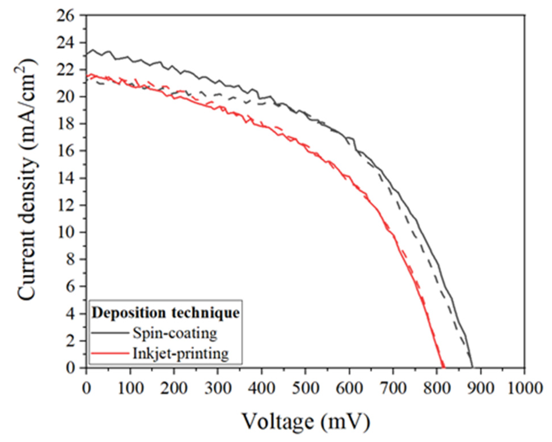
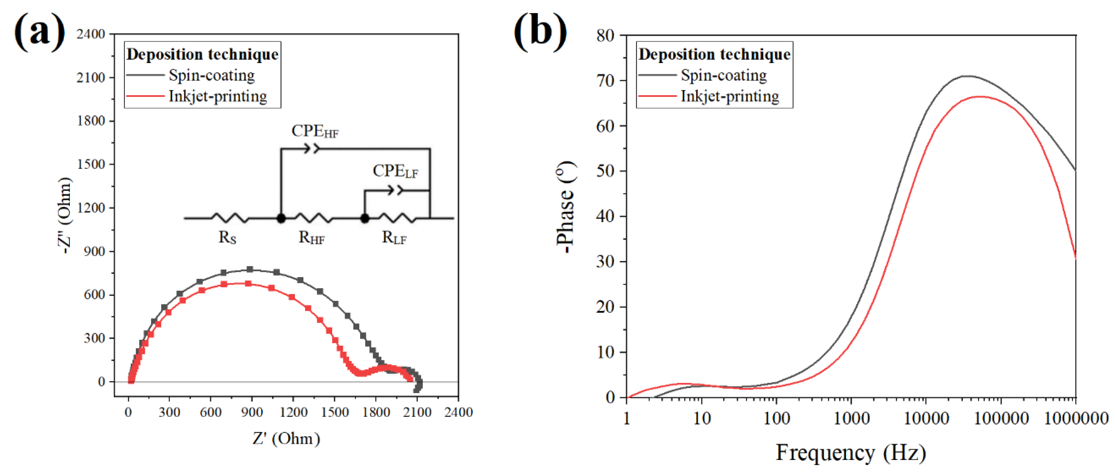
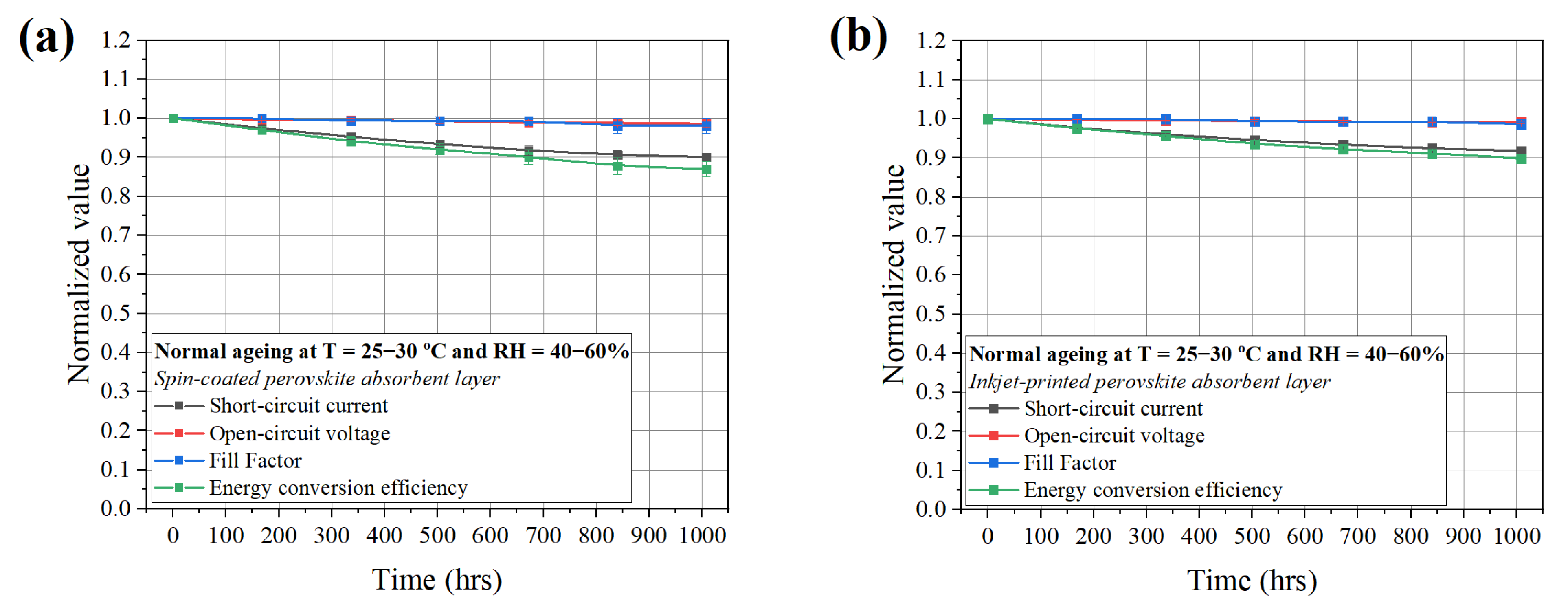
3.2. Characteristics of the Solar Cells

Figure 6 presents representative J–V characteristic curves (forward and reverse scan) of small-sized PSCs fabricated by the spin-coating or inkjet-printing of the perovskite absorbent layer, while their electrical characteristics are tabulated in Table 1.
By comparing the electrical characteristics of the solar cells, it is demonstrated that the devices fabricated by the inkjet-printing technique can achieve quite a satisfactory performance compared to the corresponding solar cells fabricated by spin-coating, even though the printing process was not optimized. In the former case, the PCE of the solar cells was found at about 8.40%, slightly reduced compared to the performance of the latter devices, whose PCE was found at about 10%. The lower performance attained by the solar cells employing the inkjet-printed perovskite absorbent layer compared to the devices employing the spin-coated one was mainly attributed to the decreased values of VOC and FF, while slightly reduced values were also found for JSC.
The hysteretic phenomena in the electrical characteristics of both types of devices were also investigated since they are a critical issue related to the performance and stability of PSCs. The hysteresis index (HI) was calculated using Equation (3).
H I = S C O C J r e v ( V ) J f o r ( V ) d V S C O C J r e v ( V ) d V
As it is observed, in both cases, the solar cells demonstrated a low HI, with the absolute values ranging lower than 10%. By comparing the hysteretic characteristics of the two different devices, it is evidenced that the PSCs employing the inkjet-printed perovskite absorbent layer present an almost absent normal hysteresis, while the devices employing the spin-coated perovskite absorbent layer show a slightly more intense and inverted hysteresis. According to the literature, the normal hysteresis presented in PSCs is attributed to the existence of a capacitive current before reaching the steady-state current, namely, there is an accumulation of charges in the forward scan (“capacitor filling”) and a release of charges in the reverse scan (“capacitor emptying”) [40]. On the other hand, the inverted hysteresis is intimately related to phenomena of negative capacitance, which are associated with surface interactions with vacancies/ions at the electron transport layer/perovskite interface [41]. A more and in-depth discussion on the origins of the obtained PV parameters variation is given in the following paragraphs through the quantum efficiency and impedance measurements on PSCs.
Figure 7 presents the measurements of external and internal quantum efficiency of the solar cells employing the spin-coated or inkjet-printed perovskite absorbent layer. Compared to the spin-coated device (integrated JSC 22.23 mA/cm2), the inkjet-printed device (integrated JSC 20.92 mA/cm2) showed slightly lower IPCE values in the spectrum region of 350 to 750 nm, which is in agreement with the results coming from the J–V characterization of the solar cells. To better understand the origin of this difference, absorbed photon-to-current conversion efficiency (APCE) spectra were calculated using Equation (4), providing information on the nature of the charge injection efficiency of the solar cells [38].
A P C E = I P C E L H E
The APCE spectra demonstrated that the difference in the collected photo-current is mainly attributed to the better charge collection efficiency of the carriers generated from almost the entire visible light spectrum (400 to 750 nm) by the spin-coated perovskite absorbent layer compared to the inkjet-printed one. On the other hand, the corresponding difference in the shorter wavelengths arises from the better LHE. The aforementioned observations could be attributed to the poor penetration of the perovskite ink into the mesoporous network of the TiO2, the thickness of which is possibly high for inkjet-printed PSCs, increasing the light scattering by the wide-bandgap semiconductor (short wavelengths region) and reducing the collection efficiency of low-energy electrons (long wavelengths region). Something noteworthy is that the value of the APCE spectra of both devices for wavelengths of about 400 nm almost reached 100%. This observation agrees with the reported ones in the literature, with PSCs employing MAPbI3 structures attaining almost 100% internal quantum efficiency in single junction configuration, highlighting that further improvements in the performance of these cells would be particularly difficult by further optimizing the single absorber layers [42].
Continuing the characterization of the solar cells to give further evidence in the differences in the characteristics of the compared devices, impedance spectroscopy was used as an effective tool to evaluate the charge transfer and recombination processes taking place in each type of PSC. Figure 8 shows the Nyquist plots and the Bode phase diagrams of the PSCs fabricated by the spin-coated or inkjet-printed perovskite absorbent layer, while the parameters extracted from the EIS analysis are tabulated in Table 2.
As it is observed, the Nyquist plots of both types of devices are characterized by the presence of two semicircles: one big arc at the high-frequency domain and a much smaller arch at the low-frequency domain. The first one is related to bulk recombination and geometric capacitance, while the latter is related to an accumulation of both electronic and ionic charges at the interfaces of the perovskite layer with the charge selective contacts [43]. The negative capacitance feature that appeared at the low-frequency domain is a common observation in the EIS spectra of PSCs but with no clear physical origin. This phenomenon is hypothesized to appear due to delayed dynamics caused by either an accumulation of charges at the interfaces or by ionic redistribution controlling charge injection [43]. The inverted hysteresis and the negative capacitance in the low-frequency domain are also reported familiar features, something that was also observed in the present study (the PSCs with the spin-coated perovskite absorbent layer presented inverted hysteresis and negative capacitance features) [41].
Considering that the performance of solar cells under operation can be deduced solely from the impedance response at the high-frequency domain, a simplified equivalent circuit (see inset of Figure 8a) was applied to fit the experimental results above the Z’ axis [44]. In this way, the series resistance (Rs) and the high-frequency resistance (RHF) are extracted with high accuracy, providing information on the charge transport and recombination (RrecRHF) taking place inside both types of devices. By comparing the impedance spectra of the PSCs employing the spin-coated and inkjet-printed perovskite absorbent layer, it is observed that the former type of devices presents a lower Rs and a higher RHF compared to the latter devices. This implies a better charge transport and a decreased charge recombination rate inside the solar cells. The aforementioned observations can be attributed to two main reasons that limit the performance of PSCs fabricated by the inkjet-printing of the perovskite absorbent layer. The first one is attributed to the poor penetration of the perovskite ink inside the mesoporous network of TiO2 during the inkjet-printing process, as discussed in the DRS and IPCE analysis. The second one is in regard to the poor morphology of the inkjet-printed perovskite absorbent layer, which leads to a discontinuous morphology, with a large surface of the electron transport layer being exposed, which can come in direct contact with the hole transport layer, resulting in a low shunt resistance and a high charge recombination rate, as discussed in the SEM analysis. The increased recombination rate inside the solar cells fabricated by the inkjet-printing of the perovskite absorbent layer compared to the spin-coated one is also evidenced by the decreased values of the average electron lifetime (τe), which were calculated from the frequency value of the peak in the high-frequency domain of the Bode phase diagrams.
The results are in agreement with the corresponding ones coming from the J–V and APCE characterization of the solar cells, with the PSCs fabricated by inkjet-printing of the perovskite absorbent layer demonstrating lower PV performance compared to the corresponding devices employing the spin-coating perovskite absorbent layer, although the former ones have great prospects for further optimization, as well as provide the potential to scale-up the technology.
Stability studies on solar cells by means of their dark storage at room temperature conditions provide important information on the tolerance of these devices to moisture, oxygen, and other aggressive atmospheric components that are naturally presented in the air (e.g., CO2, NOx) [45]. In the present investigation, the stability of the PSCs fabricated by the spin-coated or inkjet-printed perovskite absorbent layer was evaluated by storing the solar cells in the dark under the environmental conditions of T = 20–25 °C and RH = 40–60%, and measuring their J–V characteristics for a total duration of an experiment of about 1000 h with time intervals of 168 h (every week).
As it is observed in Figure 9, both of the unencapsulated solar cell devices presented noteworthy stability, retaining higher than 85% of their initial performance after 1000 h of ageing. In both cases, the main reason for the degradation of their PCE was the decrease in the JSC, while VOC and FF did not show any notable variation. Similar results were found in the literature [46]. The decrease in JSC with time was mainly attributed to the degradation of the perovskite absorbent layer. According to previous studies, H2O can form a complex with CH3NH3PbI3, forming a hydrate product, similar to (CH3NH3)4PbI6·2H2O. This causes a decrease in the absorbance spectrum of the material across the visible region of the light spectrum, subsequently reducing the external quantum efficiency of the solar cell [46]. By comparing the two different types of devices, it is evidenced that the PSCs employing the inkjet-printed perovskite absorbent layer present slightly better stability in time compared to the corresponding devices fabricated by the spin-coating of the perovskite absorbent layer. This can be attributed to a lower humidity effect on the solar cells during the fabrication stage since with inkjet-printing, precise control of the temperature of the substrate and the perovskite ink was possible during the entire inkjet-printing process, unlike in the spin-coating case, which was quite difficult.

4. Conclusions

This work provides a direct comparison between spin-coating and inkjet-printing techniques for the fabrication of fully ambient air-processed perovskite absorbent layers for C-based HTL-free PSCs. The materials formulation, the solar cells design, and the preparation/fabrication conditions were attempted to be kept the same for both cases for comparison purposes to unveil the key differences in the characteristics of the materials and the corresponding solar cells developed by each type of technique. The results showed that the main differences arise for the morphology of the perovskite film, which had a subsequent impact on the characteristics of the solar cells, while the crystal structure and optical characteristics of the perovskite absorbent layers did not differ considerably.
More specifically, the inkjet-printed perovskite layer presented a discontinued morphology, with large areas of the underneath electron transport layer being uncovered by the perovskite rod-shaped structures, unlike in the case of spin-coating, where a uniform morphology was obtained. This was attributed to the coffee-ring effect, which is intense during the inkjet-printing of solvent-rich perovskite precursor inks, such as the one used in the present case. Moreover, the corresponding FTO/c-TiO2/m-TiO2/perovskite system fabricated by inkjet-printing presented a lower LHE, mainly at the regions of 300–400 nm and 750–800, compared to the one fabricated by spin-coating. The aforementioned observation was assigned to the poor penetration of the perovskite precursor ink into the mesoporous network of TiO2, a situation that enhances the light scattering by the wide-bandgap semiconductor. This is possibly due to the inherently very low material usage during inkjet-printing compared to spin-coating, also arising from the non-optimal ink formulation and printing parameters. On the other hand, the crystallinity of the compared perovskite materials did not differ since in both cases, an equal mean crystallite size in all three primary MAPbI3 crystal planes was obtained, while residues of the perovskite precursor materials were not observed for any of the samples.
Regarding the solar cells, the characteristics of the compared devices did not differ considerably, with the PCE of the PSCs employing the inkjet-printed perovskite absorbent layer to be 16% lower compared to the corresponding one of PSCs employing the spin-coated material. This was mainly due to the decreased VOC and FF, while the JSC value was also found slightly reduced. Something noteworthy is that both types of devices presented mild hysteretic behavior ( | H I | < 10%), with the absolute value of HI being lower in the case of inkjet-printing. The measurements of the external and internal quantum efficiency of the solar cells showed that the collection efficiency of the photo-generated charges was better for the case of spin-coating, while these devices were also characterized by a lower charge transfer resistance and recombination rate. This was attributed to the poor penetration of the perovskite precursor ink into the mesoporous network of TiO2, as well as to the discontinuous morphology of the perovskite absorbent layer, which can lead to direct contact of the electron transport layer (herein the TiO2) and the hole transport layer (herein the carbon electrode), and the subsequent reduction of shunt resistance, in the case of inkjet-printing. Finally, noteworthy stability under T = 20–25 °C and RH = 40–60% was obtained for both types of devices employing the spin-coated and inkjet-printed perovskite absorbent layer. Both types of solar cells were able to retain higher than 85% of their initial performance after 1000 h of ageing without the use of a sealant (almost 90% for the case of inkjet-printing). The degradation of the performance of the solar cells over time was attributed to the decrease in JSC, possibly due to the degradation of the perovskite absorbent layer, where moisture from the ambient air can complex with CH3NH3PbI3, forming hydrate products. The results discussed herein can provide important information that can help advance PSCs toward their commercialization in the near future.

Author Contributions

The authors confirm their contributions to the work conducted in the field of: A.K., methodology, data curation; D.A.C., conceptualization, investigation, methodology, formal analysis, validation, writing—original draft preparation, supervision; G.K., methodology, data curation; A.M., methodology, data curation; A.N.K., data curation; E.S.: visualization, investigation, validation, writing—review and editing, supervision, resources, funding acquisition. All authors have read and agreed to the published version of the manuscript.

Funding

This research has been co-financed by the European Union and Greek national funds through the Operational Program Competitiveness, Entrepreneurship and Innovation, under the call RESEARCH-CREATE-INNOVATE (project code: T1EDK-01082).

Attributions

The graphical abstract was designed using resources from www.freepik.com and www.sketchfab.com. The background was taken from www.freepik.com: Abstract vector created by macrovector—www.freepik.com (https://www.freepik.com/free-photos-vectors/abstract, accessed on 1 July 2021). Pipette 3D model was taken from www.sketchfab.com: “Pipette model” (https://skfb.ly/DvWA, accessed on 1 July 2021) by tompat2552 and is licensed under a Creative Commons Attribution (http://creativecommons.org/licenses/by/4.0/, accessed on 1 July 2021).

Conflicts of Interest

The authors declare no conflict of interest. The funders had no role in the design of the study; in the collection, analyses, or interpretation of data; in the writing of the manuscript, or in the decision to publish the results.

References

  1. Kabir, E.; Kumar, P.; Kumar, S.; Adelodun, A.A.; Kim, K.-H. Solar energy: Potential and future prospects. Renew. Sustain. Energy Rev. 2018, 82, 894–900. [Google Scholar] [CrossRef]
  2. Zhang, N.; Jiang, T.; Guo, C.; Qiao, L.; Ji, Q.; Yin, L.; Yu, L.; Murto, P.; Xu, X. High-performance semitransparent polymer solar cells floating on water: Rational analysis of power generation, water evaporation and algal growth. Nano Energy 2020, 77, 105111. [Google Scholar] [CrossRef]
  3. Deng, H.; Sun, Q.; Yang, Z.; Li, W.; Yan, Q.; Zhang, C.; Zheng, Q.; Wang, X.; Lai, Y.; Cheng, S. Novel symmetrical bifacial flexible CZTSSe thin film solar cells for indoor photovoltaic applications. Nat. Commun. 2021, 12, 3107. [Google Scholar] [CrossRef] [PubMed]
  4. Chalkias, D.A.; Charalampopoulos, C.; Andreopoulou, A.K.; Karavioti, A.; Stathatos, E. Spectral engineering of semi-transparent dye-sensitized solar cells using new triphenylamine-based dyes and an iodine-free electrolyte for greenhouse-oriented applications. J. Power Sources 2021, 496, 229842. [Google Scholar] [CrossRef]
  5. Jean, J.; Brown, P.R.; Jaffe, R.L.; Buonassisi, T.; Bulović, V. Pathways for solar photovoltaics. Energy Environ. Sci. 2015, 8, 1200–1219. [Google Scholar] [CrossRef]
  6. National Renewable Energy Laboratory: Photovoltaic Research. Available online: https://www.nrel.gov/pv/ (accessed on 28 January 2021).
  7. Kojima, A.; Teshima, K.; Shirai, Y.; Miyasaka, T. Organometal halide perovskites as visible-light sensitizers for photovoltaic cells. J. Am. Chem. Soc. 2009, 131, 6050–6051. [Google Scholar] [CrossRef] [PubMed]
  8. Chen, H.; Yang, S. Carbon-based perovskite solar cells without hole transport materials: The front runner to the market? Adv. Mater. 2017, 29, 1603994. [Google Scholar] [CrossRef]
  9. Mohammed, M.K.A. High-performance hole conductor-free perovskite solar cell using a carbon nanotube counter electrode. RSC Adv. 2020, 10, 35831–35839. [Google Scholar] [CrossRef]
  10. Zhou, J.; Wu, J.; Li, N.; Li, X.; Zheng, Y.-Z.; Tao, X. Efficient all-air processed mixed cation carbon-based perovskite solar cells with ultra-high stability. J. Mater. Chem. A 2019, 7, 17594–17603. [Google Scholar] [CrossRef]
  11. Yang, Y.; Liu, Z.; Ng, W.K.; Zhang, L.; Zhang, H.; Meng, X.; Bai, Y.; Xiao, S.; Zhang, T.; Hu, C.; et al. An ultrathin ferroelectric perovskite oxide layer for high-performance hole transport material free carbon based halide perovskite solar cells. Adv. Funct. Mater. 2019, 29, 1806506. [Google Scholar] [CrossRef] [Green Version]
  12. Tufail Chaudhary, K. Thin film deposition: Solution based approach. In Thin Films [Working Title]; IntechOpen: London, UK, 2021. [Google Scholar]
  13. Yang, Z.; Chueh, C.-C.; Zuo, F.; Kim, J.H.; Liang, P.-W.; Jen, A.K.-Y. High-performance fully printable perovskite solar cells via blade-coating technique under the ambient condition. Adv. Energy Mater. 2015, 5, 1500328. [Google Scholar] [CrossRef]
  14. Hwang, K.; Jung, Y.-S.; Heo, Y.-J.; Scholes, F.H.; Watkins, S.E.; Subbiah, J.; Jones, D.J.; Kim, D.-Y.; Vak, D. Toward large scale roll-to-roll production of fully printed perovskite solar cells. Adv. Mater. 2015, 27, 1241–1247. [Google Scholar] [CrossRef]
  15. Barrows, A.T.; Pearson, A.J.; Kwak, C.K.; Dunbar, A.D.F.; Buckley, A.R.; Lidzey, D.G. Efficient planar heterojunction mixed-halide perovskite solar cells deposited via spray-deposition. Energy Environ. Sci. 2014, 7, 2944–2950. [Google Scholar] [CrossRef]
  16. Zhang, L.; Chen, S.; Wang, X.; Wang, D.; Li, Y.; Ai, Q.; Sun, X.; Chen, J.; Li, Y.; Jiang, X.; et al. Ambient inkjet-printed high-efficiency perovskite solar cells: Manipulating the spreading and crystallization behaviors of picoliter perovskite droplets. Sol. RRL 2021, 5, 2100106. [Google Scholar] [CrossRef]
  17. Peng, X.; Yuan, J.; Shen, S.; Gao, M.; Chesman, A.S.R.; Yin, H.; Cheng, J.; Zhang, Q.; Angmo, D. Perovskite and organic solar cells fabricated by inkjet printing: Progress and prospects. Adv. Funct. Mater. 2017, 27, 1703704. [Google Scholar] [CrossRef]
  18. Li, S.G.; Jiang, K.J.; Su, M.J.; Cui, X.P.; Huang, J.H.; Zhang, Q.Q.; Zhou, X.Q.; Yang, L.M.; Song, Y.L. Inkjet printing of CH3NH3PbI3 on a mesoscopic TiO2 film for highly efficient perovskite solar cells. J. Mater. Chem. A 2015, 3, 9092–9097. [Google Scholar] [CrossRef]
  19. Li, P.; Liang, C.; Bao, B.; Li, Y.; Hu, X.; Wang, Y.; Zhang, Y.; Li, F.; Shao, G.; Song, Y. Inkjet manipulated homogeneous large size perovskite grains for efficient and large-area perovskite solar cells. Nano Energy 2018, 46, 203–211. [Google Scholar] [CrossRef]
  20. Eggers, H.; Schackmar, F.; Abzieher, T.; Sun, Q.; Lemmer, U.; Vaynzof, Y.; Richards, B.S.; Hernandez-Sosa, G.; Paetzold, U.W. Inkjet-printed micrometer-thick perovskite solar cells with large columnar grains. Adv. Energy Mater. 2020, 10, 1903184. [Google Scholar] [CrossRef] [Green Version]
  21. Wei, Z.; Chen, H.; Yan, K.; Yang, S. Inkjet printing and instant chemical transformation of a CH3NH3PbI3/nanocarbon electrode and interface for planar perovskite solar cells. Angew. Chem. Int. Ed. 2014, 53, 13239–13243. [Google Scholar] [CrossRef]
  22. Hashmi, S.G.; Tiihonen, A.; Martineau, D.; Ozkan, M.; Vivo, P.; Kaunisto, K.; Ulla, V.; Zakeeruddin, S.M.; Grätzel, M. Long term stability of air processed inkjet infiltrated carbon-based printed perovskite solar cells under intense ultra-violet light soaking. J. Mater. Chem. A 2017, 5, 4797–4802. [Google Scholar] [CrossRef] [Green Version]
  23. Hashmi, S.G.; Martineau, D.; Li, X.; Ozkan, M.; Tiihonen, A.; Dar, M.I.; Sarikka, T.; Zakeeruddin, S.M.; Paltakari, J.; Lund, P.D.; et al. Air processed inkjet infiltrated carbon based printed perovskite solar cells with high stability and reproducibility. Adv. Mater. Technol. 2017, 2, 1600183. [Google Scholar] [CrossRef]
  24. Chalkias, D.A.; Laios, A.I.; Petala, A.; Papanicolaou, G.C. Evaluation of the limiting factors affecting large-sized, flexible, platinum-free dye-sensitized solar cells performance: A combined experimental and equivalent circuit analysis. J. Mater. Sci. Mater. Electron. 2018, 29, 9621–9634. [Google Scholar] [CrossRef]
  25. Lv, Y.; Jin, Y.; Cai, W.; Zhang, Z.; Zhou, X.; Chen, H. Air-processed carbon-based perovskite solar cells with enhanced efficiency and stability: Effect of temperature control and using CuSCN. J. Alloys Compd. 2020, 821, 153272. [Google Scholar] [CrossRef]
  26. Chalkias, D.A.; Karavioti, A.; Kalarakis, A.N.; Stathatos, E. Unveiling the importance of dripping temperature control of hybrid organic-inorganic perovskite precursor solution for the fabrication of fully ambient air-processed perovskite solar cells. Sol. Energy 2021, 224, 1017–1027. [Google Scholar] [CrossRef]
  27. Wang, S.; Jiang, P.; Shen, W.; Mei, A.; Xiong, S.; Jiang, X.; Rong, Y.; Tang, Y.; Hu, Y.; Han, H. A low-temperature carbon electrode with good perovskite compatibility and high flexibility in carbon based perovskite solar cells. Chem. Commun. 2019, 55, 2765–2768. [Google Scholar] [CrossRef]
  28. Wang, Y.; Liu, X.; Zhou, Z.; Ru, P.; Chen, H.; Yang, X.; Han, L. Reliable measurement of perovskite solar cells. Adv. Mater. 2019, 31, 1803231. [Google Scholar] [CrossRef] [PubMed]
  29. Oku, T. Crystal structures of CH3NH3PbI3 and related perovskite compounds used for solar cells. In Solar Cells-New Approaches and Reviews; Kosyachenko, L.A., Ed.; InTech: London, UK, 2015. [Google Scholar]
  30. Asl, H.Z.; Rozati, S.M. High-quality spray-deposited fluorine-doped tin oxide: Effect of film thickness on structural, morphological, electrical, and optical properties. Appl. Phys. A Mater. Sci. Process. 2019, 125, 689. [Google Scholar] [CrossRef]
  31. Zhang, Y.; Kirs, A.; Ambroz, F.; Lin, C.; Bati, A.S.R.; Parkin, I.P.; Shapter, J.G.; Batmunkh, M.; Macdonald, T.J. Ambient fabrication of organic–inorganic hybrid perovskite solar cells. Small Methods 2021, 5, 2000744. [Google Scholar] [CrossRef]
  32. Cullity, B.D. Elements of X-ray Diffraction, 2nd ed.; Addison-Wesley: Boston, MA, USA, 1978. [Google Scholar]
  33. Deegan, R.D.; Bakajin, O.; Dupont, T.F.; Huber, G.; Nagel, S.R.; Witten, T.A. Contact line deposits in an evaporating drop. Phys. Rev. E Stat. Phys. Plasmas Fluids Relat. Interdiscip. Top. 2000, 62, 756–765. [Google Scholar] [CrossRef] [Green Version]
  34. Liang, C.; Li, P.; Gu, H.; Zhang, Y.; Li, F.; Song, Y.; Shao, G.; Mathews, N.; Xing, G. One-Step inkjet printed perovskite in air for efficient light harvesting. Sol. RRL 2018, 2, 1700217. [Google Scholar] [CrossRef]
  35. Mohamad Noh, M.F.; Arzaee, N.A.; Nawas Mumthas, I.N.; Mohamed, N.A.; Mohd Nasir, S.N.F.; Safaei, J.; Yusoff, A.R.B.M.; Nazeeruddin, M.K.; Mat Teridi, M.A. High-humidity processed perovskite solar cells. J. Mater. Chem. A 2020, 8, 10481–10518. [Google Scholar] [CrossRef]
  36. Wang, F.; Zhang, T.; Wang, Y.; Liu, D.; Zhang, P.; Chen, H.; Ji, L.; Chen, L.; Chen, Z.D.; Wu, J.; et al. Steering the crystallization of perovskites for high-performance solar cells in ambient air. J. Mater. Chem. A 2019, 7, 12166–12175. [Google Scholar] [CrossRef]
  37. Schackmar, F.; Eggers, H.; Frericks, M.; Richards, B.S.; Lemmer, U.; Hernandez-Sosa, G.; Paetzold, U.W. Perovskite solar cells with all-inkjet-printed absorber and charge transport layers. Adv. Mater. Technol. 2021, 6, 2000271. [Google Scholar] [CrossRef]
  38. Sheikh, A.D.; Bera, A.; Haque, M.A.; Rakhi, R.B.; Del Gobbo, S.; Alshareef, H.N.; Wu, T. Atmospheric effects on the photovoltaic performance of hybrid perovskite solar cells. Sol. Energy Mater. Sol. Cells 2015, 137, 6–14. [Google Scholar] [CrossRef]
  39. Leguy, A.M.A.; Azarhoosh, P.; Alonso, M.I.; Campoy-Quiles, M.; Weber, O.J.; Yao, J.; Bryant, D.; Weller, M.T.; Nelson, J.; Walsh, A.; et al. Experimental and theoretical optical properties of methylammonium lead halide perovskites. Nanoscale 2016, 8, 6317–6327. [Google Scholar] [CrossRef] [Green Version]
  40. Kang, D.; Park, N. On the current–voltage hysteresis in perovskite solar cells: Dependence on perovskite composition and methods to remove hysteresis. Adv. Mater. 2019, 31, 1805214. [Google Scholar] [CrossRef] [PubMed]
  41. Alvarez, A.O.; Arcas, R.; Aranda, C.A.; Bethencourt, L.; Mas-Marzá, E.; Saliba, M.; Fabregat-Santiago, F. Negative capacitance and inverted hysteresis: Matching features in perovskite solar cells. J. Phys. Chem. Lett. 2020, 11, 8417–8423. [Google Scholar] [CrossRef]
  42. Huang, J.; Xiang, S.; Yu, J.; Li, C.Z. Highly efficient prismatic perovskite solar cells. Energy Environ. Sci. 2019, 12, 929–937. [Google Scholar] [CrossRef]
  43. Bou, A.; Pockett, A.; Raptis, D.; Watson, T.; Carnie, M.J.; Bisquert, J. Beyond impedance spectroscopy of perovskite solar cells: Insights from the spectral correlation of the electrooptical frequency techniques. J. Phys. Chem. Lett. 2020, 11, 8654–8659. [Google Scholar] [CrossRef]
  44. Riquelme, A.; Bennett, L.J.; Courtier, N.E.; Wolf, M.J.; Contreras-Bernal, L.; Walker, A.B.; Richardson, G.; Anta, J.A. Identification of recombination losses and charge collection efficiency in a perovskite solar cell by comparing impedance response to a drift-diffusion model. Nanoscale 2020, 12, 17385–17398. [Google Scholar] [CrossRef]
  45. Khenkin, M.V.; Katz, E.A.; Abate, A.; Bardizza, G.; Berry, J.J.; Brabec, C.; Brunetti, F.; Bulović, V.; Burlingame, Q.; Di Carlo, A.; et al. Consensus statement for stability assessment and reporting for perovskite photovoltaics based on ISOS procedures. Nat. Energy 2020, 5, 35–49. [Google Scholar] [CrossRef]
  46. Christians, J.A.; Miranda Herrera, P.A.; Kamat, P.V. Transformation of the excited state and photovoltaic efficiency of CH3NH3PbI3 perovskite upon controlled exposure to humidified air. J. Am. Chem. Soc. 2015, 137, 1530–1538. [Google Scholar] [CrossRef] [PubMed]
Figure 1. (a) XRD patterns and (b) mean crystal sizes in the primary crystal planes of the perovskite films fabricated using the different deposition techniques of the perovskite precursor solution on the m-TiO2 layer.
Electronics 10 01904 g001
Figure 2. Top-view optical microscopic images of the perovskite films fabricated using the (a) spin-coating and (b) inkjet-printing techniques.
Electronics 10 01904 g002
Figure 3. (a,b) Cross-section SEM images of the perovskite layer on the m-TiO2 layer and (c,d) top-view SEM images of the perovskite layer fabricated using the spin-coating and inkjet-printing techniques, respectively.
Electronics 10 01904 g003
Figure 4. Top-view (a) optical microscopic image and (b,c) SEM image of a perovskite droplet on the m-TiO2 layer demonstrating the coffee-ring effect.
Electronics 10 01904 g004
Figure 5. (a) LHE of the perovskite films fabricated on the TiO2-based working electrode and (b) Tauc plots for the perovskite films fabricated by the different deposition techniques.
Electronics 10 01904 g005
Figure 6. Representative J–V curves of the solar cells fabricated by the different deposition techniques of the perovskite absorbent layer.
Electronics 10 01904 g006
Figure 7. (a) IPCE and (b) APCE spectra of the solar cells fabricated by the different deposition techniques of the perovskite absorbent layer.
Electronics 10 01904 g007
Figure 8. (a) Nyquist plots and (b) Bode phase diagrams for the solar cells fabricated by the different deposition techniques of the perovskite absorbent layer.
Electronics 10 01904 g008
Figure 9. Normal ageing of the unencapsulated solar cells fabricated by the (a) spin-coated and (b) inkjet-printed perovskite absorbent layer.
Electronics 10 01904 g009
Table 1. Electrical characteristics of the solar cells fabricated by the different deposition techniques of the perovskite absorbent layer.
Deposition TechniqueScan ModeJSC
(mA/cm2)
VOC
(mV)
FF
(−)
PCE
(%)
HI
(%)
Spin-coatingForward23.05 ± 0.67881 ± 150.50 ± 0.0210.22 ± 0.42−5.65 ± 2.3
Reverse21.75 ± 1.06885 ± 90.52 ± 0.0110.01 ± 0.46
Inkjet-printingForward21.58 ± 0.43813 ± 100.48 ± 0.018.42 ± 0.241.17 ± 0.6
Reverse22.02 ± 0.51818 ± 80.47 ± 0.018.40 ± 0.20
Values were obtained from data collected on three identical devices.
Table 2. Parameters obtained from the EIS for solar cells fabricated by the different deposition techniques of the perovskite absorbent layer.
Deposition TechniqueRs
(Ohm)
RHF
(Ohm)
τe
(10−6 s)
Spin-coating1619104.68
Inkjet-printing1816603.00
Publisher’s Note: MDPI stays neutral with regard to jurisdictional claims in published maps and institutional affiliations.

