Article

Influence of Active Channel Layer Thickness on SnO2 Thin-Film Transistor Performance

1
School of Electronic and Electrical Engineering, Kyungpook National University, Daegu 41566, Korea
2
School of Electronics Engineering, Kyungpook National University, Daegu 41566, Korea
*
Author to whom correspondence should be addressed.
These authors contributed equally to this work.
Submission received: 10 December 2020 / Revised: 30 December 2020 / Accepted: 12 January 2021 / Published: 17 January 2021
(This article belongs to the Special Issue Applications of Thin Films in Microelectronics)

Abstract

:
Sol-gel processed SnO2 thin-film transistors (TFTs) were fabricated on SiO2/p+ Si substrates. The SnO2 active channel layer was deposited by the sol-gel spin coating method. Precursor concentration influenced the film thickness and surface roughness. As the concentration of the precursor was increased, the deposited films were thicker and smoother. The device performance was influenced by the thickness and roughness of the SnO2 active channel layer. Decreased precursor concentration resulted in a fabricated device with lower field-effect mobility, larger subthreshold swing (SS), and increased threshold voltage (Vth), originating from the lower free carrier concentration and increase in trap sites. The fabricated SnO2 TFTs, with an optimized 0.030 M precursor, had a field-effect mobility of 9.38 cm2/Vs, an SS of 1.99, an Ion/Ioff value of ~4.0 × 10⁷, and showed enhancement mode operation and positive Vth, equal to 9.83 V.

1. Introduction

Metal-oxide semiconductors are promising channel layer materials for thin-film transistors (TFTs). Their field-effect mobility is higher than that of amorphous Si, and it is well known that amorphous-phase metal-oxide semiconductors have the advantage of uniform electrical properties compared to poly-Si semiconductors [1,2,3,4,5,6]. Currently, vacuum-based fabrication processes are typically used to fabricate devices. However, vacuum-based fabrication processes are cost-intensive. They require complex equipment and are not suitable processes for large-area applications. However, to deposit metal-oxide semiconductors, there are many useful processes for large-area applications, such as spin casting, printing, and the sol-gel process [7,8,9,10,11,12,13]. There are three representative n-type semiconductors fabricated by these processes: ZnO, In2O3, and SnO2. In particular, indium-based metal oxide has received much attention due to its excellent electrical properties, which originate from its electronic configuration (1s22s2p63s2p6d104s2p6d105s2p1). Unfortunately, indium is a rare metal and mined in only a few locations worldwide. Therefore, SnO2 is an attractive choice as an indium-free, abundant, metal-oxide semiconductor. SnO2 shows the highest mobility, a large optical bandgap—which is required for highly transparent applications—and a relatively lower melting point compared to ZnO and In2O3, making crystallization easier and related to high conductivity [14]. These advantages are useful for realizing high-performance transparent electronic devices [15,16,17,18,19,20]. In this work, sol-gel processed SnO2 TFTs were fabricated. Precursor concentration was shown to impact SnO2 film thickness and film uniformity. The changes in film thickness and uniformity affected device performance, such as field effect mobility in the saturation regime and the subthreshold swing (SS). A thick SnO2 active channel layer was formed with a high precursor concentration. The fabricated SnO2 thin-film transistor, consisting of thick films, showed high performance, including a field-effect mobility of 10.83 cm2/Vs, on/off current ratio of ~6.7 × 10⁷, and SS of 1.04. In addition, the optimized precursor concentration could successfully control the film thickness and carrier concentration. SnO2 TFTs, made of 0.030 M precursor, showed enhancement mode operation and good electrical properties, including a field-effect mobility of 9.38 cm2/Vs, an on/off current ration of ~4.0 × 10⁷, and an SS of 1.99, at the same time.

2. Materials and Methods

In this experiment, tin (II) chloride dihydrate (SnCl2·2H2O) was purchased from Sigma Aldrich. To make the precursor solution, we dissolved tin (II) chloride dihydrate into ethanol in ambient air at room temperature. Precursor solutions were made in three different concentrations: 0.020 M, 0.030 M, and 0.033 M. To fabricate bottom-gate coplanar type structures, a heavily doped p-type silicon wafer, which had a thermally grown 100-nm-thick SiO2 dielectric layer, was used. An e-beam evaporator was used to deposit a 50-nm-thick Au source/drain. The width and height of the electrodes were 1000 μm and 100 μm, respectively. After dicing the substrate into small pieces, the pieces were blown by N2 and cleaned by a UV/ozone cleaner (SENLights SSP16-110) for 3 h to eliminate organic impurities and to improve adhesion. The solutions, prepared with different concentrations, were spin-coated at 3000 rpm for 50 sec. The spin-coated devices were soft-baked on a hotplate (CORNING PC-420D) at 150 °C for 10 min to dry out the ethanol. Then, the devices were annealed at 500 °C for 2 h in a furnace (U1Tech PTF-1203). After cooling down, the SnO2 film active channel layer was patterned by mechanical removal to avoid the fringing effect and gate leakage current. Transmission electron microscopy (TEM: Titan G2 ChemiSTEM Cs Probe) was used to confirm the structural properties of the device, such as the interface roughness, surface roughness, and film thickness. The cross-sectional TEM specimens were fabricated by focused ion beam. The optical properties needed for the calculation of the optical band gap were obtained through ultraviolet-visible spectroscopy (UV-Vis; LAMBDA 265) measurements. To compare the chemical composition of the SnO2 films, X-ray photoelectron spectroscopy (XPS: ULVAC-PHI) was used. The electrical characteristics of the devices were investigated using a probe station (MST T-4000A) in ambient air with a KEITHLEY 2636B Source Meter.

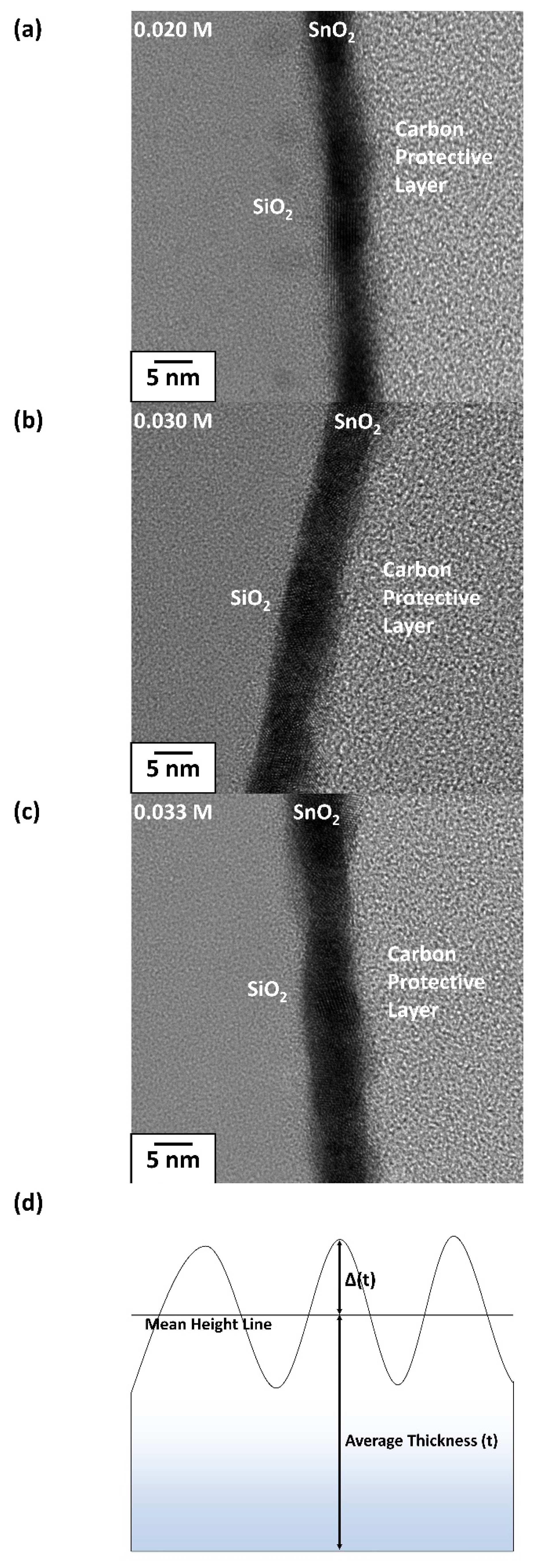
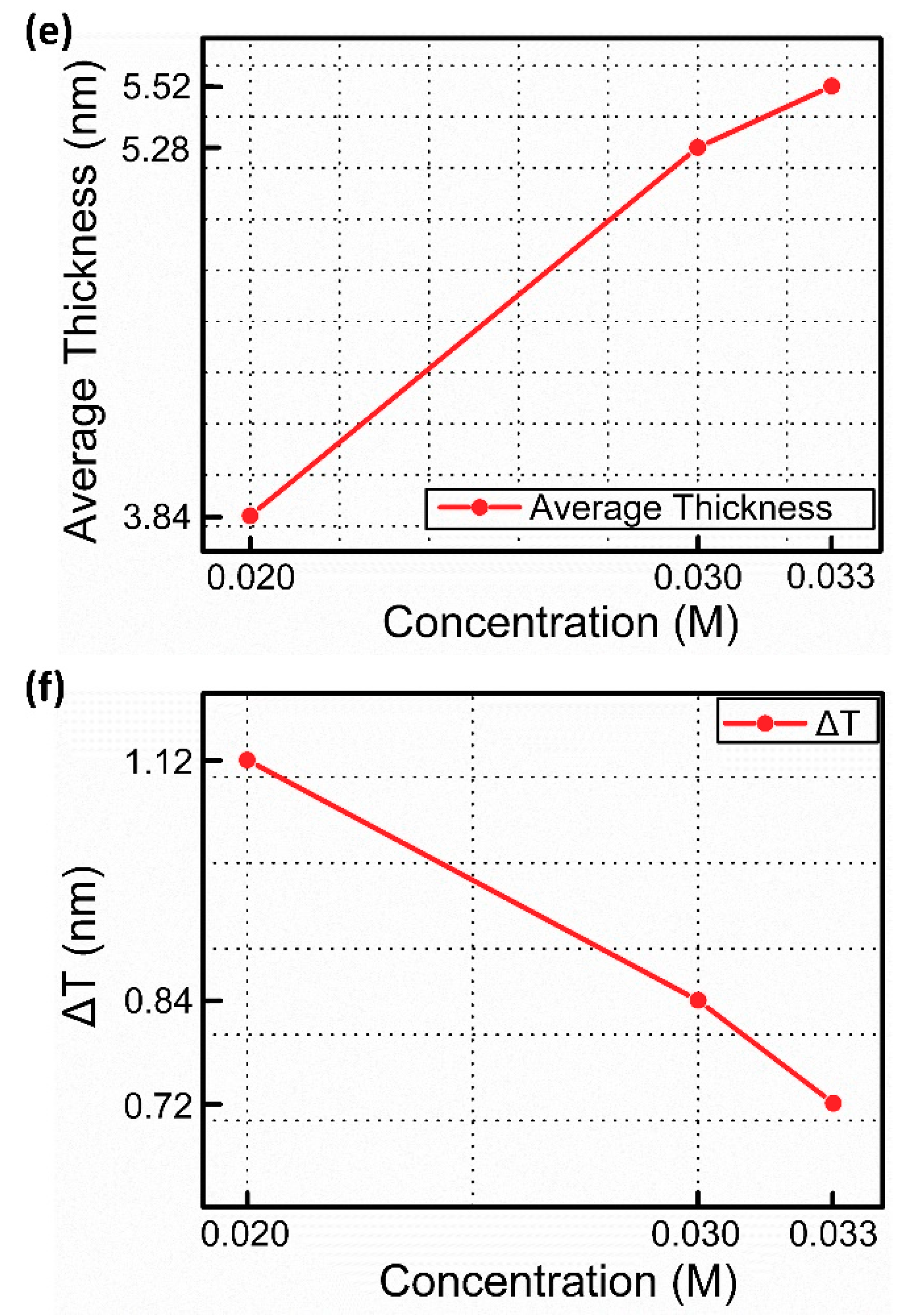
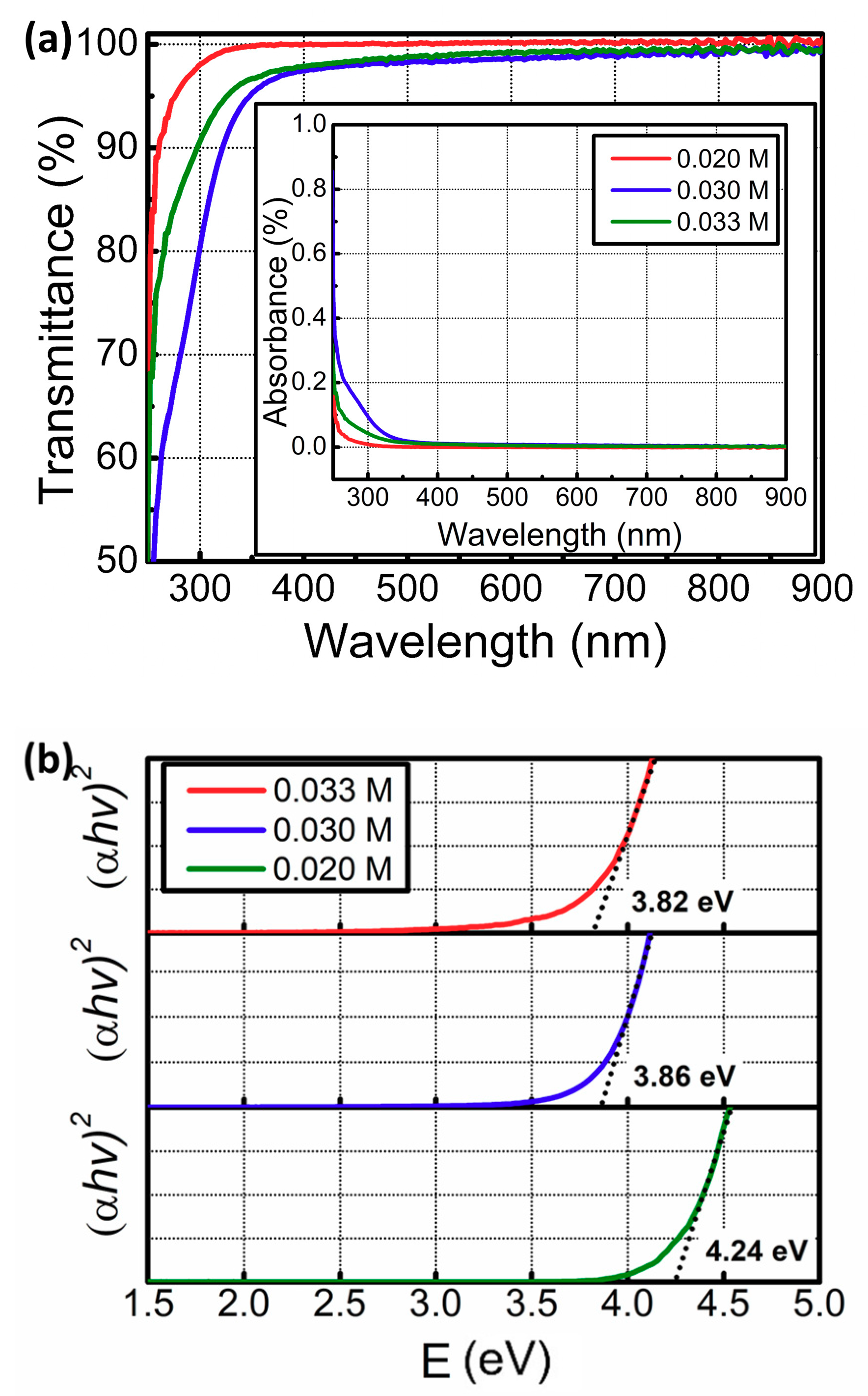
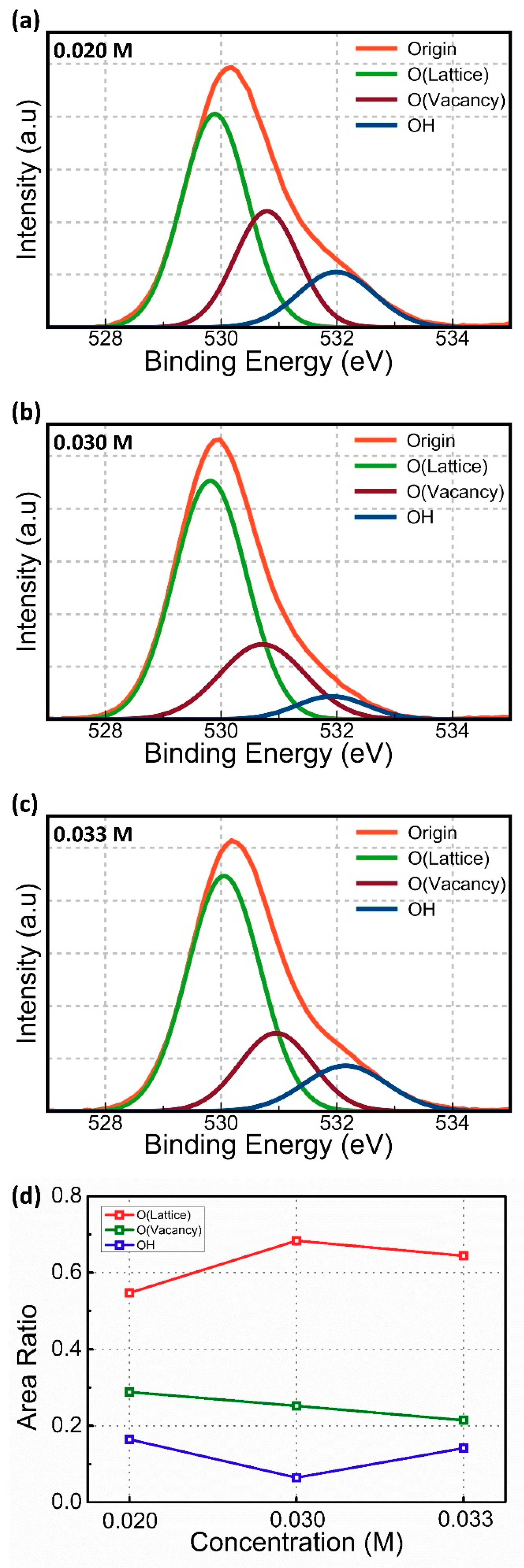
3. Results and Discussion

Figure 1a–c show cross-sectional TEM images of SnO2 films with a carbon protective layer as a function of different precursor concentrations. The estimated film thickness was below 6 nm for all precursor concentrations. All deposited films showed clearly regular atomic spacing, which indicated that the deposited films were in the polycrystalline phase [21]. Figure 1d shows a schematic diagram illustrating the definition of parameters to estimate the film thickness uniformity. The horizontal line through the profile represents the mean height. ΔT was defined as the maximum height of the profile above the mean height line. The estimated T and ΔT values are plotted in Figure 1e,f, respectively. Figure 1e reveals that film thickness increased with the increasing concentration of the precursor, from 0.020 M to 0.033 M. These results are well-matched with the previous report of W. W. Flack et al., who demonstrated that an increase in the concentration of the precursor results in thicker films. Increased concentration leads to an increase in viscosity and convective radical flow [22]. However, in terms of ΔT, thicker films, with higher precursor concentrations, show lower ΔT values, which indicates smooth and uniform film formation.
The optical properties of SnO2 films, as a function of precursor concentration, were investigated by UV-VIS spectroscopy. Figure 2a,b give the transmittance and absorbance spectra, respectively, of SnO2 thin films as a function of precursor concentration. The obtained transmission results for all SnO2 films, ranging from 250 to 900 nm, revealed higher transmittance in the visible range. All SnO2 films showed high transmittance, over 97.0%, in the visible range. These values are adequate for the realization of a solar cell module, which requires over 95% transmittance. The dramatic drop in the ultraviolet regime, around 350 nm, originates from bandgap absorption, which has a value close to the intrinsic bandgap of SnO2 (3.60 eV). The energy band gap values were obtained by extrapolating the line segment in Figure 2c. To extrapolate the line segment, the following equation is used:
( α h ν ) 1 / n = A ( h ν E g ) ,
where α is the absorption coefficient, A is a constant, and Eg is the bandgap of SnO2 films. The value 0.5 (direct transition) is used for the power factor (n). The obtained bandgap values are 4.24 eV, 3.86 eV, and 3.82 eV for 0.020 M, 0.030 M, and 0.033 M, respectively. The value 2 (indirect transition) is used for the power factor (n). The obtained bandgap values are 3.63 eV, 3.28 eV, and 3.15 eV for 0.020 M, 0.030 M, and 0.033 M, respectively. These values are larger than that of bulk SnO2. The increased bandgap with decreasing SnO2 film thickness originates from the quantum confinement effect since the thickness is close to the Bohr radius. It is well known that the Bohr radius of SnO2 is 2.7 nm. The change in energy bandgap can be expected by using the following equation [23,24,25]:
Δ E g = h 2 8 t 2 ( 1 m e * + 1 m h * ) ,
where h is Plank’s constant, t is the film thickness, me* is the effective mass of electrons, and mh* is the effective mass of holes. The calculated bandgap values are 4.23 eV, 3.93 eV, and 3.9 eV, showing a similar trend to the experimentally obtained values of energy quantization. The reduced film thickness affects the physical properties due to the energy quantization phenomena.
XPS analysis of SnO2 thin films as a function of precursor concentrations was conducted to determine the chemical state of the elements. Figure 3a–c show the O1s spectra. All SnO2 films show three components. Three peaks, occurring at 529.8 eV, 530.7 eV, and 531.9 eV corresponded to the oxygen ions (O2−) (OLattice) combined with metal cations, the oxygen vacancy (OVacancy) in the structure, and the hydroxyl groups (-OH), respectively. Figure 3d shows the relative contents of the OLattice, OVacancy, and –OH of SnO2 thin films after the annealing process. As the film thickness is decreased, it is noted that the amount of the oxygen vacancy is increased. Based on the cross-sectional TEM images, the thinnest SnO2 film, made of a low precursor concentration, showed rougher surface characteristics and an increase in air-exposed surface area during the annealing process. It is well known that the increase of the exposure area accelerates the increase of oxygen vacancy formation [26].
Figure 4 shows the representative output curve and transfer curve of the fabricated SnO2 TFTs as a function of precursor concentration. All the fabricated SnO2 TFTs show conventional n-type semiconductor properties. All output curves show a similar tendency, except for the value of drain current. All four graphs exhibit non-linear properties at low drain voltage, indicating that a Schottky contact is formed between the source/drain electrode and the Au electrode. This originates from the high work function of Au [9]. The electrical characteristics of the fabricated SnO2 TFTs were estimated by extracting the representative four parameters, such as field-effect mobility in the saturation regime, subthreshold swing (SS), on/off current ratio, and threshold voltage (Vth). The formulas used for analysis are
I D = μ C i W 2 L ( V G V t h ) 2
and
S S = ( l o g I D V G ) 1
where Ci (insulator capacitance) = 3.45 × 10⁻⁸ F/cm2, W (channel width) = 1000 µm, and L (channel length) = 100 µm. For precursor concentrations of 0.020 M, 0.030 M, and 0.033 M, the field-effect mobilities were 1.01 cm2/Vs, 9.38 cm2/Vs, and 10.83 cm2/Vs, SS values were 2.51 V/decade, 1.99 V/decade, and 1.04 V/decade, and on/off ratios were 1.5 × 10⁶, 4.0 × 10⁷, and 6.7 × 10⁷, respectively. The extracted Vth was 14.9 V, 9.83 V, and −6.77 V for precursor concentrations of 0.020 M, 0.030 M, and 0.033 M, respectively. In order to check the statistical distribution of performance parameters, we compared the extracted parameters of each TFTs (10 devices each). Extracted performance parameters are plotted in Figure 5.
The thicker films showed better performance with respect to field-effect mobility in the saturation regime, on/off current ratio, and SS. The field-effect mobility in the saturation regime increased with increasing precursor concentration. The increased precursor concentration leads to an increase in channel layer thickness. This phenomenon, the relationship between field-effect mobility and active channel thickness, is similar to the results for other metal-oxide and amorphous-silicon-based TFTs. The free carrier concentration per unit accumulation area is proportional to the active channel layer thickness. Thicker films made with higher precursor concentrations have higher free carrier concentrations and show increased film conductivity [27,28]. This results in strong n-type semiconductor properties with high electron carrier concentrations. The increased induced carrier concentration shifts Vth to negative values, causing the transistors to turn on early. In addition, fabricated SnO2 TFTs consisting of thicker channel layers exhibit a lower value of SS. It is well known that the SS values are strongly affected by the trap density (Nt) of the interfaces between the semiconductor and dielectric layers [29] by
N t = [ S S l o g 10 ( e ) k T q 1 ] ( C i q ) ,
where SS is the subthreshold swing, k is Boltzmann’s constant, T is the temperature, q is the electron charge, and Ci is the capacitance of the dielectric layer. The SnO2 TFTs consisting of a thinner channel layer show higher and poorer SS values, indicating the formation of a larger number of trap sites between the semiconductor and dielectric layers. The conductivity and the concentration of trap sites at the surface of the channel layer can be changed by the chemisorption process. It is well known that the adsorption of O2 or H2O molecules on the back-channel of the metal oxide can change device performance. O2 and H2O molecules can capture the electrons from the conduction band and form a depletion region in the back-channel, resulting in a positive Vth shift [30]. The following formulas illustrate the electron capture:
O 2 + e O 2
and
H 2 O + O 2 H 2 O + + O 2 ,
which work as the surface trap center in the back-channel. Even though the chemisorption can be constant, regardless of film thickness, this phenomenon can more dominantly affect thinner films. In addition, the rougher surface of thinner films is more sensitive to this chemisorption, resulting in the degradation of device performance.

4. Conclusions

Sol-gel processed SnO2 TFTs were fabricated on SiO2/p+ Si substrates. The SnO2 active channel layer was deposited by the sol-gel spin coating method. The precursor concentration influenced the film thickness and surface roughness. As the concentration of the precursor was increased, the deposited films were thicker and smoother. It was found that the device performance was influenced by the film thickness and roughness of the SnO2 active channel layer. As the concentration of the precursor was decreased, the fabricated device showed lower field-effect mobility, larger subthreshold swing (SS), and increased threshold voltage (Vth), originating from the lower free carrier concentration and increased trap sites. The fabricated SnO2 TFTs with the optimum precursor concentration of 0.030 M had a field-effect mobility of 9.38 cm2/Vs, a subthreshold swing of 1.99, an Ion/Ioff value of ~4.0 × 10⁷, and showed enhancement mode operation, with positive Vth equal to 9.83 V.

Author Contributions

Conceptualization, D.W.K., H.J.K., and J.J.; Experiments and data analysis, D.W.K., H.J.K., C.L., and K.K.; Investigation, J.-H.B., I.-M.K., and J.J.; Writing—original draft preparation, D.W.K., H.J.K, and J.J.; Writing—Review & Editing, D.W.K., H.J.K., J.-H.B., I.-M.K., and J.J. All authors have read and agreed to the published version of the manuscript.

Funding

This research was supported by the Basic Science Research Program through the National Research Foundation of Korea (NRF) grant funded by the Korea government (MSIT) (2019R1F1A1059788).

Data Availability Statement

Data available in a publicly accessible repository.

Conflicts of Interest

The authors declare no conflict of interest.

References

  1. Kwon, J.-Y.; Lee, D.-J.; Kim, K.-B. Review paper: Transparent amorphous oxide semiconductor thin film transistor. Electron. Mater. Lett. 2011, 7, 1–11. [Google Scholar] [CrossRef]
  2. Nomura, K.; Ohta, H.; Takagi, A.; Kamiya, T.; Hirano, M.; Hosono, H. Room-temperature fabrication of transparent flexible thin-film transistors using amorphous oxide semiconductors. Nat. Cell Biol. 2004, 432, 488–492. [Google Scholar] [CrossRef] [PubMed]
  3. Yabuta, H.; Sano, M.; Abe, K.; Aiba, T.; Den, T.; Kumomi, H.; Nomura, K.; Kamiya, T.; Hosono, H. High-mobility thin-film transistor with amorphous InGaZnO4 channel fabricated by room temperature rf-magnetron sputtering. Appl. Phys. Lett. 2006, 89, 112123. [Google Scholar] [CrossRef]
  4. Tomai, S.; Nishimura, M.; Itose, M.; Matuura, M.; Kasami, M.; Matsuzaki, S.; Kawashima, H.; Utsuno, F.; Yano, K. High performance thin film transistor with amorphous In2O3–SnO2–ZnO channel layer. Jpn. J. Appl. Phys. 2012, 51, 03CB01. [Google Scholar] [CrossRef]
  5. Ebata, K.; Tomai, S.; Tsuruma, Y.; Iitsuka, T.; Matsuzaki, S.; Yano, K. High-Mobility Thin-Film Transistors with Polycrystalline In–Ga–O Channel Fabricated by DC Magnetron Sputtering. Appl. Phys. Express 2012, 5, 011102. [Google Scholar] [CrossRef] [Green Version]
  6. Presley, R.; Munsee, C.L.; Park, C.-H.; Hong, D.; Wager, J.; Keszler, D.A. Tin oxide transparent thin-film transistors. J. Phys. D Appl. Phys. 2004, 37, 2810–2813. [Google Scholar] [CrossRef] [Green Version]
  7. Huang, G.; Duan, L.; Dong, G.; Zhang, D.; Qiu, Y. High-Mobility Solution-Processed Tin Oxide Thin-Film Transistors with High-κ Alumina Dielectric Working in Enhancement Mode. ACS Appl. Mater. Interfaces 2014, 6, 20786–20794. [Google Scholar] [CrossRef]
  8. Jang, J.; Kitsomboonloha, R.; Swisher, S.L.; Park, E.S.; Kang, H.; Subramanian, V. Transparent high-performance thin film transistors from solution-processed SnO2/ZrO2 gel-like precursors. Adv. Mater. 2013, 25, 1042–1047. [Google Scholar] [CrossRef]
  9. Jang, J.; Kang, H.; Chakravarthula, H.C.N.; Subramanian, V. Fully Inkjet-Printed Transparent Oxide Thin Film Transistors Using a Fugitive Wettability Switch. Adv. Electron. Mater. 2015, 1, 1500086. [Google Scholar] [CrossRef]
  10. Jang, B.; Kim, T.; Lee, S.; Lee, W.-Y.; Kang, H.; Cho, C.S.; Jang, J. High performance ultrathin SnO2 thin film transistors by sol-gel method. IEEE Electron. Dev. Lett. 2018, 39, 1179–1182. [Google Scholar]
  11. Jang, B.; Kim, T.; Lee, S.; Lee, W.-Y.; Jang, J. Schottky Nature of Au/SnO2 Ultrathin Film Diode Prepared by Sol-gel Method. IEEE Electron. Dev. Lett. 2018, 39, 1732–1735. [Google Scholar]
  12. Lee, W.Y.; Ha, S.H.; Lee, H.; Bae, J.H.; Jang, B.; Kwon, H.J.; Jang, J. Densification control as a method of improving air stability of thin film transistors based on sol-gel processed SnO2. IEEE Electron. Dev. Lett. 2019, 40, 905–908. [Google Scholar] [CrossRef]
  13. Lee, H.; Ha, S.; Bae, J.-H.; Kang, I.M.; Kim, K.; Lee, W.-Y.; Jang, J. Effect of Annealing Ambient on SnO2 Thin Film Transistors Fabricated via An Ethanol-based Sol-gel Route. Electronics 2019, 8, 955. [Google Scholar] [CrossRef] [Green Version]
  14. Korotcenkov, G.; Orlandi, M.O. Metal Oxides; Series Tin Oxide Materials; Synthesis, Properties, and Applications; Elsevier: Cambridge, MA, USA, 2020. [Google Scholar]
  15. Sun, J.; Lu, A.; Wang, L.; Hu, Y.; Wan, Q. High-mobility transparent thin-film transistors with an Sb-doped SnO2 nanocrystal channel fabricated at room temperature. Nanotechnology 2009, 20, 335204. [Google Scholar] [CrossRef] [PubMed]
  16. Ju, S.; Chen, P.; Zhou, C.; Ha, Y.-G.; Facchetti, A.; Marks, T.J.; Kim, S.K.; Mohammadi, S.; Janes, D.B. 1/f noise of SnO2 nanowire transistors. Appl. Phys. Lett. 2008, 92, 243120. [Google Scholar] [CrossRef] [Green Version]
  17. Ellmer, K. Resistivity of polycrystalline zinc oxide films: current status and physical limit. J. Phys. D Appl. Phys. 2001, 34, 3097–3108. [Google Scholar] [CrossRef]
  18. Fortunato, E.; Barquinha, P.; Pimentel, A.; Pereira, L.; Gonçalves, G.; Martins, R. Amorphous IZO TTFTs with saturation mobilities exceeding 100 cm2/Vs. Phys. Status solidi (RRL)–Rapid Res. Lett. 2006, 1, R34–R36. [Google Scholar] [CrossRef]
  19. Dehuff, N.L.; Kettenring, E.S.; Hong, D.; Chiang, H.Q.; Wager, J.; Hoffman, R.L.; Park, C.-H.; Keszler, D.A. Transparent thin-film transistors with zinc indium oxide channel layer. J. Appl. Phys. 2005, 97, 64505. [Google Scholar] [CrossRef] [Green Version]
  20. Wang, L.; Yoon, M.-H.; Lu, G.; Yang, Y.; Facchetti, A.; Marks, T.J. High-performance transparent inorganic–organic hybrid thin-film n-type transistors. Nat. Mater. 2006, 5, 893–900. [Google Scholar] [CrossRef]
  21. Lee, W.-Y.; Lee, H.; Ha, S.; Lee, C.; Bae, J.-H.; Kang, I.M.; Kim, K.; Jang, J. Effect of Mg Doping on the Electrical Performance of a Sol-Gel-Processed SnO2 Thin-Film Transistor. Electronics 2020, 9, 523. [Google Scholar] [CrossRef] [Green Version]
  22. Shivaraj, B.W.; Narashima Murthy, H.N.; Krishna, M.; Sharma, S.C. Investigation of influence of spin coating parameters on the morphology of ZnO thin films by Taguchi method. Int. J. Thin Film Sci. Technol. 2013, 2, 143–154. [Google Scholar]
  23. Ghosh, S.; Das, K.; Chakrabarti, K.; De, S.K. Effect of oleic acid ligand on photophysical, photoconductive and magnetic properties of monodisperse SnO2 quantum dots. Dalton Trans. 2013, 42, 3434–3446. [Google Scholar] [CrossRef] [PubMed]
  24. Singh, K.C.B.; Vijay, Y.K. Variation of optical band gap in obliquely deposited selenium tin films. Indian J. Pure Appl. Phys. 2005, 43, 129–131. [Google Scholar]
  25. Goh, E.S.M.; Chen, T.P.; Sun, C.Q.; Liu, Y.C. Thickness effect on the bandgap and optical properties of Ge thin films. J. Appl. Phys. 2010, 107, 024305. [Google Scholar] [CrossRef]
  26. Electrical stability of solution-processed a-IGZO TFTs exposed to high-humidity ambient for long periods. IEEE J. Electron Devices Soc. 2019, 7, 26–32.
  27. Park, J.S.; Jeong, J.K.; Mo, Y.G.; Kim, D.H.; Kim, C. Control of threshold voltage in ZnO-based oxide thin film transistor. J. Appl. Phys. Lett. 2008, 93, 033513. [Google Scholar] [CrossRef]
  28. Lee, S.Y.; Kim, D.H.; Chong, E.Y.; Jeon, W.; Kim, D.H. Effect of channel thickness on density of states in amorphous InGaZnO thin film transistor. Appl. Phys. Lett. 2011, 98, 122105. [Google Scholar] [CrossRef] [Green Version]
  29. Rolland, A.; Richard, J.; Kleider, J.P.; Mencaraglia, D. Electrical Properties of Amorphous Silicon Transistors and MIS-Devices: Comparative Study of Top Nitride and Bottom Nitride Configurations. J. Electrochem. Soc. 1993, 140, 3679–3683. [Google Scholar] [CrossRef]
  30. Yapabandara, K.; Mirkhani, V.; Sultan, M.S.; Ozden, B.; Khanal, M.P.; Park, M.; Wang, S.; Hamilton, M.C.; Chung, Y.; Kim, N.-J.; et al. Study of device instability of bottom-gate ZnO transistors with sol–gel derived channel layers. J. Vac. Sci. Technol. B 2017, 35, 03D104. [Google Scholar] [CrossRef]
Figure 1. (ac) Cross-sectional TEM images of 0.020, 0.030, and 0.033 M SnO2 films, respectively. (d) Schematic diagram illustrating the definition of parameters and estimated (e) average thickness and (f) ΔT parameters.
Electronics 10 00200 g001aElectronics 10 00200 g001b
Figure 2. (a) Transmittance of the prepared SnO2 films; the inset shows absorbance spectra. (b) (ahv)2 vs. photon energy and (c) (ahv)0.5 vs. photon energy for prepared SnO2 films. (d) Energy bandgap as a function of the precursor concentrations.
Electronics 10 00200 g002aElectronics 10 00200 g002b
Figure 3. (ac) O1s XPS spectra of SnO2 thin films and (d) O1s composition as a function of precursor concentrations.
Electronics 10 00200 g003
Figure 4. (ac) ID-VD curves and (d) transfer curves of SnO2 thin-film transistors as a function of precursor concentrations.
Electronics 10 00200 g004aElectronics 10 00200 g004b
Figure 5. Extracted thin-film transistor performance parameters: (a) field-effect mobility in saturation regime, (b) subthreshold swing (SS), (c) Vth, and (d) Ion and Ioff.
Electronics 10 00200 g005aElectronics 10 00200 g005b
Publisher’s Note: MDPI stays neutral with regard to jurisdictional claims in published maps and institutional affiliations.

