
Transparent All-Oxide Hybrid NiO:N/TiO2 Heterostructure for Optoelectronic Applications

 ,
,
Abstract
:1. Introduction
2. Materials and Methods
2.1. Thin Films Deposition
2.1.1. NiO Films Preparation
2.1.2. TiO2 Films Preparation
2.2. Fabrication of NiO:N/TiO2Heterojunction
2.3. Thin Films and Device Characterization
3. Results and Discussion
3.1. Thin Films Properties
3.1.1. Properties of NiO and NiO:NThin Films
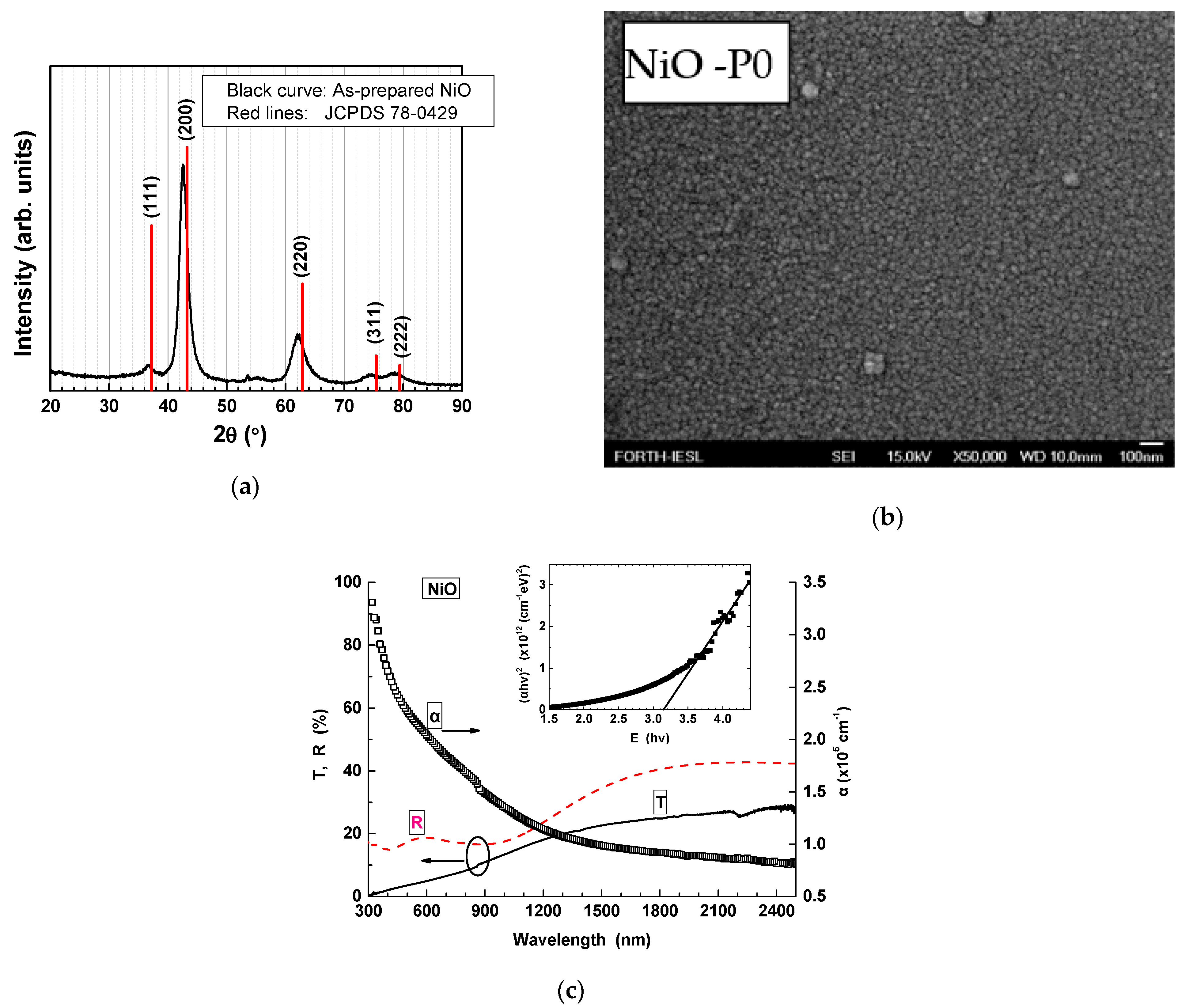
NiO Thin Films
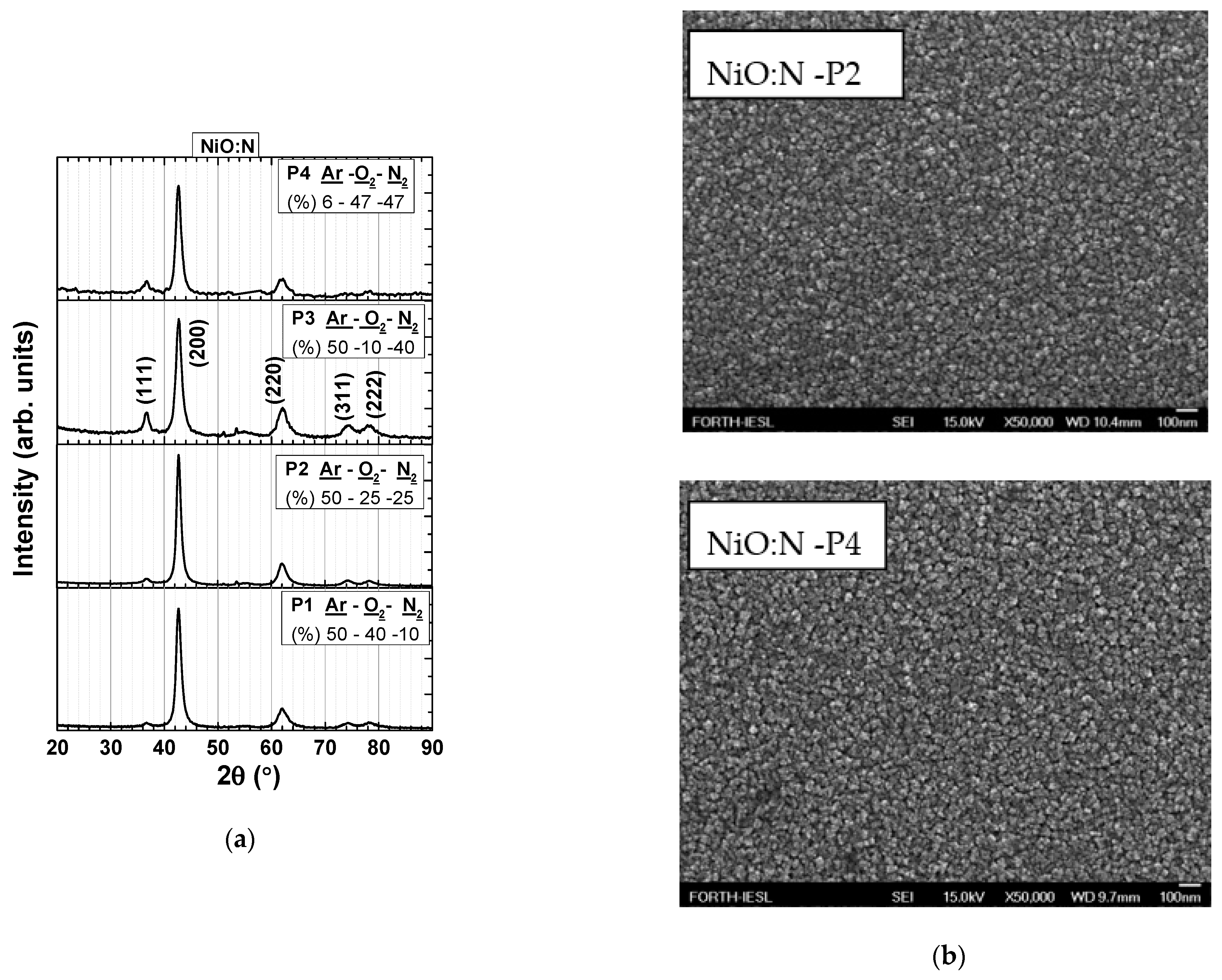
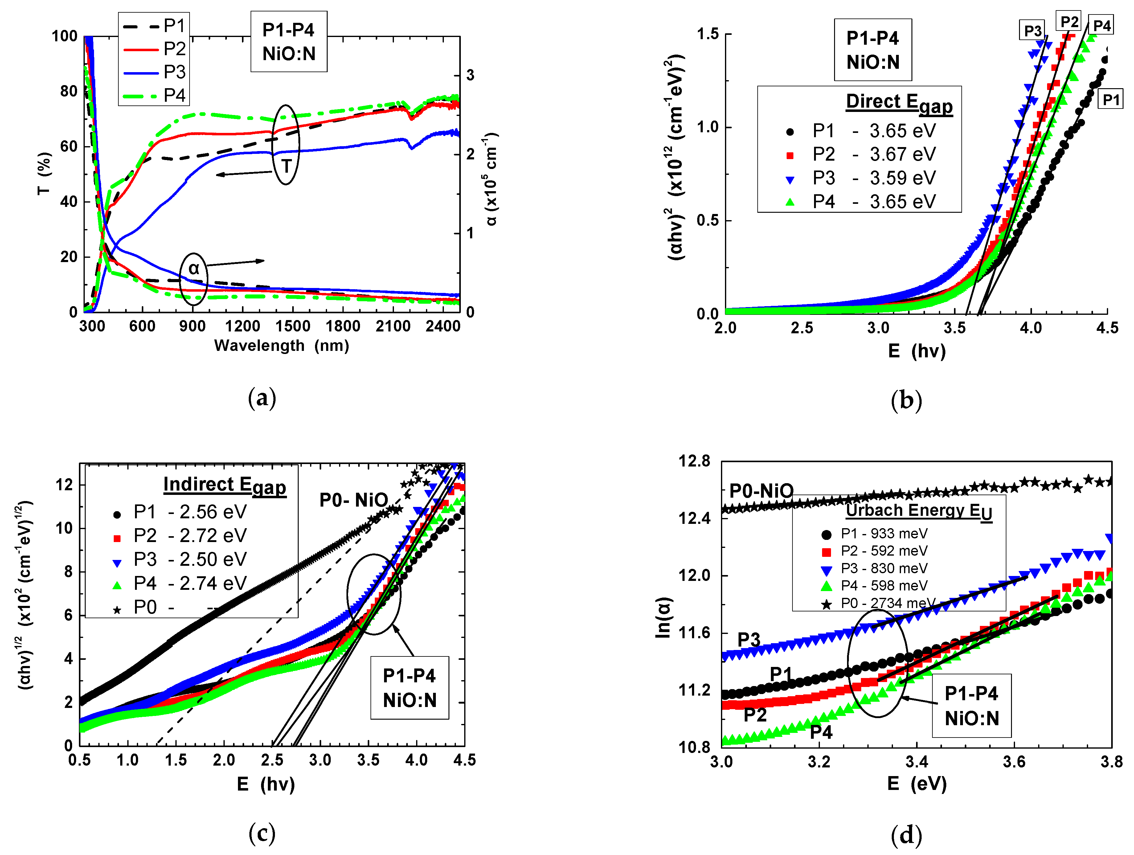
NiO:N Thin Films
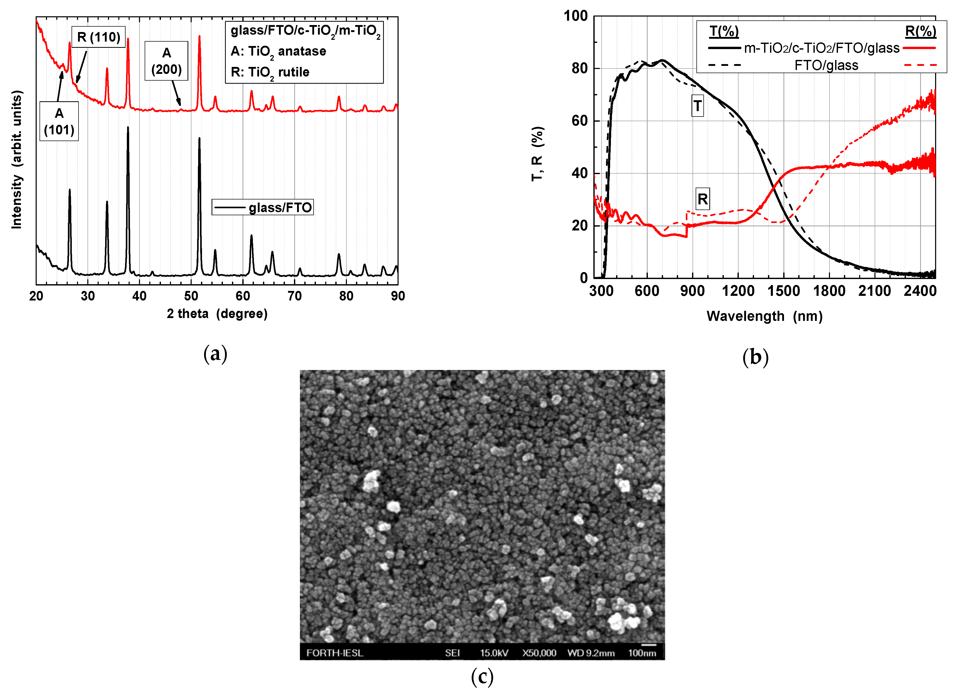
3.1.2. Properties of TiO2Thin Film
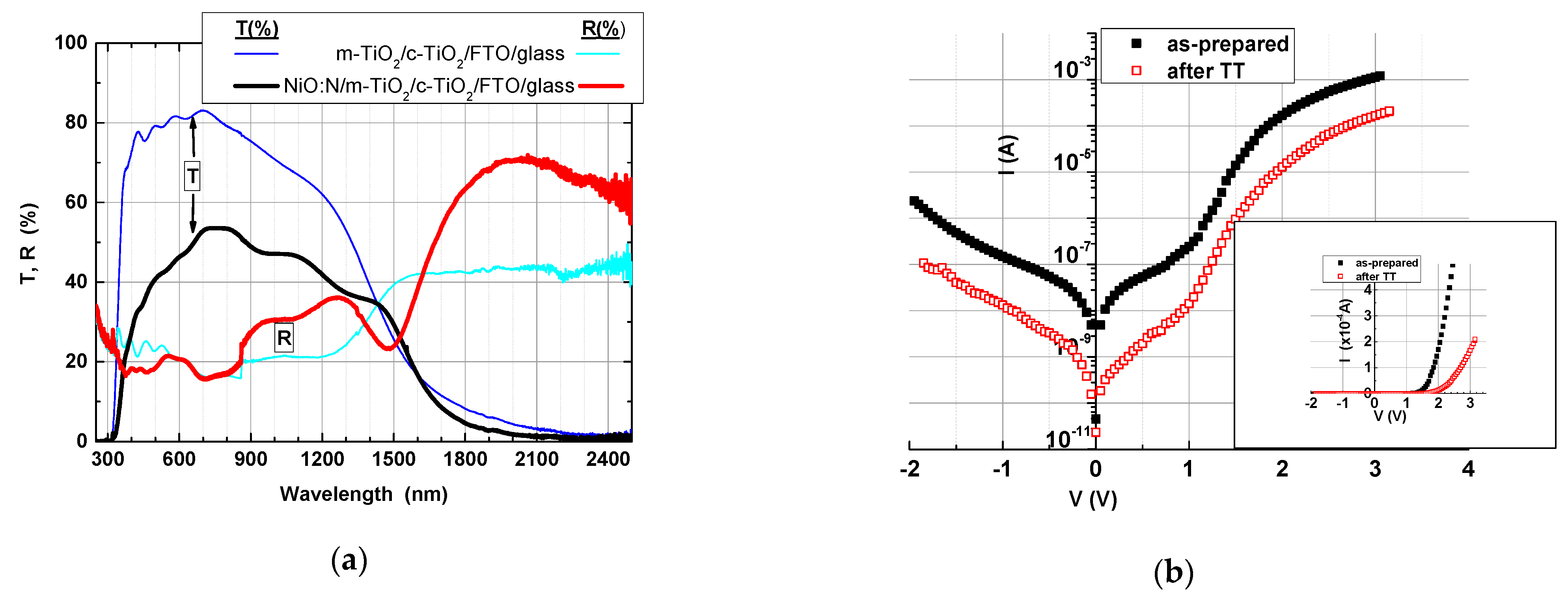
3.2. Characterization of the p-NiO:N/n-TiO2Diode
4. Conclusions
Supplementary Materials
Author Contributions
Funding
Data Availability Statement
Conflicts of Interest
References
- Osorio-Guillén, J.; Lany, S.; Zunger, A. Nonstoichiometry and hole doping in NiO. AIP Conf. Proc. 2010, 1199, 128–129. [Google Scholar] [CrossRef] [Green Version]
- Karsthof, R.; Grundmann, M.; Anton, A.M.; Kremer, F. Polaronic interacceptor hopping transport in intrinsically doped nickel oxide. Phys. Rev. B 2019, 99, 235201. [Google Scholar] [CrossRef] [Green Version]
- Zou, Z.G.; Ye, J.H.; Sayama, K.; Arakawa, H. Direct splitting of water under visible light irradiation with an oxide semiconductor photocatalyst. Nature 2001, 414, 625–627. [Google Scholar] [CrossRef]
- Charisiadis, A.; Glymenaki, E.; Planchat, A.; Margiola, S.; Lavergne-Bril, A.-C.; Nikoloudakis, E.; Nikolaou, V.; Charalambidis, G.; Coutsolelos, A.G.; Odobel, F. Photoelectrochemical properties of dyads composed of porphyrin/ruthenium catalyst grafted on metal oxide semiconductors. Dye. Pigment. 2021, 185, 108908. [Google Scholar] [CrossRef]
- Rosado, P.C.; Meyrelles, R.; Macatrão, A.M.; Justino, M.C.; Gomes, A.G.; Montemor, M.F.; Alves, M.M.; Justino, G.C.; Ribeiro, A.P.C.; Shimizu, K. Immobilization of His-tagged proteins on NiO foams for recyclable enzymatic reactors. Appl. Sur. Sci. 2021, 537, 147848. [Google Scholar] [CrossRef]
- Dey, S.; Nag, S.; Santra, S.; Ray, S.K.; Guha, P.K. Voltage-controlled NiO/ZnO p–n heterojunction diode: A new approach towards selective VOC sensing. Microsyst. Nanoeng. 2020, 6, 35. [Google Scholar] [CrossRef]
- Gagaoudakis, E.; Michail, G.; Kampylafka, V.; Tsagaraki, K.; Aperathitis, E.; Moschovis, K.; Binas, V.; Kiriakidis, G. Room Temperature p-Type NiO Nanostructure Thin Film Sensor for Hydrogen and Methane Detection. Sens. Lett. 2017, 15, 663–667. [Google Scholar] [CrossRef]
- Zhang, J.; Yu, A. Nanostructured transition metal oxides as advanced anodes for lithium-ion batteries. Sci. Bull. 2015, 60, 823–838. [Google Scholar] [CrossRef] [Green Version]
- Wang, Z.; Wang, X.; Cong, S.; Geng, F.; Zhao, Z. Fusing electrochromic technology with other advanced technologies: A new roadmap for future development. Mat. Sci. Eng. R 2020, 140, 100524. [Google Scholar] [CrossRef]
- Patel, M.; Kim, H.-S.; Park, H.-H.; Kim, J. Active Adoption of Void Formation in Metal-Oxide for All Transparent Super-Performing Photodetectors. Sci. Rep. 2016, 6, 25461. [Google Scholar] [CrossRef] [Green Version]
- Karsthof, R.; von Wenckstern, H.; Zúniga-Pérez, J.; Deparis, C.; Grundmann, M. Nickel Oxide–Based Heterostructures with Large Band Offsets. Phys. Status Solidi B 2020, 257, 1900639. [Google Scholar] [CrossRef]
- Grundmann, M.; Klüpfel, F.; Karsthof, R.; Schlupp, P.; Schein, F.-L.; Splith, D.; Yang, C.; Bitter, S.; von Wenckstern, H. Oxide bipolar electronics: Materials, devices and circuits. J. Phys. D Appl. Phys. 2016, 49, 213001. [Google Scholar] [CrossRef]
- Tirado, J.; Vásquez-Montoya, M.; Roldán-Carmona, C.; Ralaiarisoa, M.; Koch, N.; Nazeeruddin, M.K.; Jaramillo, F. Air-Stable n–i–p Planar Perovskite Solar Cells Using Nickel Oxide Nanocrystals as Sole Hole-Transporting Material. ACS Appl. Energy Mater. 2019, 2, 4890–4899. [Google Scholar] [CrossRef]
- Elseman, A.M.; Sajid, S.; Shalan, A.E.; Mohamed, S.A.; Rashad, M.M. Recent progress concerning inorganic hole transport layers for efficient perovskite solar cells. Appl. Phys. A 2019, 125, 476. [Google Scholar] [CrossRef]
- Predanocy, M.; Hotovy, I.; Caplovicová, M. Structural optical and electrical properties of sputtered NiO thin films for gas detection. Appl. Surf. Sci. 2017, 395, 208–213. [Google Scholar] [CrossRef]
- Yang, J.-L.; Lai, Y.-S.; Chen, J.S. Effect of heat treatment on the properties of non-stoichiometric p-type nickel oxide films deposited by reactive sputtering. Thin Solid Film 2005, 488, 242–246. [Google Scholar] [CrossRef]
- Hwang, J.D.; Ho, T.H. Effects of oxygen content on the structural, optical, and electrical properties of NiO films fabricated by radio-frequency magnetron sputtering. Mat. Sci. Semicond. Process. 2017, 71, 396–400. [Google Scholar] [CrossRef]
- Nandy, S.; Saha, B.; Mitra, M.K.; Chattopadhyay, K.K. Effect of oxygen partial pressure on the electrical and optical properties of highly (200) oriented p-type Ni1–xO films by DC sputtering. J. Mater. Sci. 2007, 42, 5766–5772. [Google Scholar] [CrossRef]
- Nolan, M.; Long, R.; English, N.J.; Mooney, D.A. Hybrid density functional theory description of N- and C-doping of NiO. J. Chem. Phys. 2011, 134, 224703. [Google Scholar] [CrossRef] [Green Version]
- Zhang, L.; Staar, P.; Kozhevnikov, A.; Wang, Y.-P.; Trinastic, J.; Schulthess, T. DFT + DMFT calculations of the complex band and tunneling behavior for the transition metal monoxides MnO, FeO, CoO, and NiO. Phys. Rev. B 2019, 100, 035104. [Google Scholar] [CrossRef] [Green Version]
- Kim, D.S.; Lee, H.C. Nickel vacancy behavior in the electrical conductance of non-stoichiometric nickel oxide film. J. Appl. Phys. 2012, 112, 034504. [Google Scholar] [CrossRef]
- Zhang, K.H.L.; Xi, K.; Blamire, M.G.; Egdell, R.G. P-type transparent conducting oxides. J. Phys. Condens. Matter 2016, 28, 383002. [Google Scholar] [CrossRef] [PubMed]
- Uddin, M.T.; Nicolas, Y.; Olivier, C.; Jaegermann, W.; Rockstroh, N.; Junge, H.; Toupance, T. “Band alignment investigations of heterostructures NiO/TiO2 nanomaterials used as efficient heterojunction earth-abundant metal oxide photocatalysts for hydrogen production. Phys. Chem. Chem. Phys. 2017, 19, 19279–19288. [Google Scholar] [CrossRef] [PubMed]
- Nguyen, T.T.; Patel, M.; Kim, J. All-inorganic metal oxide transparent solar cells. Sol. Energy Mater. Sol. Cells 2020, 217, 110708. [Google Scholar] [CrossRef]
- Klochko, N.P.; Kopach, V.R.; Tyukhov, I.I.; Zhadan, D.O.; Klepikova, K.S.; Khrypunova, G.S.; Petrushenko, S.I.; Lyubov, V.M.; Kirichenko, M.V.; Dukarov, S.V.; et al. Metal oxide heterojunction (NiO/ZnO) prepared by low temperature solution growth for UV-photodetector and semi-transparent solar cell. Sol. Energy 2018, 164, 149–159. [Google Scholar] [CrossRef]
- Gong, H.H.; Chen, X.H.; Xu, Y.; Ren, F.-F.; Gu, S.L.; Ye, J.D. A 1.86-kV double-layered NiO/β-Ga2O3 vertical p–n heterojunction diode. Appl. Phys. Lett. 2020, 117, 022104. [Google Scholar] [CrossRef]
- Wu, C.-C.; Yang, C.-F. Effect of annealing temperature on the characteristics of the modified spray deposited Li-doped NiO films and their applications in transparent heterojunction diode. Sol. Energy Mater. Sol. Cells 2015, 132, 492–498. [Google Scholar] [CrossRef]
- Nandy, S.; Maiti, U.N.; Ghosh, C.K.; Chattopadhyay, K.K. Enhanced p-type conductivity and band gap narrowing in heavily Al doped NiO thin films deposited by RF magnetron sputtering. J. Phys. Condens. Matter 2009, 21, 115804. [Google Scholar] [CrossRef]
- Adler, D.; Feinleib, J. Electrical and Optical Properties of Narrow-Band Materials. Phys. Rev. B 1970, 2, 3112–3134. [Google Scholar] [CrossRef]
- Park, S.G.; Lee, K.H.; Lee, J.-H.; Bang, G.; Kim, J.; Park, H.J.; Oh, M.S.; Lee, S.; Kim, Y.-H.; Kim, Y.-M.; et al. Improved polaronic transport under a strong Mott–Hubbard interaction in Cu substituted NiO. Inorg. Chem. Front. 2020, 7, 853–858. [Google Scholar] [CrossRef]
- Popescu, I.; Skoufa, Z.; Heracleous, E.; Lemonidou, A.; Marcu, I.-C. A study by electrical conductivity measurements of the semiconductive and redox properties of Nb-doped NiO catalysts in correlation with the oxidative dehydrogenation of ethane. Phys. Chem. Chem. Phys. 2015, 17, 8138–8147. [Google Scholar] [CrossRef] [PubMed]
- Keraudy, J.; Ferrec, A.; Richard-Plouet, M.; Hamon, J.; Goullet, A.; Jouan, P.-Y. Nitrogen doping on NiO by reactive magnetron sputtering: A new pathway to dynamically tune the optical and electrical properties. Appl. Surf. Sci. 2017, 409, 77–84. [Google Scholar] [CrossRef]
- Tangwancharoen, S.; Thongbai, P.; Yamwong, T.; Maensiri, S. Dielectric and electrical properties of giant dielectric (Li, Al)-doped NiO ceramics. Mat. Chem. Phys. 2009, 115, 585–589. [Google Scholar] [CrossRef]
- Dong, D.; Wang, W.; Barnabe, A.; Presmanes, L.; Rougier, A.; Dong, G.; Zhang, F.; Yu, H.; He, Y.; Dia, X. Enhanced electrochromism in short wavelengths for NiO:(Li, Mg) films in full inorganic device ITO/NiO:(Li, Mg)/Ta2O5/WO3/ITO. Electrochim. Acta 2018, 263, 277–285. [Google Scholar] [CrossRef] [Green Version]
- Wen, C.-K.; Xin, Y.-Q.; Chen, S.-C.; Chuang, T.-H.; Chen, P.-J.; Sun, H. Comparison of microstructural and optoelectronic properties of NiO:Cu thin films deposited by ion-beam assisted rf sputtering in different gas atmospheres. Thin Solid Film. 2019, 677, 103–108. [Google Scholar] [CrossRef]
- Wrobel, F.; Park, H.; Sohn, C.; Hsiao, H.-W.; Zuo, J.-M.; Shin, H.; Lee, H.N.; Ganesh, P.; Benali, A.P.; Kent, R.C.; et al. Doped NiO: The mottness of a charge transfer insulator. Phys. Rev. B 2020, 101, 195128. [Google Scholar] [CrossRef]
- Ganesh, V.; Haritha, L.; Anisc, M.; Shkira, M.; Yahia, I.S.; Singh, A.; AlFaify, S. Structural, morphological, optical and third order nonlinear optical response of spin-coated NiO thin films: An effect of N doping. Solid State Sci. 2018, 86, 98–106. [Google Scholar] [CrossRef]
- Sriram, S.; Thayumanavan, A.; Ravichandran, K. Influence of nitrogen doping on properties of NiO films. Surf. Eng. 2016, 32, 207–211. [Google Scholar] [CrossRef]
- Zhou, P.; Li, B.; Fang, Z.; Zhou, W.; Zhang, M.; Hu, W.; Chen, T.; Xiao, Z.; Yang, S. Nitrogen-Doped Nickel Oxide as Hole Transport Layer for High-Efficiency Inverted Planar Perovskite Solar Cells. Sol. RRL 2019, 3, 1900164. [Google Scholar] [CrossRef]
- Tian, Y.; Gong, L.; Qi, X.; Yang, Y.; Zhao, X. Effect of Substrate Temperature on the Optical and Electrical Properties of Nitrogen-Doped NiO Thin Films. Coatings 2019, 9, 634. [Google Scholar] [CrossRef] [Green Version]
- Aftab, M.; Butt, M.Z.; Ali, D.; Bashir, F.; Aftab, Z.H. Impact of copper doping in NiO thin films on their structure, morphology, and antibacterial activity against Escherichia Coli. Ceram. Int. 2020, 46, 5037–5049. [Google Scholar] [CrossRef]
- Pankove, J. Optical Processes in Semiconductors; Dover Publications: Mineola, NY, USA, 1971; Chapter 4; p. 87. [Google Scholar]
- Jafar, M.M.A.G. Comprehensive formulations for the total normal-incidence optical reflectance and transmittance of thin films laid on thick substrates. Eur. Int. J. Sci. Technol. 2013, 2, 214–274. Available online: www.cekinfo.org.uk/EIJST (accessed on 28 August 2016).
- Siddique, M.N.; Ahmed, A.; Tripathi, P. Enhanced optical properties of pure and Sr doped NiO nanostructures: A comprehensive study. Optik 2019, 185, 599–608. [Google Scholar] [CrossRef]
- Lin, C.-W.; Chung, W.-C.; Zhang, Z.-D.; Hsu, M.-C. P-channel transparent thin-film transistor using physical-vapor-deposited NiO layer. Jpn. J. Appl. Phys. 2018, 57, 01AE01. [Google Scholar] [CrossRef] [Green Version]
- Davis, E.A.; Mott, N.F. Conduction in non-crystalline systems V. Conductivity, optical absorption and photoconductivity in amorphous semiconductors. Philos. Mag. 1970, 22, 0903–0922. [Google Scholar] [CrossRef]
- Chopra, K.L.; Bahlt, S.K. Exponential tail of the optical absorption edge of amorphous semiconductors. Thin Solid Film. 1972, I1, 377–388. [Google Scholar] [CrossRef]
- Choudhury, B.; Choudhury, A. Oxygen defect dependent variation of band gap, Urbach energy and luminescence property of anatase, anatase–rutile mixed phase and of rutile phases of TiO2 nanoparticles. Phys. E 2014, 56, 364–371. [Google Scholar] [CrossRef]
- Akshay, V.R.; Arun, B.; Mandal, G.; Vasundhara, M. Visible range optical absorption, Urbach energy estimation and paramagnetic response in Cr-doped TiO2 nanocrystals derived by a sol–gel method. Phys. Chem. Chem. Phys. 2019, 21, 12991–13004. [Google Scholar] [CrossRef]
- Klochko, N.P.; Klepikova, K.S.; Kopach, V.R.; Khrypunov, G.S.; Myagchenko, Y.O.; Melnychuk, E.E.; Lyubov, V.M.; Kopach, A.V. On Controlling the Hydrophobicity of Nanostructured Zinc-Oxide Layers Grown by Pulsed Electrodeposition. Semiconductors 2016, 50, 352–363. [Google Scholar] [CrossRef]
- Anyaegbunam, F.N.C.; Augustine, C. A Study of Optical Band Gap and Associated Urbach Energy Tail of Chemically Deposited Metal Oxides Binary Thin Films. Dig. J. Nanomater. Biostruct. 2018, 13, 847–856. [Google Scholar]
- Biswas, D.; Das, A.S.; Mondal, R.; Banerjee, A.; Dutta, A.; Kabi, S.; Roy, D.; Singh, L.S. Structural properties and electrical conductivity mechanisms of semiconducting quaternary nanocomposites: Effect of two transition metal oxides. J. Phys. Chem. 2020, 144, 109505. [Google Scholar] [CrossRef]
- Sharma, N.; Prabakar, K.; Ilango, S.; Dash, S.; Tyagi, A.K. Optical band-gap and associated Urbach energy tails in defected AlN thin films grown by ion beam sputter deposition: Effect of assisted ion energy. Adv. Mat. Proc. 2017, 2, 342–346. [Google Scholar] [CrossRef] [Green Version]
- Hassanien, A.S.; Akl, A.A. Effect of Se addition on optical and electrical properties of chalcogenideCdSSe thin films. Superlattices Microstruct. 2016, 89, 153–169. [Google Scholar] [CrossRef]
- Kozlova, S.G.; Ryzhikov, M.R.; Shayapov, V.R.; Samsonenko, D.G. Effect of spin–phonon interactions on Urbach tails in flexible [M2(bdc)2(dabco)]. Phys. Chem. Chem. Phys. 2020, 22, 15242–15247. [Google Scholar] [CrossRef]
- De Wolf, S.; Holovsky, J.; Moon, S.J.; Lopper, P.; Niesen, B.; Ledinsky, M.; Haug, F.J.; Yum, J.H.; Ballif, C. Organometallic Halide Perovskites: Sharp Optical Absorption Edge and Its Relation to Photovoltaic Performance. J. Phys. Chem. Lett. 2014, 5, 1035–1039. [Google Scholar] [CrossRef]
- Ishikawa, R.; Kato, T.; Anzo, R.; Nagatake, M.; Nishimura, T.; Tsuboi, N.; Miyajima, S. Widegap CH3NH3PbBr3 solar cells for optical wireless power transmission application. Appl. Phys. Lett. 2020, 117, 013902. [Google Scholar] [CrossRef]
- Al Boukhari, J.; Zeidan, L.; Khalaf, A.; Awad, R. Synthesis, characterization, optical and magnetic properties of pure and Mn, Fe and Zn doped NiO nanoparticles. Chem. Phys. 2019, 516, 116–124. [Google Scholar] [CrossRef]
- Maiti, S.; van der Laan, M.; Poonia, D.; Schall, P.; Kinge, S.; Siebbeles, L.D.A. Emergence of new materials for exploiting highly efficient carrier multiplication in photovoltaics. Chem. Phys. Rev. 2020, 1, 011302. [Google Scholar] [CrossRef]
- Aperathitis, E.; Bender, M.; Cimalla, V.; Ecke, G.; Modreanu, M. Properties of rf-sputtered indium–tin-oxynitride thin films. J. Appl. Phys. 2003, 94, 1258–1266. [Google Scholar] [CrossRef]
- Gong, H.; Chen, X.; Xu, Y.; Chen, Y.; Ren, F.; Liu, B.; Gu, S.; Zhang, R.; Ye, J. Band Alignment and Interface Recombination inNiO/β-Ga2O3 Type-II p-n Heterojunctions. IEEE Trans. Electron. Devices 2020, 67, 3341–3347. [Google Scholar] [CrossRef]
- Abbas, S.; Kim, J. All-metal oxide transparent photodetector for broad responses. Sens. Actuators A 2020, 303, 111835. [Google Scholar] [CrossRef]
- Egbo, K.O.; Kong, M.; Liu, C.P.; Yu, K.M. Room temperature sputtered Cu doped NiO1+δ: P-type conductivity, stability of electrical properties and p-n heterojunction. J. Alloys Compd. 2020, 835, 155269. [Google Scholar] [CrossRef]
- Lin, F.; Gillaspie, D.T.; Dillon, A.C.; Richards, R.M.; Engtrakul, C. Nitrogen-doped nickel oxide thin films for enhanced electrochromic applications. Thin Solid Film 2013, 527, 26–30. [Google Scholar] [CrossRef]
- Gagaoudakis, E.; Aperathitis, E.; Michail, G.; Kiriakidis, G.; Binas, V. Sputtered VO2 coatings on commercial glass substrates for smart glazing applications. Sol. Energy Mater. Sol. Cells 2021, 220, 110845. [Google Scholar] [CrossRef]
- Sze, S.M. Physics of Semiconductor Devices, 2nd ed.; John Wiley and Sons Ltd: Hoboken, NJ, USA, 1981; ISBN 978-0471098379. [Google Scholar]
- Cheung, S.K.; Cheung, N.W. Extraction of Schottky diode parameters from forward current-voltage characteristics. Appl. Phys. Lett. 1986, 49, 85–87. [Google Scholar] [CrossRef]
- Robinson, G.Y. Schottky Diodes and Ohmic Contacts for the III-V Semiconductors. In Physics and Chemistry of III—V Compound Semiconductor Interfaces; Wilmsen, C.W., Ed.; Springer: Boston, MA, USA, 1985. [Google Scholar] [CrossRef]
- Schroder, D.K. Semiconductor Material and Device Characterization, 3rd ed.; John Wiley Sons: Hoboken, NJ, USA, 2006; ISBN 978-0-471-73906-7. [Google Scholar]
- Al-Ahmadi, N.A.; Ebrahim, F.A.; Al-Jawhari, H.A.; Mari, R.H.; Henini, M. Impact of doping on the performance of p-type Be-doped Al0.29Ga0.71As Schottky diodes. Mod. Electron. Mater. 2017, 3, 66–71. [Google Scholar] [CrossRef]
- Hasan, M.R.; Xie, T.; Barron, S.C.; Liu, G.; Nguyen, N.V.; Motayed, A.; Rao, M.V.; Debnath, R. Self-powered p-NiO/n-ZnO heterojunction ultraviolet photodetectors fabricated on plastic substrates. APL Mater. 2015, 3, 106101. [Google Scholar] [CrossRef] [PubMed]


| Depos. Techn. | Tsub (°C) | D (nm) | TT | Optical Properties TVIS/Egap Direct (Egap Indirect) | Resistivity or Resistance | Ref. | |
|---|---|---|---|---|---|---|---|
| Chemical solution | 280 | 10 | - | NiO | - | 7.1 MΩcm | [39] |
| NiO:N | 80–82%/- | 4.8 MΩcm | |||||
| Sol-gel | 120 | 200 | 450 °C 1 h | NiO | ~70%/4 eV (3.5 eV) | - | [37] |
| NiO:N | 50–70%/3.8 eV (3.25 eV) | - | |||||
| Spray techn. | 350 | 720–900 | NiO | ~40–60%/3.5 eV (3.41 eV) | 3.8 kΩcm | [38] | |
| NiO:N | 30–50%/3.45 eV | 1.7 kΩcm | |||||
| RF MS | 100–400 | 300 | - | NiO | ~90%/3.53 eV | 28.3 Ω | [40] |
| NiO:N | 90%/3.5 eV | 28 Ω | |||||
| DC MS | RT | 300 | NiO: | ~30–40%/3.6 eV | - | [32] | |
| NiO:N | <40%/3.3 eV (2.3 eV) | - | |||||
| RF S | RT | ~150 | NiO | ~7%/3.15 eV | 23 kΩ | This work | |
| NiO:N | 45–70%/3.67 eV (2.72 eV) | >100 kΩ | |||||
| Films | Deposition Parameters | Structural Properties | Optical Properties | ||||||||||
|---|---|---|---|---|---|---|---|---|---|---|---|---|---|
| Flow Rates (%) | d (nm) | D. R. (nm/min) | 2θ (Degree) | D (nm) | εL (×10−2) | T (%) (@550 nm) | Direct Egap (eV) | Indirect Egap (eV) | EU (meV) | ||||
| Ar | O2 | N2 | |||||||||||
| NiO | P0 | 50 | 50 | 0 | 144 | 1.06 | 42.58 | 5.24 | 1.78 | 4.2 | 3.15 | - | 2734 |
| NiO:N | P1 | 50 | 40 | 10 | 128 | 1.52 | 42.65 | 6.15 | 1.20 | 51.7 | 3.65 | 2.56 | 933 |
| P2 | 50 | 25 | 25 | 133 | 1.05 | 42.71 | 9.14 | 1.15 | 49.1 | 3.67 | 2.72 | 592 | |
| P3 | 50 | 10 | 40 | 159 | 0.94 | 42.70 | 6.69 | 1.32 | 29.3 | 3.59 | 2.50 | 830 | |
| P4 | 6 | 47 | 47 | 142 | 0.64 | 42.64 | 7.16 | 1.39 | 51.2 | 3.65 | 2.74 | 598 | |
| JS (A) | RS (Ohm) | n | Φb (eV) | |||||
|---|---|---|---|---|---|---|---|---|
| Before TT | After TT | Before TT | After TT | Before TT | After TT | Before TT | After TT | |
| I–V method | 5.0 × 10⁻⁹ | 2.8 × 10⁻¹⁰ | 8.5 × 10² | 1.4 × 10⁴ | 4.6 | 4.4 | 0.91 | 0.99 |
| Cheung’s method | 1.5 × 10⁻⁶ | 1.9 × 10⁻⁷ | 7.2 × 10² | 3.0 × 10³ | 7.6 | 8.4 | 0.77 | 0.82 |
Publisher’s Note: MDPI stays neutral with regard to jurisdictional claims in published maps and institutional affiliations. |
© 2021 by the authors. Licensee MDPI, Basel, Switzerland. This article is an open access article distributed under the terms and conditions of the Creative Commons Attribution (CC BY) license (https://creativecommons.org/licenses/by/4.0/).
Share and Cite
Aivalioti, C.; Papadakis, A.; Manidakis, E.; Kayambaki, M.; Androulidaki, M.; Tsagaraki, K.; Pelekanos, N.T.; Stoumpos, C.; Modreanu, M.; Crăciun, G.; et al. Transparent All-Oxide Hybrid NiO:N/TiO2 Heterostructure for Optoelectronic Applications. Electronics 2021, 10, 988. https://0-doi-org.brum.beds.ac.uk/10.3390/electronics10090988
Aivalioti C, Papadakis A, Manidakis E, Kayambaki M, Androulidaki M, Tsagaraki K, Pelekanos NT, Stoumpos C, Modreanu M, Crăciun G, et al. Transparent All-Oxide Hybrid NiO:N/TiO2 Heterostructure for Optoelectronic Applications. Electronics. 2021; 10(9):988. https://0-doi-org.brum.beds.ac.uk/10.3390/electronics10090988
Chicago/Turabian StyleAivalioti, Chrysa, Alexandros Papadakis, Emmanouil Manidakis, Maria Kayambaki, Maria Androulidaki, Katerina Tsagaraki, Nikolaos T. Pelekanos, Constantinos Stoumpos, Mircea Modreanu, Gabriel Crăciun, and et al. 2021. "Transparent All-Oxide Hybrid NiO:N/TiO2 Heterostructure for Optoelectronic Applications" Electronics 10, no. 9: 988. https://0-doi-org.brum.beds.ac.uk/10.3390/electronics10090988