
Total-Ionization-Dose Radiation Effects and Hardening Techniques of a Mixed-Signal Spike Neural Network in 180 nm SOI-Pavlov Process

Abstract
:1. Introduction
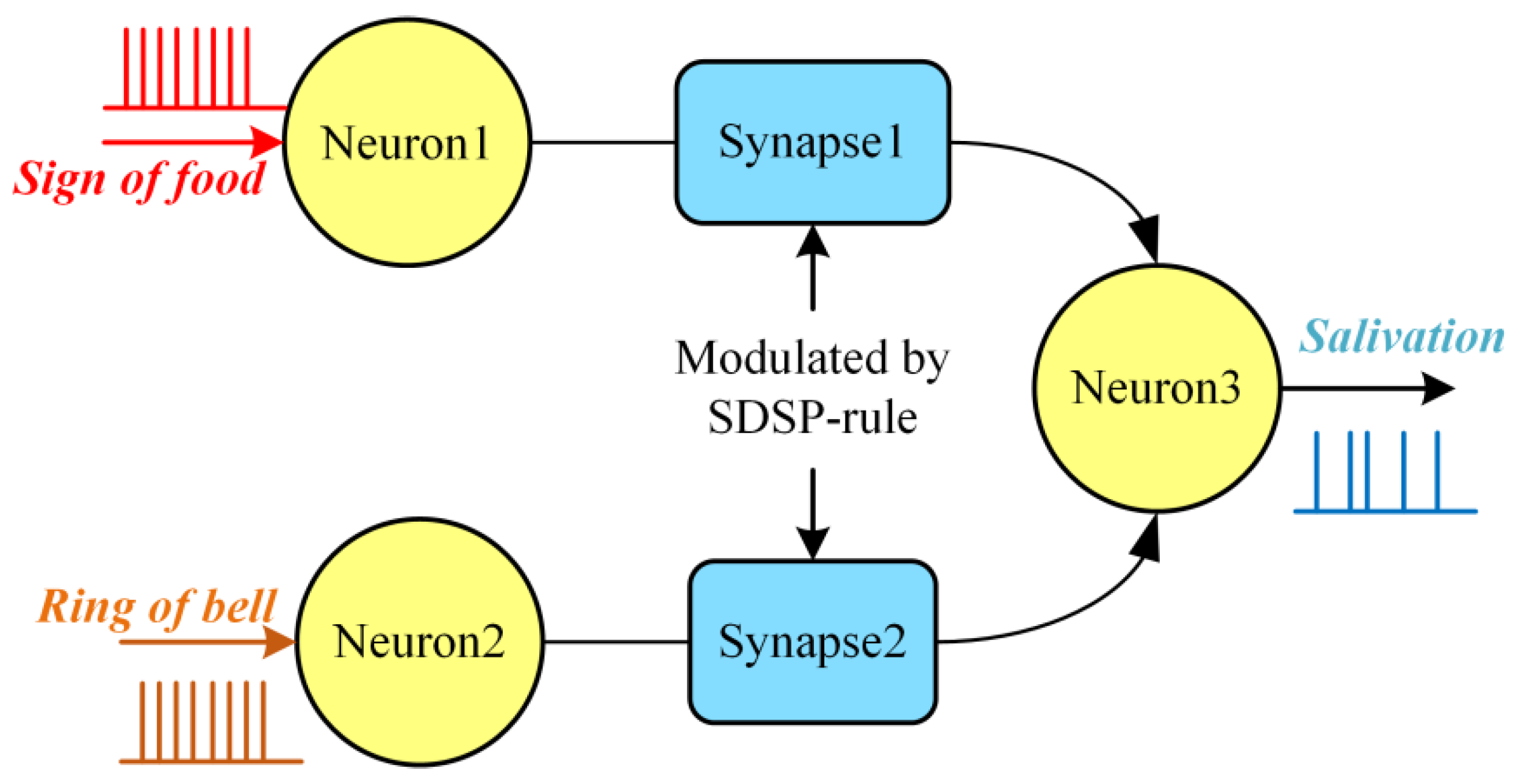
2. Mixed-Signal Pavlov SNN Circuit
2.1. SOI Process Advantages
- (a)
- Low Noise and Crosstalk: SOI CMOS enables novel process and design techniques to achieve a very low noise operation and lower crosstalk to support high-performance mixed-mode circuits.
- (b)
- Reduce Parasitic: Isolation from the lumped silicon substrate reduces the capacitive load, thus providing better performance and lower power consumption.
2.2. Key Circuit in 180 nm PDSOI Process
- (1)
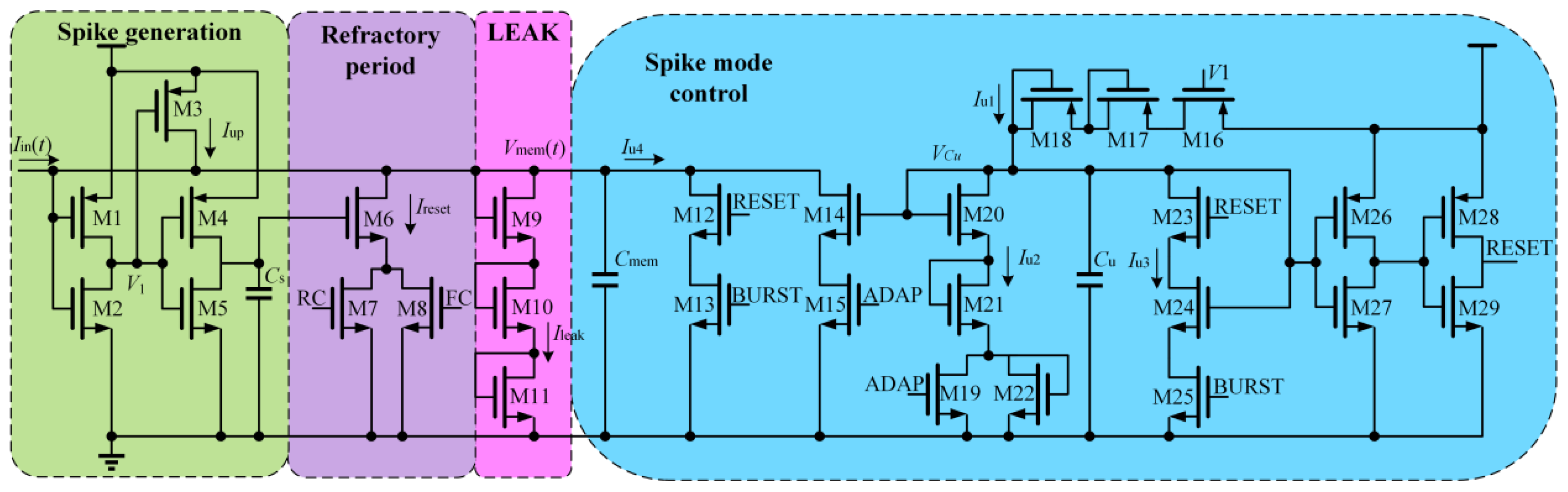
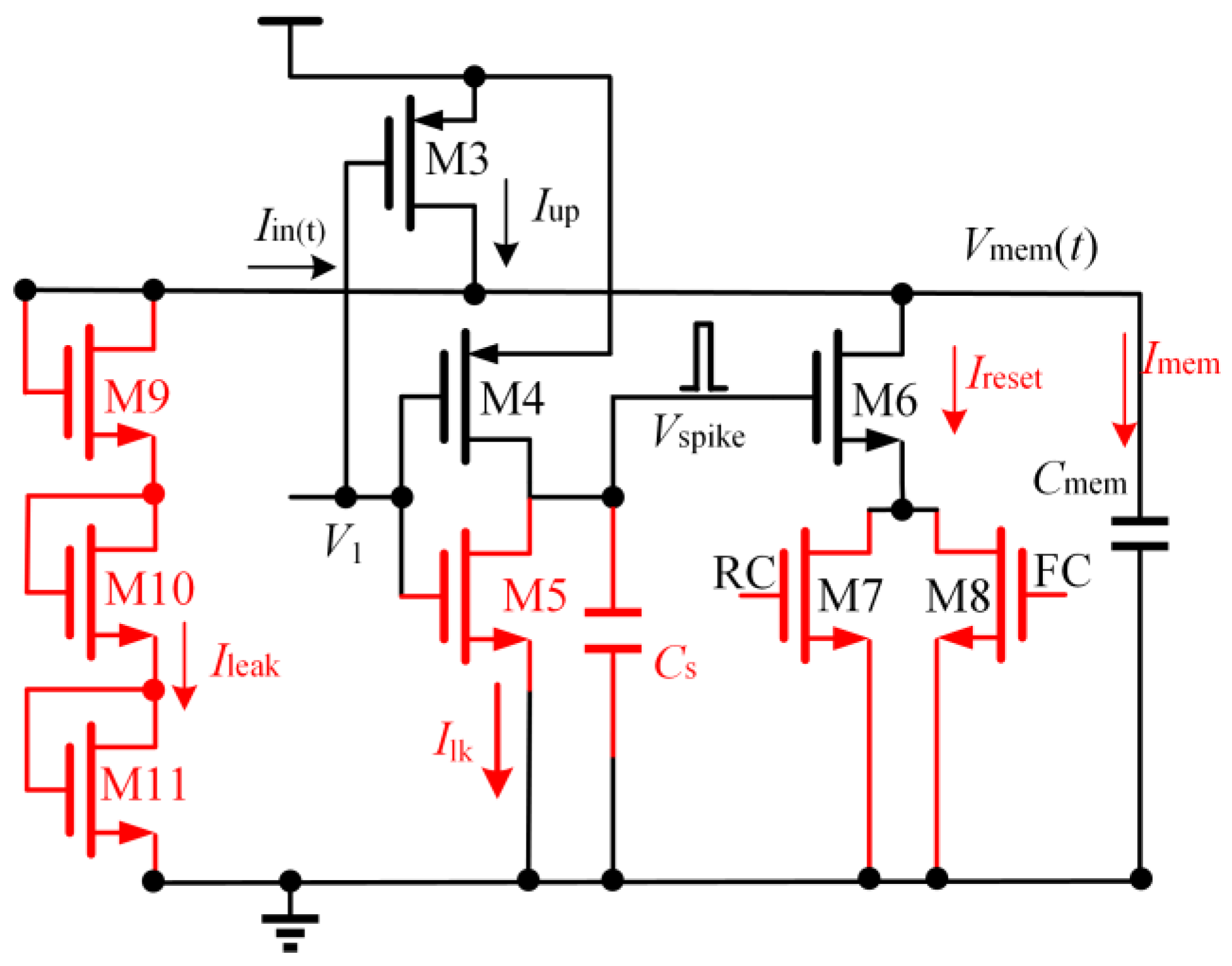
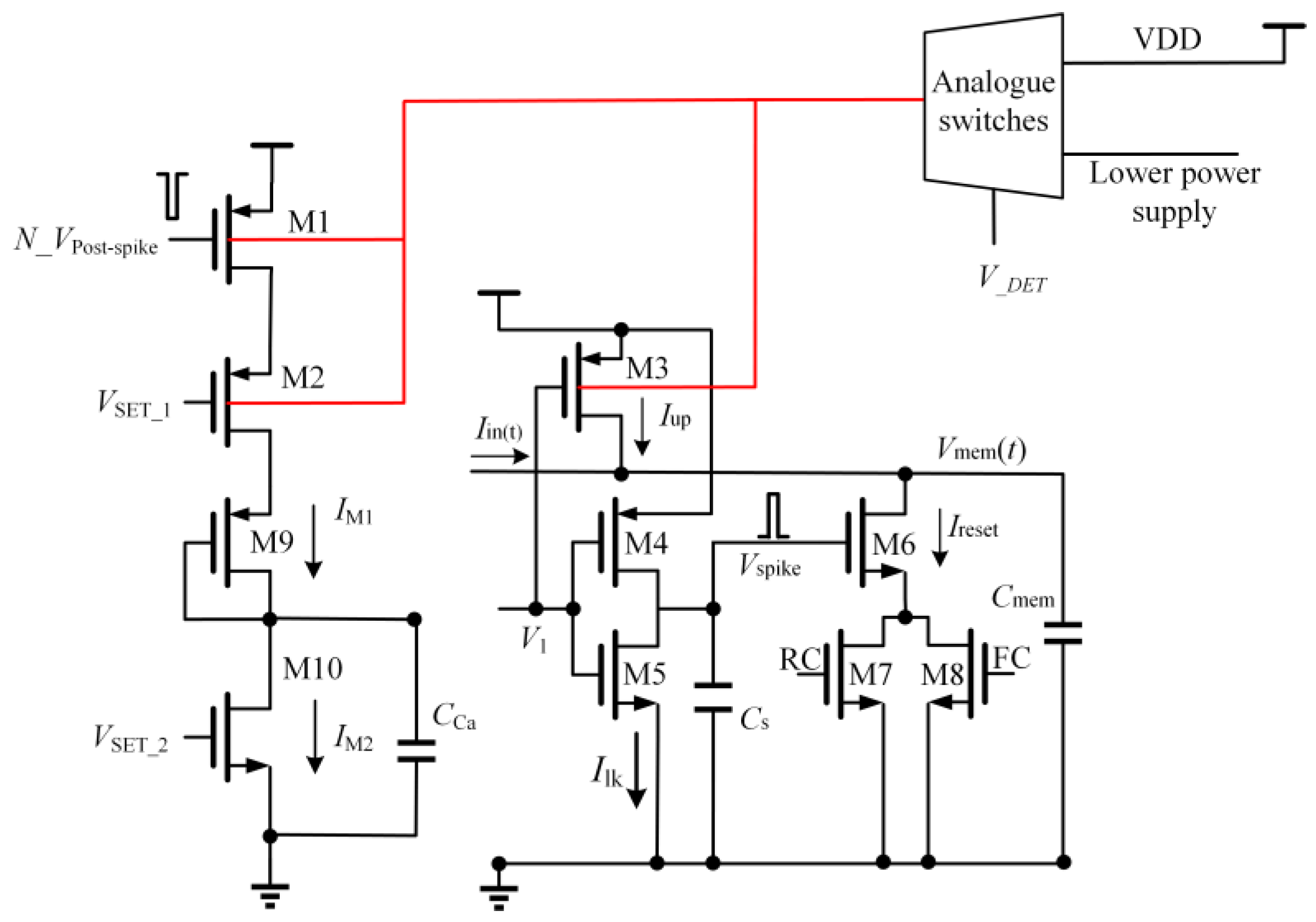
- Mixed-Signal Spike Neuron Circuit
- (2)
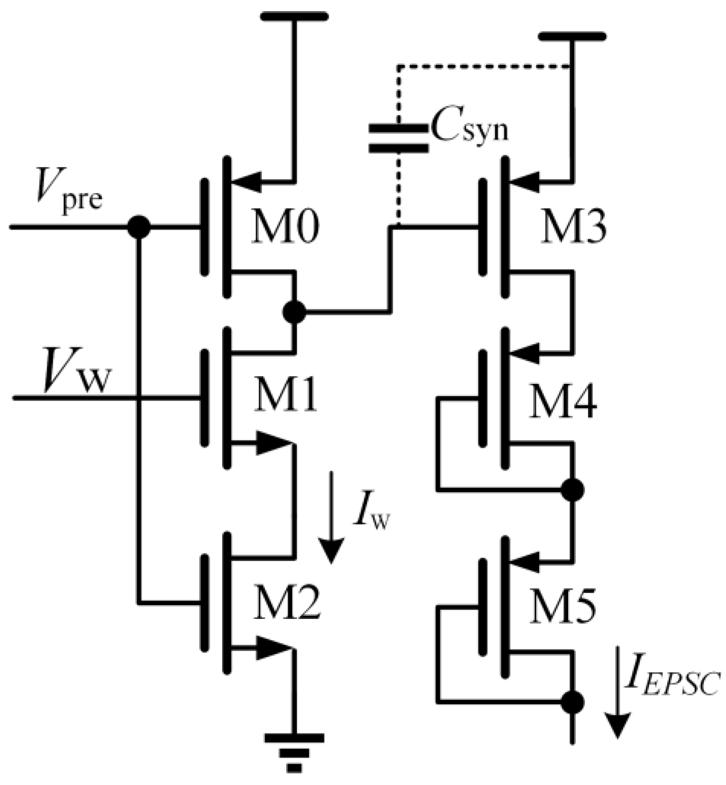
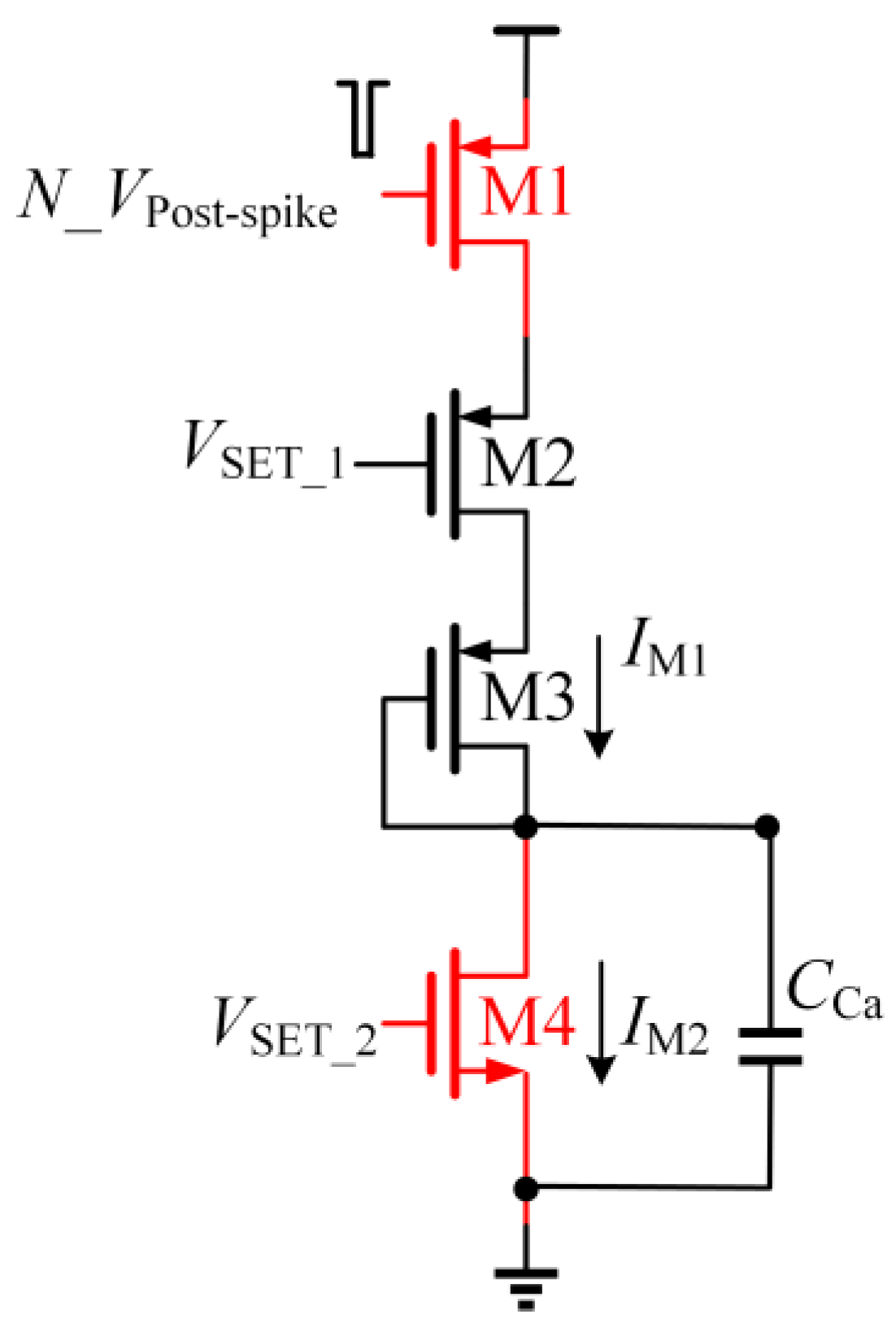
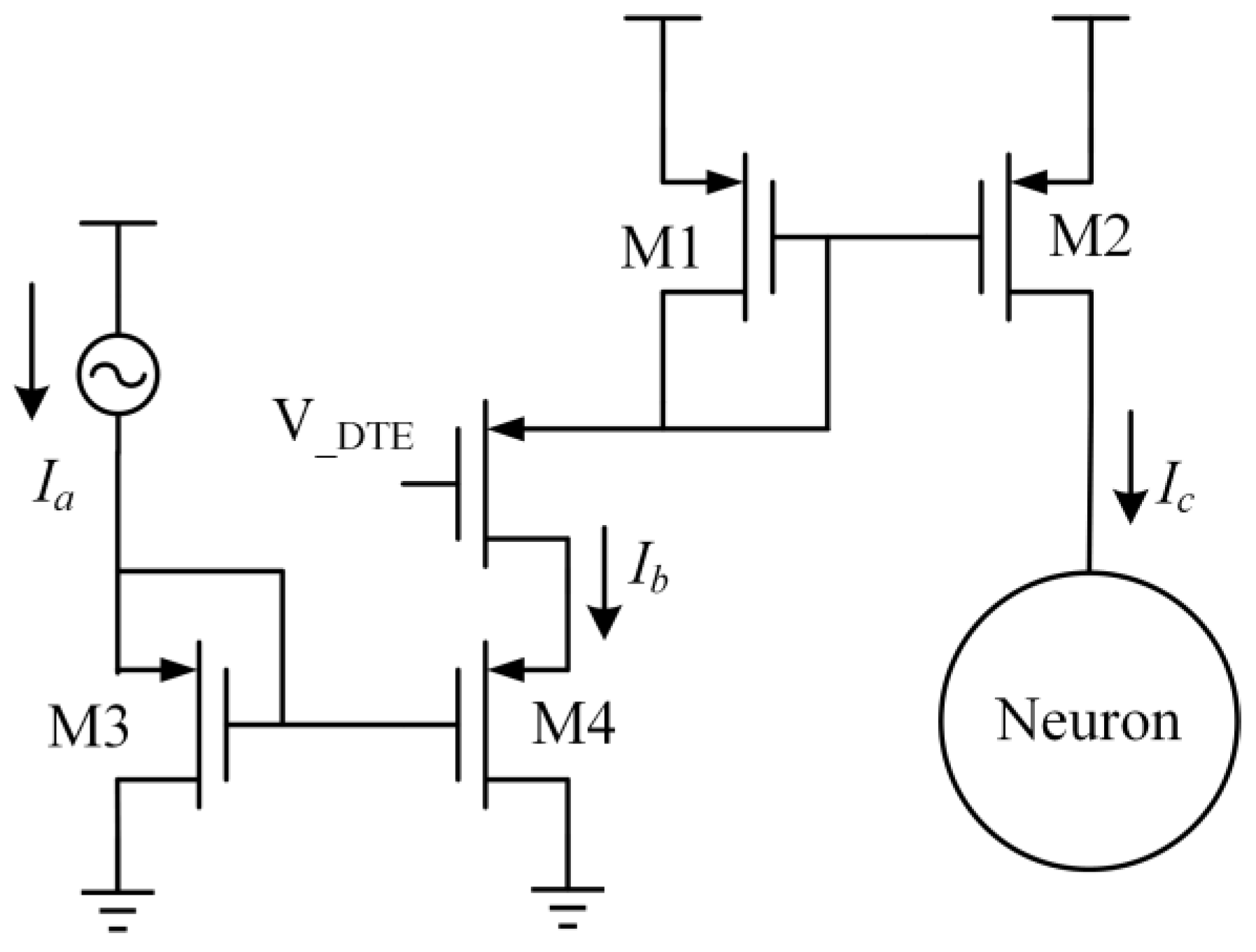
- Synapse Circuit
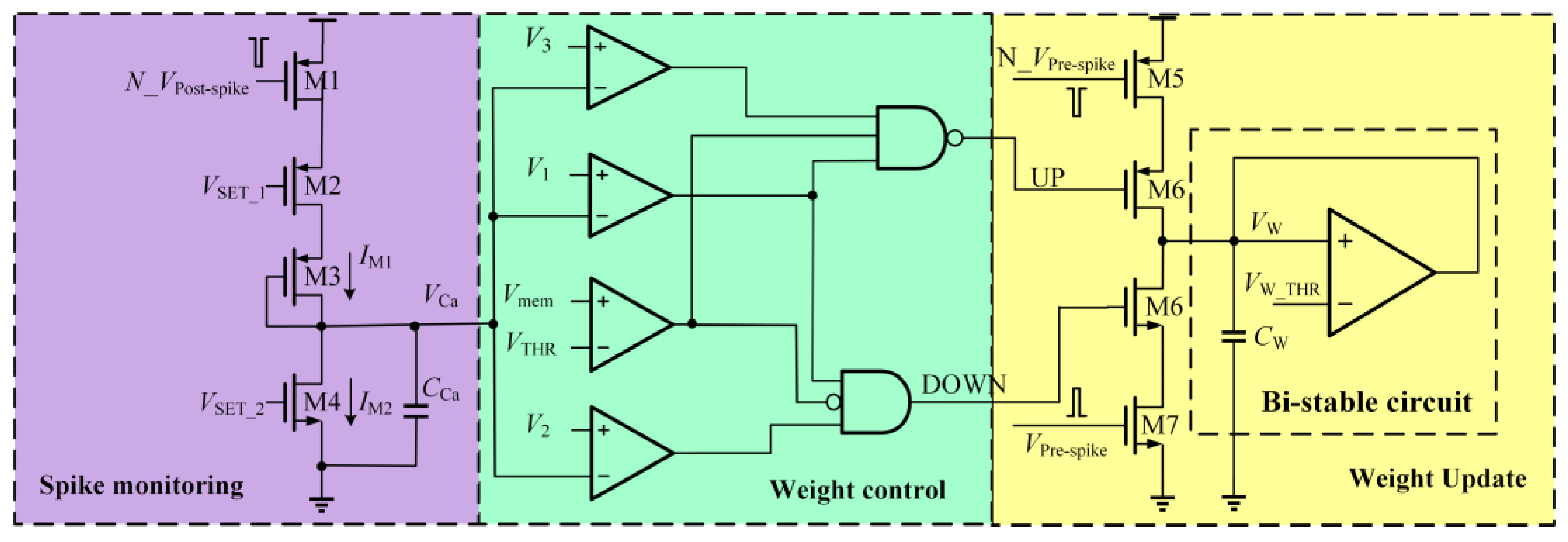
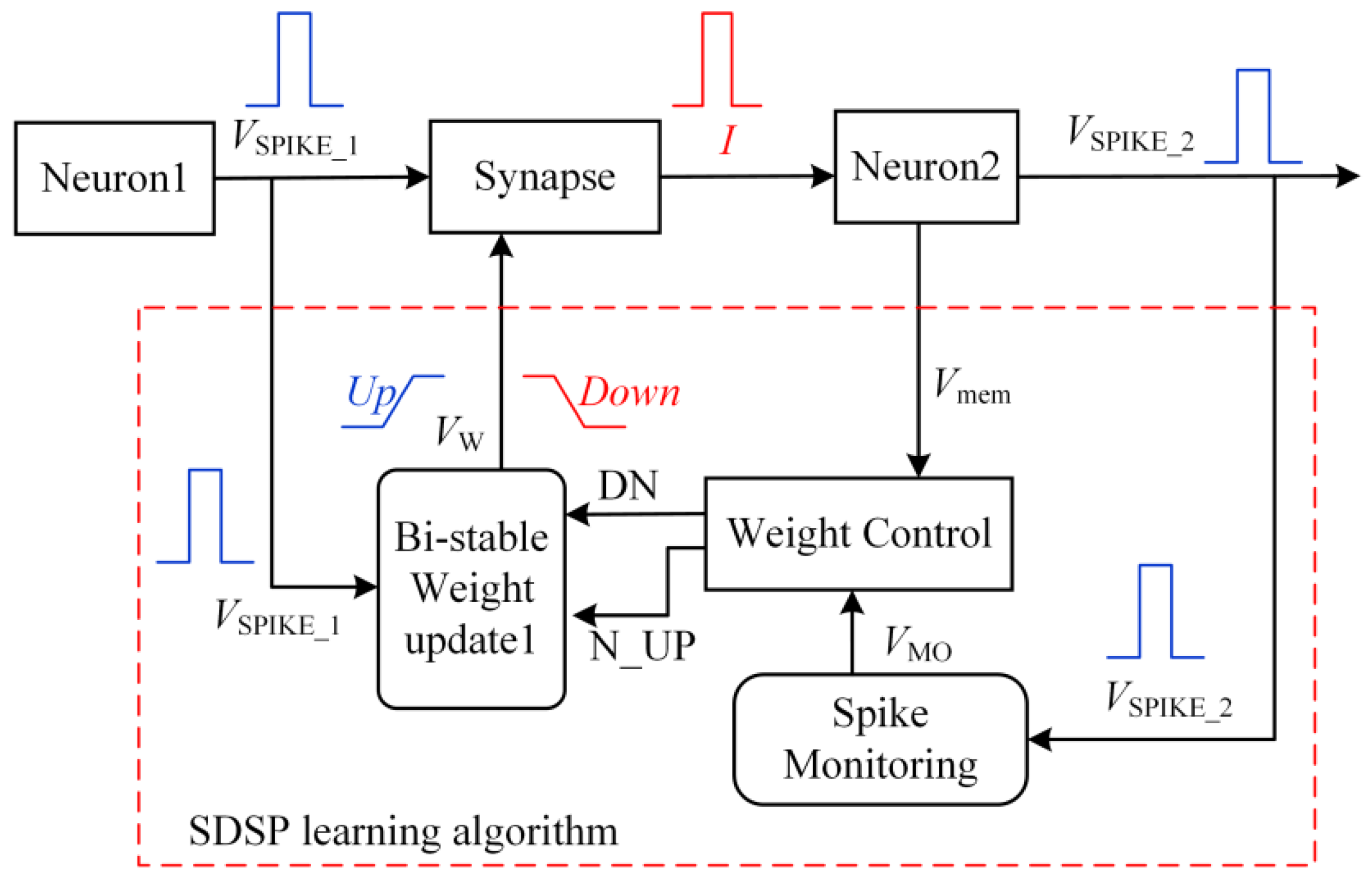
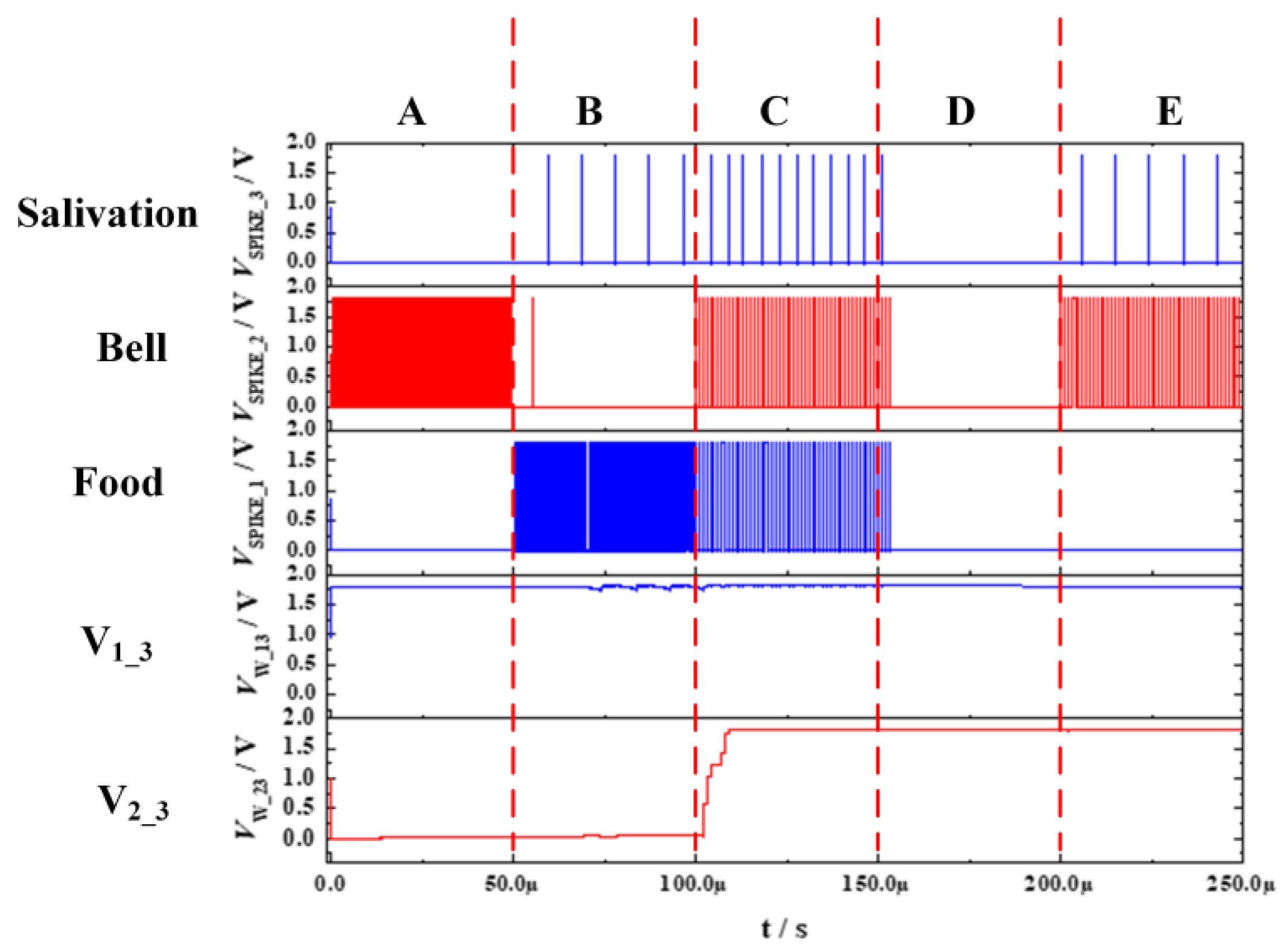
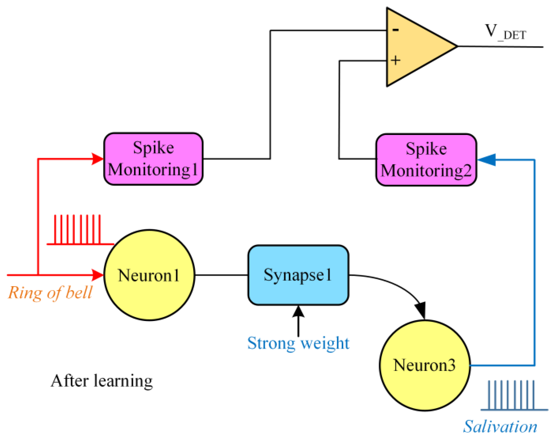
2.3. Mixed-Signal Pavlov SNN
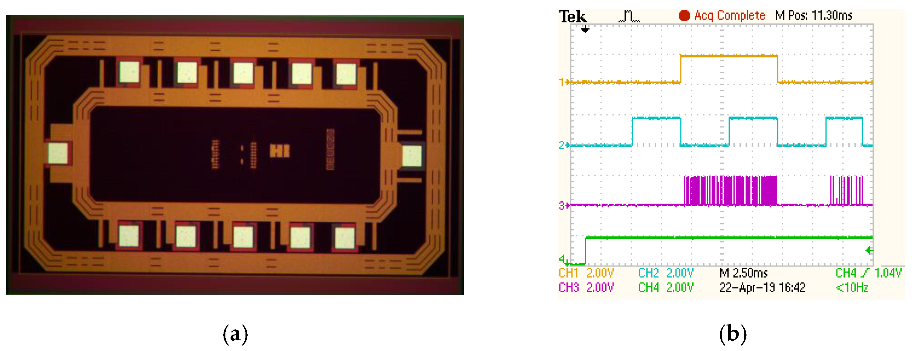
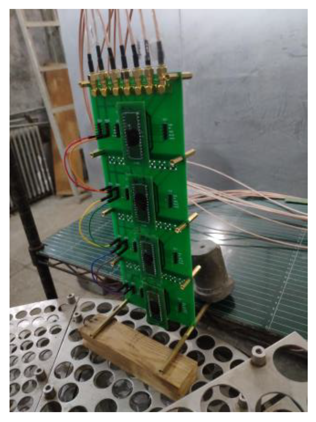
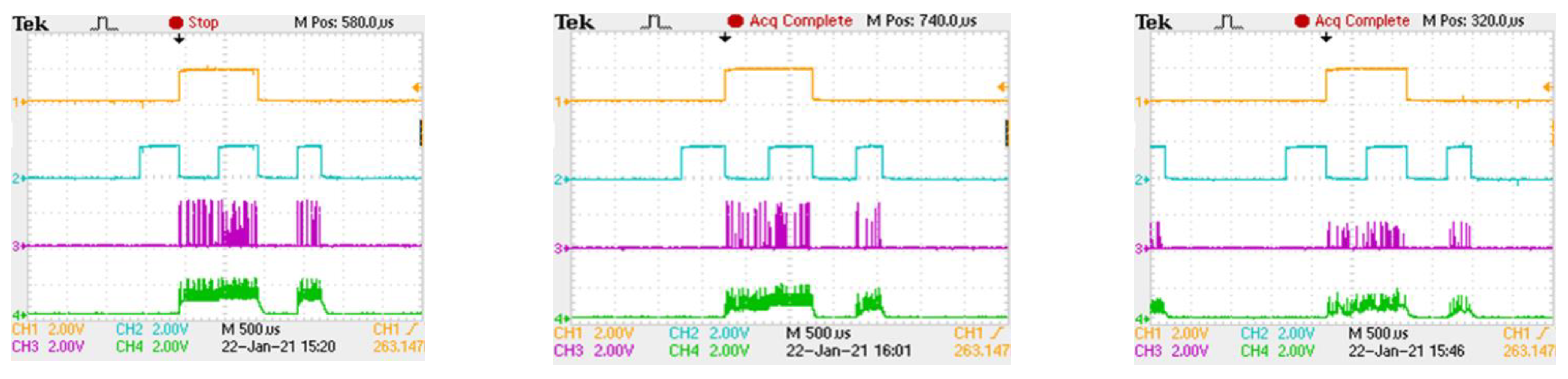
2.4. Prototype and Test
3. Experimental Results and Discussion of Radiation-Hardening Techniques
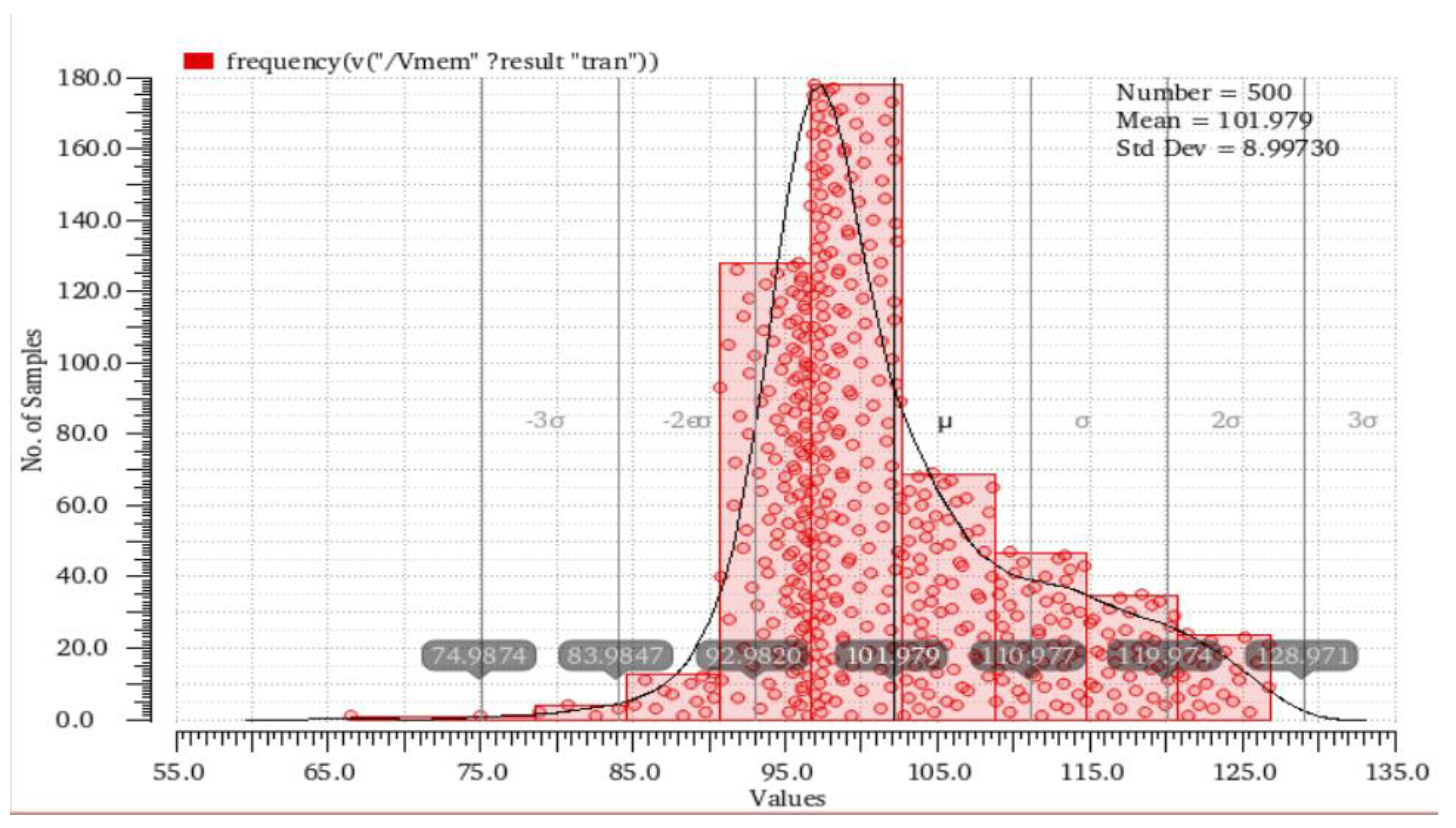
3.1. Experimental Results
3.2. Discussion of Radiation-Hardening Techniques
4. Conclusions
Author Contributions
Funding
Data Availability Statement
Conflicts of Interest
References
- Merolla, P.A.; Arthur, J.V.; Alvarez-Icaza, R.; Cassidy, A.S.; Sawada, J.; Akopyan, F.; Jackson, B.L.; Imam, N.; Guo, C.; Nakamura, Y.; et al. A million spiking-neuron integrated circuit with a scalable communication network and interface. Science 2014, 345, 668–673. [Google Scholar] [CrossRef] [PubMed]
- Mead, C. Neuromorphic electronic systems. Proc. IEEE 1990, 78, 1629–1636. [Google Scholar] [CrossRef] [Green Version]
- Shi, L.; Pei, J.; Deng, N.; Wang, D.; Deng, L.; Wang, Y.; Zhang, Y.; Chen, F.; Zhao, M.; Song, S.; et al. Development of a neuromorphic computing system. In Proceedings of the 2015 IEEE International Electron Devices Meeting (IEDM), Washington, DC, USA, 7–9 December 2016. [Google Scholar]
- Qiao, N.; Mostafa, H.; Corradi, F.; Osswald, M.; Stefanini, F.; Sumislawska, D.; Indiveri, G. A reconfigurable on-line learning spiking neuromorphic processor comprising 256 neurons and 128 K synapses. Front. Neurosci. 2015, 29, 141. [Google Scholar]
- Zhang, P.; Cao, Y.; Li, S. Analysis of the Application Prospect of Artificial Intelligence in Space. In Proceedings of the 2019 IEEE 3rd Advanced Information Management, Communicates, Electronic and Automation Control Conference (IMCEC), Chongqing, China, 11–13 October 2019; pp. 1238–1241. [Google Scholar]
- Ye, Z.; Liu, R.; Taggart, J.L.; Barnaby, H.J.; Yu, S. Evaluation of radiation effects in RRAM-based neuromorphic computing system for inference. IEEE Trans. Nucl. Sci. 2018, 66, 97–103. [Google Scholar] [CrossRef]
- Izhikevich, E.M. Simple model of spiking neurons. IEEE Trans. Neural Netw. 2003, 14, 1569–1572. [Google Scholar] [CrossRef] [PubMed] [Green Version]
- Wijekoon, J.H.; Dudek, P. Compact silicon neuron circuit with spiking and bursting behaviour. Neural Netw. 2008, 21, 524–534. [Google Scholar] [CrossRef]
- Qiao, N.; Indiveri, G. Scaling mixed-signal neuromorphic processors to 28 nm FD-SOI technologies. In Proceedings of the 2016 IEEE Biomedical Circuits and Systems Conference (BioCAS), Shanghai, China, 11–17 October 2016; pp. 552–555. [Google Scholar]
- Akbari, M.; Hussein, S.M.; Chou, T.I.; Tang, K.T. A 0.3-V Conductance-Based Silicon Neuron in 0.18 μm CMOS Process. IEEE Trans. Circ. Syst. II Express Briefs 2021, 68, 3209–3213. [Google Scholar] [CrossRef]


Publisher’s Note: MDPI stays neutral with regard to jurisdictional claims in published maps and institutional affiliations. |
© 2022 by the authors. Licensee MDPI, Basel, Switzerland. This article is an open access article distributed under the terms and conditions of the Creative Commons Attribution (CC BY) license (https://creativecommons.org/licenses/by/4.0/).
Share and Cite
Liu, Z.; Li, B.; Quan, J.; Luo, J. Total-Ionization-Dose Radiation Effects and Hardening Techniques of a Mixed-Signal Spike Neural Network in 180 nm SOI-Pavlov Process. Electronics 2022, 11, 1643. https://0-doi-org.brum.beds.ac.uk/10.3390/electronics11101643
Liu Z, Li B, Quan J, Luo J. Total-Ionization-Dose Radiation Effects and Hardening Techniques of a Mixed-Signal Spike Neural Network in 180 nm SOI-Pavlov Process. Electronics. 2022; 11(10):1643. https://0-doi-org.brum.beds.ac.uk/10.3390/electronics11101643
Chicago/Turabian StyleLiu, Zhen, Bo Li, Jiale Quan, and Jiajun Luo. 2022. "Total-Ionization-Dose Radiation Effects and Hardening Techniques of a Mixed-Signal Spike Neural Network in 180 nm SOI-Pavlov Process" Electronics 11, no. 10: 1643. https://0-doi-org.brum.beds.ac.uk/10.3390/electronics11101643