
Designs of Level-Sensitive T Flip-Flops and Polar Encoders Based on Two XOR/XNOR Gates


1
School of Computer Science and Technology, Anhui University, Hefei 230601, China
2
School of Microelectronic, Hefei University of Technology, Hefei 230009, China
3
Laboratory of Informatics, Robotics and Microelectronics of Montpellier, University of Montpellier, CNRS, 34095 Montpellier, France
4
Graduate School of Computer Science and Systems Engineering, Kyushu Institute of Technology, Fukuoka 820-8502, Japan
*
Author to whom correspondence should be addressed.
Electronics 2022, 11(10), 1658; https://0-doi-org.brum.beds.ac.uk/10.3390/electronics11101658
Submission received: 5 April 2022
/
Revised: 8 May 2022
/
Accepted: 11 May 2022
/
Published: 23 May 2022
(This article belongs to the Section Quantum Electronics)
Abstract
:Quantum-dot cellular automata is a novel nanotechnology that has the advantages of low energy dissipation, easy integration, and high computing speed. It is regarded as one of the powerful alternative technologies for the next generation of integrated circuits because of its unique implementation concept. In this paper, two XOR/XNOR gates are proposed. Level-sensitive T flip-flops, negative edge-trigger T flip-flops, two-to-one multiplexers, reversible gates, and (8, 4) polar encoders are implemented based on these two proposed logic gates. Simulation results show that, compared with the existing level-sensitive T flip-flops, the second proposed level-sensitive T flip-flop has fewer cells and lower energy dissipation; compared with the best (8, 4) polar encoder, the cell count and area of the second proposed (8, 4) polar encoder are decreased by 13.67% and 12.05%, respectively. The two XOR/XNOR gates have a stable output and low energy dissipation, which can be flexibly designed into complex quantum-dot cellular automata circuits.
1. Introduction
The exponential shrinking of transistor feature sizes causes severe challenges for energy dissipation and the manufacturing of CMOS technologies [1]. Quantum-dot Cellular Automata (QCA) is considered to be a feasible alternative scheme that promises quick operations with low energy dissipation at a high frequency. The favorable characteristics of QCA make it possible to break through the bottleneck of traditional circuits and implement more efficient circuit performance.
The XOR gate is a typical logic gate in QCA circuits. In 2015, Chabi et al. proposed a novel XOR gate [2]. This design obtained the desired output based on the explicit Coulomb attraction between QCA cells, instead of the combinatorial logic expressions. The structure of the XOR gate is more concise because no other logic expressions are introduced. Later, many XOR/XNOR gates based on this design concept were proposed. A novel XOR/XNOR gate was proposed by Berarzadeh et al. [3], but the design has the disadvantage of a large area. Ahmad et al. proposed a novel three-input XOR gate [4]. The input and output can be easily accessed but it has the disadvantage of high energy dissipation. Chen et al. proposed a novel XOR gate in [5], made up of nine cells. In 2020, a new XOR/XNOR gate was proposed in [6], requiring two enable inputs. The design proposed by Laajimi et al. has the advantage of small area but its energy dissipation is high [7]. Majeed et al. [8] proposed a new XOR/XNOR gate and Safaiezadeh et al. [9] implemented a three-input XOR/XNOR gate, both of them having the disadvantage of high energy dissipation.
T flip-flop is an important sequential circuit. Vetteth et al. proposed a new QCA-based T flip-flop in [10] but with many QCA cells and thus a large area. Torabi et al. in [11] and Lim et al. in [12] proposed new T flip-flops, both of them having large areas. In 2014, a level-sensitive T flip-flop based on a new wiring approach was proposed by Angizi et al. [13]. In 2015, Angizi et al. proposed a new design of T flip-flops and used it to implement a three-bit synchronous counter [14]. Chakrabarty et al. proposed a T flip-flop by using a derived expression of so-called SR flip-flops [15], but the design has the disadvantages of large area and latency. Majeed et al. in [16] proposed a new level-sensitive T flip-flop by using the XOR in [5] and an AND gate.
Multiplexers have important applications in circuits. In 2008, Hashemi et al. proposed a two-to-one multiplexer but with a large circuit area [17]. In 2014, Sabbaghi-Nadooshan et al. proposed a two-to-one multiplexer but with a large cell count [18]. In 2017, Chabi et al. [19] proposed a two-to-one multiplexer using an XOR gate and a three-input majority gate. In 2018, Ahmad [20] proposed a two-to-one multiplexer using three three-input majority gates but with low fault tolerance. Reversible gates can be used in combinatorial logic circuits. There are many reversible gates such as the Feynman gate, Toffoli gate, Fredkin gate, and Peres Gate. In 2007, Ma et al. [21] designed a Fredin gate based on QCA. Ben et al. proposed new QCA-based reversible gates in [22,23]. In 2017, Chabi et al. proposed a new reversible gate in [19]. In 2021, Khosroshahy et al. proposed a novel reversible and fault-tolerant nano-communication parity-based arithmetic circuit [24]. In 2017, Khosroshahy et al. proposed an effective solution to reduce the number of external input cells providing fixed inputs, which simplifies the overall circuit implementation and fabrication [25]. In 2022, an ultra-high-speed fault-tolerant full-adder cell was proposed in [26], which has performance improvements in complexity, area consumption, delay, and total energy.
The QCA technology can also be used in the designs of encoder and decoder circuits. In 2018, Das et al. in [27] proposed an (8, 4) polar encoder based on XOR gates. The circuit used XOR gates based on the traditional and combinatorial logic expressions, resulting in many redundant cells. In 2020, Ahmed et al. in [28] proposed an (8, 4) polar encoder that has the disadvantages of large area and latency.
The above solutions mainly have the disadvantage that their overhead is large. To reduce the overhead of these circuits, new designs are proposed. The contributions of this paper are listed as follows:
- (1)
- Two XOR/XNOR gates based on the explicit interaction between cells are proposed. Both of them have a stable output and low energy dissipation.
- (2)
- Level-sensitive T flip-flops and negative edge-trigger T flip-flops are implemented. Compared with the existing designs, the second proposed level-sensitive T flip-flop has fewer cells and lower energy dissipation.
- (3)
- Two-to-one multiplexers are implemented and the reversible gate in [19] is improved based on three XOR gates, respectively. The designed reversible gates have the characteristics of small cell count and small area.
- (4)
- Two (8, 4) polar encoders based on the proposed XOR gates are implemented. Compared with the best design, both of the proposed (8, 4) polar encoders have lower latency, fewer cells, and smaller areas.
- (5)
- The layouts of the proposed QCA circuits are designed in QCA Designer [29]. The functions of the proposed designs are verified in QCA Designer, which proves the feasibility of the proposed designs. The total and average energy dissipation are estimated by QCA Designer-E [30]. The existing alternatives and the proposed designs are analyzed and evaluated.
The rest of this paper is organized as follows. Section 2 gives some preliminaries about QCA and introduces existing XOR gates and two proposed XOR/XNOR gates. Section 3 mainly presents the QCA circuits based on two proposed XOR/XNOR gates, including level-sensitive T flip-flops, negative edge-trigger T flip-flops, two-to-one multiplexers, reversible gates, and (8, 4) pole encoders. Section 4 concludes this paper.
2. Proposed XOR/XNOR Gates and Comparisons
2.1. Preliminaries
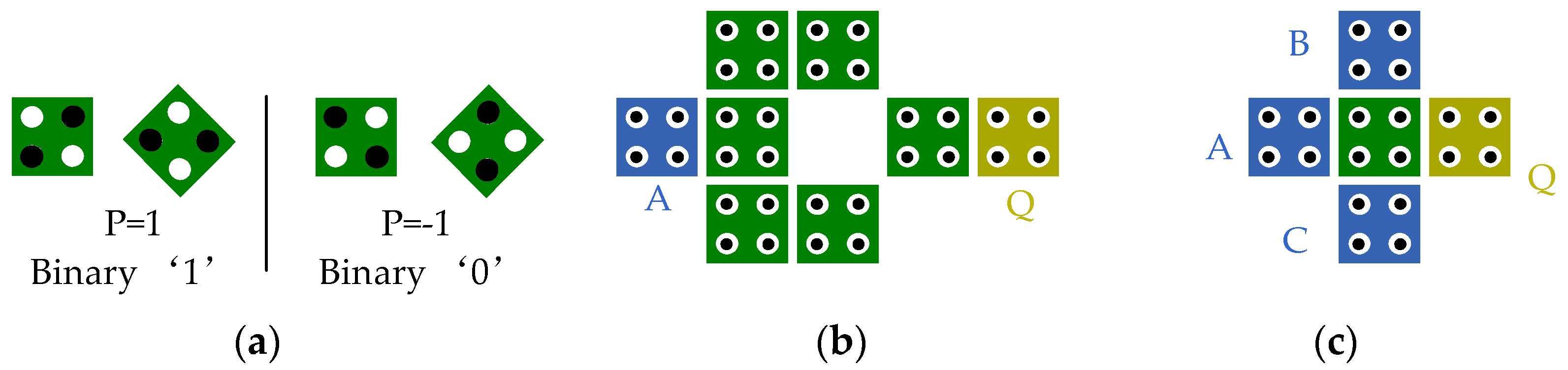
A QCA cell is the most basic component unit of QCA. There are four quantum dots and two free electrons in a QCA cell. Two free electrons can move freely among the four quantum dots in a QCA cell and can reach two stable states due to electrostatic interaction. The two stable states can represent the binary ‘1’ and binary ‘0’. Figure 1 shows the basic units in the QCA technology. QCA cells can be divided into normal cells and rotated cells. Figure 1a shows the two stable states of QCA cells. Figure 1b shows an inverter and Figure 1c shows a three-input majority gate. The inverter can reverse an input signal and the three-input majority gate can output a signal that follows the majority rule. So far, to the best of our knowledge, there are four different models of QCA (including metal island, semiconductor, magnetic, and molecular). There are many theories for each of the four schemes. Molecular QCA cells and magnetic QCA cells can work stably at room temperature.
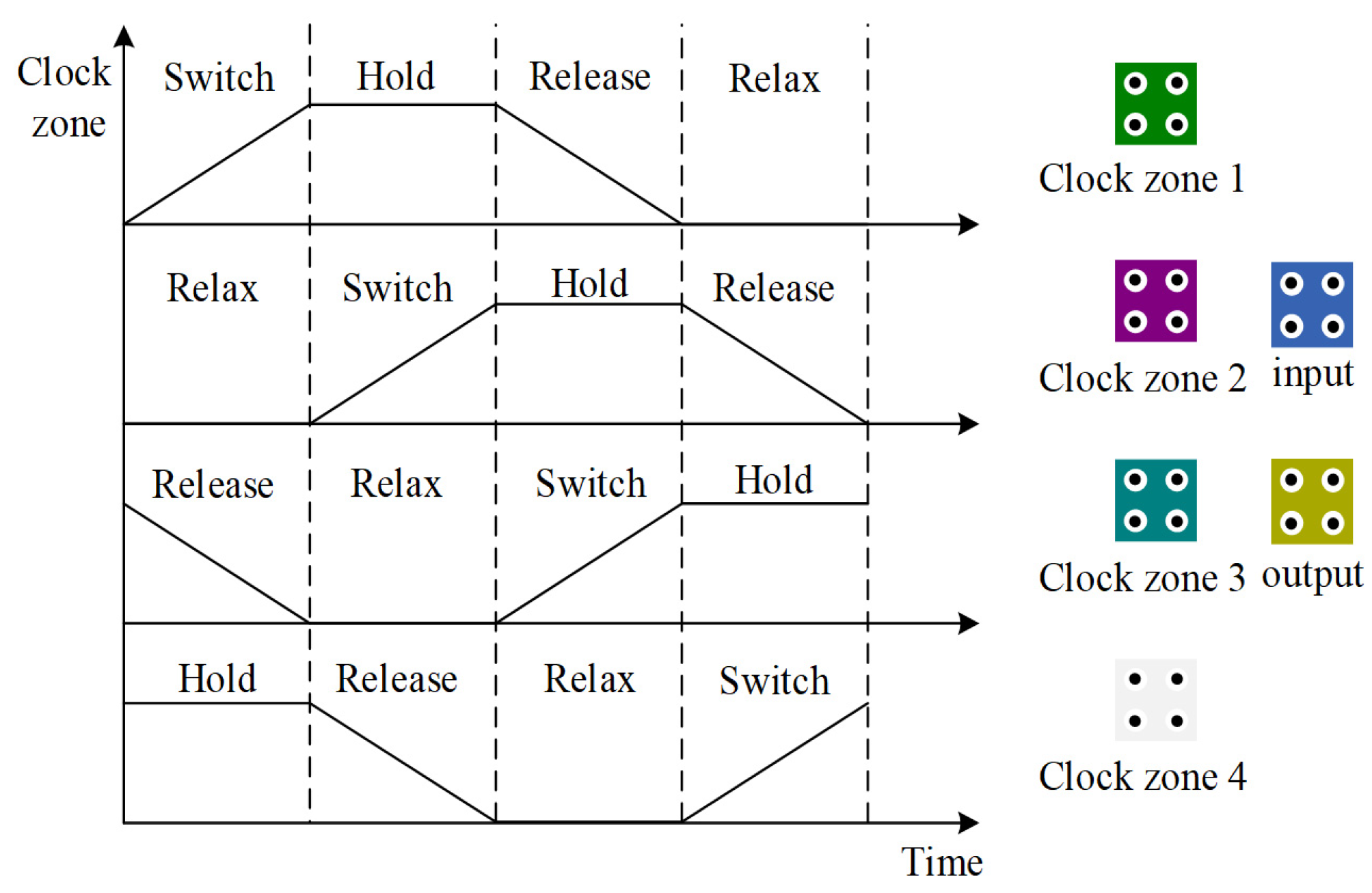
A QCA circuit is separated by different clock zones so that all QCA cells in each zone are controlled by the same clock signal and perform specific operations. Figure 2 shows the QCA clock. Switch, hold, release, and relax are four clock phases in a clock. In the switch phase, the cell enters a polarized state according to the state of the drive cell. In the hold stage, the maximum polarity of cells remained unchanged. During the release phase, the cell begins to lose polarity. In the relax phase, the cell is in a non-polarized state. These clocks are 90 degrees out of phase so as to ensure the correct transmission of signals. The cells of the four clocks are represented by four different colors. The blue cell is the input cell and the yellow cell is the output cell.
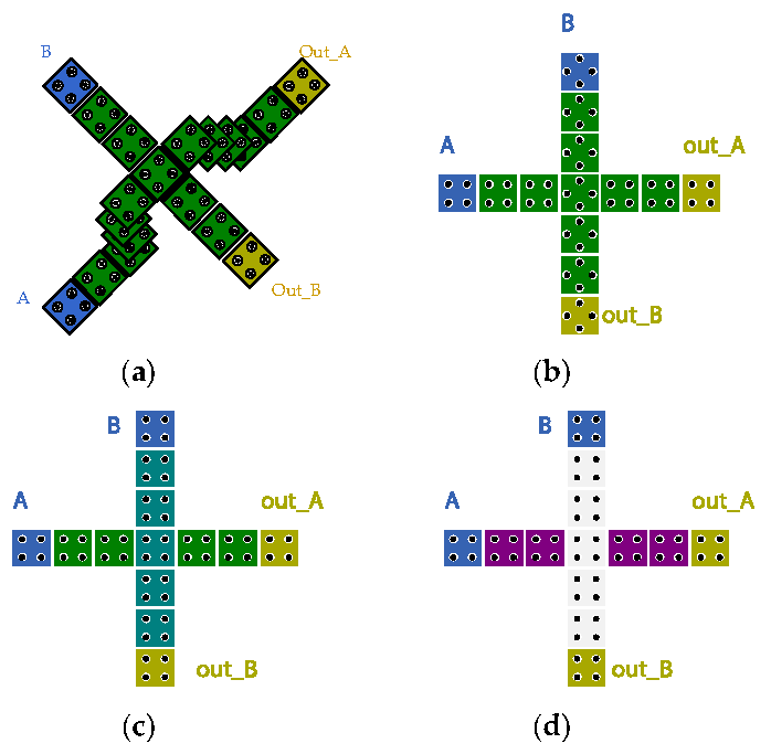
Figure 3 shows several different crosswires. Multi-layer crosswire uses the way of multi-layer wiring to implement the cross-transmission of signals. The disadvantage is that it is difficult to manufacture. Coplanar crosswires can be implemented by rotated QCA cells and normal QCA cells. When rotated QCA cells and normal QCA cells transmit signals, the Coulomb force between cells does not interfere with neighboring cells because the electron configuration of the two cells is orthogonal [31]. Because crosswires using rotated cells are irregular, Shin et al. proposed a new coplanar crosswire using different clock zones (using clock zones 1 and 3 or clock zones 2 and 4) [32]. Cells in the switch phase can cross cells in the release phase and cells in the hold phase can cross cells in the relax phase. Signals can be transmitted normally because of no interaction between cells. In 2013, Bhanja proposed robust coplanar crosswires to enhance the fault tolerance of crosswires [33]. In 2016, Khosroshahy et al. proposed a new crosswire based on a new approach. The method can be used to design three-dimensional (3D) two-layer devices with a 1/0 logic value [34].
2.2. The Existing XOR/XNOR Gates
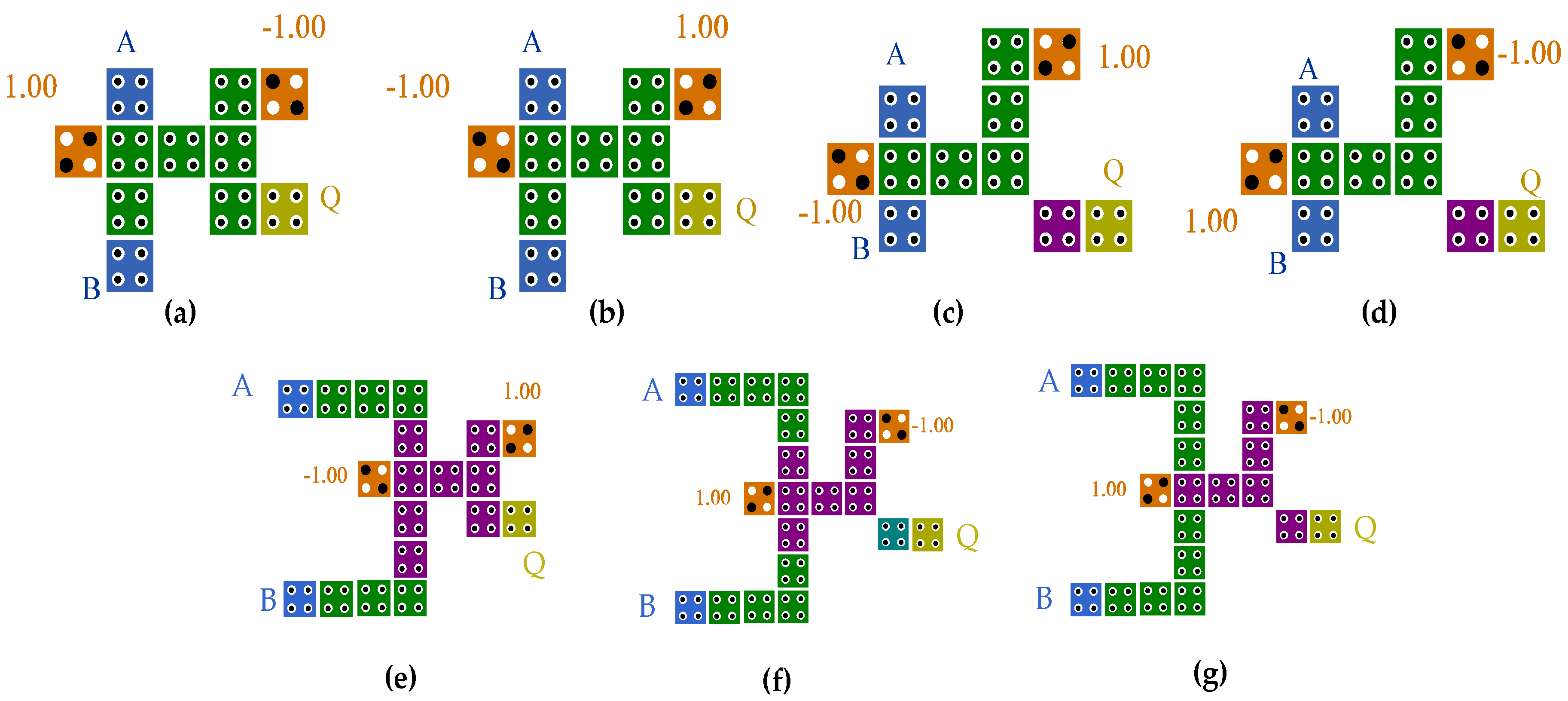
Figure 4 shows the existing XOR/XNOR gates, which are based on explicit Coulomb force to obtain the correct output. Figure 4a,b,d–g are two-input XOR gates, and Figure 4c,h are three-input XOR gates. By setting one of the input terminals of the three-input XOR gates to ‘−1’, the function of the two-input XOR gates can be implemented.
The advantages and disadvantages of alternative XOR/XNOR gates are given in Table 1. The design proposed by Chen et al. (see Figure 4d) is an efficient XOR gate with a smaller number of cells and lower power consumption among existing schemes. It is only implemented by nine cells with a delay of 0.25 clock cycles. However, due to the small number of cells, the fault-tolerant performance of the gate decreases, which should be paid attention to in practical applications. Figure 4c is an XOR gate based on the five-input majority gate. The layouts in Figure 4f–h are more compact and they are all based on a 3 × 3 module. The three gates have the disadvantage of high energy consumption.
2.3. Proposed XOR/XNOR Gates
In this section, two XOR/XNOR gates are proposed. Two proposed gates are based on [3,5], respectively. There are similarities in structure. Both of them are based on the explicit Coulomb force between QCA cells to obtain correct outputs.
The following is a brief introduction to the operation principle of the gate circuit. QCA circuits rely on Coulomb force between electrons in quantum dots to transmit information. Due to the action of Coulomb force between cells, each cell has two stable states. The electrostatic energy of the whole circuit can be obtained by calculating the sum of the electrostatic energy of the driving cells to the electrons in the output cell. The final circuit output can be obtained by comparing the electrostatic energy of the circuit in different states. The rule is, ‘The lower the electrostatic energy of the QCA circuits is, the more stable it is. The final output results tend to the state of the circuit with low electrostatic energy.’ Formulae (1) and (2) are used to calculate the electrostatic energy between electrons. r is the distance between electrons.
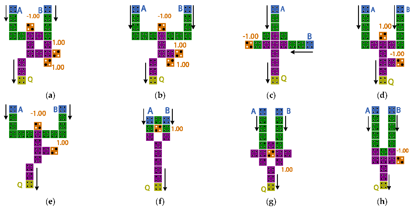
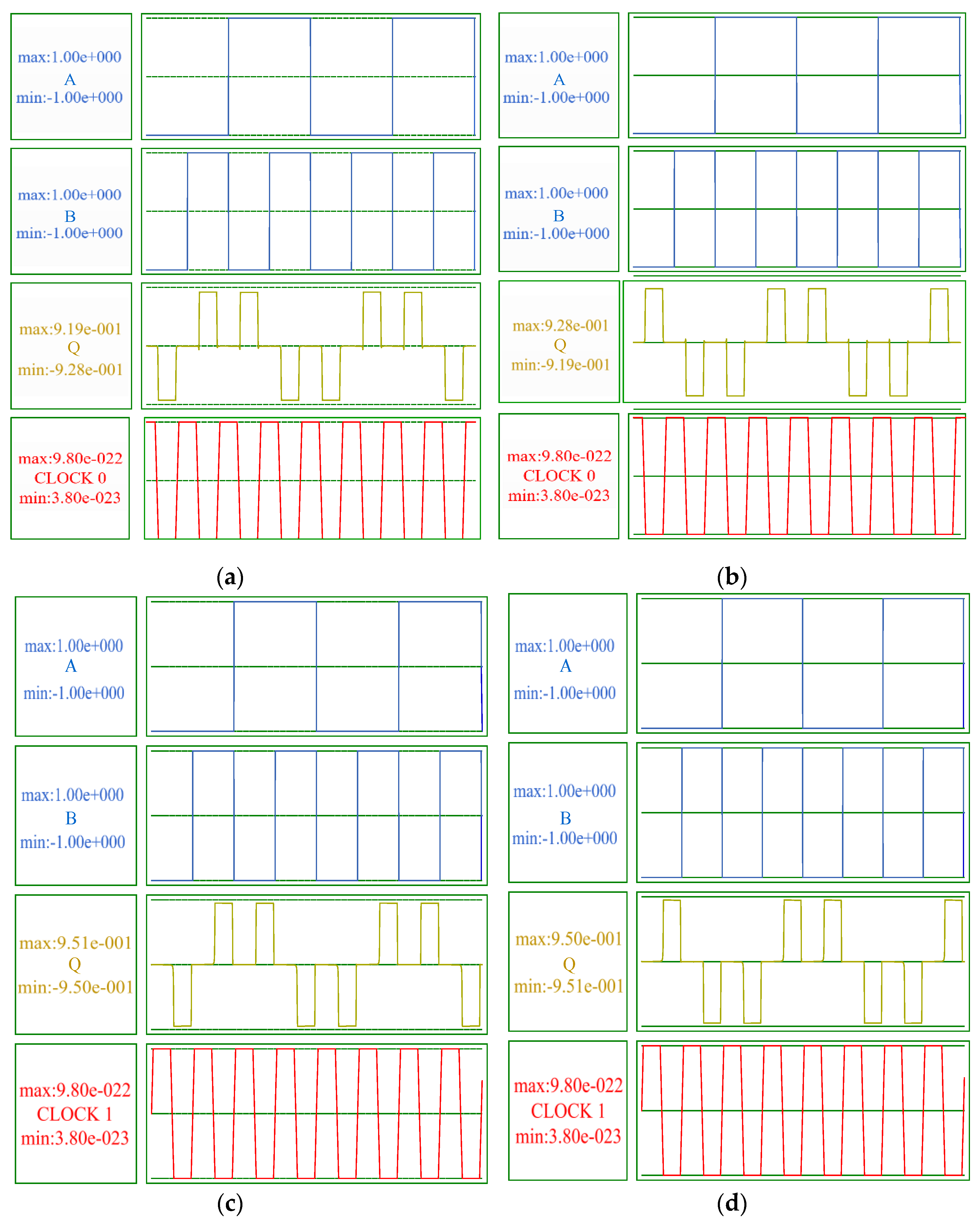
Figure 5 shows the proposed XOR/XNOR gates (XOR1, XNOR1, XOR2, and XNOR2) and Figure 6 shows the simulation results of two designs using the QCA Designer [29]. The parameters in QCA Designer are default and the simulation engine is Coherence Vector. Table 2 shows the default parameters for the coherence vector simulation engine in QCA Designer. As shown in Figure 5a,b, the proposed XOR1/XNOR1 gate consists of 11 QCA cells with an area of 7644 nm2 and a latency of 0.25 clock cycles. When the two enable inputs are set to (1, −1), the XOR operation is performed. Similarly, when the two enable inputs are set to (−1, 1), the XNOR operation is performed. As shown in Figure 5c,d, the proposed XOR2/XNOR2 gate consists of 11 QCA cells with an area of 9204 nm2 and a latency of 0.50 clock cycles. When the two enable inputs are set to (−1, 1), the XOR operation is performed. When the two enable inputs are set to (1, −1), the XNOR operation is performed. Figure 5e shows the I/O access method for the first design. Figure 5f,g shows the two I/O access methods for the second design.
The simulation results of two XOR gates are shown in Figure 6a,c. When the two inputs {A, B} are set to {0, 0}, the output Q is ‘0’; when the {A, B} are set to {0, 1}, the output Q is ‘1’; when the {A, B} are set to {1, 0}, the output Q is ‘1’; when the {A, B} are set to {1, 1}, the output Q is ‘0’. The simulation results of two XNOR gates are shown in Figure 6b,d. When the {A, B} are set to {0, 0}, the output Q is ‘1’; when the {A, B} are set to {0, 1}, the output Q is ‘0’; when the {A, B} are set to {1, 0}, the output Q is ‘0’; when the {A, B} are set to {1, 1}, the output Q is ‘1’. It can be seen from Figure 6 that the functioning of the XOR/XNOR gates is correct. The waveform value of the XOR1 gate is in the range of (−9.28 × 10⁻¹~9.19 × 10⁻¹), and the waveform value of the XNOR1 gate is in the range of (−9.19 × 10⁻¹~9.28 × 10⁻¹). The waveform value of the XOR2 gate is in the range of (−9. × 10−1~9. × 10−1), and the waveform value of the XNOR2 gate is in the range of (−9.51 × 10⁻¹~9.50 × 10⁻¹).
2.4. Comparisons
Table 3 shows the comparisons of the circuit performance and energy dissipation of the existing XOR/XNOR gates. The area was calculated through layouts, the latency was calculated by identifying the number of used clock cycles, and the total and average energy dissipation of these gates were estimated with the QCA Designer-E tool [30]. Note that the simulation parameters of the QCA Designer-E were set as default values.
It can be seen from Table 3 that the cell count and area of the proposed gate designs are larger than those of the designs in [7,9]. However, the total and average energy dissipation of the designs in [7,9] are larger than those of the proposed gate designs. It can be seen from Table 3 that the energy dissipation of the proposed gate designs is smaller than the designs in [2,3,4,6,7,8,9], and the proposed XOR2/XNOR2 gate even consumes a much smaller energy dissipation than the proposed XOR1/XNOR1 gate due to its layout, as shown in Figure 5. Therefore, the two proposed gates are competitive, especially in terms of energy dissipation. The two proposed gate structures can be used in large QCA circuits with low power.
3. Proposed QCA Circuits and Comparisons
The proposed XOR/XNOR gates can be applied to the design of large QCA circuits. This section uses the proposed XOR/XNOR gates to implement level-sensitive T flip-flops (LST-FFs), negative edge-trigger T flip-flops (NET-FFs), two-to-one multiplexers, reversible gates, and (8, 4) polar encoders, respectively.
3.1. Level-Sensitive T Flip-Flops and Negative Edge-Trigger T Flip-Flops
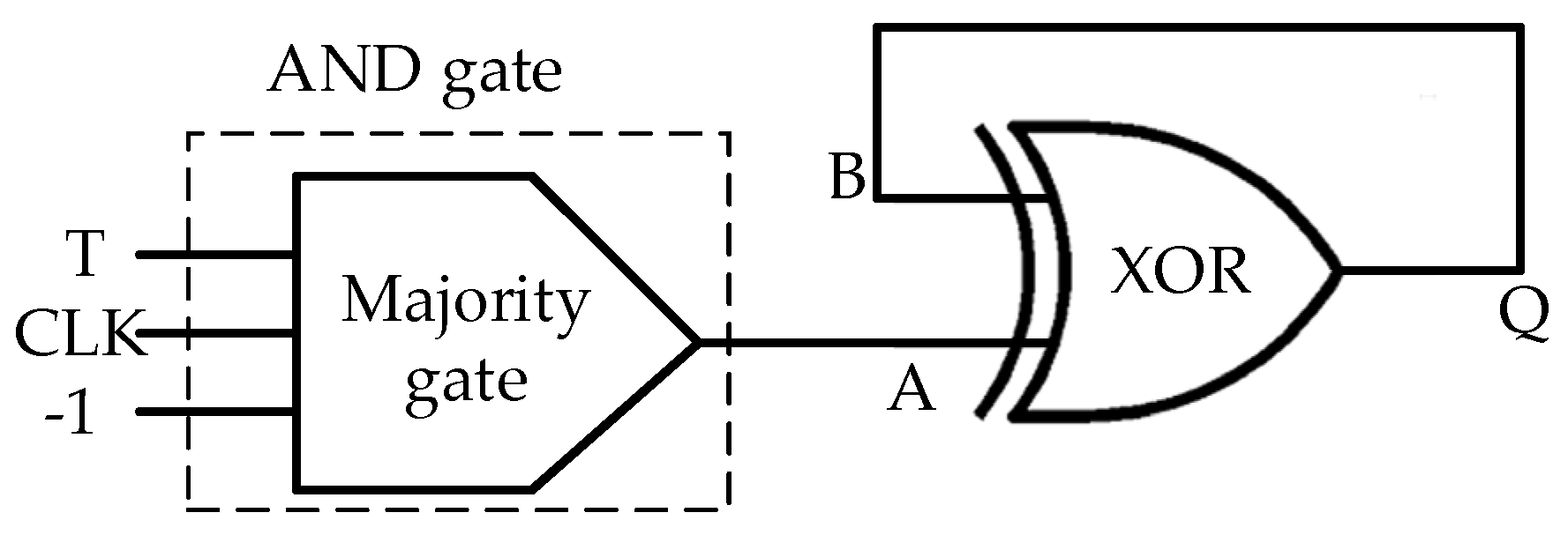
An LST-FF circuit can be implemented by using a two-input XOR gate with an AND gate [16]. Figure 7 shows the schematic diagram of the LST-FF. An AND gate in QCA can be implemented by setting one input of the three-input majority gate to ‘−1’. The signal CLK is the clock signal of the circuit. The signal T is the input signal.
The following explains how an LST-FF works. As shown in Figure 7, the result of the AND gate enters the input terminal A of the XOR gate, and a previous signal is fed back to an input terminal B of the XOR gate. When signals CLK and T are ‘0’, the AND gate outputs ‘0’, and the signal enters the XOR gate to perform the XOR operation. The current output signal of the LST-FF is the same as the previous output signal (i.e., CLK = 0, T = 0, ); when signal CLK is ‘0’ and signal T is ‘1’, the AND gate outputs ‘0’, and the signal enters the XOR gate to perform the XOR operation. The current output signal of the LST-FF is the same as the previous output signal (i.e., CLK = 0, T = 1, ); when signal CLK is ‘1’ and signal T is ‘0’, the AND gate outputs ‘0’, and the signal enters the XOR gate to perform the XOR operation. The current output signal of the LST-FF is the same as the previous output signal (i.e., CLK = 1, T = 0, ); when signals T and CLK are set to ‘1’, the AND gate outputs ‘1’, and the signal enters the XOR gate to perform the XOR operation. The current output signal of the LST-FF is the complement of the previous output signal (i.e., CLK = 1, T = 1, ).
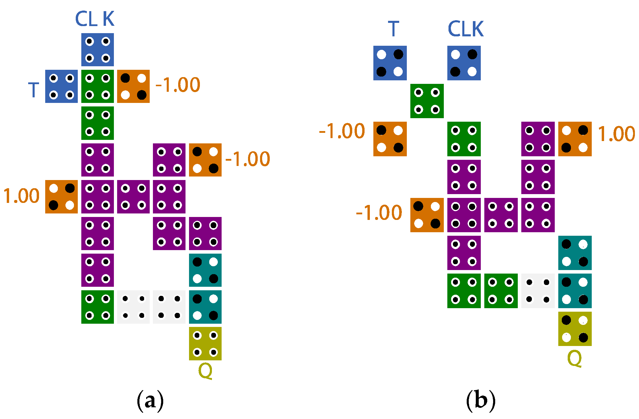
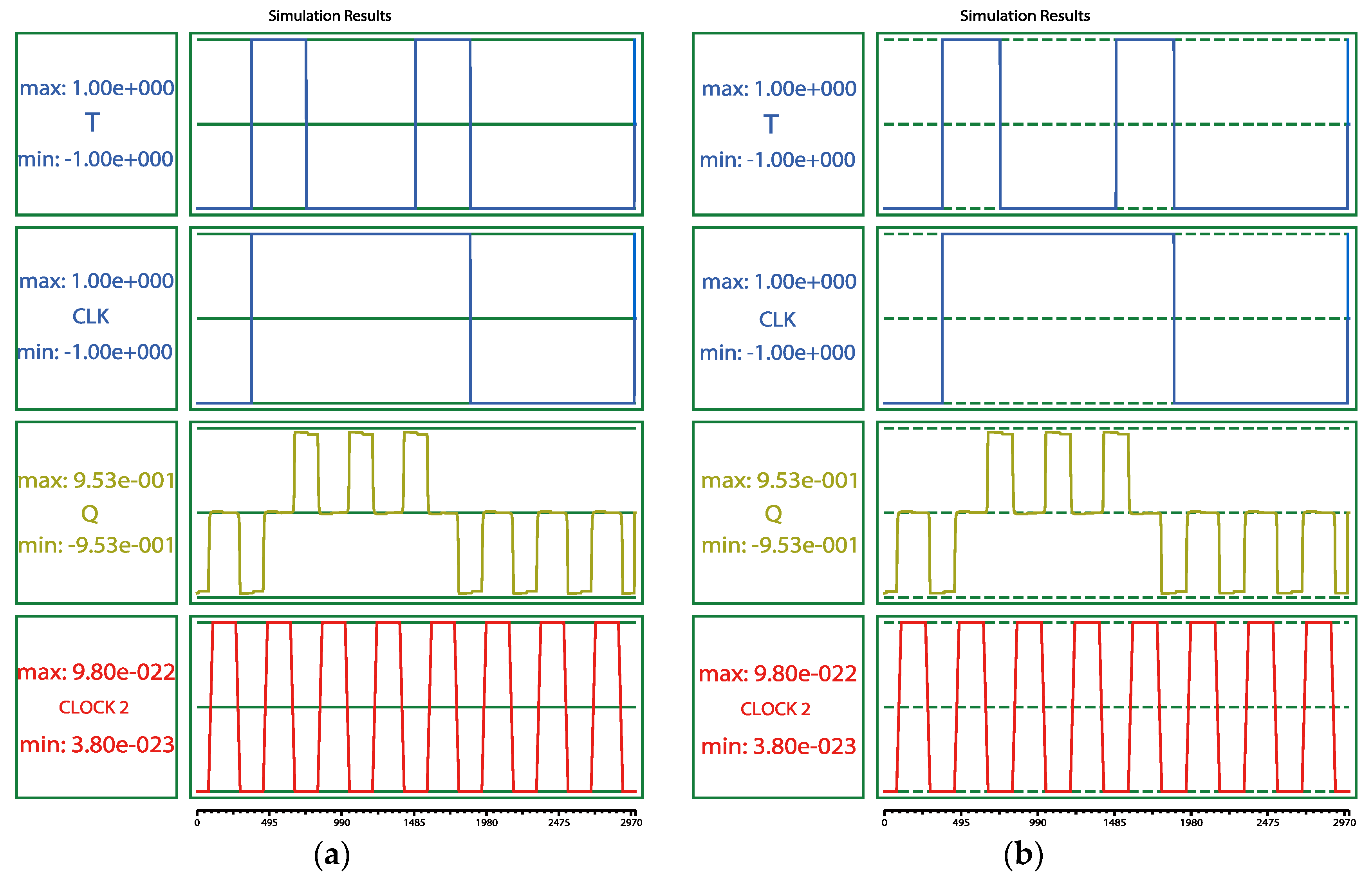
The proposed LST-FFs are sensitive to level signals. Figure 8 shows the two proposed LST-FF circuits (LST-FF1 and LST-FF2). The proposed LST-FF1 is made up of 22 cells. Its area is 17,444 nm2 and its delay is 0.75 clock cycles. The proposed LST-FF2 is made up of 20 cells. Its area is 18644 nm2 and its delay is 0.75 clock cycles. The designs are simulated in QCA Designer. Figure 9 shows the simulation results of the LST-FF circuits. If the clock signal CLK and input signal T are both ‘1’, the current output signal is the complement of the previous output signal; otherwise, the current output signal is the same as the previous output signal.
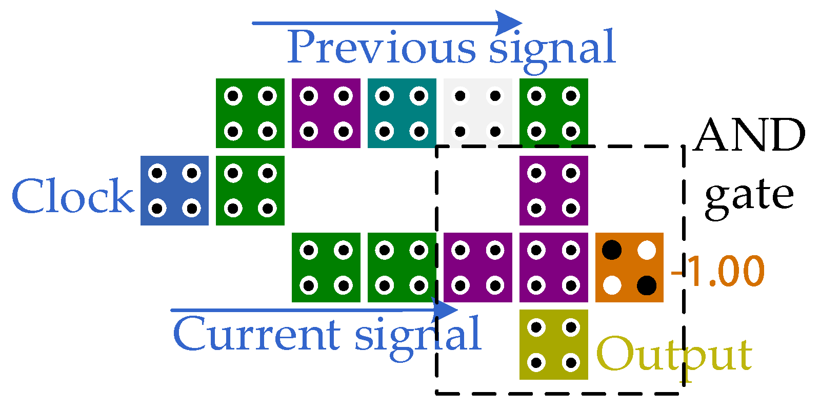
The edge-triggered T flip-flops are implemented by adding an edge detection circuit at the CLK terminal of the LST-FF. The QCA layout of the negative edge detection circuit is shown in Figure 10 and it consists of a looped design and an AND gate [16]. The signal clock is transmitted to two wires (previous signal and current signal). The previous signal is transmitted to an input terminal of the AND gate through a clock cycle. The current signal gets its complementary signal firstly, then it is directly transmitted to another output of the AND gate. The two signals are outputted after an AND operation. The truth table of the negative edge detection circuit is listed in Table 4. According to the truth table, only when the signal clock changes from signal ‘1’ to ‘0’ (i.e., the negative edge is triggered), the negative edge detective circuit can output signal ‘1’, for all other changes of the signal clock, the negative edge detective circuit can output signal ‘0’.
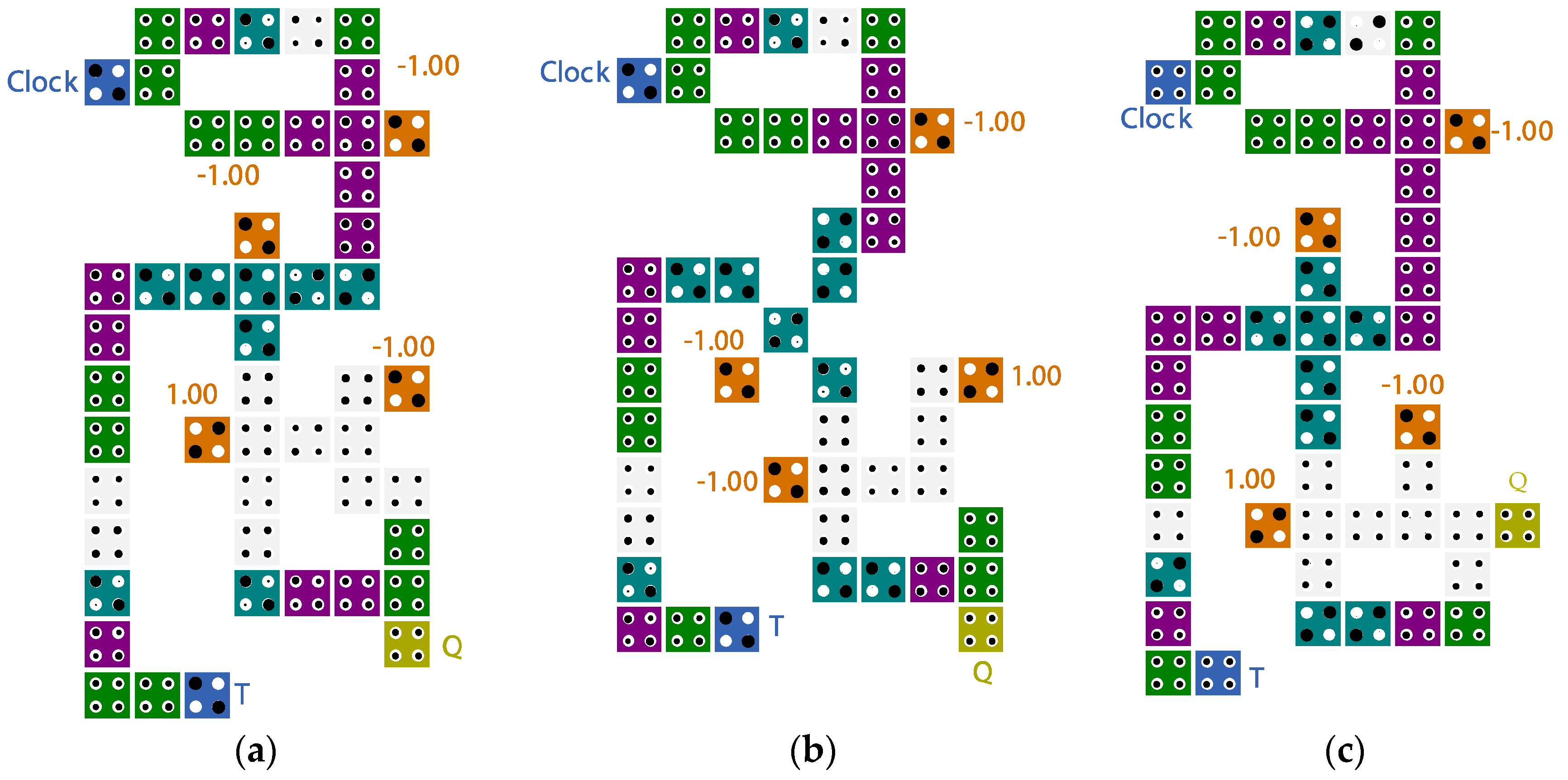
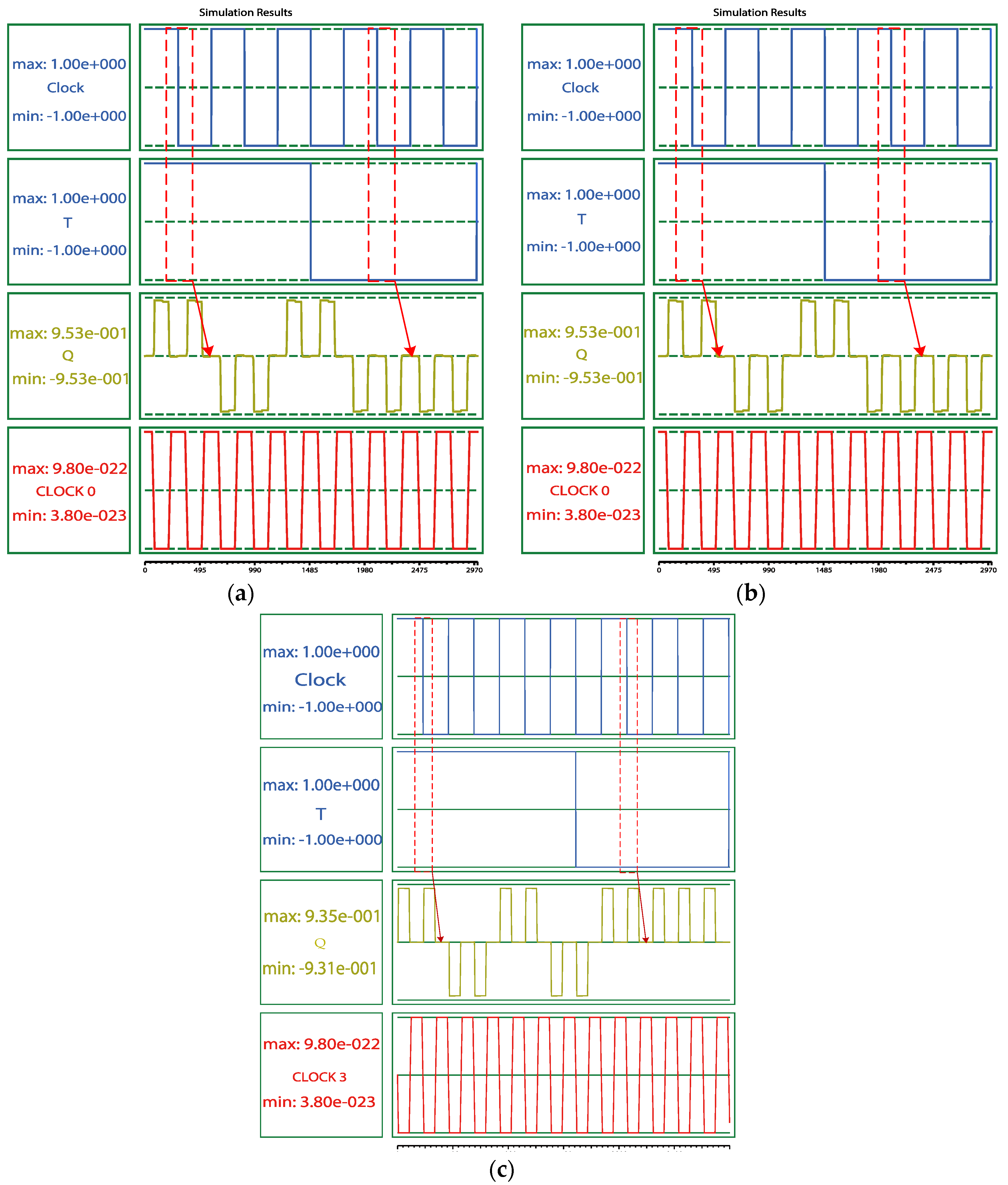
A negative edge-trigger T flip-flop (NET-FF) can be implemented by a negative edge detection circuit and an LST-FF. The negative edge detection circuit detects the changes in the signal clock, and its output state enters into the input terminal CLK of LST-FF. The specific process is as follows: When the negative edge detection circuit is triggered, a signal ‘1’ is transmitted to the CLK signal terminal of LST-FF. If the signal T is ‘1’, the output signal can be reversed; if the signal T is 0, the output signal can keep the previous output state unchanged. When the negative edge detection circuit is not triggered, a signal ‘0’ is transmitted to the input terminal CLK of the LST-FF. If the signal T is 0, the output of LST-FF remains unchanged; if the signal T is 1, the output of LST-FF remains unchanged. The three proposed NET-FFs are shown in Figure 11 (NET-FF1, NET-FF2, and NET-FF3). The NET-FF3 is proposed based on the LST-FF in [16]. The proposed NET-FF1 consists of 50 cells with an area of 38,364 nm2 and a delay of 2.25 clock cycles. The proposed NET-FF2 consists of 47 cells with an area of 40,764 nm2 and a delay of 2.25 clock cycles. The proposed NET-FF3 consists of 49 cells with an area of 43,924 nm2 and a delay of 2 clock cycles. The simulation results in QCA Designer are shown in Figure 12. For the NET-FF1 and NET-FF2, it takes 2.25 clock cycles for data to flow from inputs to output. For the NET-FF3, it takes two clock cycles for data to flow from inputs to output.
Table 5 shows the comparisons of the performance and energy consumption of the existing designs of LST-FFs and NET-FFs. It can be seen from Table 5 that the proposed LST-FF structures are competitive in terms of cell count and area. Compared with other alternative schemes, the proposed second structure has a smaller cell count and lower power consumption. The proposed designs are lower than those designs in [10,11,12,13,14,15] in terms of cell count, area, delay, and power consumption. Compared with the design in [14], the number of cells in the proposed LST-FF2 is reduced by 56.52%, the area is reduced by 66.85%, the delay is reduced by 25%, and the total energy dissipation is reduced by 60.06%. The proposed LST-FF2 uses a three-input majority gate with low fault tolerance. The second proposed design has the disadvantage of low fault tolerance. In the actual environment, the LST-FF structures should be flexibly chosen. The T-FF in [11] does not require fixed inputs but requires two additional inputs (reset and preset inputs). The proposed LST-FFs require three fixed inputs, and the proposed NET-FFs require four fixed inputs. Xiao et al. [35] implemented a dual-edge triggered T flip-flop. Compared with [35], the proposed NET-FFs have a smaller cell count, smaller area, lower latency, and lower power consumption. The area of the proposed NET-FF1 is smaller than that of the proposed NET-FF2, and the energy consumption of the NET-FF2 is smaller than that of the NET-FF1. The latency of NET-FF3 based on the LST-FF proposed in [16] is the lowest.
3.2. Two-to-One Multiplexers and Reversible Gates
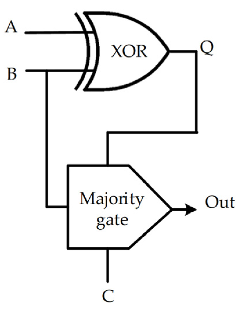
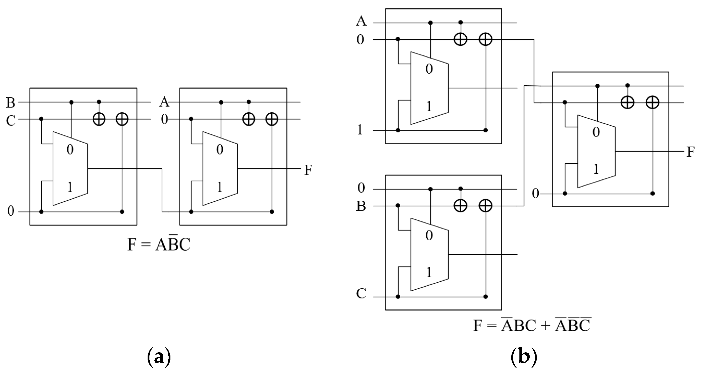
Figure 13 shows the schematic diagram of a two-to-one multiplexer [19]. A two-to-one multiplexer can be implemented by an XOR gate and a three-input majority gate. Signals A and B perform an XOR operation to get the signal Q. Then the signals Q, B, and C enter into the three-input majority gate. Finally, the function of the two-to-one multiplexer is implemented.
Signal A is the control signal, and signals B and C are multiplexed signals. The boolean expression of the two-to-one multiplexer is derived as follows:
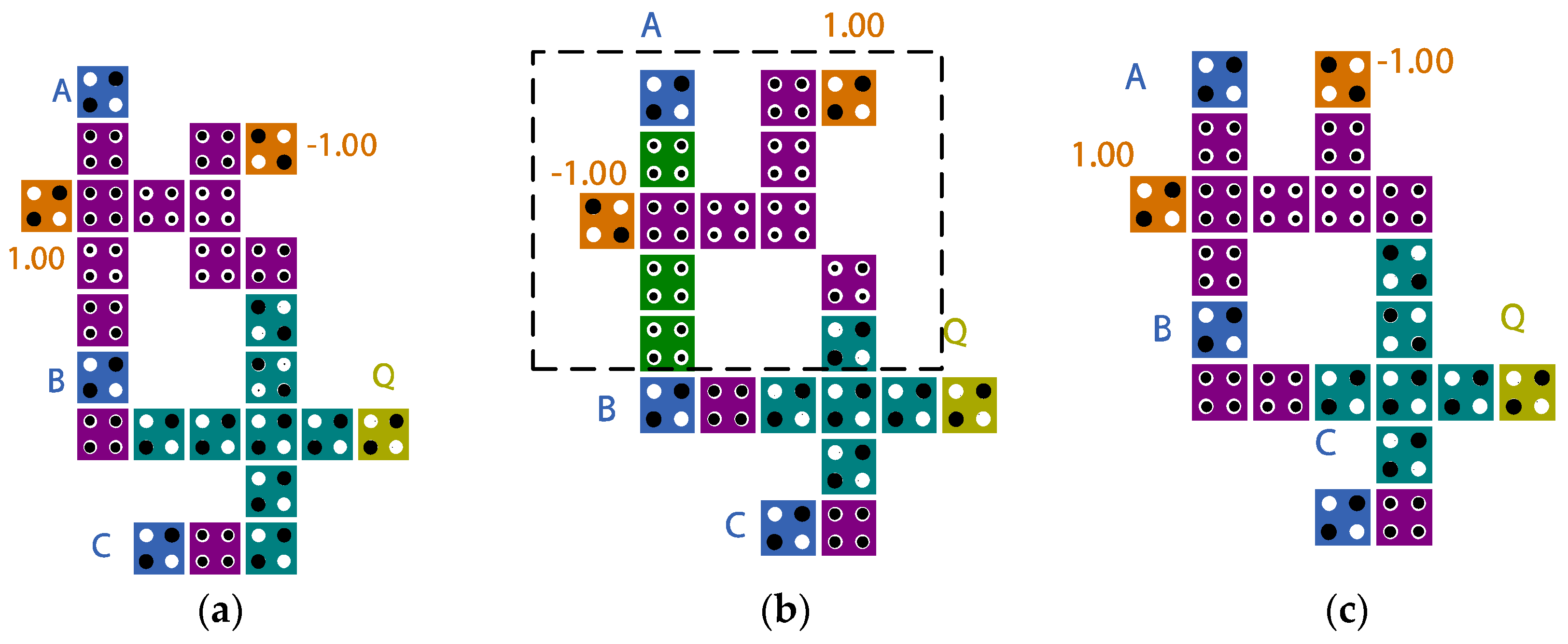
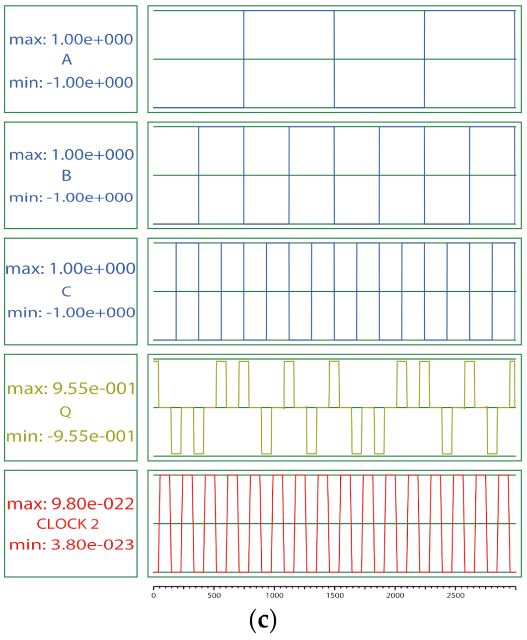
Figure 14 shows the QCA cell layouts of the proposed two-to-one multiplexers (two-to-one MUX1, two-to-one MUX2, and two-to-one MUX3). The XOR gate in the box in Figure 14b is the proposed second XOR gate after adjusting the clock allocation. The proposed two-to-one MUX3 is based on the XOR gate in [5]. The proposed two-to-one MUX1 consists of 25 cells with an area of 24,564 nm2 and a delay of 0.75 clock cycles. The proposed two-to-one MUX2 is composed of 22 cells with an area of 21,804 nm2 and a delay of 0.75 clock cycles. The proposed two-to-one MUX3 is composed of 22 cells with an area of 21,804 nm2 and a delay of 0.75 clock cycles. The proposed two-to-one multiplexers all require two fixed inputs. The designs are simulated in QCA Designer, and the simulation results are shown in Figure 15. When the control signal A is set to ‘0’, the output signal is equal to the input value of signal B (i.e., the two-to-one multiplexer selects signal B to pass). If A is ‘1’ and the output signal is equal to the input value of signal C (i.e., the two-to-one multiplexer selects signal C to pass). It can be seen that the waveforms of the three designs in Figure 15 are correct.
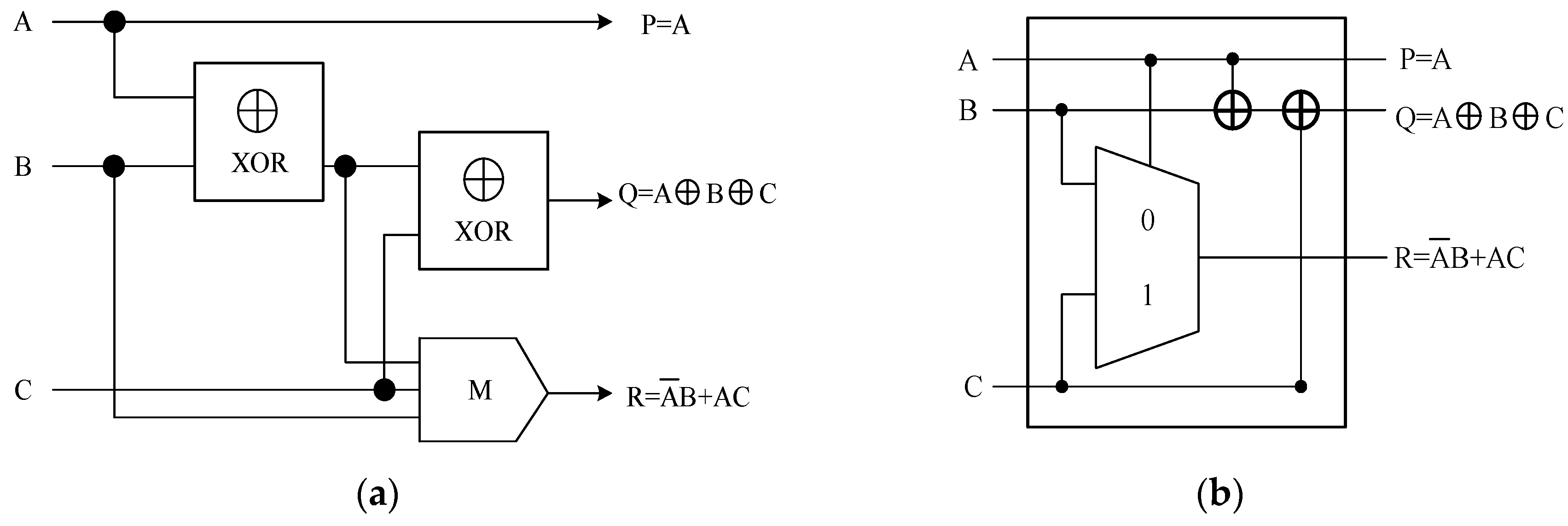
In 2017, Chabi et al. [19] proposed a new reversible gate, and the schematic diagram is shown in Figure 16. The reversible gate requires three inputs and obtains three outputs. The boolean expressions for the three functions are , , and , respectively. The reversible gate can be used for the designs of combinatorial logic circuits. The reversible gate is composed of two XOR gates and a three-input majority gate. The output terminal P is equal to the value of the input signal A. The signal A is directly transmitted to the output terminal P through a wire.
The implementation of output terminal Q is as follows. As shown in Figure 16, signals A and B are transmitted to the first XOR gate for an XOR operation. Then the result and signal C are transmitted to the second XOR gate to implement the XOR operation of the three signals.
The output terminal R implemented the function of the two-to-one multiplexer. The terminal R’s function is implemented by an XOR gate and a three-input majority gate. Signal A is the control signal and B and C are two multiplexed signals. When signal A is low-voltage, signal B is transmitted to the output terminal; when signal A is high-voltage, signal C is transmitted to the output terminal.
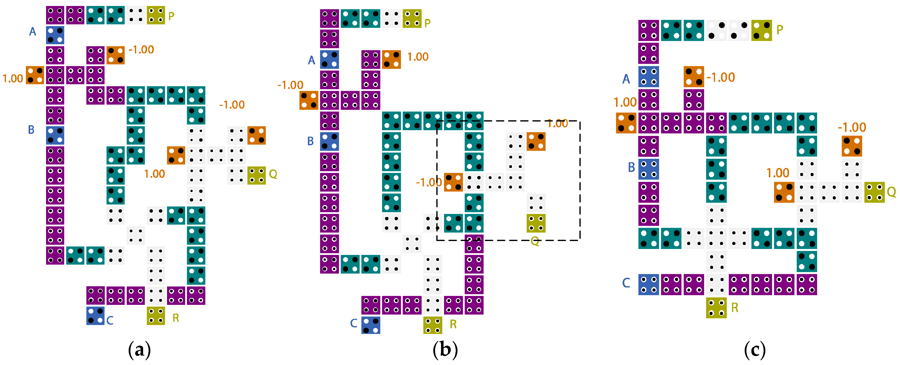
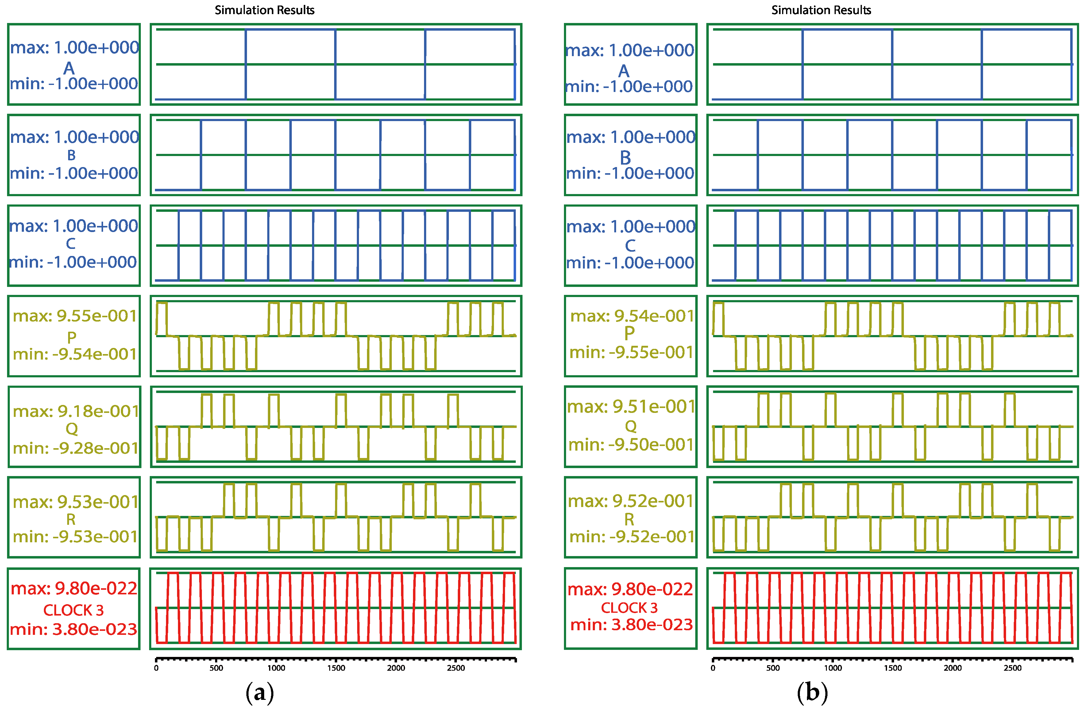
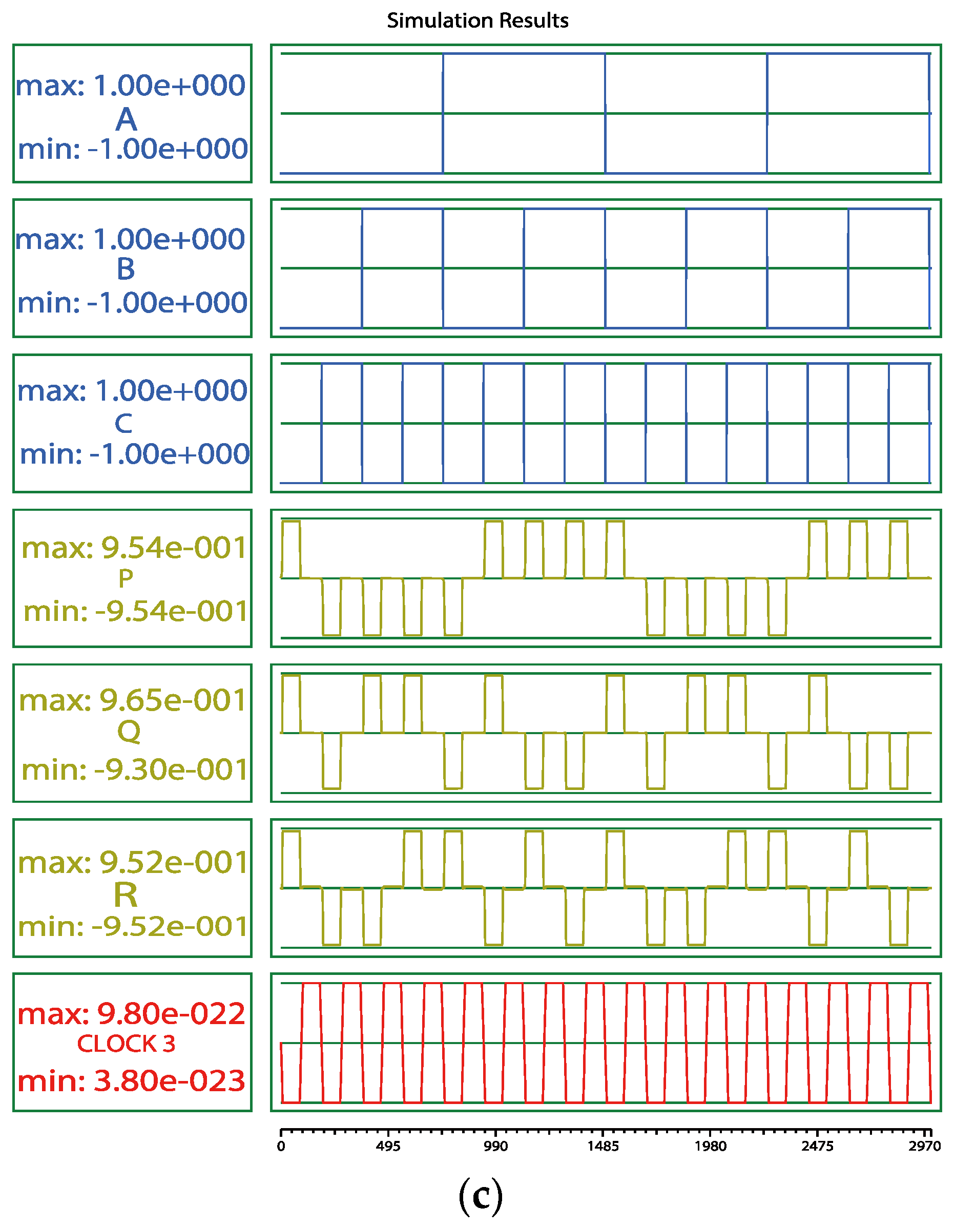
Figure 17 shows the QCA cell layouts of the proposed reversible gates (RG1, RG2, and RG3). The RG3 is implemented by using an existing XOR in [5]. The XOR gate in the box in Figure 17b is the proposed second XOR gate after adjusting the clock allocation which reduces a delay of 0.25 clock cycles. The proposed RG1 gate consists of 68 cells with an area of 0.08 µm2 and a delay of one clock cycle. The proposed RG2 gate consists of 65 cells with an area of 0.08 µm2 and a delay of one clock cycle. The proposed RG3 gate consists of 57 cells with an area of 0.06 µm2 and a delay of one clock cycle. The proposed reversible gates all require four fixed inputs. The designs are simulated in QCA Designer. Figure 18 shows the simulation results of three proposed reversible gates. It can be seen that the waveforms of the three designs in Figure 18 are correct.
The reversible gate can be used to design large combinatorial logic circuits based on boolean functions. Two logic functions are given in Figure 19. The can be implemented by the two reversible gates and the can be implemented by the three reversible gates. Other boolean functions can also be constructed by this reversible gate.
Table 6 shows the comparisons among the existing two-to-one multiplexers. It can be seen from Table 6 that the proposed two-to-one multiplexers have fewer cells compared with [17,18]. Table 7 shows the comparisons between the existing reversible gates. Compared with [19], the cell count and area of the proposed RG1 are reduced by 24.44% and 11.11%, respectively; the cell count and area of the proposed RG2 are reduced by 27.78% and 11.11%, respectively. It can be seen from Table 7 that the cell count and area of the third reversible gate designed using the XOR gate in [5] are the smallest.
Table 8 shows the energy consumption comparisons of alternative two-to-one multiplexers and reversible gates. Only the power consumption of the single-layer designs is considered. It can be seen that the design in [20] is optimal. However, the three-input majority gates of the multiplexer in [20] have low fault tolerance. As can be seen from Table 8, the energy consumption of the proposed two-to-one MUX2 is lower than that design of [19]. The proposed reversible gates are an improvement of the design in [19]. Compared with the energy consumption of the design in [19], the power consumption of the proposed RG2 is lower. The power consumption of the proposed RG1 is higher than that of the design in [19].
3.3. Polar Encoders
In secure communications, encoders and decoders can be implemented by using QCA circuits. Polar code was initially introduced by E. Arikan in 2009 [36]. Polar code is a forward error correction code used for signal transmission. Polar code has explicit proof for the channel performance which has now almost closed the gap to Shannon’s limit and is included as code for the control channels in the 5G standard.
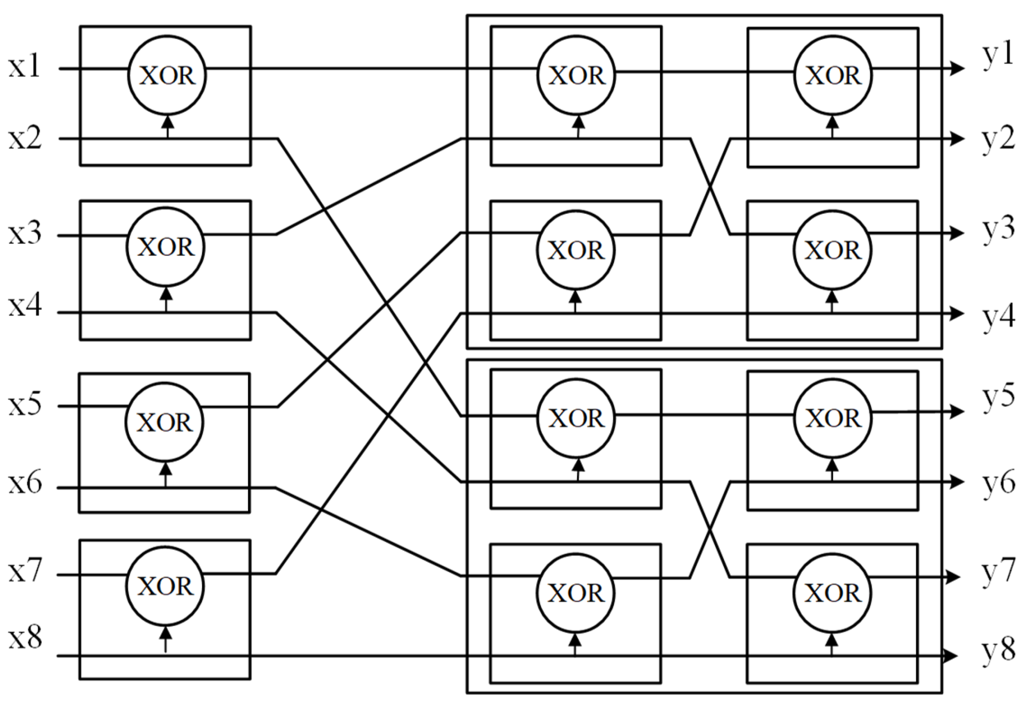
Figure 20 shows the design of polar encoders in the QCA technology proposed by Das et al. [27]. If the inputs x1, x2, x3, and x5 in Figure 20 are set to ‘0’, it can act as an (8, 4) polar encoder (G(8, 4)). Formulas (4)–(11) are boolean expressions for the eight outputs of G(8, 4).
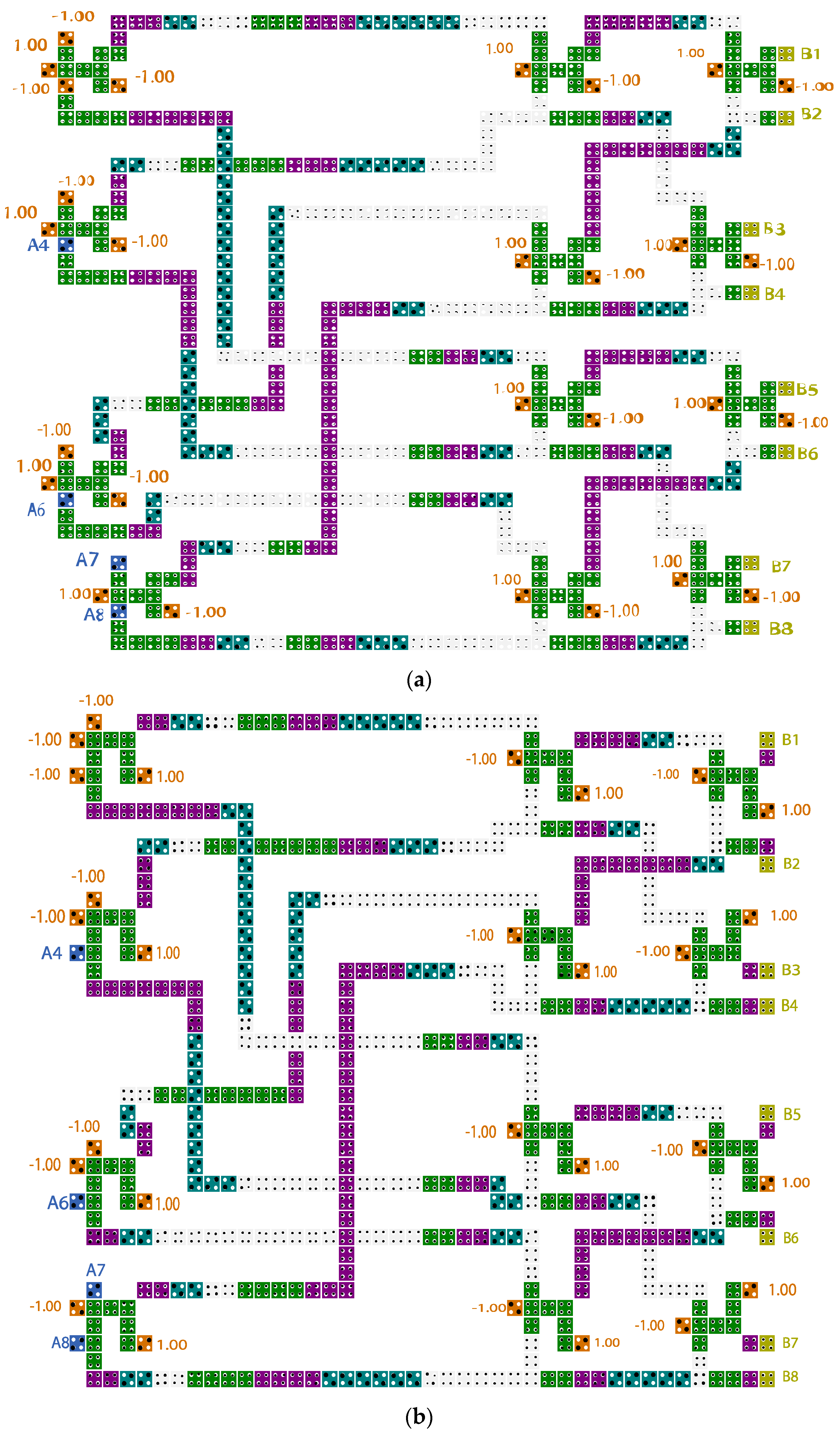
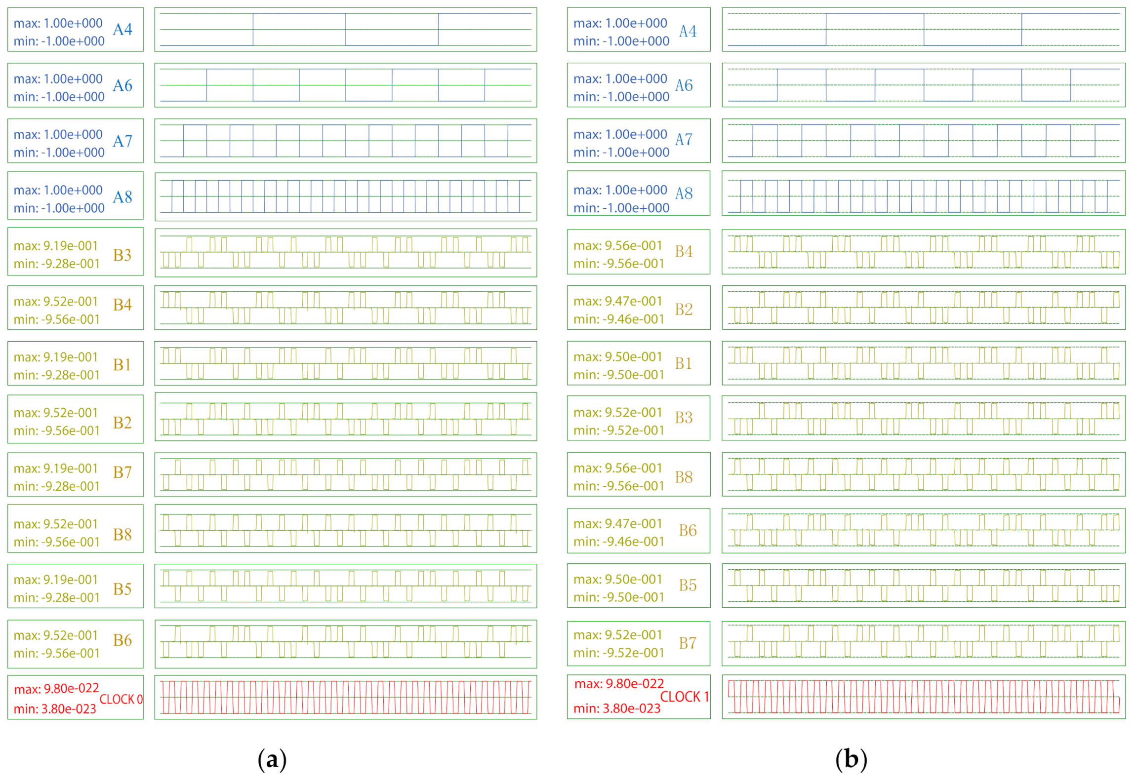
We propose and have implemented the two coplanar G(8, 4) circuits using two proposed XOR gates. Figure 21 shows the layouts of the two proposed G(8, 4) designs. Figure 22 shows the simulation results of the G(8, 4) designs in QCA Designer. The simulation engine of QCA Designer was set to the coherence vector engine, the total simulation time was set to 7.000000e-010 s, and other parameters were set to the default values. The first proposed G(8, 4) consists of 524 cells (see Figure 21a). Its area is 0.685 µm2 and its latency is 3.25 clock cycles. The total and the average energy dissipation of the first proposed G(8, 4) is 1.31 × 10⁻¹ eV and 1.19 × 10⁻² eV. The second proposed G(8, 4) consists of 518 cells (see Figure 21b). Its area is 0.635 µm2 and its latency is 3.50 clock cycles. The total and average energy dissipation of the second proposed G(8, 4) are 1.08 × 10⁻¹ eV and 9.84 × 10⁻³ eV.
Table 9 shows the comparisons of the performance and energy consumption of the two proposed G(8, 4) circuits. The cell count, area, and latency of the proposed G(8, 4) circuits are lower compared with alternative solutions and the second proposed G(8, 4) has the lowest energy dissipation. The two proposed G(8, 4) designs have more external fixed inputs than the design in [28]. In the future, the method proposed by Khosroshahy et al. in [25] can be applied to reduce external fixed inputs of the proposed G(8, 4) designs. Compared with the best solution in [28], the cell count and area of the second proposed G(8, 4) are reduced by 13.67% and 12.05%, respectively, and the latency is reduced by 0.25 clock cycles. Therefore, the two proposed (8, 4) polar encoders, especially the second one, are competitive in terms of cell count, area, and energy consumption.
4. Conclusions
In this paper, two XOR/XNOR gates have been proposed and implemented. Some QCA circuits are designed based on the two proposed XOR/XNOR gates. This work is based on simulation results using QCA Designer and QCA Designer-E. The QCA Designer [29] is one of the widely used QCA simulation tools. The QCA Designer-E [30] can be used to estimate the power consumption of QCA circuits. Compared with the [14], the second proposed LST-FF has fewer cells and lower energy dissipation. The reversible gate in [19] is improved based on two proposed XOR gates and an existing XOR in [5]. The designed reversible gates have the characteristics of small cell count and small area. Compared with the state-of-the-art G(8, 4), the second proposed G(8, 4) has a 13.67% reduction in terms of cell count and a 12.05% reduction in terms of area, also with low energy dissipation. The input signals of the proposed G(8, 4) circuits can output the signals faster due to the reduction in latency. The G(8, 4) circuits are more efficient compared with existing schemes in many evaluating indicators. In the future, our design schemes can be considered to be applied to the design of QCA circuits.
Author Contributions
A.Y. contributed to the formal analysis and methodology, R.L. contributed to the data creation, original draft writing, and simulations, Z.H., P.G. and X.W. contributed to the review and editing. All authors have read and agreed to the published version of the manuscript.
Funding
This research was funded by the National Natural Science Foundation of China under grant 61974001.
Institutional Review Board Statement
Not applicable.
Informed Consent Statement
Not applicable.
Data Availability Statement
Not applicable.
Conflicts of Interest
The authors declare no conflict of interest.
References
- Fortes, J. Future Challenges in VLSI System Design. In Proceedings of the IEEE Computer Society Annual Symposium on VLSI, Tampa, FL, USA, 20–21 February 2003; pp. 5–7. [Google Scholar]
- Chabi, A.; Roohi, A.; DeMara, R.; Angizi, S.; Navi, K.; Khademolhosseini, H. Cost-efficient QCA Reversible Combinational Circuits Based on a New Reversible Gate. In Proceedings of the International Symposium on Computer Architecture and Digital Systems, Tehran, Iran, 7–8 October 2015; pp. 1–6. [Google Scholar]
- Berarzadeh, M.; Mohammadyan, S.; Navi, K.; Bagherzadeh, N. A Novel Low Power Exclusive-OR via Cell Level-based Design Function in Quantum Cellular Automata. J. Comput. Electron. 2017, 16, 875–882. [Google Scholar] [CrossRef]
- Ahmad, F.; Bhat, G.; Khademolhosseini, H.; Azimi, S.; Angizi, S.; Navi, K. Towards Single Layer Quantum-dot Cellular Automata Adders Based on Explicit Interaction of Cells. J. Comput. Sci. 2016, 16, 8–15. [Google Scholar] [CrossRef]
- Chen, H.; Lv, H.; Zhang, Z.; Cheng, X.; Xie, G. Design and Analysis of a Novel Low-power Exclusive-OR Gate Based on Quantum-dot Cellular Automata. J. Circuits Syst. Comput. 2019, 28, 1–17. [Google Scholar] [CrossRef]
- Li, X.; Shao, Z.; Cheng, H.; Jamali Haghighi, M.R. A New Design of QCA-based Nanoscale Multiplexer and Its Usage in Communications. Int. J. Commun. Syst. 2020, 33, 1–12. [Google Scholar]
- Laajimi, R.; Niu, M. Nanoarchitecture of Quantum-Dot Cellular Automata (QCA) Using Small Area for Digital Circuits. Adv. Electron. Circuits–Princ. Archit. Appl. Emerg. Technol. 2018, 67–84. [Google Scholar] [CrossRef] [Green Version]
- Majeed, A.; Zainal, M.; Alkaldy, E.; Nor, D. Single-bit Comparator in Quantum-dot Cellular Automata (QCA) Technology Using Novel QCA-XNOR Gates. J. Electron. Sci. Technol. 2021, 19, 1–11. [Google Scholar] [CrossRef]
- Safaiezadeh, B.; Mahdipour, E.; Haghparast, M.; Sayedsalehi, S.; Hosseinzadeh, M. Design and Simulation of Efficient Combinational Circuits Based on a New XOR Structure in QCA Technology. Opt. Quantum Electron. 2021, 53, 1–16. [Google Scholar] [CrossRef]
- Vetteth, A.; Walus, K.; Dimitrov, V. Quantum-dot Cellular Automata of Flip-flops. ATIPS Lab. 2003, 2500, 1–5. [Google Scholar]
- Torabi, M. A new Architecture for T Flip Flop Using Quantum-dot Cellular Automata. In Proceedings of the IEEE Asia Symposium on Quality Electronic Design, Kuala Lumpur, Malaysia, 19–20 July 2011; pp. 296–300. [Google Scholar]
- Lim, L.; Ghazali, A.; Yan, S.; Chien Fat, C. Sequential Circuit Design Using Quantum-dot Cellular Automata (QCA). In Proceedings of the International Conference on Circuits and Systems, Kuala Lumpur, Malaysia, 3–4 October 2012; pp. 162–167. [Google Scholar]
- Angizi, S.; Navi, K.; Sayedsalehi, S. Efficient Quantum Dot Cellular Automata Memory Architectures Based on the New Wiring Approach. J. Comput. Theor. Nanosci. 2014, 11, 2318–2328. [Google Scholar] [CrossRef]
- Angizi, S.; Moaiyeri, M.; Farrokhi, S.; Navi, K.; Bagherzadeh, N. Designing Quantum-dot Cellular Automata Counters with Energy Consumption Analysis. Microprocess. Microsyst. 2015, 39, 512–520. [Google Scholar] [CrossRef]
- Chakrabarty, R.; Mahato, D.; Banerjee, A.; Choudhuri, S.; Dey, M.; Mandal, N.K. A Novel Design of Flip-flop Circuits Using Quantum Dot Cellular Automata (QCA). In Proceedings of the IEEE Annual Computing and Communication Workshop and Conference, Las Vegas, NV, USA, 8–10 January 2018; pp. 408–414. [Google Scholar]
- Majeed, A.H.; Alkaldy, E.; Zainal, M.; Nor, D.B. Synchronous Counter Design Using Novel Level Sensitive T-FF in QCA Technology. J. Low Power Electron. Appl. 2019, 9, 27. [Google Scholar] [CrossRef] [Green Version]
- Hashemi, S.; Azghadi, M.; Zakerolhosseini, A. A Novel QCA Multiplexer Design. In Proceedings of the International Symposium on Telecommunications, Tehran, Iran, 27–28 August 2008; pp. 692–696. [Google Scholar]
- Sabbaghi-Nadooshan, R.; Kianpour, M. A Novel QCA Implementation of MUX-based Universal Shift Register. J. Comput. Electron. 2014, 13, 198–210. [Google Scholar] [CrossRef]
- Chabi, A.; Roohi, A.; Khademolhosseini, H.; Sheikhfaal, S.; Angizi, S.; Navi, K.; DeMara, R.F. Towards Ultra-efficient QCA Reversible Circuits. Microprocess. Microsyst. 2017, 49, 127–138. [Google Scholar] [CrossRef]
- Ahmad, F. An Optimal Design of QCA Based 2n: 1/1: 2n Multiplexer/Demultiplexer and Its Efficient Digital Logic Realization. Microprocess. Microsyst. 2018, 56, 64–75. [Google Scholar] [CrossRef]
- Ma, X.; Huang, J.; Metra, C.; Lombardi, F. Testing Reversible 1D Arrays for Molecular QCA. In Proceedings of the IEEE International Symposium on Defect and Fault Tolerance in VLSI Systems, Arlington, VA, USA, 4–6 October 2006; pp. 71–79. [Google Scholar]
- Sen, B.; Saran, D.; Saha, M.; Sikdar, B.P. Synthesis of Reversible Universal Logic Around QCA with Online Testability. In Proceedings of the International Symposium on Electronic System Design, Kochi, India, 19–21 December 2011; pp. 236–241. [Google Scholar]
- Sen, B.; Dutta, M.; Goswami, M.; Sikdar, B.K. Modular Design of Testable Reversible ALU by QCA Multiplexer with Increase in Programmability. Microelectron. J. 2014, 45, 1522–1532. [Google Scholar] [CrossRef]
- Khosroshahy, M.; Abdoli, A.; Panahi, M. Novel Feynman-Based Reversible and Fault-Tolerant Nano-communication Arithmetic Architecture Based on QCA Technology. SN Comput. Sci. 2021, 2, 1–14. [Google Scholar]
- Khosroshahy, M.; Moaiyeri, M.; Angizi, S.; Bagherzadeh, N.; Navi, K. Quantum-dot Cellular Automata Circuits with Reduced External Fixed Inputs. Microprocess. Microsyst. 2017, 50, 154–163. [Google Scholar] [CrossRef]
- Khosroshahy, M.; Abdoli, A.; Rahmani, A. Design and Power Analysis of an Ultra-high Speed Fault-tolerant Full-adder Cell in Quantum-dot Cellular Automata. Int. J. Theor. Phys. 2022, 61, 1–19. [Google Scholar]
- Das, J.; De, D. QCA Based Design of Polar Encoder Circuit for Nano Communication Network. Nano Commun. Netw. 2018, 18, 82–92. [Google Scholar] [CrossRef]
- Ahmed, S.; Naz, S.; Bhat, S. Design of Quantum-dot Cellular Automata Technology Based Cost-efficient Polar Encoder for Nanocommunication Systems. Int. J. Commun. Syst. 2020, 33, 1–21. [Google Scholar]
- Walus, K.; Dysart, T.; Jullien, G.; Budiman, R.A. QCADesigner: A Rapid Design and Simulation Tool for Quantum-dot Cellular Automata. IEEE Trans. Nanotechnol. 2004, 3, 26–31. [Google Scholar] [CrossRef]
- Torres, F.; Wille, R.; Niemann, P.; Drechsler, R. An Energy-aware Model for the Logic Synthesis of Quantum-dot Cellular Automata. IEEE Trans. Comput.-Aided Des. Integr. Circuits Syst. 2018, 37, 3031–3041. [Google Scholar] [CrossRef]
- Gin, A.; Tougaw, P.; Williams, S. An Alternative Geometry for Quantum-dot Cellular Automata. J. Appl. Phys. 1999, 85, 8281–8286. [Google Scholar] [CrossRef]
- Shin, S.; Jeon, J.; Yoo, K. Wire-crossing Technique on Quantum-dot Cellular Automata. In Proceedings of the 2nd International Conference on Next Generation Computer and Information Technology, Las Vegas, NV, USA, 15–17 April 2013; pp. 52–57. [Google Scholar]
- Bhanja, S.; Ottavi, M.; Lombardi, F.; Pontarelli, S. Novel Designs for Thermally Robust Coplanar Crossing in QCA. Des. Autom. Test. Eur. 2006, 1, 1–6. [Google Scholar]
- Khosroshahy, M.; Daliri, M.; Abdoli, A.; Navi, K.; Bagherzadeh, N. A 3D Universal Structure Based on Molecular-QCA and CNT Technologies. J. Mol. Struct. 2016, 1119, 86–95. [Google Scholar] [CrossRef]
- Xiao, L.; Xu, X.; Ying, S. Dual-edge Triggered T Flip-flop Structure Using Quantum-dot Cellular Automata. Adv. Mater. Res. 2013, 662, 562–567. [Google Scholar] [CrossRef]
- Arikan, E. Channel Polarization: A Method for Constructing Capacity-achieving Codes for Symmetric Binary-input Memoryless Channels. IEEE Trans. Inf. Theory 2009, 55, 3051–3073. [Google Scholar] [CrossRef]
Figure 1.
QCA basic units. (a) QCA cell (1, −1), (b) inverter, and (c) three-input majority gate.

Figure 2.
QCA clock.

Figure 3.
Crosswires. (a) Multilayer crosswire, (b) coplanar crosswire implemented by rotating QCA cells in [31], (c) coplanar crosswire implemented by QCA cells in clock zones 1 and 3 in [32], and (d) coplanar crosswire implemented by QCA cells in clock zones 2 and 4 in [32].

Figure 4.
The existing XOR/XNOR gates. (a) [2], (b) [3], (c) [4], (d) [5], (e) [6], (f) [7], (g) [8], and (h) [9].

Figure 5.
Proposed XOR/XNOR gates. (a)The first XOR gate (XOR1), (b) the first XNOR gate (XNOR1), (c) the second XOR gate (XOR2), (d) the second XNOR gate (XNOR2), (e) the I/O access method for the first design, (f) the I/O access method for the second design and (g) the I/O access method for the second design.

Figure 6.
Simulation results of the proposed XOR/XNOR gates. (a) The first XOR gate (XOR1), (b) the first XNOR gate (XNOR1), (c) the second XOR gate (XOR2), and (d) the second XNOR gate (XNOR2).
Figure 6.
Simulation results of the proposed XOR/XNOR gates. (a) The first XOR gate (XOR1), (b) the first XNOR gate (XNOR1), (c) the second XOR gate (XOR2), and (d) the second XNOR gate (XNOR2).

Figure 7.
Schematic diagram of an LST-FF [16].
Figure 7.
Schematic diagram of an LST-FF [16].

Figure 8.
Proposed level-sensitive T flip-flops (LST-FFs). (a) The first LST-FF (LST-FF1) and (b) the second LST-FF (LST-FF2).
Figure 8.
Proposed level-sensitive T flip-flops (LST-FFs). (a) The first LST-FF (LST-FF1) and (b) the second LST-FF (LST-FF2).

Figure 9.
Simulation results of the proposed LST-FF circuits. (a) The first LST-FF (LST-FF1) and (b) the second LST-FF (LST-FF2).
Figure 9.
Simulation results of the proposed LST-FF circuits. (a) The first LST-FF (LST-FF1) and (b) the second LST-FF (LST-FF2).

Figure 10.
Negative edge detection circuit [16].
Figure 10.
Negative edge detection circuit [16].

Figure 11.
The proposed negative edge-trigger T flip-flops (NET-FFs). (a) The first NET-FF (NET-FF1), (b) the second NET-FF (NET-FF2), and (c) the third NET-FF implemented by using the LST-FF in [16] (NET-FF3).
Figure 11.
The proposed negative edge-trigger T flip-flops (NET-FFs). (a) The first NET-FF (NET-FF1), (b) the second NET-FF (NET-FF2), and (c) the third NET-FF implemented by using the LST-FF in [16] (NET-FF3).

Figure 12.
The simulation results of proposed NET-FFs. (a) NET-FF1, (b) NET-FF2, and (c) NET-FF3.

Figure 13.
Schematic diagram of a 2-to-1 multiplexer [19].
Figure 13.
Schematic diagram of a 2-to-1 multiplexer [19].

Figure 14.
Layouts of the proposed 2-to-1 multiplexers: (a) 2-to-1 MUX1, (b) 2-to-1 MUX2, and (c) 2-to-1 MUX3 implemented by using the XOR in [5].
Figure 14.
Layouts of the proposed 2-to-1 multiplexers: (a) 2-to-1 MUX1, (b) 2-to-1 MUX2, and (c) 2-to-1 MUX3 implemented by using the XOR in [5].

Figure 15.
Simulation results of the proposed 2-to-1 multiplexers: (a) 2-to-1 MUX1, (b) 2-to-1 MUX2, and (c) 2-to-1 MUX3.
Figure 15.
Simulation results of the proposed 2-to-1 multiplexers: (a) 2-to-1 MUX1, (b) 2-to-1 MUX2, and (c) 2-to-1 MUX3.


Figure 16.
Schematic diagram of a reversible gate in [19]. (a) schematic diagram and (b) symbol.
Figure 16.
Schematic diagram of a reversible gate in [19]. (a) schematic diagram and (b) symbol.

Figure 17.
Layouts of the proposed reversible gates. (a) the first reversible gate (RG1), (b) the second reversible gate (RG2), and (c) the third reversible gate implemented by using the XOR in [5] (RG3).
Figure 17.
Layouts of the proposed reversible gates. (a) the first reversible gate (RG1), (b) the second reversible gate (RG2), and (c) the third reversible gate implemented by using the XOR in [5] (RG3).

Figure 18.
Simulation results of the proposed reversible gates. (a) The first reversible gate (RG1), (b) the second reversible gate (RG2), and (c) the third reversible gate implemented by using the XOR in [5] (RG3).
Figure 18.
Simulation results of the proposed reversible gates. (a) The first reversible gate (RG1), (b) the second reversible gate (RG2), and (c) the third reversible gate implemented by using the XOR in [5] (RG3).


Figure 19.
Logic functions implemented by the reversible gate in [19]. (a) ; (b) .
Figure 19.
Logic functions implemented by the reversible gate in [19]. (a) ; (b) .

Figure 20.
Schematic diagram of a polar encoder [27].
Figure 20.
Schematic diagram of a polar encoder [27].

Figure 21.
The QCA implementation of the proposed G(8, 4) circuits. (a) the first G(8, 4) and (b) the second G(8, 4).
Figure 21.
The QCA implementation of the proposed G(8, 4) circuits. (a) the first G(8, 4) and (b) the second G(8, 4).

Figure 22.
Simulation results of the proposed G(8, 4) circuits. (a) The first G(8, 4) and (b) the second G(8, 4).
Figure 22.
Simulation results of the proposed G(8, 4) circuits. (a) The first G(8, 4) and (b) the second G(8, 4).


Table 1.
Advantages and disadvantages of alternative XOR/XNOR gates.
| Design | Advantages | Disadvantages |
|---|---|---|
| [2] | Low latency, Easy access I/O | High energy consumption, Large area |
| [3] | Low latency, Easy access I/O | High energy consumption, Large area |
| [4] | Low latency, Easy access I/O | High energy consumption, Large area |
| [5] | Small cell count, Low latency, Low power consumption, Easy access I/O | Low fault tolerance |
| [6] | Low latency, Easy access I/O | High energy consumption, Large area |
| [7] | Small area | High energy consumption |
| [8] | Low latency | High energy consumption |
| [9] | Small cell count, Easy access I/O | High energy consumption |
Table 2.
The default parameters for the coherence vector simulation engine in QCA Designer.
| Simulation Engine | Coherence Vector |
|---|---|
| Temperature | 1.00 K |
| Relaxation Time | 1.00 × 10⁻¹⁵ s |
| Time Step | 1.00 × 10⁻¹⁶ s |
| Cell size | 18 nm × 18 nm |
| Gap of cell | 2 nm |
| Radius of Effect | 80 nm |
| Clock High | 9.8 × 10⁻²² J |
| Clock Low | 3.8 × 10⁻²³ J |
| Clock Shift | 0 |
| Total Simulation Time | 7.00 × 10⁻¹¹ s |
| Relative Permittivity | 12.9 |
| Layer Separation | 11.5 nm |
Table 3.
Comparisons of the performance and energy dissipation for alternative XOR/XNOR gates.
| Design | Cell Count | Area (nm2) | Latency | Number of Fixed Inputs | Total Energy Dissipation (eV) | Average Energy Dissip Ation (eV) |
|---|---|---|---|---|---|---|
| [2] | 14 | 11,564 | 0.25 | 3 | 1.17 × 10⁻² | 1.07 × 10⁻³ |
| [3] | 13 | 11,564 | 0.50 | 3 | 8.06 × 10⁻³ | 7.33 × 10⁻⁴ |
| [4] | 14 | 16,284 | 0.50 | 1 | 1.44 × 10⁻² | 1.31 × 10⁻³ |
| [5] | 9 | 7644 | 0.25 | 2 | 3.56 × 10⁻³ | 3.24 × 10⁻⁴ |
| [6] | 13 | 13,524 | 0.50 | 2 | 8.02 × 10⁻³ | 7.29 × 10⁻⁴ |
| [7] | 10 | 5684 | 0.50 | 1 | 9.78 × 10⁻³ | 8.89 × 10⁻⁴ |
| [8] | 12 | 9604 | 0.25 | 1 | 1.07 × 10⁻² | 9.76 × 10⁻⁴ |
| [9] | 10 | 6084 | 0.50 | 1 | 1.13 × 10⁻² | 1.02 × 10⁻³ |
| Pro-XOR/XNOR1 | 11 | 7644 | 0.25 | 2 | 6.21 × 10⁻³ | 5.64 × 10⁻⁴ |
| Pro-XOR/XNOR2 | 11 | 9204 | 0.50 | 2 | 4.13 × 10⁻³ | 3.75 × 10⁻⁴ |
Table 4.
Negative edge trigger truth table.
| Previous Clock | Current Clock | Output |
|---|---|---|
| 0 | 0 | 0 |
| 1 | 0 | 1 |
| 0 | 1 | 0 |
| 1 | 1 | 0 |
Table 5.
Comparisons of the performance and energy dissipation for alternative LST-FFs and NET-FFs.
| Design | Cell Count | Area (nm2) | Latency | Number of Fixed Inputs | Total Energy Dissipation (eV) | Average Energy Dissipation (eV) |
|---|---|---|---|---|---|---|
| [10] | 92 | 99,524 | 1.25 | 5 | 3.47 × 10⁻² | 3.16 × 10⁻³ |
| [11] | 66 | 60,164 | 1.25 | 0 | 2.12 × 10⁻² | 1.92 × 10⁻³ |
| [12] | 108 | 198,204 | 1.5 | 3 | 4.20 × 10⁻² | 3.82 × 10⁻³ |
| [13] | 55 | 59,004 | 1.50 | 4 | 2.06 × 10⁻² | 1.87 × 10⁻³ |
| [14] | 46 | 56,244 | 1.00 | 4 | 1.71 × 10⁻² | 1.55 × 10⁻³ |
| [15] | 81 | 66,564 | 1.50 | 6 | 3.42 × 10⁻² | 3.11 × 10⁻³ |
| [16] | 21 | 18,644 | 0.50 | 3 | 6.99 × 10⁻³ | 6.36 × 10⁻⁴ |
| Pro-LST-FF1 | 22 | 17,444 | 0.75 | 3 | 7.88 × 10⁻³ | 7.16 × 10⁻⁴ |
| Pro-LST-FF2 | 20 | 18,644 | 0.75 | 3 | 6.83 × 10⁻³ | 6.21 × 10⁻⁴ |
| [35] | 184 | 317,604 | 3 | 6 | 6.34 × 10⁻² | 5.77 × 10⁻³ |
| Pro-NET-FF1 | 50 | 38,364 | 2.25 | 4 | 1.66 × 10⁻² | 1.51 × 10⁻³ |
| Pro-NET-FF2 | 47 | 40,764 | 2.25 | 4 | 1.26 × 10⁻² | 1.14 × 10⁻³ |
| Pro-NET-FF3 | 49 | 43,924 | 2 | 4 | 1.60 × 10⁻² | 1.45 × 10⁻³ |
Table 6.
Comparisons of the performance for alternative 2-to-1 multiplexers.
| Design | Cell Count | Area (µm2) | Latency | Number of Fixed Inputs | Layer Type |
|---|---|---|---|---|---|
| [17] | 36 | 0.06 | 1 | 3 | multilayer |
| [18] | 26 | 0.02 | 0.5 | 2 | coplanar |
| [19] | 23 | 0.02 | 0.75 | 3 | coplanar |
| [20] | 16 | 0.01 | 0.5 | 2 | coplanar |
| Pro 2-to-1 MUX1 | 25 | 0.02 | 0.75 | 2 | coplanar |
| Pro 2-to-1 MUX2 | 22 | 0.02 | 0.75 | 2 | coplanar |
| Pro 2-to-1 MUX3 | 22 | 0.02 | 0.75 | 2 | coplanar |
Table 7.
Comparisons of the performance for alternative reversible gates.
| Design | Cell Count | Area (µm2) | Latency | Number of Fixed Inputs | Layer Type |
|---|---|---|---|---|---|
| Fredkin [21] | 246 | 0.37 | 1 | 6 | coplanar |
| RUG [22] | 297 | 0.46 | 2 | 6 | coplanar |
| RM [23] | 224 | 0.25 | 1 | 10 | coplanar |
| [19] | 90 | 0.09 | 1 | 6 | coplanar |
| Pro-RG1 | 68 | 0.08 | 1 | 4 | coplanar |
| Pro-RG2 | 65 | 0.08 | 1 | 4 | coplanar |
| Pro-RG3 | 57 | 0.06 | 1 | 4 | coplanar |
Table 8.
Comparisons of the energy dissipation for alternative 2-to-1 multiplexers and reversible gates.
Table 8.
Comparisons of the energy dissipation for alternative 2-to-1 multiplexers and reversible gates.
| Design | Total Energy Dissipation (eV) | Average Energy Dissipation (eV) |
|---|---|---|
| [18] | 1.19 × 10⁻² | 1.08 × 10⁻³ |
| [19] | 1.76 × 10⁻² | 1.60 × 10⁻³ |
| [20] | 1.07 × 10⁻² | 9.71 × 10⁻⁴ |
| Pro 2-to-1 MUX1 | 2.21 × 10⁻² | 2.01 × 10⁻³ |
| Pro 2-to-1 MUX2 | 1.58 × 10⁻² | 1.44 × 10⁻³ |
| Pro 2-to-1 MUX3 | 1.59 × 10⁻² | 1.45 × 10⁻³ |
| [19] | 2.20 × 10⁻² | 2.00 × 10⁻³ |
| Pro-RG1 | 2.64 × 10⁻² | 2.40 × 10⁻³ |
| Pro-RG2 | 2.17 × 10⁻² | 1.98 × 10⁻³ |
| Pro RG 3 | 2.58 × 10⁻² | 2.35 × 10⁻³ |
Table 9.
Comparisons of the performance and energy dissipation for alternative (8, 4) polar encoders.
Table 9.
Comparisons of the performance and energy dissipation for alternative (8, 4) polar encoders.
| Design | Cell Count | Area (µm2) | Latency | Number of Fixed Inputs | Total Energy Dissipation (eV) | Average Energy Dissipation (eV) |
|---|---|---|---|---|---|---|
| [27] | 1188 | 1.915 | 6.25 | 40 | 3.29 × 10⁻¹ | 2.99 × 10⁻² |
| [28] | 600 | 0.722 | 3.75 | 16 | 1.13 × 10⁻¹ | 1.02 × 10⁻² |
| Proposed1 | 524 | 0.685 | 3.25 | 28 | 1.31 × 10⁻¹ | 1.19 × 10⁻² |
| Proposed2 | 518 | 0.635 | 3.50 | 28 | 1.08 × 10⁻¹ | 9.84 × 10⁻³ |
Publisher’s Note: MDPI stays neutral with regard to jurisdictional claims in published maps and institutional affiliations. |
© 2022 by the authors. Licensee MDPI, Basel, Switzerland. This article is an open access article distributed under the terms and conditions of the Creative Commons Attribution (CC BY) license (https://creativecommons.org/licenses/by/4.0/).
Share and Cite
MDPI and ACS Style
Yan, A.; Liu, R.; Huang, Z.; Girard, P.; Wen, X. Designs of Level-Sensitive T Flip-Flops and Polar Encoders Based on Two XOR/XNOR Gates. Electronics 2022, 11, 1658. https://0-doi-org.brum.beds.ac.uk/10.3390/electronics11101658
AMA Style
Yan A, Liu R, Huang Z, Girard P, Wen X. Designs of Level-Sensitive T Flip-Flops and Polar Encoders Based on Two XOR/XNOR Gates. Electronics. 2022; 11(10):1658. https://0-doi-org.brum.beds.ac.uk/10.3390/electronics11101658
Chicago/Turabian StyleYan, Aibin, Runqi Liu, Zhengfeng Huang, Patrick Girard, and Xiaoqing Wen. 2022. "Designs of Level-Sensitive T Flip-Flops and Polar Encoders Based on Two XOR/XNOR Gates" Electronics 11, no. 10: 1658. https://0-doi-org.brum.beds.ac.uk/10.3390/electronics11101658
Note that from the first issue of 2016, this journal uses article numbers instead of page numbers. See further details here.