
Design of 2.5D Miniaturized Broadband Absorber for Ultrahigh-Frequency Band


School of Integrated Circuits and Electronics, Beijing Institute of Technology, Beijing 100081, China
*
Author to whom correspondence should be addressed.
Electronics 2022, 11(10), 1664; https://0-doi-org.brum.beds.ac.uk/10.3390/electronics11101664
Submission received: 24 April 2022
/
Revised: 19 May 2022
/
Accepted: 20 May 2022
/
Published: 23 May 2022
(This article belongs to the Section Circuit and Signal Processing)
Abstract
:A broadband metamaterial absorber (MA) structure for Ultrahigh-Frequency (UHF) band was proposed, and the miniaturization of the unit was realized by combining the method of bending metal wires and loading metal vias. The size of the unit cell is 0.040 λL × 0.040 λL × 0.075 λL (λL is the wavelength corresponding to the lowest frequency of 0.5 GHz). The simulation results show that the bandwidth of the MA is from 0.50 GHz to 1.33 GHz, and the relative bandwidth is 90.7%. Polarization insensitivity of the MA was realized through assembling a 2 × 2 orthogonal array. TE and TM polarizations maintain more than 80% of the absorptance in the range of 40° at oblique incidence. The consistency of full-wave simulation, circuit simulation and measured results is high, which verifies the broadband absorption characteristics of the proposed MA.
1. Introduction
Since Landy successfully designed the first MA [1], rich research results of MAs have been accumulated in terms of structural forms and design principles. However, current researches on stealth materials mainly focus on X and Ku bands [2,3,4], while researches on UHF band are less. It is because the attenuation constant of the material decreases significantly at low frequency, and the electrical size corresponding to the low frequency is relatively large, which is difficult to meet the need for miniaturization in practical applications.
Combined with current research, the low-frequency technology of MAs can be divided into two categories. One is to lower the position of the resonance point by lumped elements, and the other is to use the convolution geometry method to increase the length of metal wire by bending, winding, etc. In 2017, Xuan K B et al. proposed a design method of absorbers loaded by capacitors [5]. Four lumped capacitors embedded between metal patches effectively lower the resonant frequency. Experimental results show that the structure achieves perfect absorption at 102 MHz, and the unit size is reduced to 35 × 35 mm2. Then, in order to verify the contribution of capacitors to the resonant frequency regulation, two capacitors with different capacitance values were loaded into the unit [6] so that the MA realized double absorption peaks at 304.9 MHz and 358.5 MHz. Inductors were also applied in low-frequency technology research of MAs. Jeong H et al. [7] connected the metal square ring with four inductors and indicated that the absorption frequency was inversely proportional to the inductance value of the inductors. In addition, Buitung S innovatively proposed an hourglass-type absorber structure on the basis of curved lines [8], which can obtain a narrow-band absorption peak near 377 MHz. Araneo R et al. designed a complex helical unit structure by using tightly arranged helical lines to enhance the coupling effect in MA [9] and achieved perfect absorption at 395 MHz. Although the above designs achieve low-frequency absorption, it is a common problem that the bandwidths of designed MAs are not wide enough. In 2016, a compact MA for the UHF band was designed in [10], and it bends the square metal ring loaded with resistors inward several times. Without affecting the frequency response, it reduces the unit size to a quarter of the metal square ring, but the absolute bandwidth of the MA is only 150 MHz. In order to improve the bandwidth, the bending method of metal wires, the number of lumped resistors and the thickness of the air layer were further optimized in [11], thereby introducing more resonance points in MA. The research successfully realizes a low-frequency broadband MA operating from 0.8 GHz to 2.7 GHz.
The above research results enrich the design ideas of low-frequency MAs, but they are all optimized based on traditional 2D structures. In recent years, 3D structures [12,13] and 2.5D structures [14,15,16,17] have been widely used in the design of metamaterials. Unlike 3D structures, 2.5D structures show wide-band and low-frequency characteristics without changing the profile height. Typical structures of 2.5D are proposed in [14,15]. Metal vias can increase the capacitance and inductance in the equivalent circuit. In addition, it can connect a longer circuit in MA, which is conducive to the realization of low-frequency. With a systematic study of the equivalent circuit with metal vias [16], Yi-min et al. introduced vertical vias into the design of frequency selective surface and proposed the calculation formula of equivalent capacitance and equivalent inductance. In addition, the research verifies the great potential of metal vias in low-frequency characteristics through simulation and measurement. On this basis, 36 metal vias were introduced in MA, further reducing the resonant frequency to 1890 MHz [17].
In this paper, a MA structure for the UHF band based on 2.5D is proposed, which can achieve more than 90% absorptance in the range from 500 MHz to 1330 MHz. We established a simplified equivalent circuit model and verified the simulation results experimentally. According to simulation and measurement results, the proposed MA achieves the comprehensive performance of wide-band, miniaturization, low frequency and low profile. On the one hand, it can effectively reduce electromagnetic interference and improve the complex electromagnetic environment. Thus, it can improve stability when applied to UHF-RFID systems. In addition, the proposed MA can also be applied to the field of stealth in the UHF band, absorbing electromagnetic waves reflected in the environment to achieve perfect stealth.
2. Unit Cell Design and Simulation
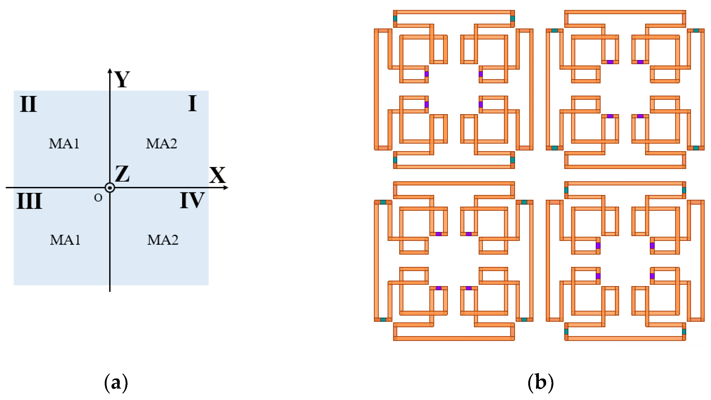
By combining the methods of bending lines and metal vias, a 2.5D double-layer MA unit was proposed. As shown in Figure 1a, layers composing the unit structure from top to bottom are Metal-Layer I, Dielectric-Layer I, Metal-Layer II, Dielectric-Layer II, Metal-Layer III, Air-Layer and Reflection-Layer. Figure 1b,c show the structures of the three Metal-Layers. The structures of Metal-Layer I and Metal-Layer III are completely the same, and they are orthogonal to Metal-Layer II in the middle. The purple and green patches in Figure 1b are resistors with values Ra = 91 Ω and Rb = 100 Ω. It can be seen that resistors are only designed on the Metal-Layer I and the Metal-Layer III. This is because the Metal-Layer II is located between the double Dielectric-Layers, and it is not suitable to load lumped elements with thickness during the fabrication. Metal-Layers are arranged on the upper and lower surfaces of the Dielectric-Layers and connected by multiple metal vias to form a closed loop in Figure 1d. Unlike 3D structures, the introduction of vias does not increase the profile height of the MA, so it is called a 2.5D structure. Metal holes passing through the Dielectric-Layers connect the upper and lower circuits, and it means that metal patches can be designed as longer loops in the same unit, increasing the level of miniaturization of MA.
Figure 1e shows the multi-layer structure of the MA unit cell. In order to achieve better low-frequency characteristics, the MA is laminated with double FR4 (εr1 = 4.4, tanδ = 0.2) Dielectric-Layers, and the thickness of the single Dielectric-Layer is h1/2 = 2.4 mm. The Air-Layer (εr0 = 1.0) with a thickness of h0 = 40 mm is located between the Dielectric-Layer and the Reflection-Layer, which is conducive to the realization of broadband matching with free space. Due to the symmetry of the MA, we only marked geometry dimensions of one-eighth of the bend line on the top view of Figure 1f. Simulation settings of the MA in HFSS are shown in Figure 1a. The MA is excited by a floquet port, and the sides of the unit are set to the master and slave boundary. The geometric parameters in MA were adjusted to achieve the best broadband characteristics, and the final geometric dimensions are optimized as: a1 = 8.4 mm, a2 = 5.6 mm, a3 = 2.4 mm, a4 = 6.6 mm, b1 = 2.4 mm, b2 = 5.6 mm and b3 = 4 mm. In addition, the period of the MA is p = 23.8 mm, and the width of the wire is w = 0.5 mm.
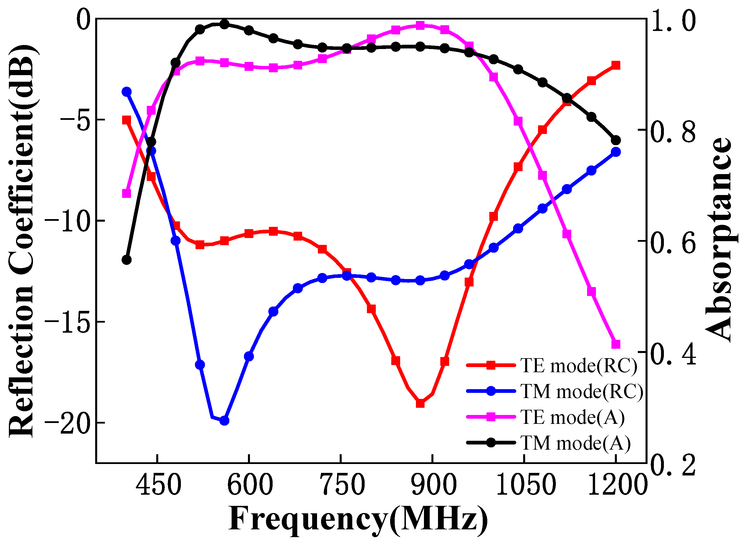
Simulation results of the MA are shown in Figure 2. Due to the existence of the Reflection-Layer, the absorptance can be calculated by . It can be seen that the bandwidth of TE mode is 0.47 GHz to 1.00 GHz, and that of TM mode is 0.47 GHz to 1.06 GHz. The absorption peaks are formed around 550 MHz and 880 MHz in both modes, but trends of reflection coefficient curves are quite different. It is because three Metal-Layers are not completely identical. Generally speaking, such MAs without quadruple rotational symmetry are polarization-sensitive.
Next, we further eliminated the polarization sensitivity of the MA by forming arrays. As shown in Figure 3, we rotated the MA1 along the Z-axis to obtain the orthogonal unit MA2 and stagger them on a 2 × 2 array. MA1 and MA2 have negligible phase differences to plane incident waves under infinite-period boundary conditions. Therefore, the arrayed MAs can produce nearly equal absorption for TE and TM modes when the array scale is large enough.
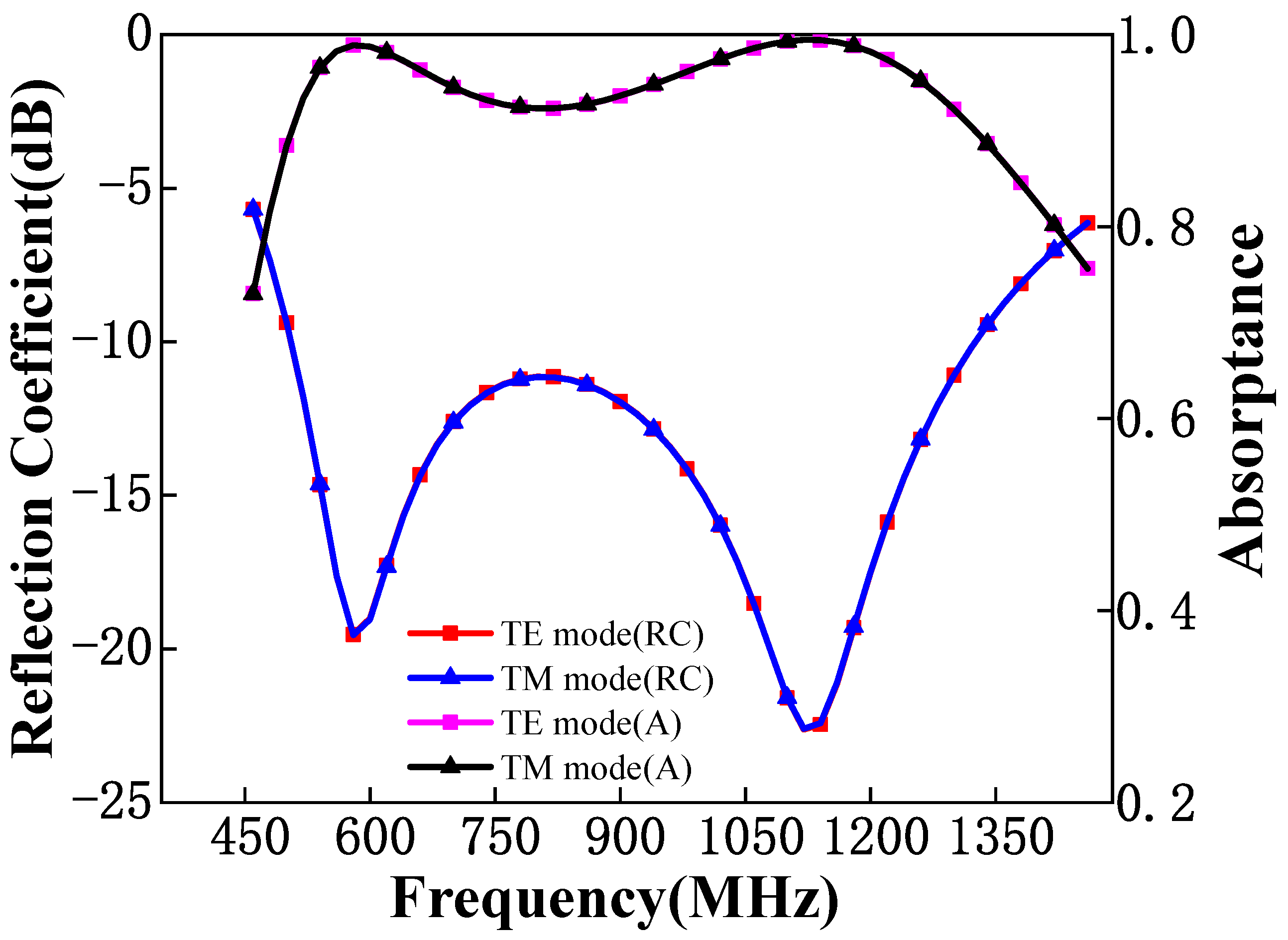
From the simulation results in Figure 4, the bandwidth of the proposed structure meeting the requirements of the absorptance above 90% is 500 MHz to 1330 MHz, and the relative bandwidth is 90.7%. The MA unit cell is miniaturized through wire bending. The unit cell size is 23.8 mm × 23.8 mm, and the profile height is 44.8 mm. Two absorption peaks of the arrayed MA are formed at FL = 0.59 GHz and FH = 1.13 GHz with reflection coefficients of −19.6 dB and −22.7 dB and absorptance of 98.9% and 99.5%. It is due to the blocking effect of resistors with different resistance values, which cuts the closed-loop into current paths of different lengths, which can further adjust the position of FL and FH to realize broadband absorption at low frequency. It can be seen that the curves at different polarizations basically coincide, and the arrayed MAs achieve polarization insensitivity.
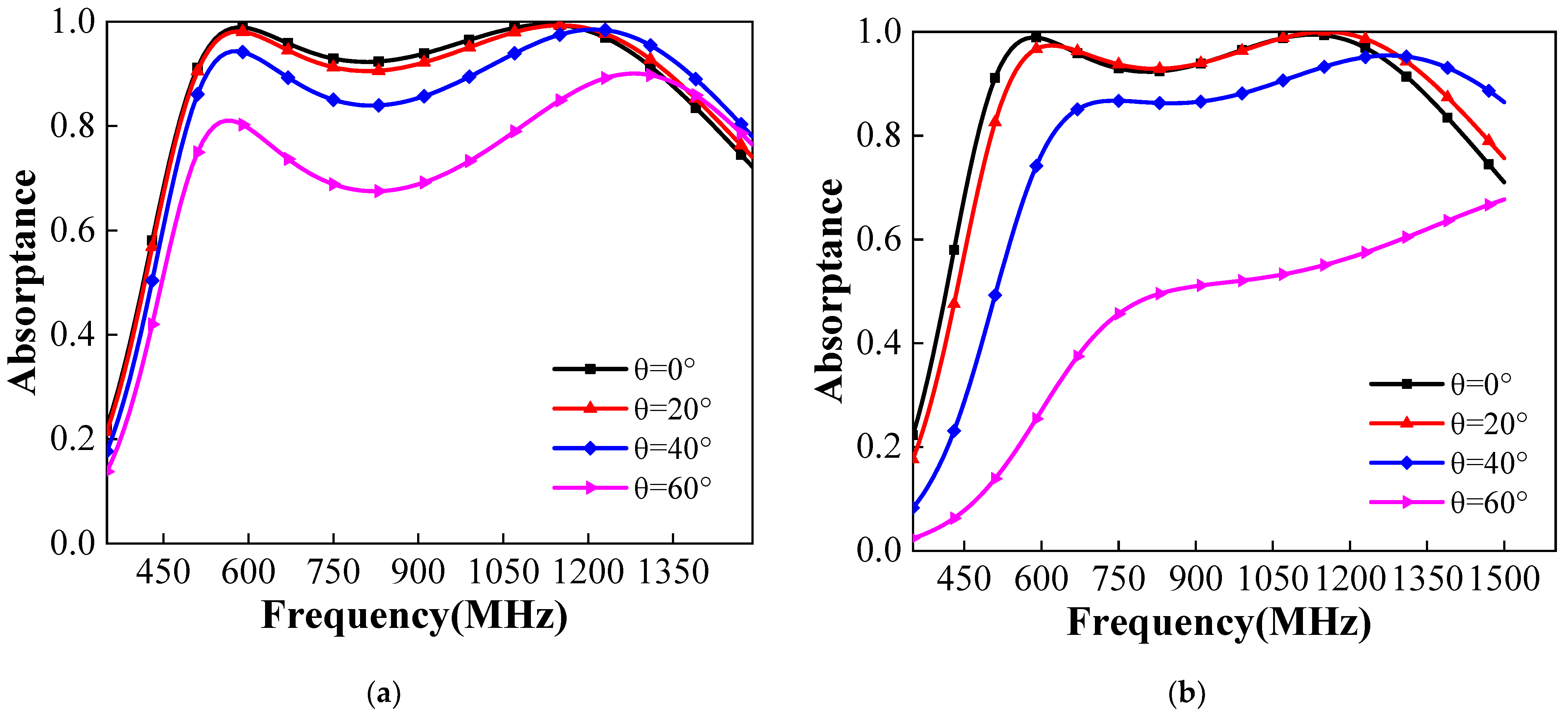
Figure 5 shows the simulated absorptance curves of TE and TM polarizations at different oblique incident angles. As shown in Figure 5a, with the increase in oblique incident angle, the position of FL in TE polarization basically does not change, while FH gradually moves slightly to a high frequency. In addition, the absorptance gradually decreased within the bandwidth, and the depression between FL and FH gradually deepened. Different from TE polarization, the absorption curve of TM polarization has a more obvious blue shift under oblique incidence, and the low-frequency characteristics are gradually lost. In general, the 2.5D structure maintains more than 80% of the absorptance under the incident angle of 40° and has good oblique incidence stability.
3. Absorption Mechanism
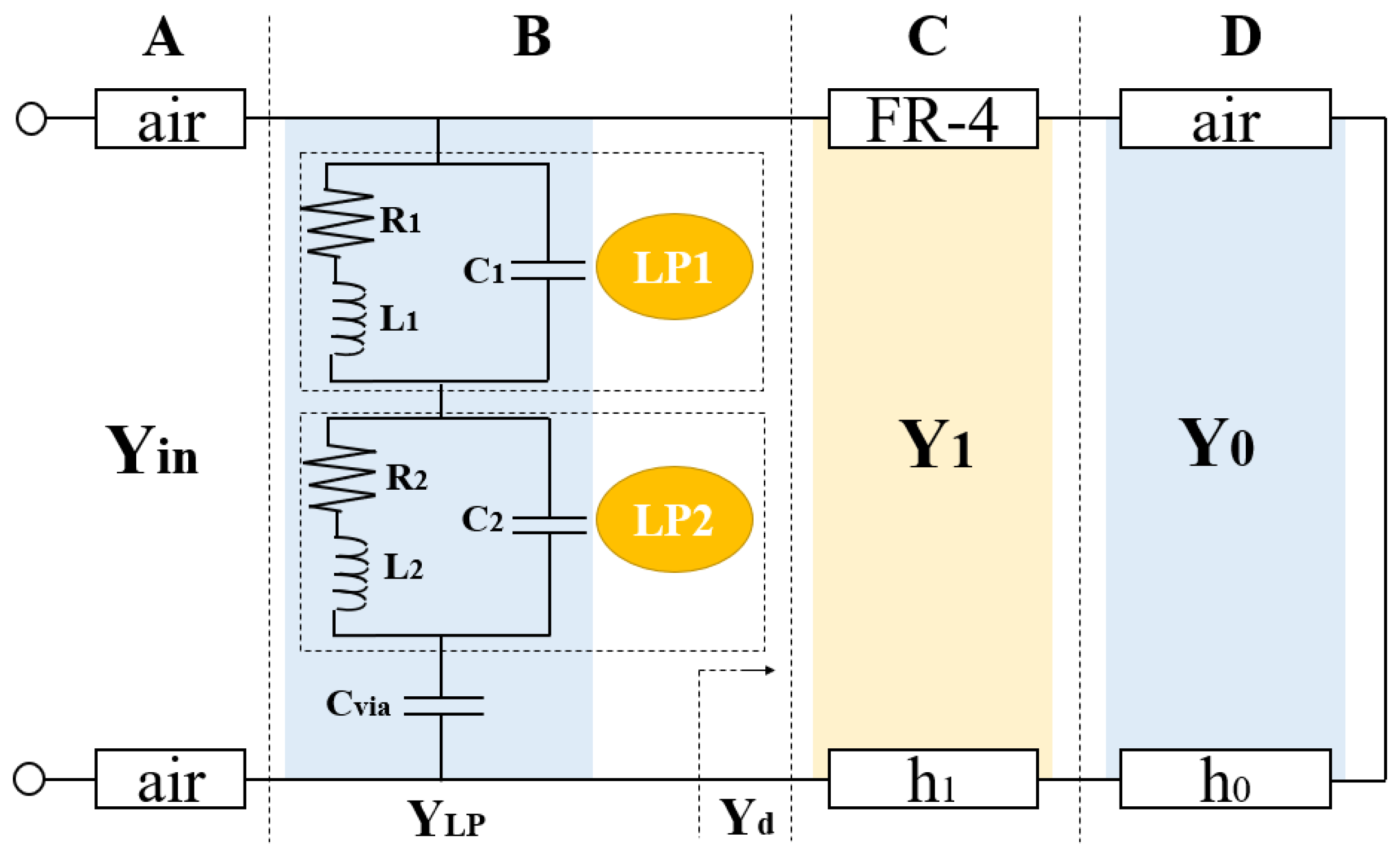
We proposed a simplified equivalent circuit model based on transmission-line theory. As shown in Figure 6, the bent metal wire is composed of two parallel resonant loops in series. The Dielectric-Layer and Air-Layer are equivalent to uniform transmission lines, and the Reflection-Layer is represented by a short-circuit line.
Section A in Figure 6 represents the transmission line in free space, which characteristic impedance is Z0 = 377 Ω, and the electromagnetic wave of normal incidence enters the surface of the MA through A. Section B is the Metal-Layers in MA. LP1 and LP2 loops generate low and high-frequency resonance points, respectively, whose admittances are represented by YLP1 and YLP2. The coupling effect of metalized vias between adjacent units is represented by the supplementary capacitance Cvia. Sections C and D are equivalently modeling the Dielectric-Layer and Air-Layer. Sections C simulates a transmission line with characteristic impedance Z1 and length h1. Sections D simulates a transmission line with characteristic impedance Z0 and length h0.
The admittances of LP1, LP2 loops and Cvia are expressed as follows.
so
According to transmission-line theory, Yd is expressed as
Y0 and Y1 are the admittance forms corresponding to the characteristic impedances Z0 and Z1. The admittance corresponding to the input impedance Zin of the MA can be expressed as.
where, , , . According to the transmission-line theory mentioned above, the reflection coefficients of the model at discrete points are calculated in ADS, and the simulation results of each discrete point are fitted into a smooth reflection coefficient curve. Then, the parameter values of the lumped elements in the circuit model are optimized to achieve the minimum error between the circuit and the full-wave simulations. The circuit component values in the model are optimized as follows: R1 = 85 Ω, C1 = 0.85 pF, L1 = 18 nH, R2 = 60 Ω, C1 = 0.20 pF, L1 = 3.6 nH and Cvia = 1.20 pF. To verify the accuracy of the model, we compare the results of ADS circuit simulation and HFSS full-wave simulation in Figure 7. The results show that the variation trend of the absorption curve in bandwidth is consistent with the full-wave simulation. The working bandwidth of the circuit simulation is 515 MHz to 1310 MHz, and the positions of the two absorption peaks basically coincide.
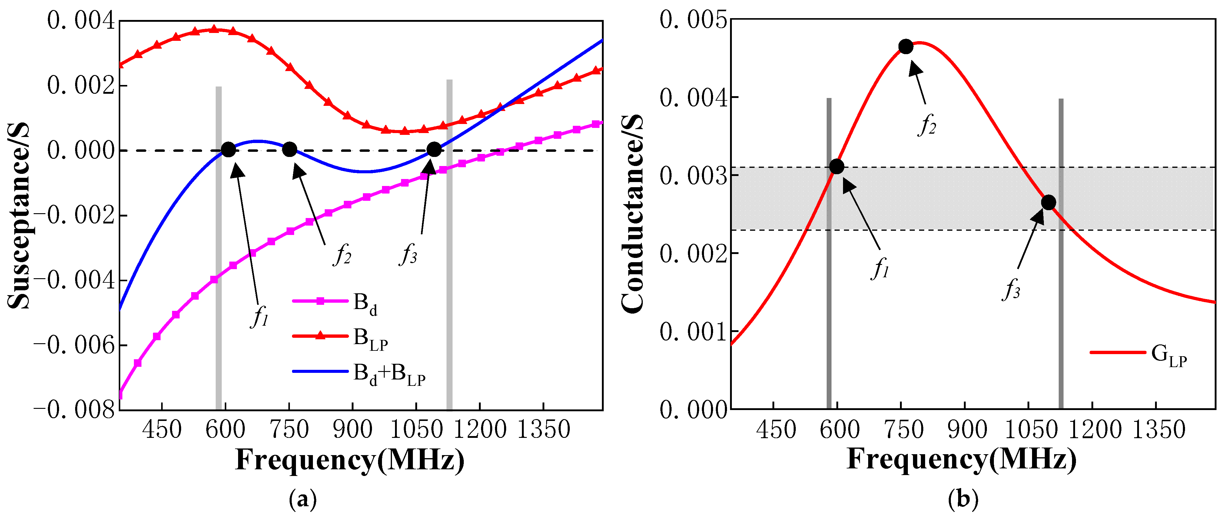
In order to further understand the generation mechanism of the double resonance point, we studied the real and imaginary parts of Yin in the equivalent circuit. According to Equations (4) to (6), we plotted the curves of GLP, Bd, BLP and Bd plus BLP in Figure 8. It can be seen in Figure 8a that the sum of Bd and BLP is 0 at f1 = 600 MHz, f2 = 762 MHz and f3 = 1089 MHz, which means that the imaginary part of Yin is 0. In general, the real part of the impedance that can generate resonance should match Z0, and the conductance range corresponding to (377 ± 50) Ω is marked in the gray part shown in Figure 8b. The conductance of f1 and f3 are within the matching range of the free space, which is basically consistent with FL and FH in full-wave simulation. However, the GLP at f2 is about 0.005, corresponding to a characteristic impedance of about 200 Ω. It is quite different from the characteristic impedance of free space, resulting in a mismatch, so there is no absorption peak at f2.
4. Experiment Results and Discussions
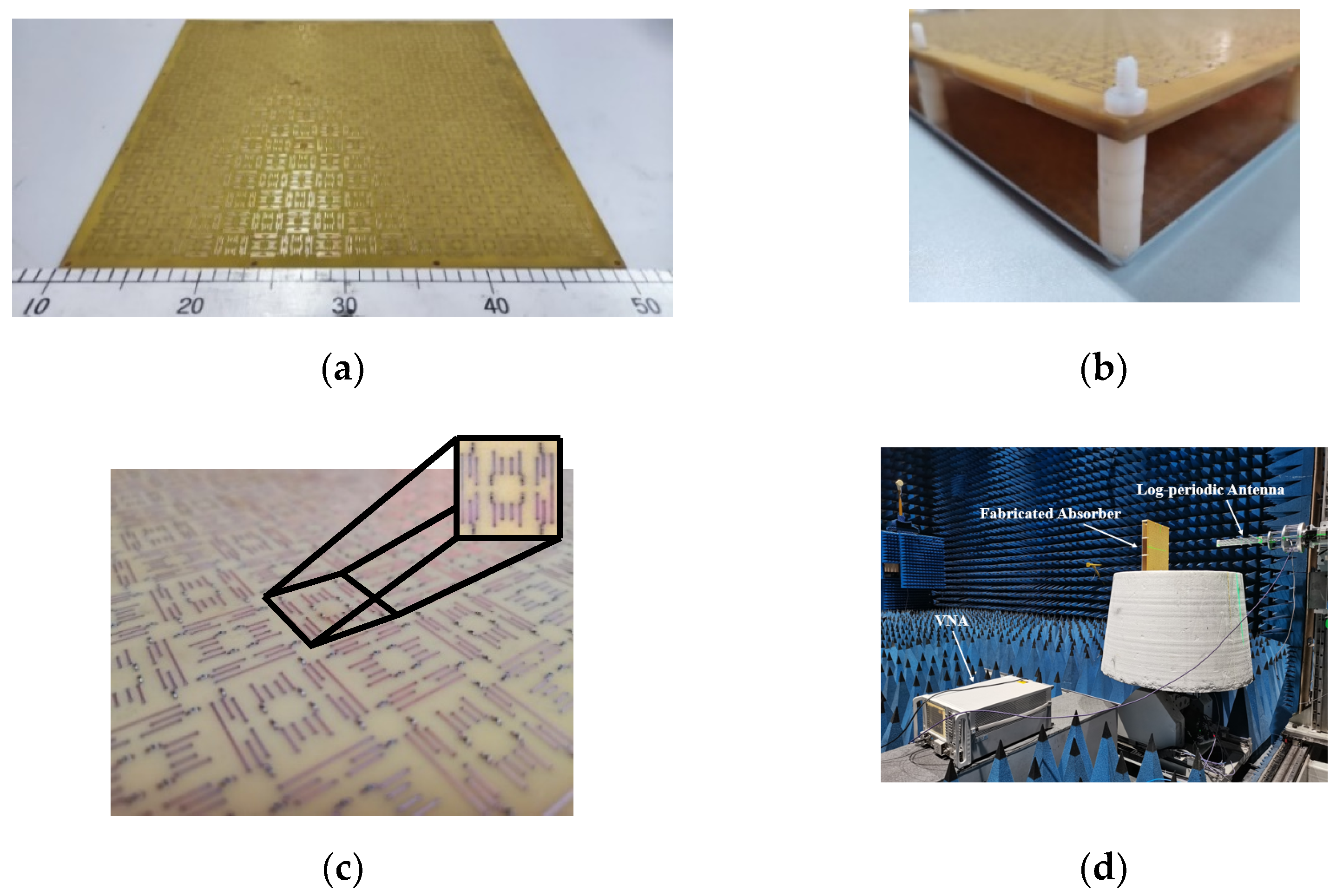
As shown in Figure 9a,b, the MA is fabricated with a dimension of 400 mm × 400 mm (16 cells × 16 cells), and Teflon nuts and bolts are used to control the thickness of the air gap. The measurement system of the fabricated absorber is shown in Figure 9d, and the reflection coefficient of the sample in free space was measured with a log-periodic antenna operating from 0.4 GHz to 3 GHz.
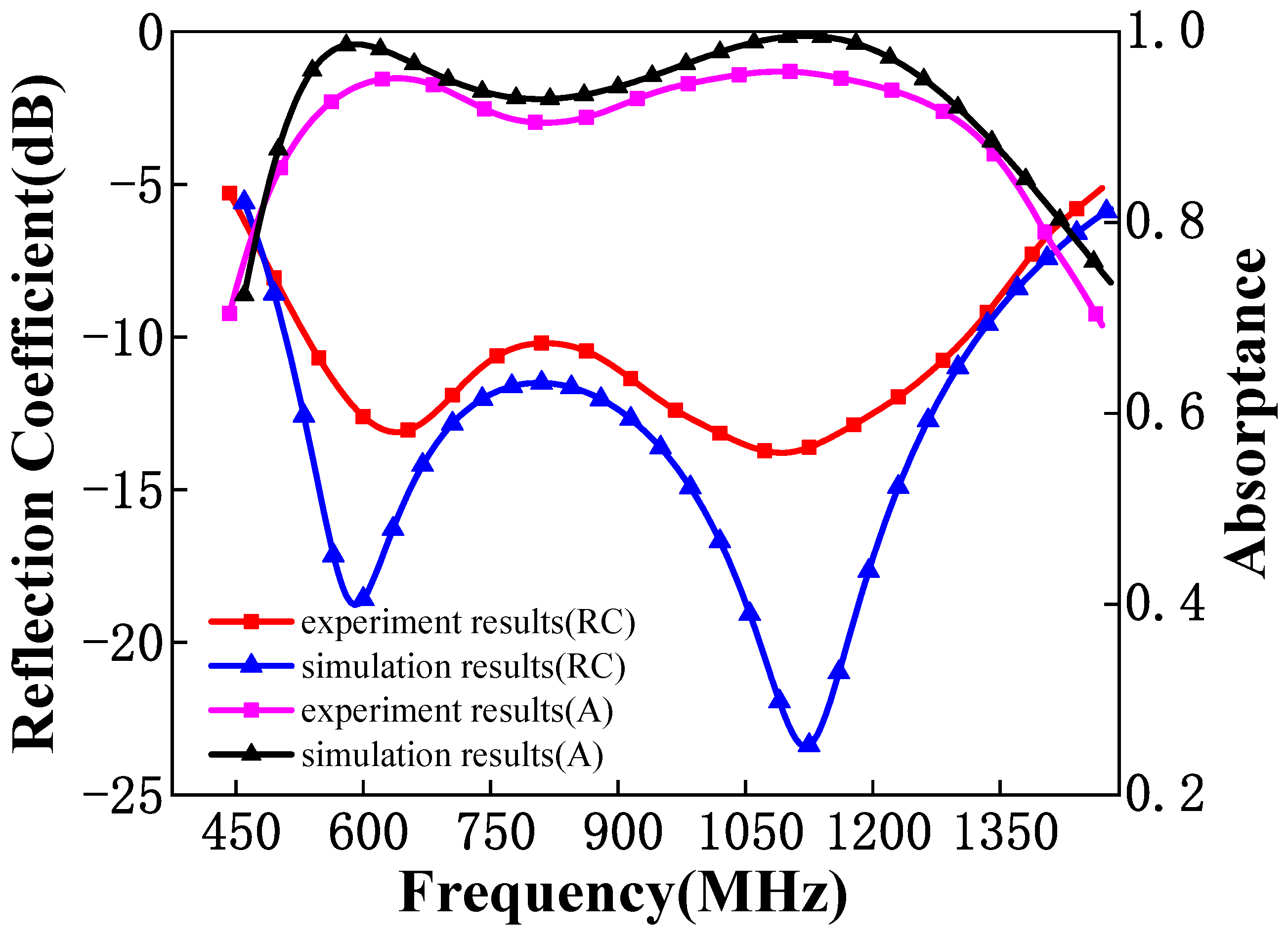
Calibrate the environment with a metal aluminum plate of the same scale, and the difference between it and the fabricated MA is the true reflection coefficient of the sample. As shown in Figure 10, the measured reflection coefficient less than −10 dB under normal incidence is from 535 MHz to 1310 MHz. Compared with simulation results, it can be seen that the bandwidth and the position of the FL and FH in experimental results are basically accurate. However, the absorptance of the experiment results is generally lower. It is because the copper adsorbed on the surface of the through-hole during fabrication is not uniform enough, which leads to the poor conduction effect of some circuits, thus causing errors during the experiment.
5. Conclusions
In this paper, a miniaturized structure of a low-frequency broadband MA was proposed. The structure connects the upper and lower surface circuits of the double-layer dielectric layer through metal holes. The size of the unit cell is 23.8 × 23.8 mm2, realizing the miniaturization of the MA. The absorption band of the MA is from 0.50 GHz to 1.33 GHz, and the unit cell forms two absorption peaks at FL and FH and the corresponding absorptance is 98.9% and 99.5%, respectively. With the help of the simplified equivalent circuit model, the study further analyzed the generation of double absorption peaks and physically validated the sample by the free space method. Table 1 compares the performance of the MA with other related research results. It can be seen that although the structure proposed in reference [9] achieves a larger absorption bandwidth, our work achieves absorption at a lower frequency band and successfully reduces the low-frequency response by 300 MHz, which is extremely challenging in the UHF band. Therefore, the proposed MA combines the advantages of low-frequency, miniaturization and broadband. It is expected to be widely used in the field of UHF stealth technology.
Author Contributions
Conceptualization, W.R., Z.X. and W.L.; methodology, P.W.; software, P.W.; validation, P.W.; formal analysis, W.R., Z.X., W.L. and P.W.; investigation, W.R. and Z.X.; resources, W.L.; data curation, W.L.; writing—original draft preparation, P.W.; writing—review and editing, P.W. and W.R.; visualization, P.W. and W.R.; supervision, W.R.; project administration, W.R. All authors have read and agreed to the published version of the manuscript.
Funding
This research received no external funding.
Data Availability Statement
The data used in this study are available on request from the corresponding author. The data can be easily reproduced from the theoretical analysis described in this study.
Conflicts of Interest
The authors declare no conflict of interest.
References
- Landy, N.I.; Sajuyigbe, S.; Mock, J.J.; Smith, D.R.; Padilla, W.J. Perfect metamaterial absorber. Phys. Rev. Lett. 2008, 100, 207402. [Google Scholar] [CrossRef] [PubMed]
- Yoo, M.; Kim, H.K.; Lim, S. Angular- and Polarization-Insensitive Metamaterial Absorber Using Subwavelength Unit Cell in Multilayer Technology. IEEE Antennas Wirel. Propag. Lett. 2016, 15, 414–417. [Google Scholar] [CrossRef]
- Wu, T.; Ma, Y.-M.; Chen, J.; Wang, L.-L. Triple-band polarization-insensitive metamaterial absorber with low profile. Int. J. RF Microw. Comput.-Aided Eng. 2020, 30, e22314. [Google Scholar] [CrossRef]
- Yoo, M.; Lim, S. Polarization-Independent and Ultrawideband Metamaterial Absorber Using a Hexagonal Artificial Impedance Surface and a Resistor-Capacitor Layer. IEEE Trans. Antennas Propag. 2014, 62, 2652–2658. [Google Scholar]
- Khuyen, B.X.; Tung, B.S.; Yoo, Y.J.; Kim, Y.J.; Kim, K.W.; Chen, L.Y.; Lam, V.D.; Lee, Y. Miniaturization for ultrathin metamaterial perfect absorber in the VHF band. Sci. Rep. 2017, 7, 45151. [Google Scholar] [CrossRef] [PubMed] [Green Version]
- Khuyen, B.X.; Tung, B.S.; Kim, Y.J.; Hwang, J.S.; Kim, K.W.; Rhee, J.Y.; Lam, V.D.; Kim, Y.H.; Lee, Y. Ultra-subwavelength thickness for dual/triple-band metamaterial absorber at very low frequency. Sci. Rep. 2018, 8, 11632. [Google Scholar] [CrossRef] [PubMed] [Green Version]
- Jeong, H.; Nguyen, T.T.; Lim, S. Subwavelength Metamaterial Unit Cell for Low-Frequency Electromagnetic Absorber Applications. Sci. Rep. 2018, 8, 16774. [Google Scholar] [CrossRef] [PubMed]
- Bui, S.T.; Yoo, Y.; Kim, K.W.; Vu, D.L.; Lee, Y. Small-size metamaterial perfect absorber operating at low frequency. Adv. Nat. Sci. Nanosci. Nanotechnol. 2014, 5, 045008. [Google Scholar]
- Araneo, R.; Lovat, G.; Celozzi, S. Compact electromagnetic absorbers for frequencies below 1 GHz. Prog. Electromagn. Res. 2013, 143, 67–86. [Google Scholar] [CrossRef] [Green Version]
- Zuo, W.; Yang, Y.; He, X.; Zhan, D.; Zhang, Q. A Miniaturized Metamaterial Absorber for Ultrahigh-Frequency RFID System. IEEE Antennas Wirel. Propag. Lett. 2016, 16, 329–332. [Google Scholar] [CrossRef]
- Zuo, W.; Yang, Y.; He, X.; Mao, C.; Liu, T. An Ultra-Wideband Miniaturized Metamaterial Absorber in the Ultrahigh-frequency Range. IEEE Antennas Wirel. Propag. Lett. 2017, 16, 928–931. [Google Scholar] [CrossRef]
- Li, W.; Wu, T.; Wang, W.; Guan, J.; Zhai, P. Integrating non-planar metamaterials with magnetic absorbing materials to yield ultra-broadband microwave hybrid absorbers. Appl. Phys. Lett. 2014, 104, 1189. [Google Scholar] [CrossRef] [Green Version]
- Lim, D.; Yu, S.; Lim, S. Miniaturized Metamaterial Absorber Using Three-Dimensional Printed Stair-Like Jerusalem Cross. IEEE Access 2018, 6, 43654–43659. [Google Scholar] [CrossRef]
- Yu, Y.M.; Chiu, C.N.; Chiou, Y.P.; Wu, T.L. A Novel 2.5-Dimensional Ultraminiaturized-Element Frequency Selective Surface. IEEE Trans. Antennas Propag. 2014, 62, 3657–3663. [Google Scholar] [CrossRef]
- Shi, Y.; Tang, W.; Zhuang, W.; Wang, C. Miniaturised frequency selective surface based on 2.5-dimensional closed loop. Electron. Lett. 2014, 50, 1656–1658. [Google Scholar] [CrossRef]
- Yu, Y.M.; Chiu, C.N.; Chiou, Y.P.; Wu, T.L. An Effective Via-Based Frequency Adjustment and Minimization Methodology for Single-Layered Frequency-Selective Surfaces. IEEE Trans. Antennas Propag. 2015, 63, 1641–1649. [Google Scholar] [CrossRef]
- Hussain, T.; Cao, Q.; Kayani, J.K.; Majid, I. Miniaturization of Frequency Selective Surfaces Using 2.5-D Knitted Structures: Design and Synthesis. IEEE Trans. Antennas Propag. 2017, 65, 2405–2412. [Google Scholar] [CrossRef]
- Banadaki, M.D.; Heidari, A.A.; Nakhkash, M. A Metamaterial Absorber with a New Compact Unit Cell. IEEE Antennas Wirel. Propag. Lett. 2017, 17, 205–208. [Google Scholar] [CrossRef]
- Li, Q.; Dong, J.; Li, T.; Cao, X. Broadband Fractal Tree Metamaterial Absorber for P and L Bands Applications. In Proceedings of the 2020 IEEE 3rd International Conference on Electronic Information and Communication Technology (ICEICT), Shenzhen, China, 13–15 November 2020. [Google Scholar]
Figure 1.
Geometry of 2.5D absorber unit cell: (a) multi-layer structure, (b) Metal-Layer Ⅰ and Metal-Layer Ⅲ, (c) Metal-Layer Ⅱ, (d) perspective view, (e) side view and (f) top view.
Figure 1.
Geometry of 2.5D absorber unit cell: (a) multi-layer structure, (b) Metal-Layer Ⅰ and Metal-Layer Ⅲ, (c) Metal-Layer Ⅱ, (d) perspective view, (e) side view and (f) top view.

Figure 2.
The reflection coefficient and absorptance of MA in TE and TM modes.

Figure 3.
Schematic diagram of the arrayed MAs: (a) array distribution and (b) top view.

Figure 4.
The reflection coefficient and absorptance of the arrayed MAs in TE and TM modes.

Figure 5.
Reflection coefficient for oblique incident: (a) TE mode and (b) TM mode.

Figure 6.
Simplified equivalent circuit model based on transmission-line theory.

Figure 7.
Comparison of reflection coefficients between circuit simulation and full-wave simulation.
Figure 7.
Comparison of reflection coefficients between circuit simulation and full-wave simulation.

Figure 8.
Input admittance obtained from the equivalent circuit: (a) imaginary parts of Yd, YLP and Yin, and (b) real part of YLP.
Figure 8.
Input admittance obtained from the equivalent circuit: (a) imaginary parts of Yd, YLP and Yin, and (b) real part of YLP.

Figure 9.
Fabricated absorber and measurement environment: (a) top view of the prototype, (b) side view of the prototype, (c) complete view of the prototype and (d) experimental setup in the anechoic chamber.
Figure 9.
Fabricated absorber and measurement environment: (a) top view of the prototype, (b) side view of the prototype, (c) complete view of the prototype and (d) experimental setup in the anechoic chamber.

Figure 10.
Comparison of reflection coefficients between simulation results and experiment results.


Table 1.
Comparison of the proposed MA with few published MAs.
| Ref. | MA Unit Structure | MA Unit Performance | |||||
|---|---|---|---|---|---|---|---|
| Design Dimension | Lumped Element | Bending Wires | Absorption Band | Relative Bandwidth | Unit Size | Profile Height | |
| [5] | 2.5D | Yes (C) | No | 102 MHz | / | 0.012 λL × 0.012 λL | 0.001 λL |
| [7] | 2D | Yes (L) | No | 2400 MHz | / | 0.027 λL × 0.027 λL | 0.043 λL |
| [8] | 2D | No | Yes | 377 MHz | / | 0.056 λL × 0.045 λL | 0.014 λL |
| [9] | 2D | No | Yes | 395 MHz | / | 0.014 λL × 0.014 λL | 0.011 λL |
| [10] | 2D | Yes (R) | Yes | 840–990 MHz | 16.3% | 0.056 λL × 0.056 λL | 0.060 λL |
| [11] | 2D | Yes (R) | Yes | 800–2700 MHz | 108.5% | 0.053 λL × 0.053 λL | 0.071 λL |
| [18] | 2D | Yes (R) | Yes | 1350–3500 MHz | 88.7% | 0.090 λL × 0.090 λL | 0.097 λL |
| [19] | 2.5D | Yes (R) | No | 1100–2000 MHz | 58.1% | 0.257 λL × 0.257 λL | 0.088 λL |
| our work | 2.5D | Yes (R) | Yes | 500–1330 MHz | 90.7% | 0.040 λL × 0.040 λL | 0.075 λL |
λL is the wavelength corresponding to the lowest frequency. C stands for capacitor, L stands for inductor and R stands for resistor.
Publisher’s Note: MDPI stays neutral with regard to jurisdictional claims in published maps and institutional affiliations. |
© 2022 by the authors. Licensee MDPI, Basel, Switzerland. This article is an open access article distributed under the terms and conditions of the Creative Commons Attribution (CC BY) license (https://creativecommons.org/licenses/by/4.0/).
Share and Cite
MDPI and ACS Style
Wang, P.; Ren, W.; Xue, Z.; Li, W. Design of 2.5D Miniaturized Broadband Absorber for Ultrahigh-Frequency Band. Electronics 2022, 11, 1664. https://0-doi-org.brum.beds.ac.uk/10.3390/electronics11101664
AMA Style
Wang P, Ren W, Xue Z, Li W. Design of 2.5D Miniaturized Broadband Absorber for Ultrahigh-Frequency Band. Electronics. 2022; 11(10):1664. https://0-doi-org.brum.beds.ac.uk/10.3390/electronics11101664
Chicago/Turabian StyleWang, Peipei, Wu Ren, Zhenghui Xue, and Weiming Li. 2022. "Design of 2.5D Miniaturized Broadband Absorber for Ultrahigh-Frequency Band" Electronics 11, no. 10: 1664. https://0-doi-org.brum.beds.ac.uk/10.3390/electronics11101664
Note that from the first issue of 2016, this journal uses article numbers instead of page numbers. See further details here.