
Klystron-like Cyclotron Amplification of a Transversely Propagating Wave by a Spatially Developed Electron Beam


1
Institute of Applied Physics, Russian Academy of Sciences, 119991 Nizhny Novgorod, Russia
2
Advanced School of General and Applied Physics, National Research University “N. I. Lobachevsky State University of Nizhny Novgorod”, 603950 Nizhny Novgorod, Russia
*
Author to whom correspondence should be addressed.
Electronics 2022, 11(3), 323; https://0-doi-org.brum.beds.ac.uk/10.3390/electronics11030323
Submission received: 28 November 2021
/
Revised: 11 January 2022
/
Accepted: 17 January 2022
/
Published: 20 January 2022
(This article belongs to the Special Issue Theoretical and Experimental Research in High-Power Microwave Electronics)
Abstract
:A klystron-like gyro-amplifier based on the excitation of a wave propagating across a spatially developed (in the transverse direction) electron beam is described within the simplest 2-D model. Such a configuration is attractive as a way of implementation of a short-wavelength source with a relatively high level of output power and with the possibility of quasicontinuous frequency tuning. We study the peculiarities of the 2-D process (developing in both the axial and transverse directions) of electron bunching and “free” wave emission from the electron beam in the open drift space, as well as the excitation of the output cavity used to provide formation of a compact and powerful output wave signal. The main problem of this 2-D process is that different fractions of the electron beam (located at different points of its cross-section) move in different wave fields. In addition, excitation of the parasitic wave propagating in the opposite direction relative to the operating wave is possible. However, we show that it is possible to organize effective electron–wave energy exchange for almost all fractions of the electron beam.
1. Introduction
Electron cyclotron masers (including gyrotrons) are the most powerful sources of coherent radiation at sub-terahertz frequencies [1,2,3,4,5]. Currently, such sources, when operating in the sub-terahertz frequency range (that is, at frequencies from 0.3 to 1 THz), are capable of generating power at the levels of 102–103 watts in the continuous generation regime and up to 105 watts in relatively long (microseconds and longer) pulsed regimes. In addition, selective operation at higher cyclotron harmonics is also possible [5]. At the same time, however, the advance of such masers to either higher frequencies or (at the same frequencies) higher levels of the output power aggravates the problem of mode competition inside the operating electrodynamic system. This is especially true for gyro-amplifiers (cyclotron masers operating in the small input signal amplification regime) operated in the sub-terahertz frequency range. In the traditional traveling-wave tube (gyro-TWT) schemes that ensure relatively wide-band frequency tuning, the presence of an extended and oversized electrodynamic system entails the risk of excitation of parasitic near-cutoff modes with high diffraction Q-factors [6,7,8,9,10,11,12,13,14,15]. As a result, the most advanced varieties of gyro-TWTs use low-mode circuits (with their diameters being close to the wavelength) and operate at the frequencies below 100 GHz [7,8,9,12,13,14,15], and even in this case, special selective elements need to be used to provide the stable single-mode operation. We can mention here dielectric and ceramic loss elements [8,9], a periodic dielectric loaded circuit [13], a distributed wall loss configuration of the electrodynamic system [14], and the use of helically corrugated waveguides as a way to provide selective excitation of the second cyclotron harmonic [12,15]. Naturally, the transition to the higher-mode (nearly quasioptical) gyro-TWTs requires the use of even more complicated microwave systems [10,11]. The problem of parasitic oscillations can be avoided by using klystron-type amplifiers with short high-Q operating cavities and a long region of the passive drift of the particles (with no interaction with the wave) [16,17,18,19,20,21,22,23,24,25]. However, in such a scheme of the gyro-amplifier, there are serious limitations imposed on the frequency tuning band, despite the use of low operating modes even in relatively short-wave devices [22,23]. This is especially true for the klystrons with multicavity bunching systems [16,17,18], as well as for the klystrons based on the excitation of higher cyclotron harmonics in the regimes of frequency duplication [19,20] and multiplication [24,25].
In this work, we consider a scheme that combines the advantages of both the TWT and the klystron. In addition, this scheme assumes the use of a spatially developed electron beam, whose transverse dimensions are sufficiently large on the scale of the operating wavelength, which is attractive from the viewpoint of implementation of short-wave high-power radiation sources. We study the cyclotron interaction of a wide electron beam with a wave propagating in vacuum across the direction of the translational motion of electrons. The theory being developed is directly related to the gyro-TWT with the “zigzag” quasioptical system, whose prospects and advantages are more clearly outlined in [26]. However, as shown in this paper, on the basis of the quasioptical electrodynamic geometry described in [26], another scheme of an electronic source of short-wave radiation can be proposed, which may also have an independent value.
The main feature of the described scheme is that the direction of the translational motion of the electrons is perpendicular to the direction of the energy transfer (and, accordingly, the amplification) of the wave. The initial signal in such an amplifier is produced by a modulation of the electron beam in the field of a sufficiently narrow wave signal. In the drift space, the electron beam continues to generate and amplify the wave field, which is carried away from the beam region (in the transverse direction). The process of transverse amplification accelerates the electron bunching process and, at the same time, makes the particle bunching inhomogeneous in the transverse direction. However, if the transverse size of the electron beam is large enough, it turns out that the optima of the grouping of electrons located at different points of the beam cross-section are situated approximately in the same region of the longitudinal coordinate, which leads to the formation of a relatively narrow and powerful wave pulse radiated by the beam in the transverse direction. The transverse organization of the bunching in the electron beam, which leads to synchronization of the radiation maxima of different electrons, can also be ensured in the scheme, where a short quasioptical resonator with a wide frequency band is excited by the electron beam. In this work, we describe a quasianalytical theory of such a gyro-amplifier and present some estimations for a gyro-amplifier with a 60 keV electron beam operating in the sub- terahertz frequency range.
The paper is organized as follows: In Section 2 we describe the 2-D model of the electron–wave interaction used in this paper. Section 3 is devoted to the description of the process of electron bunching (which is accompanied by the radiation of a wave in the transverse direction) in the drift section. Finally, in Section 4 we describe the excitation of a relatively short high-Q output cavity by a beam with a spatially developed structure of the electron bunching.
2. Model and Equations
2.1. The 2-D System of the Electron–Wave Interaction
We consider the cyclotron emission from a beam of electrons moving along the axial magnetic field (Figure 1). This is a spatially developed electron beam, whose transverse dimensions and (Figure 1a) are sufficiently large on the scale of the wavelength of the radiated wave. Along with the translational motion along the z-axis, the particles also perform gyro-oscillations in the x–y plane (Figure 1b), and they interact with a plane wave propagating in the positive direction of the x-axis (Figure 1a,b),
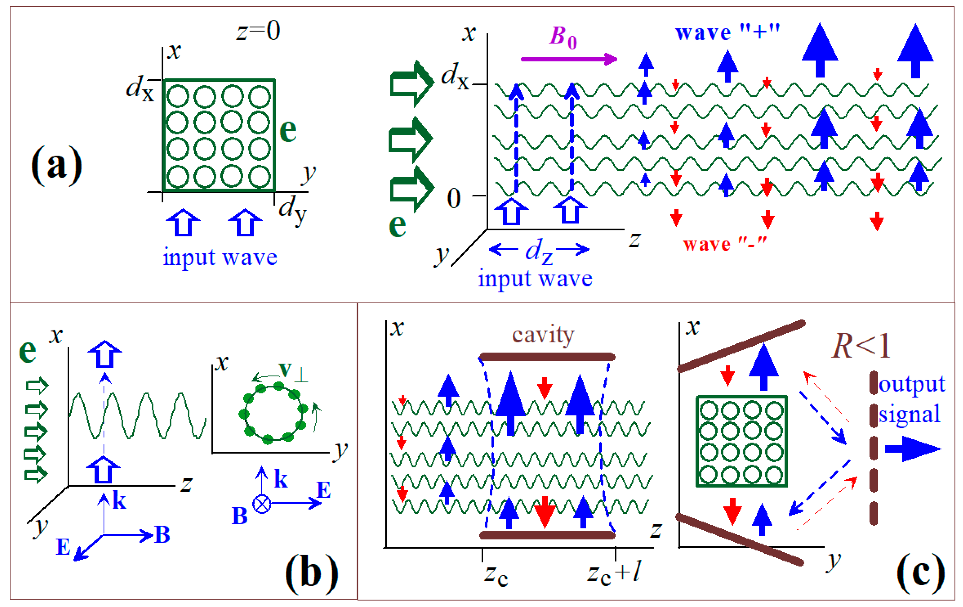
Correspondingly, the electrons possess both the axial velocities, , and the transverse velocities of their gyro-rotation in the magnetic field (Figure 1b),
Here, is the gyro-rotation phase, is the nonrelativistic cyclotron frequency, and is the relativistic Lorentz factor of electrons.
Within the simplest 2-D model of the electron–wave interaction system, we consider a sheet electron beam consisting of electrons with different transverse coordinates x and different initial phases of gyro-rotation. We assume that the fundamental–harmonic cyclotron resonance condition is ensured, . The start of generation of the operating “+” wave is ensured by an input seed signal (a relatively narrow, point-like wave beam) passing through the electron beam at the point z = 0 and providing the initial modulation of the electron energies (Figure 1a). In fact, this seed wave beam plays the role of an input resonator in the traditional klystron scheme.
In principle, bunching of electrons in the field of the operating “+” wave can lead also to emission of the “−” wave possessing the same frequency but propagating in the negative direction of the x-axis (Figure 1a),
This wave should be considered as a parasitic one, as it does not participate in the formation of the output signal.
Next, we will consider the processes of modulation of electron energies by a seed signal and grouping of electrons in the drift space (Figure 1a), as well as excitation by a grouped electron beam of the output cavity (Figure 1c).
In the equation for the evolution of the relativistic electron energy,
we take into account only the resonant, i.e., proportional to ), terms and neglect the terms proportional to ) for both waves:
Here, and are the normalized axial and transverse coordinates, is the change in the relativistic electron energy, are the normalized wave amplitudes, is the electron–wave coupling factor, and is the electron cyclotron phase with respect to the operating “+” wave. In the simplest approximation of a low electron efficiency, , the electron–wave coupling factor can be accepted as constant, and the so-called “forced” term can be neglected in the equation for the electron phase (see, e.g., [27,28,29,30,31]). In this case, this equation takes the following form:
Here, we have taken into account the fact that the axial component of the relativistic momentum, , does not change in the process of interaction of the particle with the transversely propagating waves. In Equation (6), is the mismatch of the electron–wave resonance and is the factor of the electron bunching (here, is the normalized initial axial momentum of electrons).
The initial phases of electrons,
are distributed uniformly over the interval . The presence of the input wave beam leads to modulations of initial electron energies:
In this work, we study two kinds of processes (two stages of the electron–wave interaction) in this system. First, we consider the process of bunching of particles in an open drift space, i.e., one without cavities, as shown in Figure 1a. It is important to mention the difference from the traditional model of the klystron drift space, in which the bunching of particles occurs in the absence of a wave field. Naturally, similarly to the traditional model, the electron bunching factor
which describes the electron source in the wave excitation equations (see Equation (10) further), grows along the axial z-coordinate in the process of the translational motion of electrons along this coordinate. However, an important feature of our system is that the process of electron bunching in the drift region is determined by two factors. Naturally, similarly to the traditional klystron model, the first factor is the initial modulation of electron energies by an input wave signal. However, in the case of a spatially developed electron beam, we should also take into account the process of excitation (and amplification along the transverse x-coordinate) of the operating upstream “+” wave. The field of this wave affects the electron bunching process, and the wave amplitude depends on the transverse x-coordinate. This leads to inhomogeneity of the factor of electron bunching along the transverse coordinate. In addition, in some cases the effect of excitation of the parasitic downstream “−” wave on the transverse inhomogeneity of the electron bunching process can be important.
In order to describe excitations of waves in the open drift space, we use the following simplest equation describing amplification of two waves propagating in the positive and negative directions of the x-axis [27,28,29,30,31]:
The following boundary conditions describe the absence of external signals at the borders of the electron beam:
Here, is the size of the system in the x-direction and .
The wave excitation factor in Equation (10) can be found from the consideration that Equation (5) for the change in the electron energy and Equation (10) for wave excitation must satisfy the law of conservation of energy. The total power of the wave signals leaving the region of the electron beam through its “upper” () and “lower” () boundaries is determined by the following formula:
Here, is the size of the system in the y-direction. This power should be equal to the power of losses of the kinetic energy of electrons,
Here, is the averaged change in the electron Lorentz factors, and I is the total current of the electron beam. On the other hand, the integral
follows from Equations (5) and (10). From Equations (12)–(14) we obtain the following expression for the wave excitation factor:
At the second stage of the electron–wave interaction, a high-Q output cavity is excited by the electron beam bunched in the drift region (Figure 1c). We assume that the operating “+” wave circulates in a quasioptical cavity formed by three mirrors. Note that in such a wave circuit, the operating upstream “+” wave and the parasitic downstream “−” wave stay independent. The latter means that the feedback system is not based on the transformation of the “+” wave into the “−” wave (and vice versa) on the mirrors, as it happens in a two-mirror cavity.
In this model, we use Equations (10) and (11) to describe the excitation of two waves in the drift region. As for the cavity, we assume that it ensures the fixed structure of its eigenwave inside the cavity, and . In this situation, we should use the following substitution in Equation (10):
Here, is the normalized length of the cavity region, and is the axial coordinate of the beginning of the cavity (Figure 1c).
2.2. Normalization of Equations
Further, we use the following normalization:
Here, the transverse coordinate is normalized by the following parameter:
where is the standard Pierce gain parameter [27,28,29,30,31]. In this case, electron motion Equations (5) and (6) are rewritten in the following dimensionless form:
whereas initial conditions (7) and (8) are simplified as follows:
As for wave Equation (10), it is rewritten in the following form:
These equations include two parameters of the system, specifically, its normalized transverse size and the phase incursion of the downstream parasitic wave with respect to the operating wave :
In the case where only the operating upstream “+” wave is taken into account in Equations (18)–(20), the normalized electron efficiency
is related to the normalized power of the upstream wave signal coming out from the system by the following formula:
The generalization of Equation (22) to the case of two waves is obvious. The averaged change in relativistic electron energies is related to the normalized electron efficiency as follows:
Note that the initial energy modulation of the electron beam is determined by the power of the input wave signal. Actually, according to Equation (5),
where is the size of the input wave signal along the z-coordinate (Figure 1a). The power of this signal is determined as
Here, we assume that the size of the input wave signal along the y-coordinate coincides with the corresponding beam size (Figure 1a), such that the whole electron beam interacts with the input signal. Therefore, in the case of the symmetrical input wave beam, , one obtains
Here, , where 17 kA and 500 kV.
3. The Process of Electron Bunching in the Drift Region
3.1. Small-Signal Theory
First, we consider the process of bunching of particles in an open drift space, i.e., without cavities (Figure 1a). At the small-signal stage of this process, we use the single-wave approximation (the parasitic wave is absent, ) and represent the electron phase in the following form:
In this case, the electron bunching factor is expressed as follows:
Then, Equations (18) and (20) transform to the following system:
Here,
and the substitution is used. The initial conditions for Equation (29) have the following form:
Equation (18) leads to the following equation for the function :
It can be easily shown that solutions of Equation (32) should have the following form:
Taking initial conditions (31) into account for and using the Taylor series expansion of the function ,
we obtain the following analytical solution of Equation (32):
Then, the corresponding solution for the 2-D distribution of the amplitude of the operating wave is
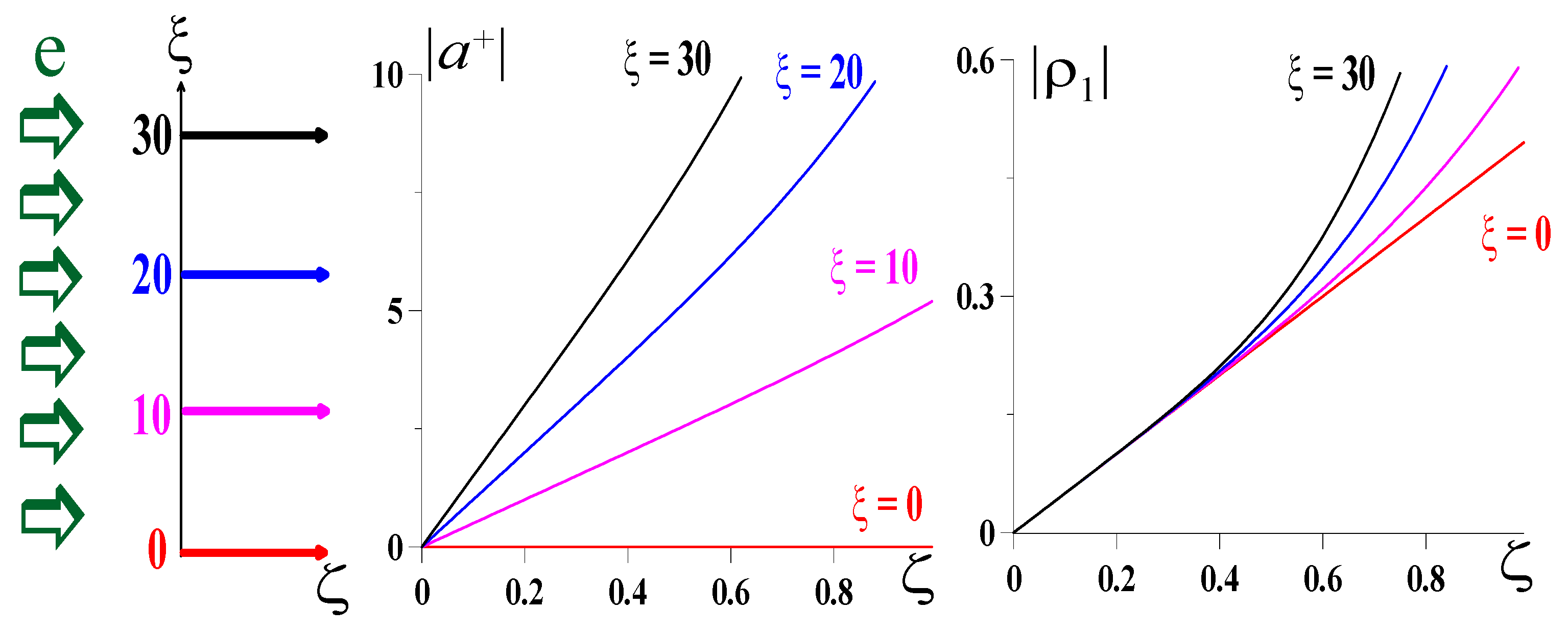
Figure 2 illustrates the results of the small-signal theory, specifically, distributions of the electron bunching factors and the wave amplitudes along the axial coordinate, , for layers of the electron beam with different transverse coordinates . We see that if the normalized transverse size of the beam is not too large , then in all layers of the beam, , the electron bunching factors grow obeying approximately the same law, , and reach the nonlinear saturation level almost at the same points of the axial axis, . Note that the electrons of the lowest layer move in the zero wave field, whereas the wave field acting on the electrons of this layer also increases with the growth of the transverse coordinate of the layer, (Figure 2). This means that in this range of parameters, the main factor determining the bunching of particles is still the initial modulation of the electron energies, while the influence of the wave field is small.
From the point of view of Equation (35), the situation described above corresponds to the fact that only the zero term is important in this series. Considering the next () term of the series leads to the following formula:
Therefore, the transverse inhomogeneity of the electron grouping, which is determined by the wave amplification along the transverse coordinate, becomes noticeable only at the relatively large values of the normalized electron beam thicknesses (Figure 2).
3.2. The Nonlinear Stage of the Electron–Wave Interaction
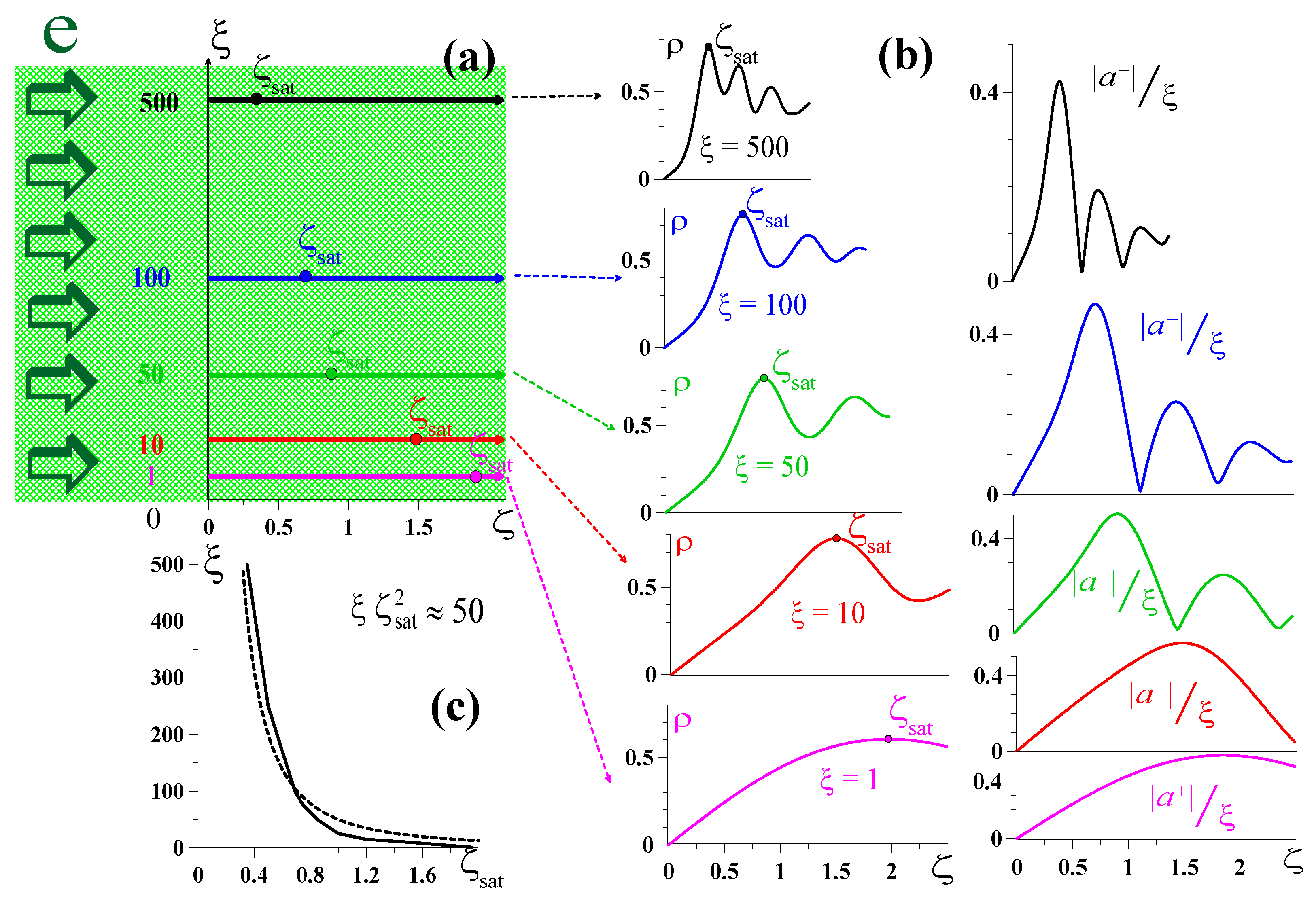
The nonlinear regimes of this system can be studied using the numerical simulations of Equations (18)–(20). Figure 3 illustrates the results of these simulations performed in the single-wave model () for relatively wide electron beams. Note that in this approximation the state of any electron layer of the beam () is determined by the wave emitted from the lower layers (). Therefore, although we consider an electron flow with a width of in the calculations (Figure 3a), any of these layers can be regarded as the upper bound of the electron flow, .
We see that if the normalized width of the beam is relatively small, , then the electron bunching is determined basically by the initial modulation of the electron energy, and the electron bunching factors grow relatively slowly in all layers of the electron flow, such that they reach saturation in the region . If we look at the signal of the operating wave leaving the electron flow from its upper boundary, , we will see that it is extended over the normalized length (Figure 3b, the cases of and 10).
In contrast, if the normalized width of the electron beam becomes large enough (), then most of the electron fractions are bunched almost at the same points of the axial coordinate, . This is due to the fact that the saturated points (the normalized axial coordinates corresponding to the saturation of the electron bunching factors in the electron layer ) become very close to each other for almost all layers of the electron flow. Actually, this can be easily estimated if we add the next terms (with ) to Equation (35):
Therefore, the saturation point of the function is estimated as ; this leads to the following formula (see Figure 3c):
For instance, if , then the saturation points are distributed almost uniformly for all layers of the electrons flow () within the interval (Figure 2), such that . As a result of the calculations, at the upper boundary of the electron flow () we see a wave beam, whose power is spread mainly over a relatively wide segment (Figure 3b). In contrast, in the case of a large normalized width of the electron beam, , the saturation points of 80% of the electron beam layers () are concentrated within a relatively short interval . This leads to the formation of a narrow wave beam leaving the electron flow from its upper boundary.
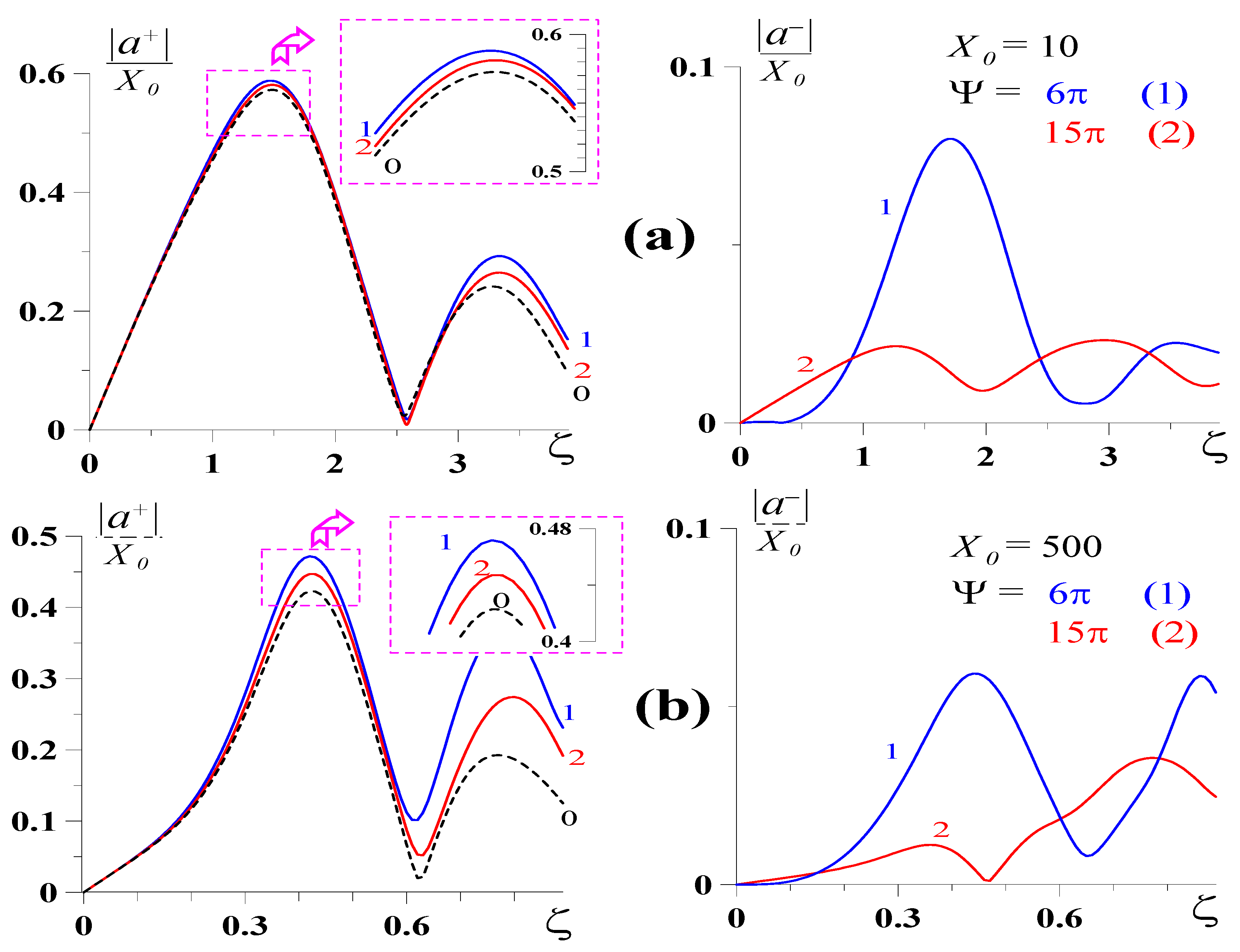
Figure 4 illustrates the effect of the parasitic downstream “−” wave in the cases of electron beams with the normalized widths (Figure 4a) and (Figure 4b). Since the transverse structure of the initial electron bunching is determined by the operating upstream “+” wave, the efficiency of excitation of the “−” wave by such a beam depends on the phase incursion of the parasitic “−” wave with respect to the operating “+” wave. Naturally, if , then both waves are excited by electrons in the same way. The increase in leads to a decrease in the output power of the parasitic “−” wave, as well as to weakening of its effect on the excitation of the “+” wave. Note that the effect of the parasitic downstream “−” wave on the generation of the operating upstream “+” wave is very weak even in the case of relatively small phase incursions (see Figure 4, where corresponds to ). At the same time, the ratio between the peak amplitudes of the downstream and upstream wave beams coming out of the electron beam, , is more than 10% in the case of , whereas in the case of , this ratio decreases down to 3–4%.
4. Excitation of the Output Cavity
According to the results described in Section 3, a large value of the normalized transverse size of the electron beam is required to ensure the concentration of the output signal in a narrow wave beam in the case of the free radiation in the open drift region. This means that in order to form a powerful output wave beam concentrated in a relatively compact spot in the case of relatively small , one should use the regime of excitation of the output cavity by the electron beam bunched in the drift region (Figure 1c). Thus, in order to describe both the electron motion and the excitation of the two waves inside the drift region (, where is the normalized axial coordinate of the beginning of the cavity, see Figure 1c), we use Equations (18)–(20). As for the excitation of two waves inside the cavity (, where L is the normalized length of the cavity), we use the following equations describing the excitation of the cavity eigenmode with the constant structure along the -axis (see Equation (16)):
Evolution of the wave amplitudes inside the cavity in time is described on the basis of the simple trip-by-trip approach, when the input wave amplitude at the (n + 1) wave trip over the cavity (Figure 1c) is determined by the output amplitude of this wave at the previous trip n:
Here, R < 1 is the amplitude feedback coefficient.
4.1. Conditions of Self-Excitation of a Single Cavity
As a first step, we estimate the conditions of self-excitation of the operating output cavity in the case where the input wave signal is absent and, therefore, a nonbunched electron beam enters the cavity. Naturally, such self-excitation should be avoided in the amplifier scheme.
We again use the small-signal approach
for electron motion Equation (18) and wave excitation Equations (40) and (41), and consider these equations in the single-wave approximation, when the parasitic wave is absent, . This leads to the following set of equations:
The following boundary conditions describe the absence of the modulations in the energies and phases of electrons, as well as the presence of a wave signal at the “lower” boundary of the electron beam:
Since in any layer the electrons move in a constant (along the axial z-axis) wave field, one easily obtains
This leads to the following equation of the wave excitation:
Here,
Then, we compare the solution of Equation (43)
with the condition of self-excitations of the cavity,
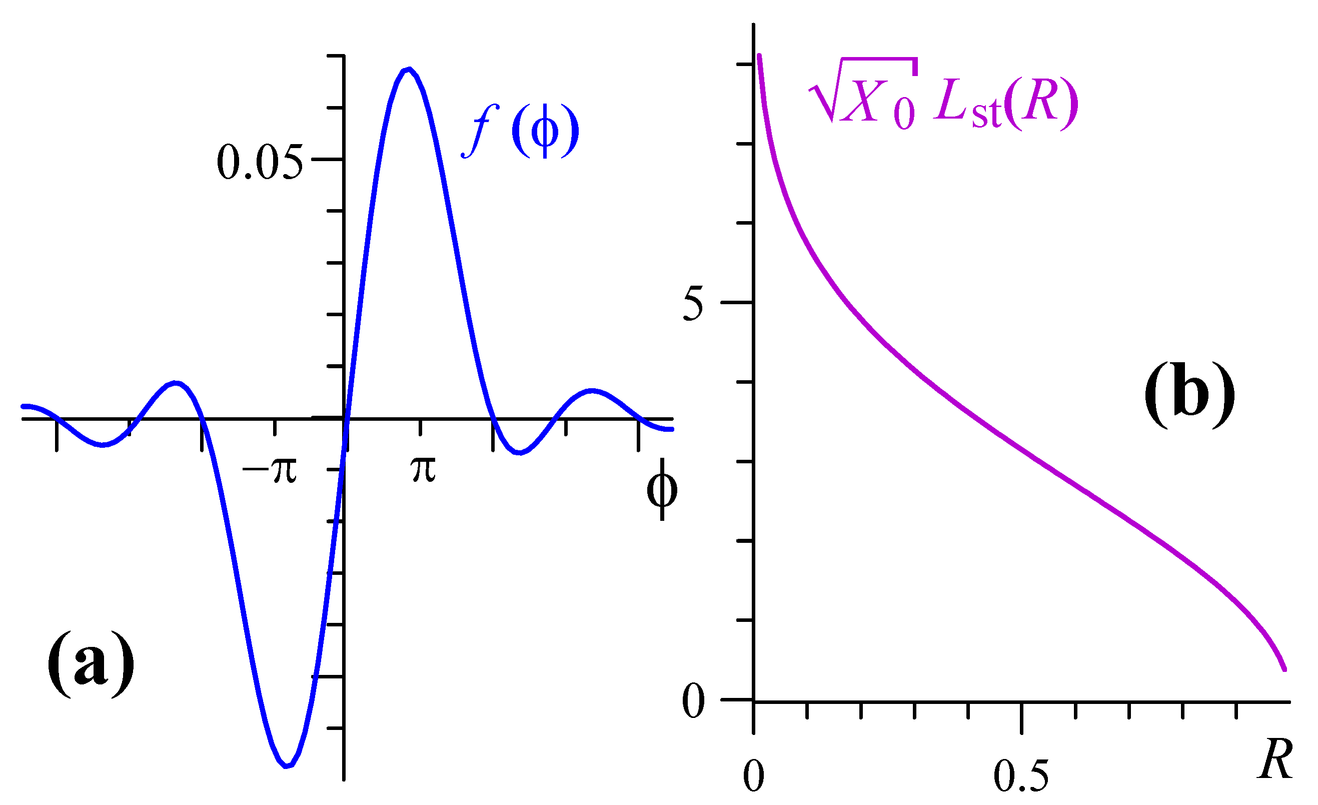
This leads to the following formula describing the threshold of self-excitation of the cavity:
Here, , and
is a derivative of the square of the distribution spectrum (along the longitudinal coordinate) of the wave field inside the cavity. In fact, this is also the normalized efficiency of the electron–wave interactions, which can be found from Equation (18) by finding the second correction (in terms of the wave amplitude ) of the electron energy change averaged over all the initial phases during their passage through the cavity [27,28] in a linear approximation:
4.2. Simulations of the Excitation of the Output Cavity by a Prebunched Electron Beam
In simulations of the nonlinear process of excitation of a high-Q output cavity by a bunched electron beam, we consider the case of a relatively small normalized transverse size of the system, , when the formation of a powerful compact wave beam in the free-radiation drift system is not possible (Figure 3). Figure 6 illustrates optimized klystron-like systems with the output cavity in the case where the amplitude feedback coefficient of the cavity is equal to R = 0.8. The position and the normalized length L of the cavity are optimized to achieve the maximum of the normalized output power coming from the cavity. Here, is the normalized intensity (power density) of the output radiation. This optimization gives the optimal length L = 0.65, which is slightly longer than the normalized length corresponding to the self-excitation of the cavity without the input wave signal (see Figure 5). Therefore, in the simulations, we also study the optimal case for a shorter (L = 0.50) operating cavity, when its self-excitation is impossible.
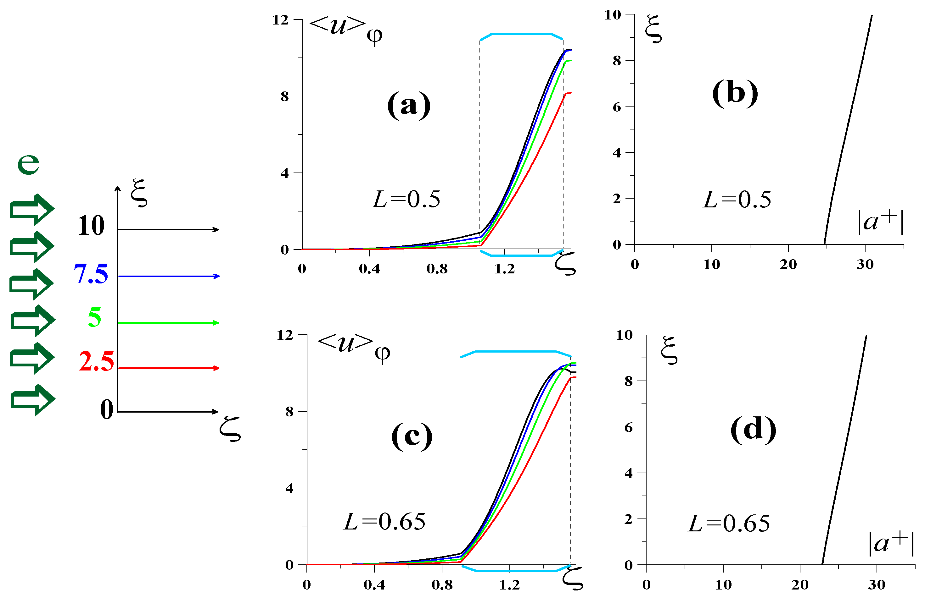
As a first step, we perform simulations in the single-wave model, where the parasitic downstream wave is absent. Figure 6 illustrates averaged changes in the normalized energies of the particles in different transverse layers of the electron beam ( = 2.5, 5, 7.5, and 10) versus the normalized axial coordinate, as well as the structures of the operating wave inside the cavity in the cases of two different normalized lengths of the cavity, L = 0.5 (Figure 6a,b) and 0.65 (Figure 6c,d). These pictures illustrate the situation when the trip-by-trip process described by Equation (41) reaches the stationary stage of the generation,
The use of a high-Q cavity solves the problem described in Section 3, specifically, different dynamics of the electron–wave interaction for different transverse layers of the electron beam. The distribution of the wave amplitude wave over the transverse coordinate is close-to-uniform inside the high-Q cavity (Figure 6b,d). Due to this fact, the normalized efficiencies of the electron–wave interaction are almost the same for all electron fractions (Figure 6a,c). Note that the wave amplitude inside the cavity corresponds to the output wave amplitude . This is significantly higher than the peak amplitude in the regime of the “free” radiation in the drift region without a cavity (see Figure 3).
Figure 7 illustrates the results of the simulations performed within the framework of the two-wave model. Here, we show the calculated distributions over the axial coordinate of the output normalized intensities of the upstream and downstream wave beams, and , coming out from the system at its upper and lower boundaries (in the drift region, R = 0 is assumed). Of the greatest interest is the influence of the presence of the parasitic downstream “−” wave on the generation of the operating upstream “+” wave. In fact, this effect is almost absent even in the case of a relatively small transverse phase size of the beam (recall that corresponds to ). Note that although the parasitic downstream “−” wave is excited inside the cavity, its power is small against the background of the operating upstream “+” wave ( is as small as 0.3–2% in the examples shown in Figure 7a,b).
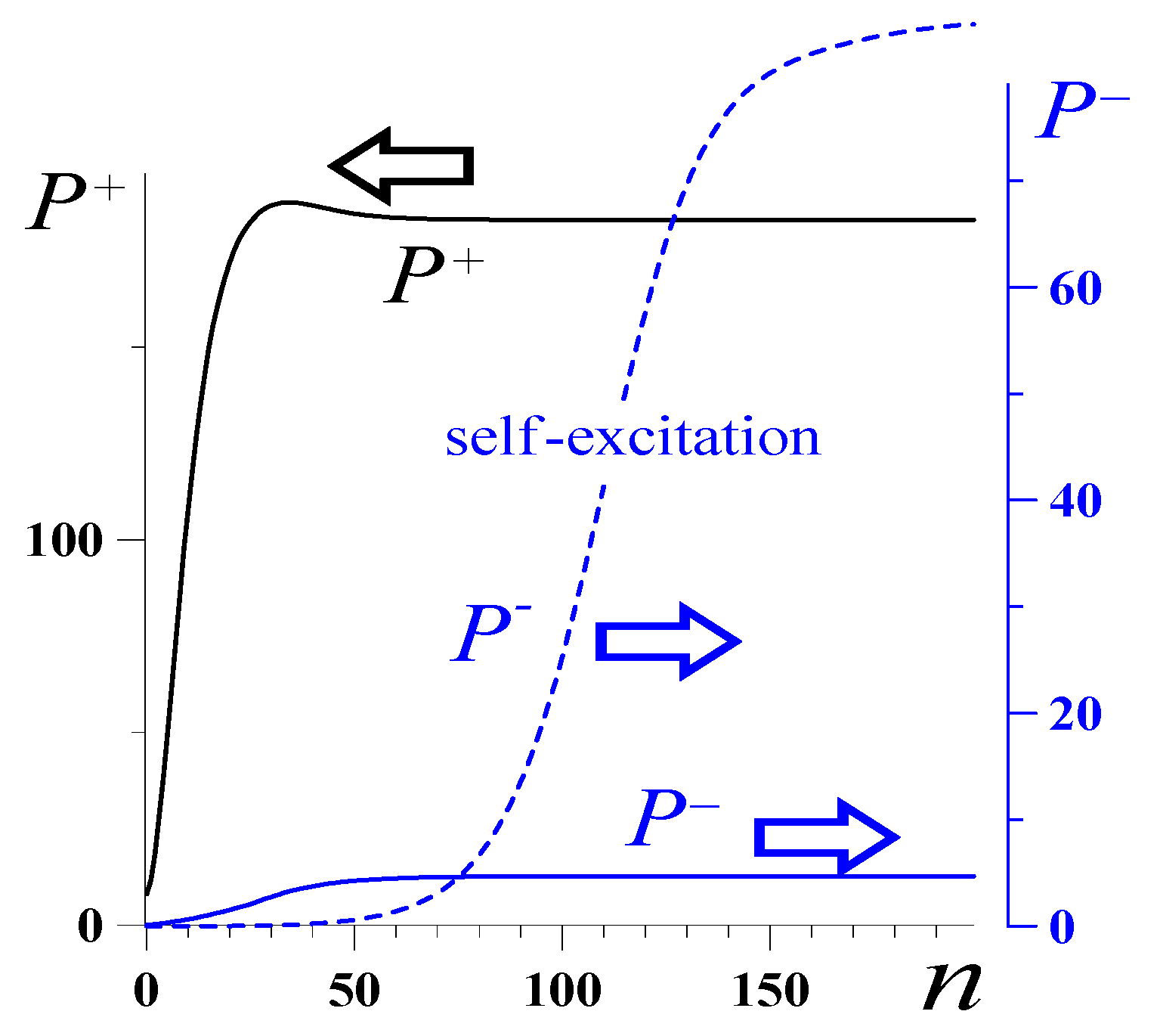
It is important that the latter statement holds even in the case where the cavity length exceeds the threshold of the start of self-excitation of RF oscillations in the cavity without an input signal (Figure 7b). Figure 8 compares the dependences of the normalized output power of the parasitic “downstream” wave on the number of the trip through the cavity, , in the case of self-excitation of this wave without an input signal (calculated within the single-wave model), as well in the case described by Figure 7b, when the electron beam bunched by an input signal excites both the operating upstream “+” wave and the parasitic downstream “−” wave inside the cavity. We see that the presence of the generation of the operating “+” wave excited by the beam with the transverse structure of the electron bunching being proper for this wave leads to significant suppression of the generation of the parasitic “−” wave.
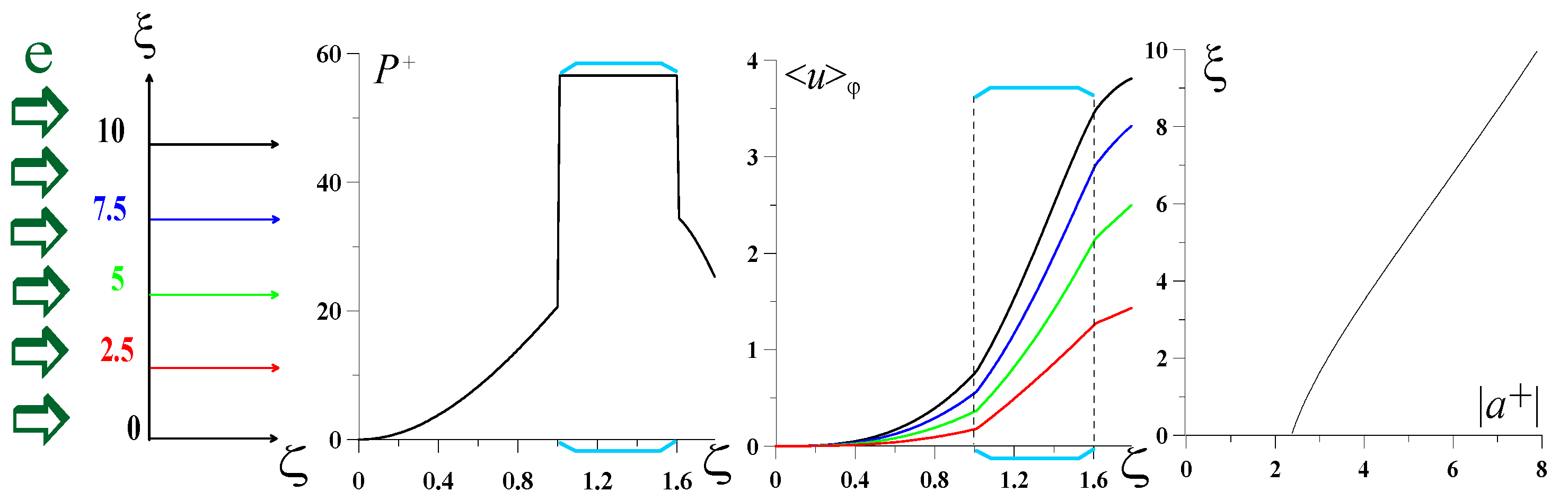
Obviously, self-organization of the electron beam in the transverse direction mentioned above takes place only if one uses a cavity with a high enough Q-factor (the feedback coefficient R) so that the transverse distribution of the wave amplitude is close to uniform, . For the sake of contrast, Figure 9 illustrates the results of the simulations for the optimized klystron-like system in the case of R = 0.3. In this case, we see a significant difference in the normalized efficiencies of electron fractions with different transverse coordinates . As a result, the output power going out from the cavity is significantly lower as compared to the case where R = 0.8.
4.3. Simplest Estimations
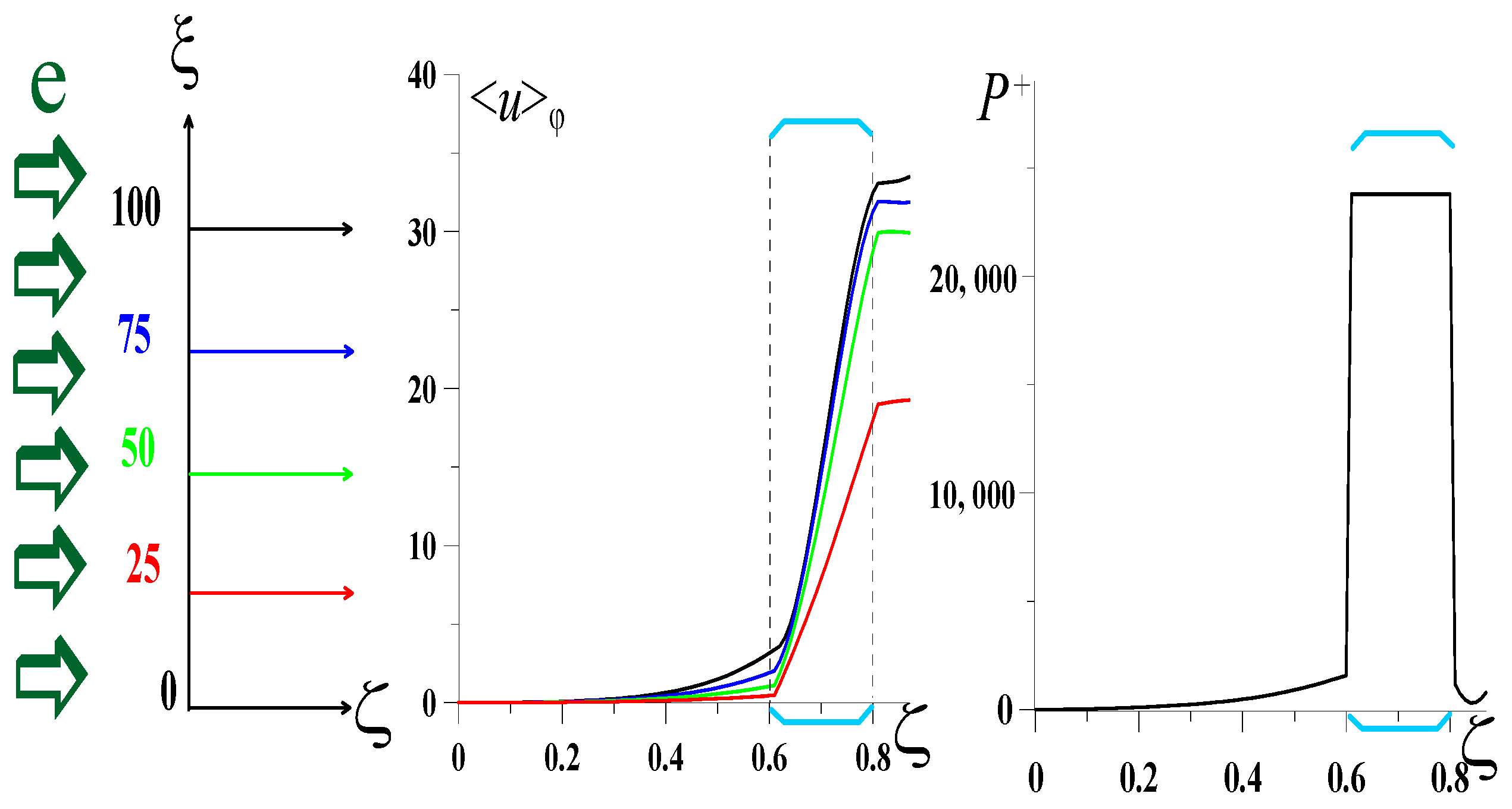
Let us make some estimations for the case of a 60 keV/10A gyrotron beam with the pitch factor of the particles equal to 1.4. For such a beam with the transverse size d ~ 10λ, the Pierce gain factor is , and the bunching factor is . According to Equation (17), the use of a 100 W input wave signal determines that the initial modulation in the electron energy is . In this case, the normalized transverse size of the beam is estimated as . Note that according to Figure 2 and Figure 3, this case differs significantly from the previous case of , because excitation of the transversely propagating wave by the bunching electron beam in the drift region leads to a significant difference in the bunching of the electrons from different transverse layers of the electron beam. Due to this fact, electron fractions with different have different efficiencies inside the operating output cavity. Figure 10 illustrates an optimized system for the case where the normalized transverse size of the system is and the feedback factor of the operating cavity is R = 0.8. We see that the upper half of the electron fractions () have almost the same electron efficiency at the output of the operating cavity. At the same time, the efficiency of particles from the lower layers are considerably lower; for instance, the efficiency of the fraction is about 1.5 times lower than the efficiency of the upper fractions . Nevertheless, an increase by an order of magnitude in the normalized transverse size of the system (from 10 to 100) leads to an increase in the average electron efficiency (for all the measured fractions) also by about an order of magnitude (compare Figure 6 and Figure 10).
The total normalized length of the single-cavity system (Figure 10) corresponds to the actual length , whereas the normalized cavity length corresponds to the actual length . According to Equation (10), the normalized power density of the output radiation together with the normalized cavity length corresponds to the averaged loss in the electron energy and, therefore, to the averaged change in electron energy . This corresponds to the electron efficiency , and the output power is 50 kW. Thus, our simulations show a basic possibility to realize a sub-terahertz gyro-amplifier with an amplification factor close to 30 dB.
5. Discussion
In this paper, we study a scheme of the electron cyclotron maser having a number of advantages. First, the use of a spatially developed electron beam, whose transverse dimensions are sufficiently large on the scale of the operating wavelength, is attractive from the point of view of the implementation of a short-wavelength source with a relatively high level of output power. Second, the use of the free-space system for the electron beam prebunching solves (at least partially) the problem of mode selectivity. Finally, the prebunched electron beam excites a high axial mode (if we talk about the index in the direction of the group velocity) of a quasioptical cavity. Therefore, a quasicontinuous tuning of the frequency can be easily ensured in this system by means of changing the frequency of the input signal and implementing the transition from one mode to another.
The main problem of this system is that the modulation of the electron beam by a quasiplane input (seed) wave beam in open space inevitably leads to the fact that the bunching of electrons in the open drift space is accompanied by the emission of a wave, which is similar to the input wave signal (that is, with the same frequency and wave number), by electrons. Since this wave propagates (and is amplified) in the direction transverse to the electron propagation direction, it turns out that particles of different fractions of the electron beam, which are located at different points of its cross-section, move in the drift space in different wave fields. Therefore, different electron fractions have different degrees of bunching at the entrance to the output cavity. In addition, excitation of the parasitic wave propagating in the opposite direction relative to the operating wave is possible. However, we show in this paper that it is possible to organize effective electron–wave energy exchange for almost all fractions of the electron beam.
Of course, this is done here on the basis of a very simplified model. First of all, the simplified 2-D geometry of the system is used. Second, we use the simplest asymptotic equations of the electron motion and of the electron–wave interaction, and these equations are valid only when the intensity of the electron–wave interaction is weak enough. Next, the simplest equations describing the propagation and amplification of electromagnetic waves in both the drift region and the output cavity are used. In particular, it is assumed that in the cavity region, the transverse structure of the field (relative to the direction of propagation) is fixed by quasioptical mirrors of a high-quality cavity. Such issues as the influence of the quality of the electron beam on the efficiency of the RF source or the possibility of excitation in the drift region of waves directed at an angle to the direction of propagation of the operating and parasitic waves considered in the paper are not discussed. Of course, it is necessary to use much more complex models to simulate specific experimental systems.
At the same time, it seems to us that important assertions can be made already on the basis of the simplest theory given in this paper. As mentioned in the introduction, the scheme considered in this paper is a development of the idea of the “zigzag” gyro-TWT proposed recently [26]. In fact, in this paper we propose another scheme of an electron source of sub-terahertz radiation, which is based on the idea of the “zigzag” quasioptical electrodynamic geometry described in [26], and develop the basic theory of such a device.
Author Contributions
Conceptualization, S.S. and A.S.; methodology, A.S.; validation, E.N. and A.S.; formal analysis, E.N. and A.S.; investigation, E.N. and A.S.; writing—original draft preparation, E.N. and A.S.; writing—review and editing, S.S. and A.S.; project administration, S.S. All authors have read and agreed to the published version of the manuscript.
Funding
This research was funded by the Russian Science Foundation, grant No. 21-19-00443.
Institutional Review Board Statement
Not applicable.
Informed Consent Statement
Not applicable.
Data Availability Statement
Not applicable.
Conflicts of Interest
The authors declare no conflict of interest.
Nomenclature
| Variable | Definition | Formula |
| Axial static magnetic field. | ||
| Electric field of the operating “upstream” wave. | ||
| Electric field of the parasitic “downstream” wave. | ||
| t | Time. | |
| z | Axial coordinate. | |
| Wave frequency. | ||
| Wavelength. | ||
| Wavenumber. | ||
| Components of the electron velocity. | ||
| Complex transverse velocity. | ||
| Gyro-rotation phase of a particle. | ||
| Initial gyro-phase. | ||
| Nonrelativistic electron cyclotron frequency. | ||
| m | Electron mass. | |
| c | Speed of light. | |
| Relativistic electron Lorentz factor. | ||
| Change in the relativistic electron Lorentz factor. | ||
| Normalized z-coordinate. | ||
| Normalized x-coordinate. | ||
| Normalized wave amplitudes. | ||
| Electron–wave coupling factor. | ||
| Electron cyclotron phase with respect to the operating wave “+”. | ||
| Initial phase. | ||
| Amplitude of the initial modulation of electron energies. | ||
| Mismatch of the electron–wave resonance. | ||
| Factor of the electron bunching. | ||
| Normalized initial axial momentum of electrons. | ||
| Electron bunching factor. | ||
| Sizes of the system in the x- and y-directions. | ||
| Normalized size of the system in the x-direction. | ||
| Total power of the wave signals leaving the system through the “upper” and “lower” boundaries. | ||
| Power of losses of the kinetic energy of electrons. | ||
| I | Total current in the electron beam. | |
| Averaged change in the electron Lorentz factors. | ||
| Wave excitation factor. | ||
| Alfven current. | 17 kA | |
| Electron bunching factor averaged inside the cavity. | ||
| Normalized cavity length. | ||
| Axial coordinate of the beginning of the cavity. | ||
| Normalized change in the electron energy. | ||
| Normalized axial coordinate. | ||
| Normalized transverse coordinate. | ||
| Normalized mismatch of the electron–wave resonance. | ||
| Normalized wave amplitudes. | ||
| Parameter of the normalization. | ||
| Pierce gain parameter. | ||
| Normalized transverse size of the system. | ||
| Phase incursion of the parasitic wave “-” with respect to the operating wave “+”. | ||
| Normalized electron efficiency. | ||
| Electric field of the input wave signal. | ||
| Power of the input wave signal. | ||
| Size of the input wave signal along the z-coordinate. | ||
| Power of the normalization. | 8.5 GW | |
| Voltage of the normalization. | 500 kV | |
| Small perturbation of the electron bunching factor. | ||
| Small perturbation of the electron phase. | ||
| R | Amplitude feedback coefficient in the output cavity. | |
| Incursion of the electron phase inside the cavity. | ||
| Output normalized intensity of the “upstream” wave beam. | ||
| Output normalized intensity of the “downstream” wave beam. |
References
- Thumm, M. State-of-the-Art of High-Power Gyro-Devices and Free Electron Masers. J. Infrared Millim. Terahertz Waves 2020, 41, 1–140. [Google Scholar] [CrossRef] [Green Version]
- Litvak, A.G.; Denisov, G.G.; Glyavin, M.Y. Russian gyrotrons: Achievements and trends. IEEE J. Microw. 2021, 1, 260–268. [Google Scholar] [CrossRef]
- Glyavin, M.Y.; Denisov, G.G.; Zapevalov, V.E.; Kuftin, A.N.; Luchinin, A.G.; Manuilov, V.N.; Morozkin, M.V.; Sedov, A.S.; Chirkov, A.V. Terahertz gyrotrons: State of the art and prospects. J. Commun. Technol. Electron. 2014, 59, 792–797. [Google Scholar] [CrossRef]
- Glyavin, M.; Denisov, G. Development of high power THz band gyrotrons and their applications in physical research. In Proceedings of the International Conference on Infrared, Millimeter, and Terahertz Waves, IRMMW-THz, Cancun, Mexico, 27 August–1 September 2017; p. 8067024. [Google Scholar]
- Bandurkin, I.V.; Bratman, V.L.; Kalynov, Y.K.; Osharin, I.V.; Savilov, A.V. Terahertz Large-Orbit High-Harmonic Gyrotrons at IAP RAS: Recent Experiments and New Designs. IEEE Trans. Electron Devices 2018, 65, 2287–2293. [Google Scholar] [CrossRef]
- Gold, S.H.; Kirkpatrick, D.A.; Fliflet, A.W.; McCowan, R.B.; Kinkead, A.K.; Hardesty, D.L.; Sucy, M. High-voltage millimeter-wave gyro-traveling-wave amplifier. J. Appl. Phys. 1991, 69, 6696–6698. [Google Scholar] [CrossRef]
- Chu, K.R.; Chen, H.Y.; Hung, C.L.; Chang, T.H.; Barnett, L.R.; Chen, S.H.; Yang, T.T. Ultrahigh gain gyrotron traveling wave amplifier. Phys. Rev. Lett. 1998, 81, 4760–4763. [Google Scholar] [CrossRef] [Green Version]
- Yan, R.; Luo, Y.; Liu, G.; Pu, Y. Design and experiment of a q-band Gyro-TWT loaded with lossy dielectric. IEEE Trans. Electron Devices 2012, 59, 3612–3617. [Google Scholar] [CrossRef]
- Garven, M.; Calame, J.P.; Danly, B.G.; Nguyen, K.T.; Levush, B.; Wood, F.N.; Pershing, D.E. A gyrotron-traveling-wave tube amplifier experiment with a ceramic loaded interaction region. IEEE Trans. Plasma Sci. 2002, 30, 885–893. [Google Scholar] [CrossRef]
- Sirigiri, J.R.; Shapiro, M.A.; Temkin, R.J. High-power 140-GHz quasioptical gyrotron traveling-wave amplifier. Phys. Rev. Lett. 2003, 90, 2583021–2583024. [Google Scholar] [CrossRef] [Green Version]
- Nanni, E.A.; Lewis, S.M.; Shapiro, M.A.; Griffin, R.G.; Temkin, R.J. Photonic-band-gap traveling-wave gyrotron amplifier. Phys. Rev. Lett. 2013, 111, 235101. [Google Scholar] [CrossRef] [Green Version]
- Denisov, G.G.; Bratman, V.L.; Cross, A.W.; He, W.; Phelps, A.D.R.; Ronald, K.; Samsonov, S.V.; Whyte, C.G. Gyrotron traveling wave amplifier with a helical interaction waveguide. Phys. Rev. Lett. 1998, 81, 5680–5683. [Google Scholar] [CrossRef]
- Zeng, X.; Du, C.; Li, A.; Gao, S.; Wang, Z.; Zhang, Y.; Zi, Z.; Feng, J. Design and preliminary experiment of w-band broadband te02 mode gyro-twt. Electronics 2021, 10, 1950. [Google Scholar] [CrossRef]
- Song, H.H.; McDermott, D.B.; Hirata, Y.; Barnett, L.R.; Domier, C.W.; Hsu, H.L.; Chang, T.H.; Tsai, W.C.; Chu, K.R.; Luhmann, N.C., Jr. Theory and experiment of a 94 GHz gyrotron traveling-wave amplifier. Phys. Plasmas 2004, 11, 2935–2941. [Google Scholar] [CrossRef] [Green Version]
- Samsonov, S.V.; Bogdashov, A.A.; Denisov, G.G.; Gachev, I.G.; Mishakin, S.V. Cascade of Two W -Band Helical-Waveguide Gyro-TWTs with High Gain and Output Power: Concept and Modeling. IEEE Trans. Electron Devices 2017, 64, 1305–1309. [Google Scholar] [CrossRef]
- Arfin, B.; Ganguly, A.K. Three-cavity gyroklystron amplifier experiment. Int. J. Electron. 1982, 53, 709–714. [Google Scholar] [CrossRef]
- Zasypkin, E.V.; Moiseev, M.A.; Sokolov, E.V.; Yulpatov, V.K. Effect of penultimate cavity position and tuning on three-cavity gyroklystron amplifier performance. Int. J. Electron. 1995, 78, 423–433. [Google Scholar] [CrossRef]
- Furuno, D.S.; McDermott, D.B.; Luhmann, N.C.; Vitello, P.; Ko, K. Operation of a Large-Orbit High-Harmonic Multicavity Gyroklystron Amplifier. IEEE Trans. Plasma Sci. 1988, 16, 155–161. [Google Scholar] [CrossRef]
- Lawson, W.; Matthews, H.W.; Lee, M.K.E.; Calame, J.P.; Hogan, B.; Cheng, J.; Latham, P.E.; Granatstein, V.L.; Reiser, M. High-power operation of a K-band second-harmonic gyroklystron. Phys. Rev. Lett. 1993, 71, 456–459. [Google Scholar] [CrossRef] [PubMed]
- Zasypkin, E.V.; Moiseev, M.A.; Gachev, I.G.; Antakov, I.I. Study of high-power ka-band second-harmonic gyroklystron amplifier. IEEE Trans. Plasma Sci. 1996, 24, 666–670. [Google Scholar] [CrossRef]
- Nusinovich, G.S.; Danly, B.G.; Levush, B. Gain and bandwidth in stagger-tuned gyroklystrons. Phys. Plasmas 1997, 4, 469–478. [Google Scholar] [CrossRef]
- Zasypkin, E.V.; Gachev, I.G.; Antakov, I.I. Experimental study of a W-band Gyroklystron amplifier operated in the high-order TE021 cavity mode. Radiophys. Quantum Electron. 2012, 55, 309–317. [Google Scholar] [CrossRef]
- Nix, L.J.R.; Zhang, L.; He, W.; Donaldson, C.R.; Ronald, K.; Cross, A.W.; Whyte, C.G. Demonstration of efficient beam-wave interaction for a MW-level 48 GHz gyroklystron amplifier. Phys. Plasmas 2020, 27, 05310. [Google Scholar] [CrossRef]
- Savilov, A.V.; Nusinovich, G.S. On the theory of frequency-quadrupling gyroklystrons. Phys. Plasmas 2007, 14, 053113. [Google Scholar] [CrossRef]
- Savilov, A.V.; Nusinovich, G.S. Stability of frequency-multiplying harmonic gyroklystrons. Phys. Plasmas 2008, 15, 013112. [Google Scholar] [CrossRef]
- Samsonov, S.V.; Denisov, G.G.; Bogdashov, A.A.; Gachev, I.G. Cyclotron Resonance Maser with Zigzag Quasi-Optical Transmission Line: Concept and Modeling. IEEE Trans. Electron Dev. 2021, 68, 5846–5850. [Google Scholar] [CrossRef]
- Bratman, V.L.; Ginzburg, N.S.; Petelin, M.I. Common properties of free electron lasers. Opt. Commun. 1979, 30, 409–412. [Google Scholar] [CrossRef]
- Nusinovich, G.S. Introduction to the Physics of Gyrotrons; John Hopkins University Press: Baltimore, MD, USA, 2004. [Google Scholar]
- Glyavin, M.Y.; Oparina, Y.S.; Savilov, A.V.; Sedov, A.S. Optimal parameters of gyrotrons with weak electron-wave interaction. Phys. Plasmas 2016, 23, 093108. [Google Scholar] [CrossRef]
- Savilov, A.V.; Bespalov, P.A.; Ronald, K.; Phelps, A.D.R. Dynamics of excitation of backward waves in long inhomogeneous systems. Phys. Plasmas 2007, 14, 113104. [Google Scholar] [CrossRef]
- Kuzikov, S.V.; Savilov, A.V. Regime of “multi-stage” trapping in electron masers. Phys. Plasmas 2018, 25, 113114. [Google Scholar] [CrossRef]
Figure 1.
The 2-D model of interaction of the electron beam with the operating “+” wave propagating across the spatially developed electron beam. The parasitic backward “−” wave is also shown. (a) The transverse cross-section of the electron beam, the input wave signal, and excitation of the “+” and “−” waves inside the drift region. (b) The translational and transverse rotator motion of electrons against the background of the fields of the operating plane “+” wave. (c) Excitation of the “+” and “−” waves inside a three-mirror cavity.

Figure 2.
Dependences of the wave amplitudes and the electron bunching factors on the normalized axial coordinate found within the small-signal approximation for different transverse layers of the electron beam, .
Figure 2.
Dependences of the wave amplitudes and the electron bunching factors on the normalized axial coordinate found within the small-signal approximation for different transverse layers of the electron beam, .

Figure 3.
(a) Different layers of the electron beam (having different normalized transverse coordinates, ); calculated axial coordinates of the saturation points are also shown. (b) Evolutions of the electron bunching efficiency and the amplitude of the operating wave with the axial coordinate within the single-wave model. (c) Calculated (solid curve) and analytical (dashed curve) relations between the normalized transverse coordinate of the electron layer and the normalized axial coordinate of the saturation points.

Figure 4.
Influence of excitation of the parasitic “−” wave in the cases of different normalized widths of the electron beam, 10 (a) and 500 (b). Distributions of the output signals of the two waves, and , over the axial coordinate, . Curves 0 illustrate the case when the “−” wave is absent; other curves (1 and 2) correspond to the cases of different phase incursions and of the “−” wave.

Figure 5.
(a) Function describing the efficiency of the electron–wave interaction in the small-signal regime. (b) Starting parameters of the cavity versus the reflection coefficient.
Figure 5.
(a) Function describing the efficiency of the electron–wave interaction in the small-signal regime. (b) Starting parameters of the cavity versus the reflection coefficient.

Figure 6.
Excitation of the output cavity by a bunched beam in the single-wave model for the case where the amplitude feedback coefficient of the cavity is R = 0.8. Averaged changes in the normalized energies of the electrons of different transverse layers of the beam ( = 2.5, 5, 7.5, and 10) versus the normalized axial coordinate (a) and the structure of the operating wave inside the cavity (b) in the case of the normalized cavity length L = 0.65. (c,d) The same plots in the case of L = 0.5. Positions of the cavities are also shown in Figure 6a,c.

Figure 7.
Excitation of the output cavity by a bunched beam within the two-wave model. Normalized intensities of the upstream and downstream output wave beams versus the axial coordinate in the whole system, as well as inside the operating cavity in the cases of the normalized cavity lengths L = 0.5 (a) and L = 0.65 (b). Curves 0 illustrate the case when the “−” wave is absent; the other curves (1 and 2) correspond to the cases of different phase incursions and of the “−” wave. Positions of the cavities are also shown.

Figure 8.
Solid curves: simulations of excitation of the output cavity by a bunched beam within the two-wave model in the case where the amplitude feedback coefficient of the cavity is R = 0.8; the normalized intensity (power density) of the output radiation of the operating upstream wave and the parasitic downstream wave versus the number of the wave trips through the cavity. Dashed curve: the normalized intensity of the parasitic downstream wave versus the number of the trips in the regime of self-excitation of this wave in the cavity without an input signal.

Figure 9.
Simulations of excitation of the output cavity by a bunched beam within the single-wave model in the case where the amplitude feedback coefficient of the cavity is R = 0.3. The normalized intensity (power density) of the output radiation versus the normalized axial coordinate, averaged changes in the normalized energies of electrons in different transverse layers of the beam ( = 2.5, 5, 7.5, and 10) versus the normalized axial coordinate, and the structure of the operating wave inside the cavity.

Figure 10.
Simulations of the excitation of the output cavity by a bunched beam within the single-wave model in the case where the amplitude feedback coefficient of the cavity is R = 0.8 and the normalized transverse size of the system is . Averaged changes in the normalized energies of the electrons in different transverse layers of the beam ( = 25, 50, 75, and 100) versus the normalized axial coordinate, and the normalized intensity (power density) of the output radiation versus the normalized axial coordinate. Position of the cavity is also shown.

Publisher’s Note: MDPI stays neutral with regard to jurisdictional claims in published maps and institutional affiliations. |
© 2022 by the authors. Licensee MDPI, Basel, Switzerland. This article is an open access article distributed under the terms and conditions of the Creative Commons Attribution (CC BY) license (https://creativecommons.org/licenses/by/4.0/).
Share and Cite
MDPI and ACS Style
Novak, E.; Samsonov, S.; Savilov, A. Klystron-like Cyclotron Amplification of a Transversely Propagating Wave by a Spatially Developed Electron Beam. Electronics 2022, 11, 323. https://0-doi-org.brum.beds.ac.uk/10.3390/electronics11030323
AMA Style
Novak E, Samsonov S, Savilov A. Klystron-like Cyclotron Amplification of a Transversely Propagating Wave by a Spatially Developed Electron Beam. Electronics. 2022; 11(3):323. https://0-doi-org.brum.beds.ac.uk/10.3390/electronics11030323
Chicago/Turabian StyleNovak, Ekaterina, Sergey Samsonov, and Andrei Savilov. 2022. "Klystron-like Cyclotron Amplification of a Transversely Propagating Wave by a Spatially Developed Electron Beam" Electronics 11, no. 3: 323. https://0-doi-org.brum.beds.ac.uk/10.3390/electronics11030323
Note that from the first issue of 2016, this journal uses article numbers instead of page numbers. See further details here.