
Small Group Delay Variation and High Efficiency 3.1–10.6 GHz CMOS Power Amplifier for UWB Systems


1
Higher Institute of Engineering and Technology, New Minia 11765, Egypt
2
Faculty of Engineering, Minia University, Minia 61519, Egypt
3
Faculty of Engineering, Egyptian–Russian University, Cairo 11829, Egypt
4
National Telecommunications Institute (NTI), Cairo 11768, Egypt
*
Author to whom correspondence should be addressed.
Electronics 2022, 11(3), 328; https://0-doi-org.brum.beds.ac.uk/10.3390/electronics11030328
Submission received: 18 December 2021
/
Revised: 15 January 2022
/
Accepted: 17 January 2022
/
Published: 21 January 2022
(This article belongs to the Special Issue 10th Anniversary of Electronics: Advances in Circuit and Signal Processing)
Abstract
:A two-stage cascaded power amplifier (PA) employing a proposed Resistor-Capacitor (RC) interstage was provided and simulated. The current-reuse topology is employed at the first stage to lower the power consumption, while the RC interstage helps to enrich the gain flatness and the wideband matching. The shunt peaking topology in a common source configuration is adopted at the second stage to enhance the power gain. The postlayout simulation is performed using the TSMC 65 nm CMOS process operating in a frequency band of 3.1 GHz to 10.6 GHz. The postlayout simulation results indicate that a high flat gain of approximately 22.8 ± 1.2 dB, small group delay variation of ±50 ps, and good input and output matching of less than −10 dB are achieved over the desired working band. Moreover, a saturated output power of 10 dBm and maximum power-added efficiency (PAE) of 29.5% is achieved at 6 GHz. The proposed PA consumes the low power of 15.5 mW from 1.2 V supply voltage.
1. Introduction
Ultra-wideband (UWB) systems became more attractive in today’s world owing to their capability to transmit data at a high rate and low power over a broad frequency. UWB systems are commonly used in short-distance wireless local area networks and be suitable for wireless personal area networks (WPAN) applications, sensor networks, and imaging systems [1]. The power amplifier is considered one of the most critical element in the UWB systems for being the major power consumption block among the system blocks. It is responsible for transmitting the RF signal to the required power level to meet the requirements of various applications. The design of the power amplifier needs to provide high power gain with broadband input and output matching, suitable efficiency, good linearity, low power consumption, and low group delay variations within the broad frequency spectrum. Therefore, the power amplifier design requires a better balance between efficiency, linearity, and gain requirement. The CMOS PAs for UWB applications presented in the literature adopt different techniques and operate over different frequency bands [2,3,4,5,6,7,8,9,10,11,12,13,14].
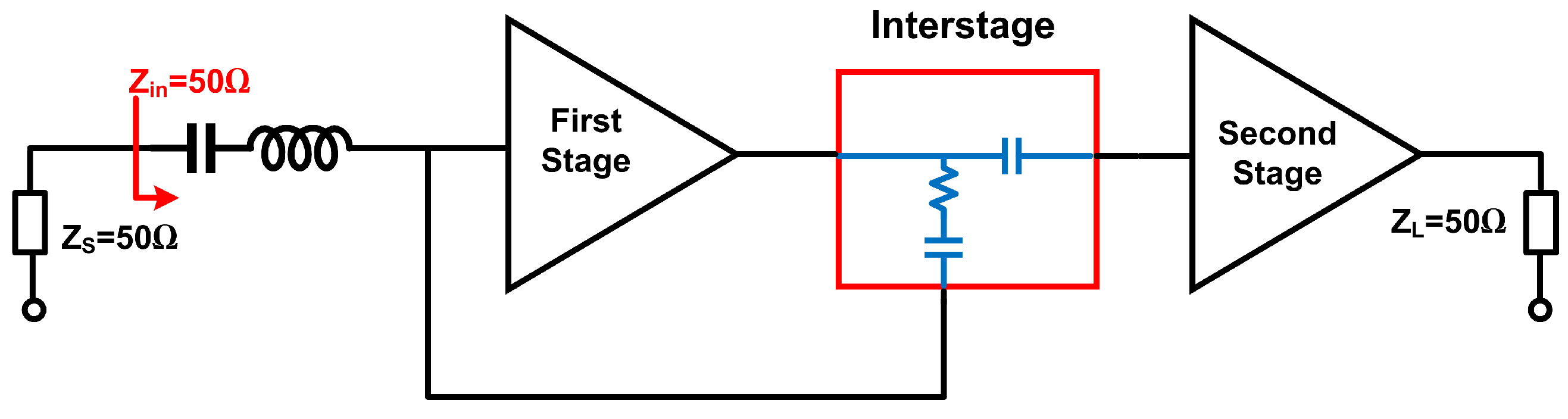
The distributed amplifier (DA) topology provides wideband matching and good gain flatness but consumes more power and a large chip of area based on the distribution of several amplifying stages and transmission line configuration linked between them [2]. However, the DA in [3] achieved not only a high flat gain over the bandwidth (BW) of operation, but also achieved 25 mW low power consumption by employing the technique of tapered transmission line. The resistive shunt feedback topology adopted in [4] attained a flat gain with wide bandwidth and low group delay variation of ±18.3 ps; in addition, it consumed low power of 19 mW. [5] adopted both the active RC feedback for linearity enhancement and bandwidth extension and the double resonance network for flat gain and good broadband matching. The RLC matching topology introduced in [6] offered a wideband matching with low power consumption, but the design provided a low average power gain of 10 dB. [7] adopted the shunt peaking topology for the first and second stages to realize the high flat gain, good linearity, and group delay variation, whereas it adopted the shunt resistive feedback for the first stage for wideband input matching. The inductive degeneration topology demonstrated in [8,9] helped to attain a high flat gain with high power-added efficiency, but the matching was not as impactful as with resistive feedback topology. The common gate amplifier combined with RC-shunt feedback and inductive degeneration was adopted in [10] to realize a good matching with a high flat gain and good linearity. The interstage transformer topology [11] provided broadband linearity and consumed low power, but the gain was limited. Stagger-tuning topology [12] exposed three-stage amplifiers; each stage was tuned to a different frequency for broadband operation and flatten gain, but that caused the consumption of the high power. Current-reuse topology is adopted in the UWB-PA design to attain a low power consumption, better isolation, low group delay, and enhance gain flatness as in [13] but, this topology introduced poor matching and low power gain. [14] improved the broadband matching by employing a common gate amplifier combined with the current reused topology for the input stage. Furthermore, Designing UWB-PA that covers the whole band from 3.1 to 10.6 GHz and satisfies all the ultra-wideband specifications is a challenge. In this paper, a low group-delay variation, a well-matched CMOS PA, covering the band of 3.1 to 10.6 GHz, with a low power consumption and a high power-added efficiency (PAE) for UWB systems is designed and simulated using the 65 nm TSMC CMOS process. Figure 1 shows the block diagram of the proposed UWB-PA. The first stage is a current reuse topology for a low power consumption; the interstage employs the proposed RC circuit for wideband matching and gain flatness; and the second power stage is a shunt peaking common source (CS) amplifier that maximizes the gain and PAE. The remainder of the paper is arranged as follows: Section 2 discusses the principle and analysis of the suggested UWB power amplifier design. Section 3 illustrates the simulation results and the comparison table of recently published PAs. Finally, Section 4 presents the paper’s conclusion.
2. Design Methodology and Circuit Analysis
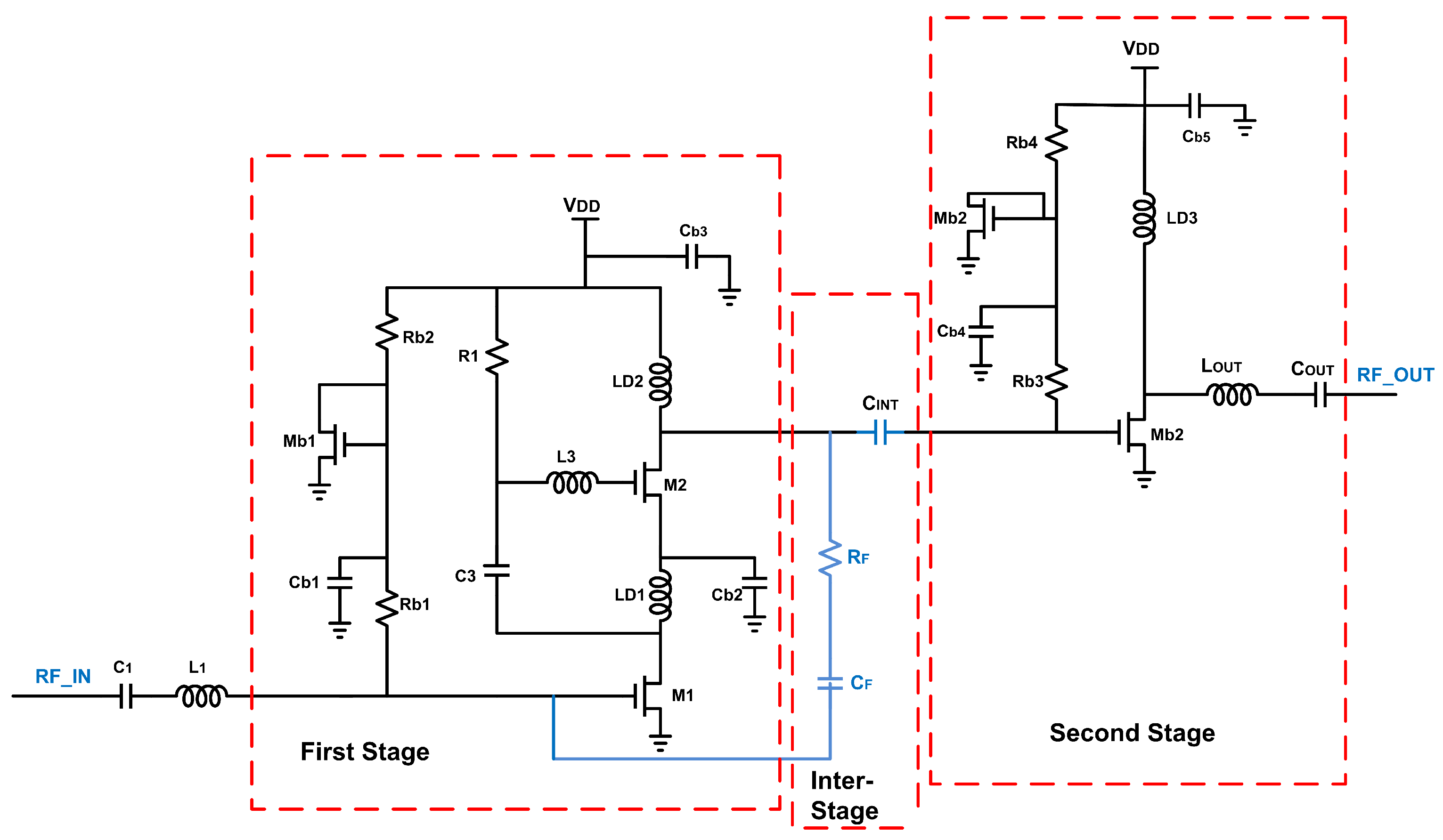
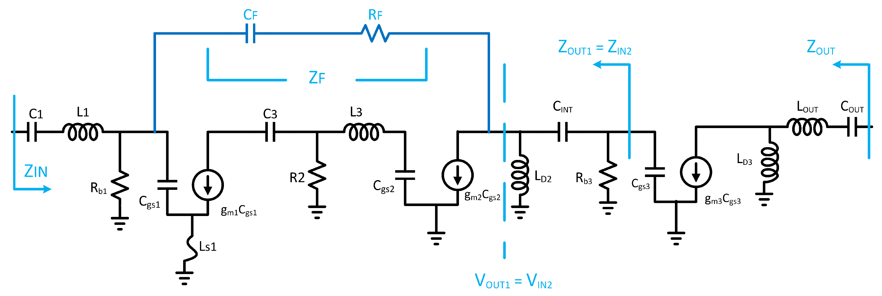
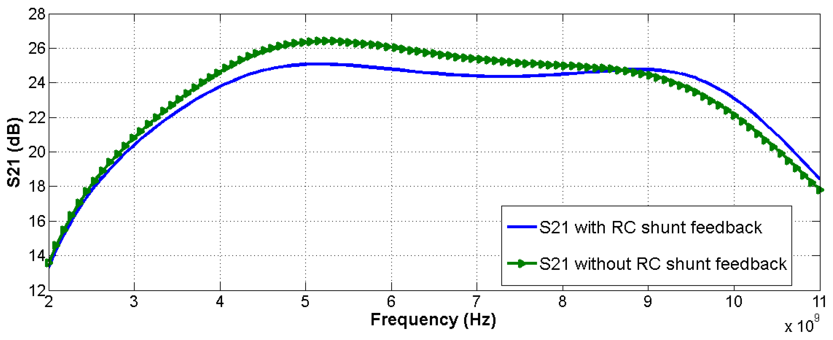
The proposed UWB-PA design and its small signal-equivalent circuit are shown in Figure 2 and Figure 3, respectively. The design adopts two-stage cascaded configuration of an amplifier with a proposed RC interstage for acquiring a sufficient power gain and wide bandwidth. The first stage involves the current-reuse cascade common source technique, and the second stage adopts the shunt peaking topology. The current-reuse structure has a power saving advantage compared to that of a cascade amplifier because the current of the transistor is reused by the transistor , so the gain is boosted without any additional power consumption. Based on the current reuse structure, the amplified signal at the drain of is passed to the gate of through the low impedance path formed by the series resonance of ( and ), in addition to the parasitic capacitance of the gate of . A large impedance of and a bypass capacitor block any RF signal from passing to the source of over the working frequency band. The current reuse structure suffers from the increment of parasitic capacitance, which degrades the PA gain performance, and therefore the two stages of amplifier are employed to reach a sufficient power gain while maintaining a low power consumption. The gain flatness can be improved by connecting the proposed RC interstage with , and between the first stage and the second stage. The feedback, and , can be optimized so that a good input match, broadband flatten gain, and low noise figure (NF) can be achieved simultaneously. The choice of the feedback resistor determines the operating bandwidth. A small value of the feedback resistor increases the operating bandwidth but decreases the gain. The optimum value of the resistor should be carefully chosen to meet the gain and matching demands. The effect of on the amplifier gain flatness is indicated in Figure 4. The second stage is a shunt peaking CS amplifier to enhance the gain, maximize the PAE, and realize the small group delay variation. The transistor size should be large for enhancing the output power. has peaking characteristics, which can widen the bandwidth and reduce the return loss of the output. networks of ( and ) and ( and ) are employed to improve the broadband input and output matching, respectively, over the entire bandwidth. Bypass capacitors to approximate a short circuit at high frequency and reject the effect of noise from the power supply. The resistor is used to supply a bias voltage for the transistor . The biasing circuit formed by , ,and to bias transistor and also , , and to bias transistor. Table 1 presents the size of the PA design parameters.
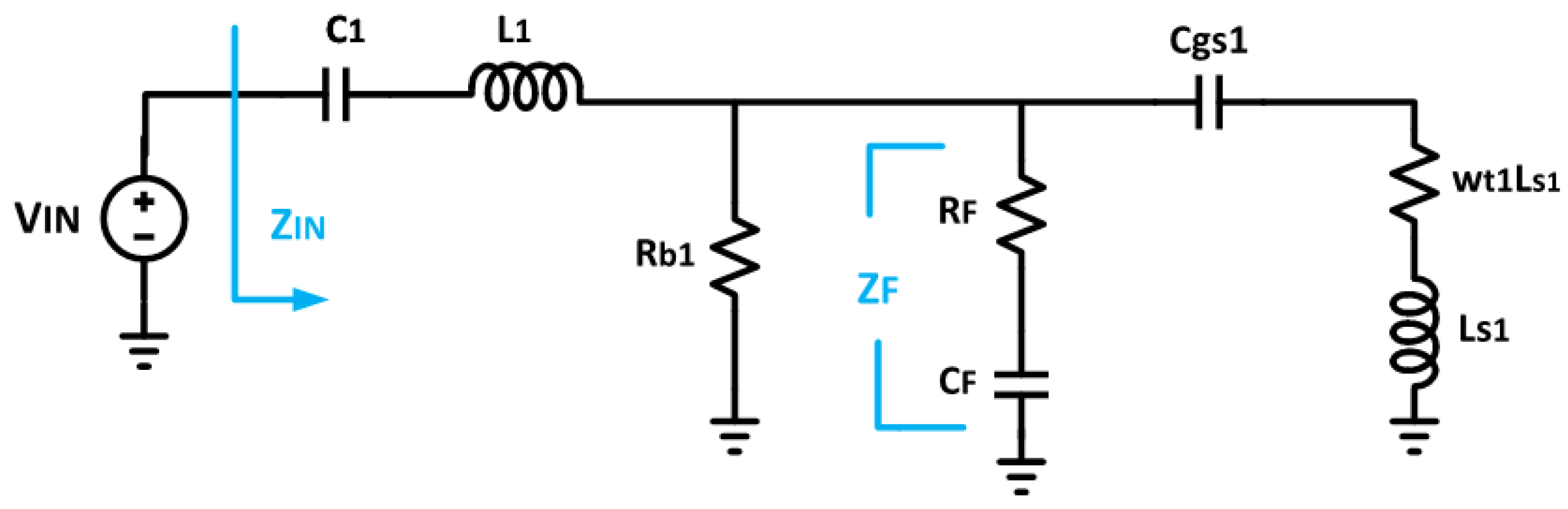
2.1. Input Matching
Wideband-input impedance matching is required to enhance the accessible power from the source to the PA to boost the UWB-PA PAE. The DC-blocking capacitor is a part of the input matching circuit with the inductor . The resistor and the capacitor helps in attaining wideband input matching. The small-signal equivalent circuit for the input impedance is shown in Figure 5. For simplicity, by neglecting the miller effect of the gate to drain capacitance , the input impedance is deduced as follows:
is the current gain cutoff frequency, is M1 transistor transconductance, and is the M1 transistor’s gate to source capacitance.
where;
is the voltage gain of the first stage. From Equation (3), the biasing resistor , network ( and ), and the feedback impedance were more carefully chosen, as smaller provides better matching but degrades the amplifier gain.
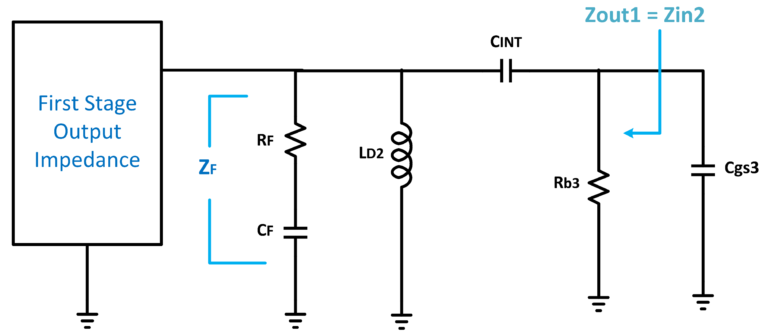
2.2. Interstage Impedance Matching
As presented in Figure 1, The RC circuit interstage matching is recommended in this work instead of the conventional LC matching circuit. The circuit , , and are optimized for maximizing the PAE that ensures the optimal power transfer through the amplifier stages. Figure 6 presents the small-signal equivalent circuit for the interstage impedance transformer. As outlined from Equation (6), , , , and are carefully optimized and chosen for a good impedance matching and high PAE, taking into account the gain flatness and group delay variation.
where;
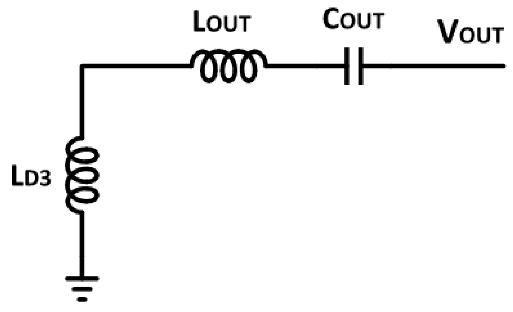
2.3. Output Matching
Figure 7 presents the small-signal equivalent circuit for the output impedance. The capacitor along with the inductor , and are optimized for enhancing the PAE and achieving a small-group delay variation. The equivalent output impedance is outlined by:
3. Simulation Results and Discussions
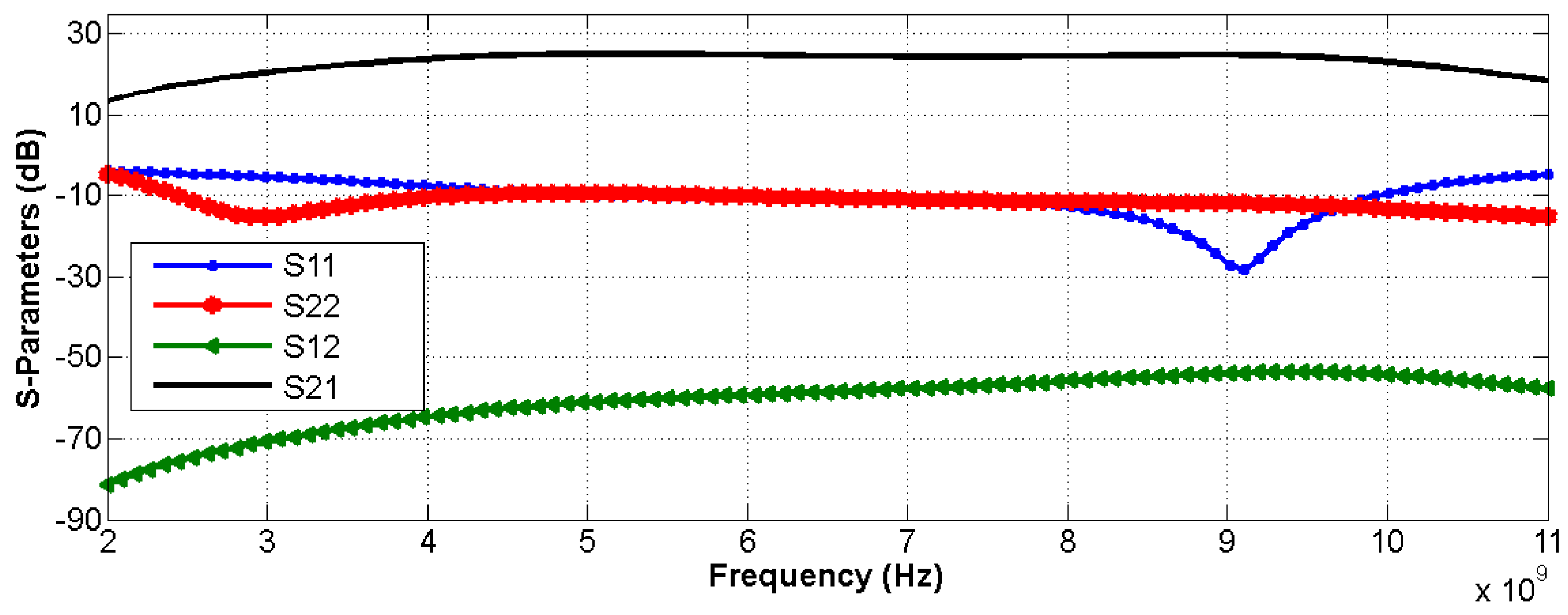
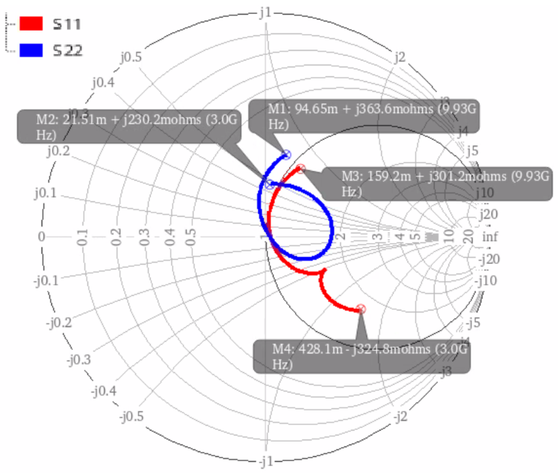
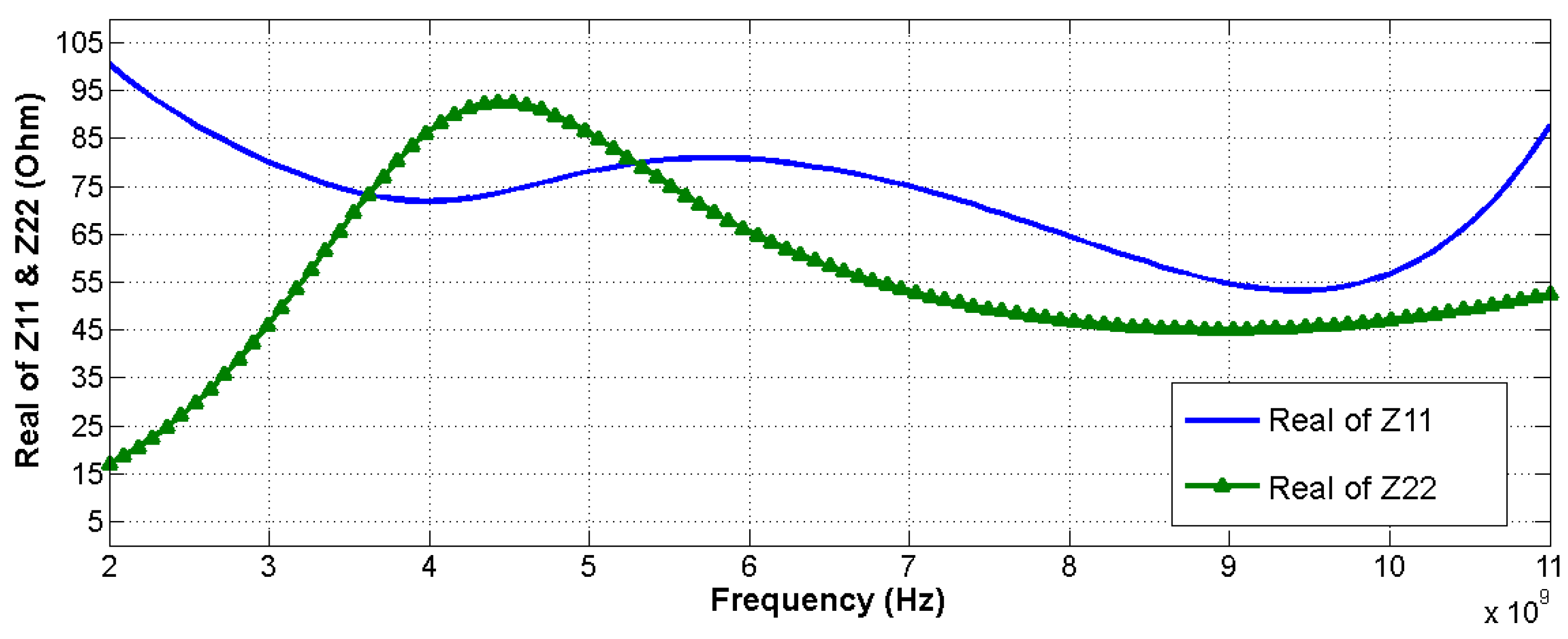
The proposed UWB-PA is simulated with cadence simulator in TSMC 65 nm CMOS process with 1.2 V supply voltage, consuming only the 15.5 mW DC power. Figure 8 shows the S-parameters postlayout simulation, where the input () and the output () return loss of below −7 dB and −10 dB, respectively, are achieved, and an average high flat power gain () of 22.8 ± 1.2 dB is realized over the full frequency band of 3.1 to 10.6 GHz. Figure 9 shows the frequency behavior of the normalized input and output matching ( and ) on Smith chart, while Figure 10 shows the impedance curves of both input and output matching networks. The optimal input and output impedance are around the 50 Ohms through the entire bandwidth.
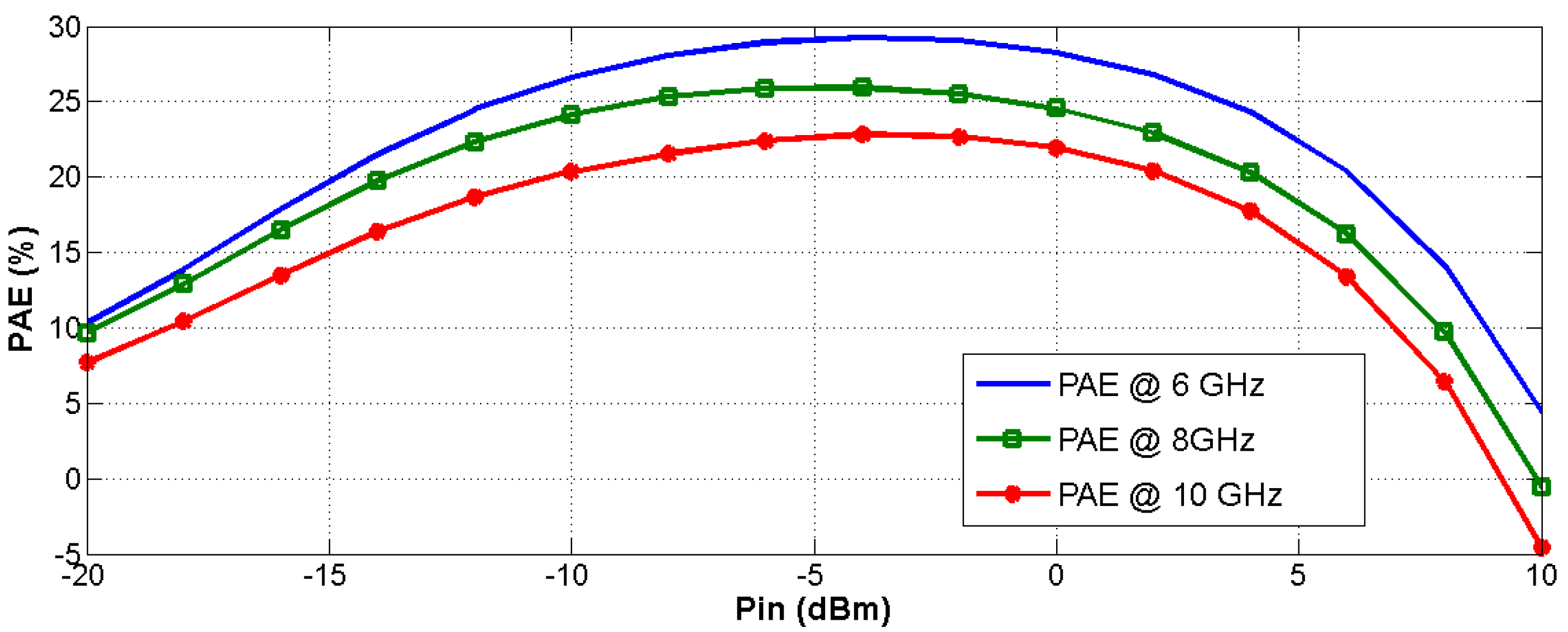
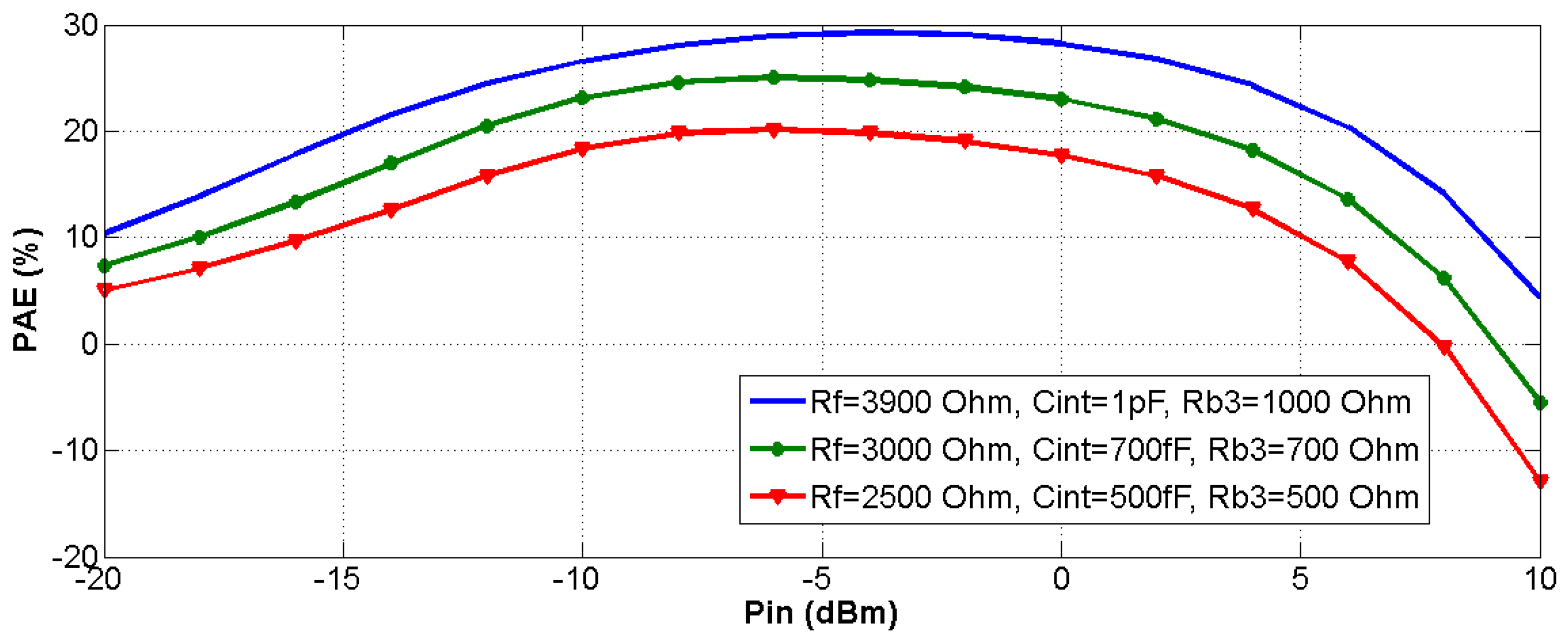
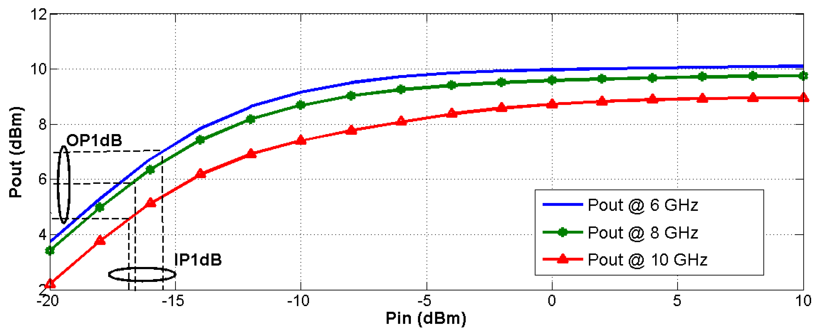
The PAE is a key parameter to measure the PA performance and is enhanced by improving the input, output, and interstage matching. Figure 11 demonstrates that the proposed UWB-PA attains the maximum PAE of 29.5% at 6 GHz, 26% at 8 GHz, and 22.6% at 10 GHz. By using Figure 12, to achieve a higher PAE, the values of , , and are reiterated several times and finally are selected to be 3.9 K, 1 pF, and 1 K, respectively. The proposed attains the saturated output power of about 10 dB at 6 GHz, 9.7 dBm at 8 GHz, and 8.9 dBm at 10 GHz. It also achieves 1-dB output compression point () of 6.8 dBm at 6 GHz, 5.7 dBm at 8 GHz, and 4.6 dBm at 10 GHz, respectively as displayed in Figure 13.
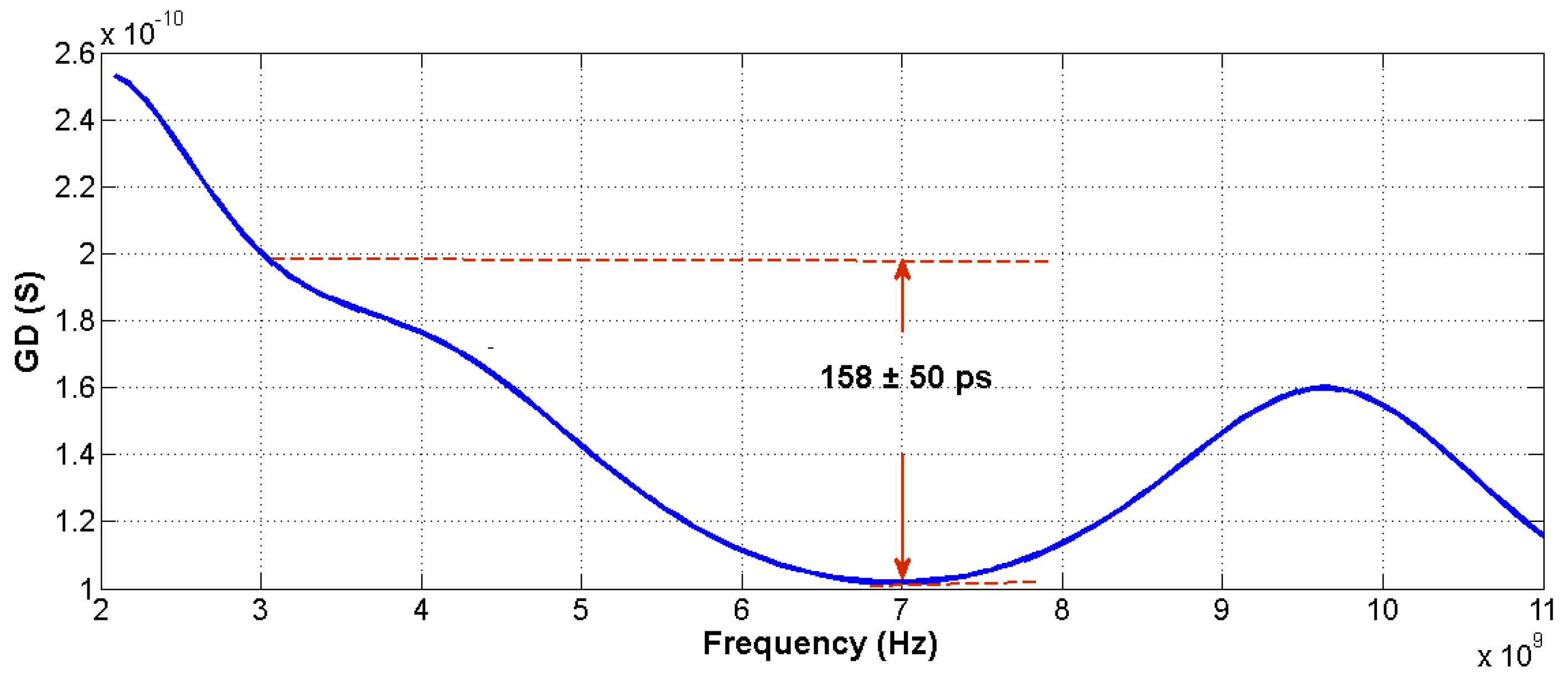
One of the major criteria used to measure the amplifier phase nonlinearity is the group delay (GD). In wideband communication, the GD variations should be kept low for better phase linearity. Minimizing the variations in the frequency domain saves the time domain amplified signal from distortion; besides, large variations GD implicate more phase distortion and the output does not retain its original input. Small variations of ±50 ps are achieved over the full desired band being indicated from the postlayout simulation, as shown in Figure 14, which indicates that all the frequencies will be delayed by an equal amount.
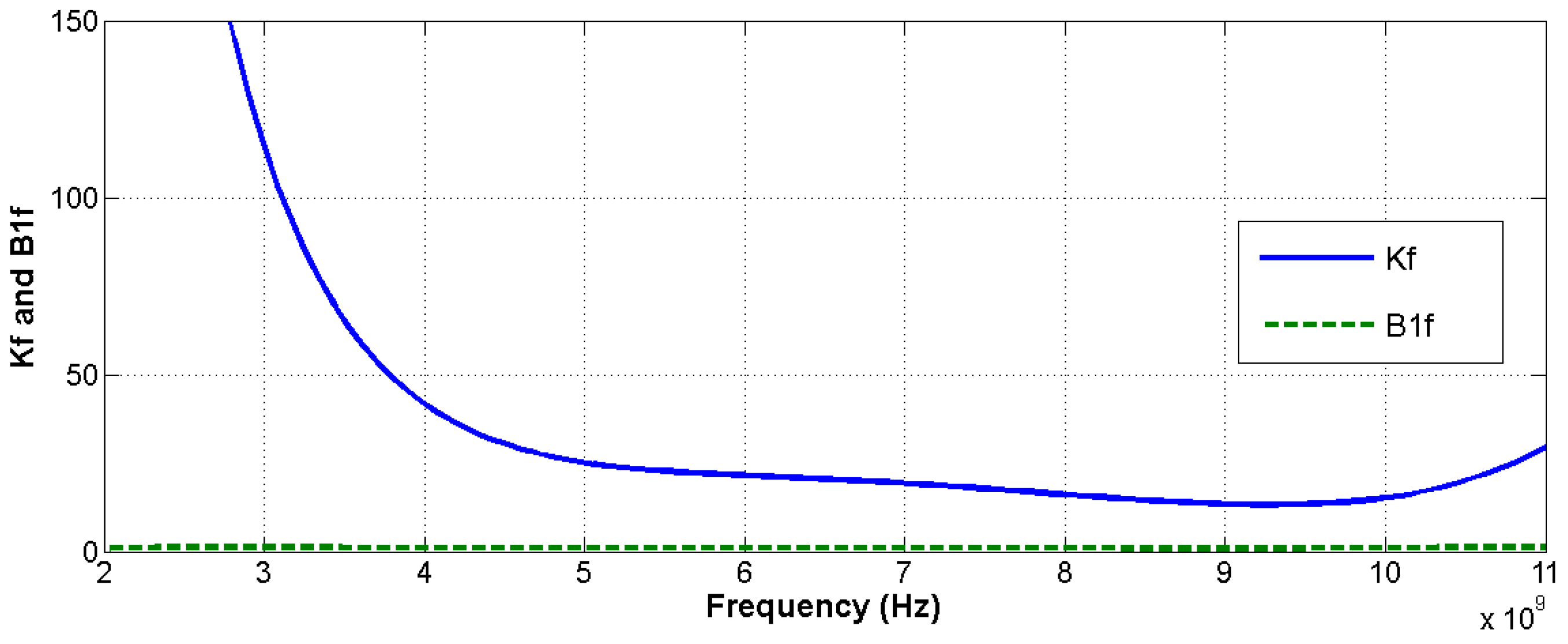
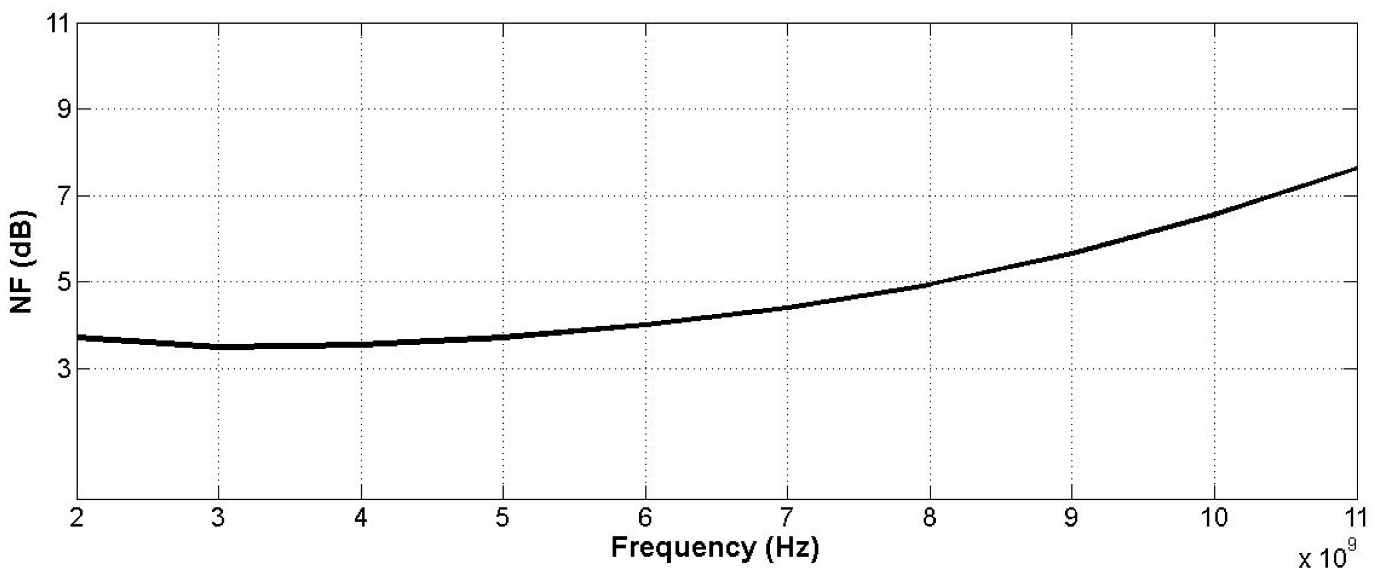
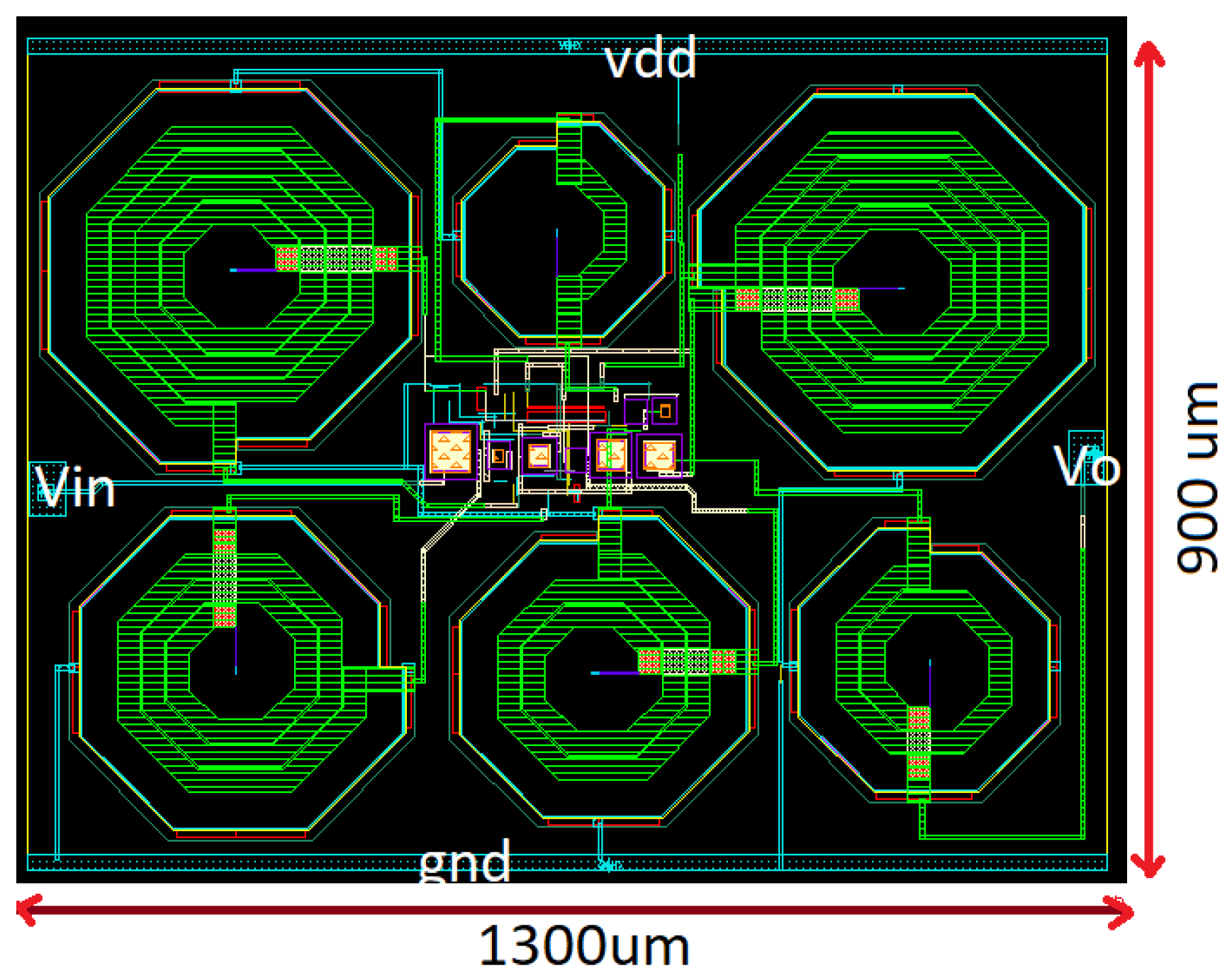
The Rollet’s condition, also known as the test, is used to determine the stability of the proposed power amplifier. A circuit will be unconditionally stable if > 1 and less than 1 are satisfied by the simulation test [15]. and of the PA are represented in Figure 15, and more than one and less than 1 are attained for the complete range, thereby ensuring that the PA is unconditionally stable. Figure 16 indicates the NF of less than 7 dB along with the full band. Noise figure reduction is a very good achievement, as it implies the good performance of the UWB-PA. Figure 17 presents the layout of the proposed PA, which occupies a chip area of 1300 um × 900 um. Table 2 shows the post-layout simulation results of the proposed UWB-PA and compares its performance with that of recently published UWB-PAs research. The proposed PA consumes the lowest power and has a small GD variation under the full band while attaining good gain flattens, high PAE, and good matching behavior.
4. Conclusions
In this work, A 3.1 to 10.6 GHz UWB 65 nm CMOS PA with the RC interstage is proposed to enhance the gain flatness and wideband matching. The proposed amplifier adopts the current reuse topology at the first stage for low power consumption and the shunt peaking topology at the second stage for gain and PAE enhancement. The postlayout simulation results show that the proposed PA consumes the low power of 15.5 mW at 1.2 V supply voltage. In addition, it achieves a small group delay variation of ±50 ps with a good flatten power gain of 22.8 ± 1.2 dB across the whole frequency band. Moreover, maximum PAE of 29.5% is attained.
Author Contributions
Conceptualization, M.A. and G.A.F.; Formal analysis, M.A., H.F.A.H. and G.A.F.; Writing—original draft, M.A. and G.A.F.; Writing—review and editing, H.F.A.H. and G.A.F. All authors have read and agreed to the published version of the manuscript.
Funding
This research received no external funding.
Conflicts of Interest
The authors declare no conflict of interest.
References
- Yuce, M.R.; Keong, H.C.; Chae, M.S. Wideband Communication for Implantable and Wearable Systems. IEEE Trans. Microw. Theory Tech. 2009, 57, 2597–2604. [Google Scholar] [CrossRef] [Green Version]
- Grewing, C.; Winterberg, K.; van Waasen, S.; Friedrich, M.; Puma, G.L.; Wiesbauer, A.; Sandner, C. Fully integrated distributed power amplifier in CMOS technology, optimized for UWB transmitters. In Proceedings of the 2004 IEE Radio Frequency Integrated Circuits (RFIC) Systems. Digest of Papers, Forth Worth, TX, USA, 6–8 June 2004. [Google Scholar]
- Harifi-Mood, M.; Avval, S.A.; Bijari, A.; Kandalaft, N. A Low-Power Tapered Matrix Distributed Amplifier for Ultra-Wide-Band Applications. In Proceedings of the 2020 11th IEEE Annual Information Technology, Electronics and Mobile Communication Conference (IEMCON), Vancouver, BC, Canada, 4–7 November 2020. [Google Scholar]
- Sapawi, R.; Sahari, S.K.; Kipli, K. A low power 3.1–10.6 GHz ultra-wideband CMOS power amplifier with resistive shunt feedback technique. In Proceedings of the 2013 International Conference on Advanced Computer Science Applications and Technologies, Kuching, Malaysia, 23–24 December 2013. [Google Scholar]
- Liu, J.; Cao, C.; Li, Y.; Tan, T.; Chen, D.; Huang, Z.; Li, X. A Broadband CMOS High Efficiency Power Amplifier with Large Signal Linearization. In Proceedings of the 2019 IEEE Asia-Pacific Microwave Conference (APMC), Singapore, 10–13 December 2019. [Google Scholar]
- Hsu, H.C.; Wang, Z.W.; Ma, G.K. A low power CMOS full-band UWB power amplifier using wideband RLC matching method. In Proceedings of the 2005 IEEE Conference on Electron Devices and Solid-State Circuits (EDSSC), Hong Kong, China, 19–21 December 2005. [Google Scholar]
- Sapawi, R.; Pokharel, R.K.; Mat, D.A.A.; Kanaya, H.; Yoshida, K. A 3.1–6.0 GHz CMOS UWB power amplifier with good linearity and group delay variation. In Proceedings of the Asia-Pacific Microwave Conference 2011, Melbourne, VIC, Australia, 5–8 December 2011. [Google Scholar]
- Wong, S.-K.; Maisurah, S.; Osman, M.N.; Kung, F.; See, J.-H. High efficiency CMOS Power Amplifier for 3 to 5 GHz Ultra-Wideband (UWB) Application. IEEE Trans. Consum. Electron. 2009, 55, 1546–1550. [Google Scholar] [CrossRef]
- Bhale, V.P.; Shah, A.D.; Dalal, U.D. 3–5 GHz CMOS Power Amplifier Design for Ultra-Wide-Band Application. In Proceedings of the International Conference on Electronics and Communication Systems, Coimbatore, India, 13–14 February 2014; pp. 1–4. [Google Scholar]
- Wang, L.Y.; Li, B.; Wu, Z.H. A low power CMOS power amplifier for implanted biomedical ultra wideband (UWB) applications. In Proceedings of the IEEE 11th International Conference on Solid-State and Integrated Circuit Technology (ICSICT), Xi’an, China, 29 October–1 November 2012. [Google Scholar]
- Chung, H.-W.; Hsu, C.-Y.; Yang, C.-Y.; Wei, K.-F.; Chuang, H.-R. A 6–10-GHz CMOS power amplifier with an interstage wideband impedance transformer for UWB transmitters. In Proceedings of the 2008 38th European Microwave Conference (EuMC), Amsterdam, The Netherlands, 27–31 October 2008. [Google Scholar]
- Sapawi, R.; Pokharel, R.K.; Murad, S.A.Z.; Anand, A.; Koirala, N.; Kanaya, H.; Yoshida, K. Low group delay 3.1–10.6 GHz CMOS power amplifier for UWB applications. IEEE Microw. Wirel. Compon. Lett. 2012, 22, 41–43. [Google Scholar] [CrossRef]
- Mosalam, H.; Allam, A.; Jia, H.; Abdelrahman, A.; Kaho, T.; Pokharee, R.K. 5.0 to 10.6 GHz 0.18 μm CMOS Power Amplifier with Excellent Group Delay for UWB Applications. In Proceedings of the 2015 IEEE MTT-S International Microwave Symposium, Phoenix, AZ, USA, 17–22 May 2015. [Google Scholar]
- Murad, S.A.Z.; Shahimim, M.M.; Pokharel, R.K.; Kanaya, H.; Yoshida, K. A 6–10.6 GHz CMOS PA with common-gate as an input stage for UWB transmitters. In Proceedings of the TENCON-IEEE Region 10 Annual International Conference, Bali, Indonesia, 21–24 November 2011. [Google Scholar]
- Roshani, S.; Roshani, S. Design of a high efficiency class-F power amplifier with large signal and small signal measurements. Measurement 2020, 149, 106991. [Google Scholar] [CrossRef]
- Mosalam, H.; Gadallah, A. High Efficiency, Good phase linearity 0.18 Ωm CMOS Power Amplifier for MBAN-UWB Applications. Int. J. Electr. Comput. Eng. Syst. 2021, 12, 131–138. [Google Scholar]
- Al-Kofahi, I.S.; Albataineh, Z.; Dagamseh, A. A two-stage power amplifier design for ultra-wideband applications. Int. J. Electr. Comput. Eng. (IJECE) 2021, 11, 772–779. [Google Scholar] [CrossRef]
- Sapawi, R.; Salleh, D.N.S.D.A.; Sahari, S.K.; Masra, S.M.W.; Mat, D.A.A.; Kipli, K.; Murad, S.A.Z. High Gain of 3.1–5.1 GHz CMOS Power Amplifier for Direct Sequence Ultra Wideband Application. J. Telecommun. Electron. Comput. Eng. 2016, 8, 99–103. [Google Scholar]
- Polge, D.; Ghiotton, A.; Kerherve, E.; Fabre, P. Low group delay variation 3–10 GHz 65 nm CMOS stacked power amplifier with 18.1 dBm peak 1 dB compression output power. Microw. Opt. Technol. Lett. 2017, 60, 400–405. [Google Scholar] [CrossRef]
Figure 1.
Block diagram of suggested ultra-wideband (UWB) power amplifier.

Figure 2.
Schematic of proposed UWB power amplifier.

Figure 3.
Small signal-equivalent circuit model.

Figure 4.
Simulated S21 with and without feedback resistor.

Figure 5.
Input impedance equivalent circuit.

Figure 6.
Interstage impedance matching network transform equivalent circuit.

Figure 7.
Output impedance equivalent circuit.

Figure 8.
Postlayout simulation of s-parameters (), (), (), and ().

Figure 9.
Frequency behavior of () and () on Smith chart.

Figure 10.
Impedance curves of input and output matching network ( and ).

Figure 11.
Simulated PAE versus at different frequencies within mentioned band.

Figure 12.
Effect of resistors and and capacitor on PAE.

Figure 13.
versus at different frequencies within desired band.

Figure 14.
Postlayout simulation of group delay.

Figure 15.
and simulation results.

Figure 16.
Noise floor (NF) simulation result.

Figure 17.
Layout of proposed PA.


Table 1.
Design parameter values of proposed UWB-PA.
| Design Parameter | Values | Design Parameter | Values |
|---|---|---|---|
| L = 0.06 µm, W = 100 µm | 1.2 nH | ||
| L = 0.06 µm, W = 100 µm | 3.7 nH | ||
| L = 0.06 µm, W = 100 µm | 3.7 nH | ||
| 2 pF | 610 pH | ||
| 50 fF | 200 | ||
| 1 pF | 400 | ||
| 500 fF | 1 K | ||
| 1 pF | 400 | ||
| 1.8 nH | 3.9 K | ||
| / | L = 0.06 µm, W = 60 µm | 186 pH |
Table 2.
Postlayout simulation results of proposed UWB-PA in comparison with that of other published CMOS UWB-PAs.
Table 2.
Postlayout simulation results of proposed UWB-PA in comparison with that of other published CMOS UWB-PAs.
| Ref. | [4] * | [16] * | [17] * | [18] * | [19] ** | This Work * |
|---|---|---|---|---|---|---|
| CMOS Technology (nm) | 180 | 180 | 180 | 130 | 65 | 65 |
| frequency (GHz) | 3.1–10.6 | 3.1–10.6 | 3–5 | 3.1–5.1 | 3–10 | 3.1–10.6 |
| Gain (dB) | 12.4 ± 1.1 | 12.5 ± 1 | 16.2 | 20.3 ± 0.8 | 12.65 ± 1.25 | 22.8 ± 1.2 |
| S11 (dB) | <−8.6 | <−4.5 | <−6 | <−1.5 | <−10 | <−7 |
| S22 (dB) | <−8.6 | <−8.5 | <−0.5 | <−6 | <−10 | <−10 |
| Dissipated Power (mW) | 19 | 36 | 25 | 27.3 | N/A | 15.5 |
| GD (ps) | ±18.3 | ±50 | ±75 | ±121.3 | ±21.5 | ±50 |
| PAE (%) | N/A | 32.5 | 47 | N/A | 20.15 ± 7.55 | 29.5@6 GHz |
| OP1dB (dBm) | N/A | 11 | 10.1 | N/A | 16 ± 2.1 | 6.8 |
| Area (mm2) | 0.69 | 0.55 | N/A | N/A | 0.498 | 1.17 |
* Simulated. ** Measured
Publisher’s Note: MDPI stays neutral with regard to jurisdictional claims in published maps and institutional affiliations. |
© 2022 by the authors. Licensee MDPI, Basel, Switzerland. This article is an open access article distributed under the terms and conditions of the Creative Commons Attribution (CC BY) license (https://creativecommons.org/licenses/by/4.0/).
Share and Cite
MDPI and ACS Style
Ali, M.; Hamed, H.F.A.; Fahmy, G.A. Small Group Delay Variation and High Efficiency 3.1–10.6 GHz CMOS Power Amplifier for UWB Systems. Electronics 2022, 11, 328. https://0-doi-org.brum.beds.ac.uk/10.3390/electronics11030328
AMA Style
Ali M, Hamed HFA, Fahmy GA. Small Group Delay Variation and High Efficiency 3.1–10.6 GHz CMOS Power Amplifier for UWB Systems. Electronics. 2022; 11(3):328. https://0-doi-org.brum.beds.ac.uk/10.3390/electronics11030328
Chicago/Turabian StyleAli, Mayar, Hesham F. A. Hamed, and Ghazal A. Fahmy. 2022. "Small Group Delay Variation and High Efficiency 3.1–10.6 GHz CMOS Power Amplifier for UWB Systems" Electronics 11, no. 3: 328. https://0-doi-org.brum.beds.ac.uk/10.3390/electronics11030328
Note that from the first issue of 2016, this journal uses article numbers instead of page numbers. See further details here.