
Review on Physically Flexible Nonvolatile Memory for Internet of Everything Electronics

Abstract
:
1. Introduction

2. Approaches for Making Flexible Devices
2.1. The All-Organic Approach

2.2. The Hybrid Systems Approach


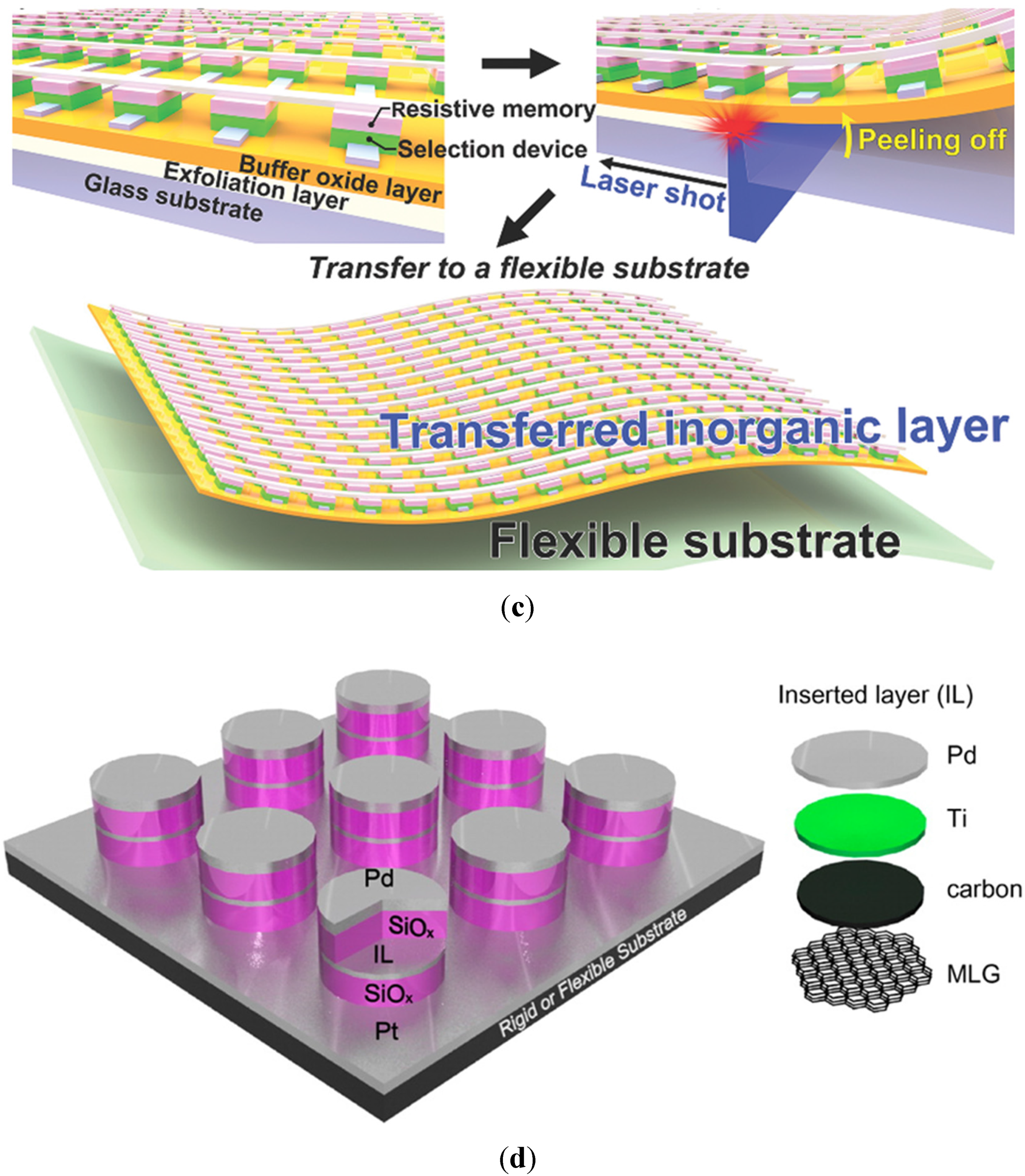
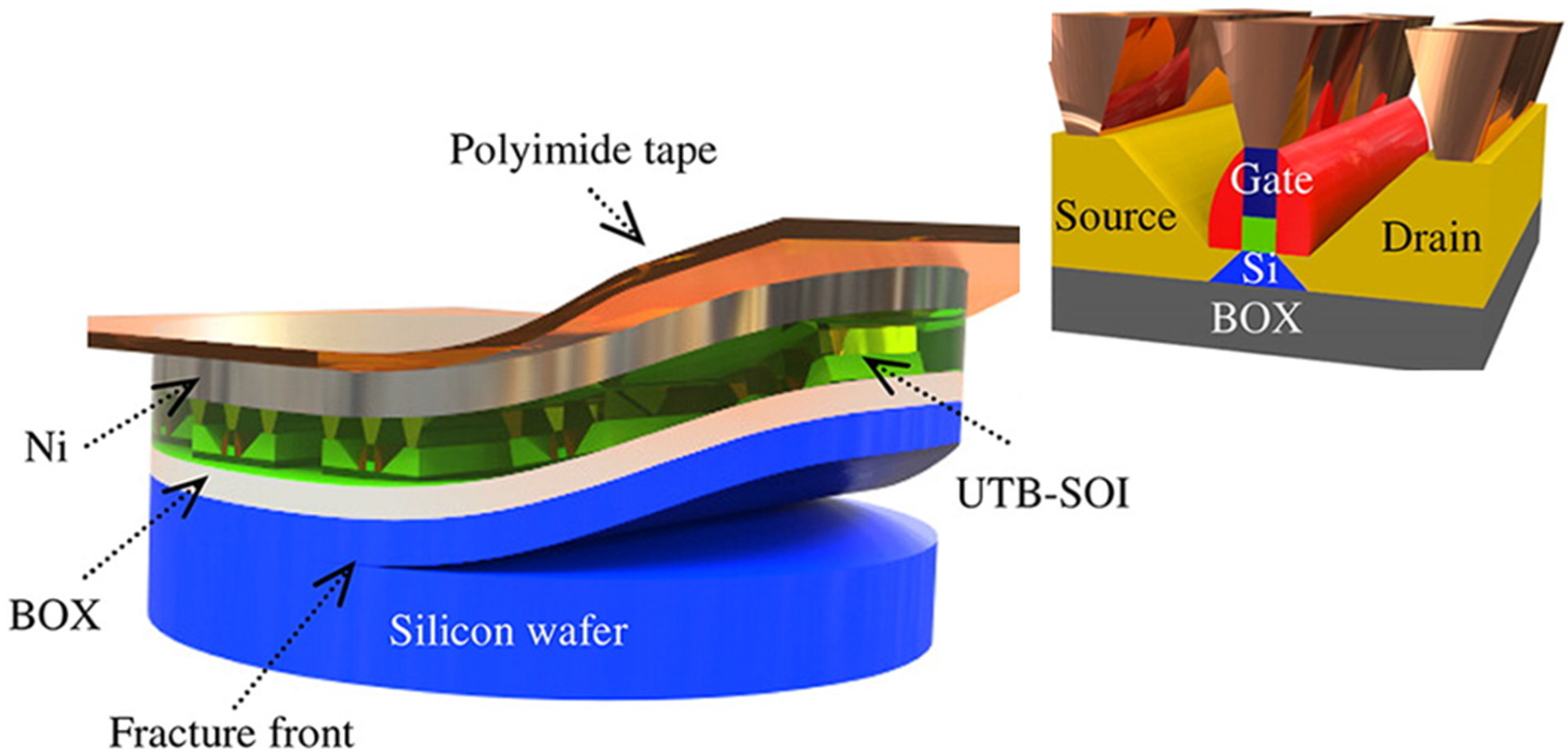
2.3. Spalling Technology

2.4. The Complementary Transfer-free Inorganic Approach


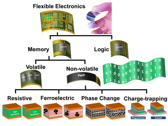
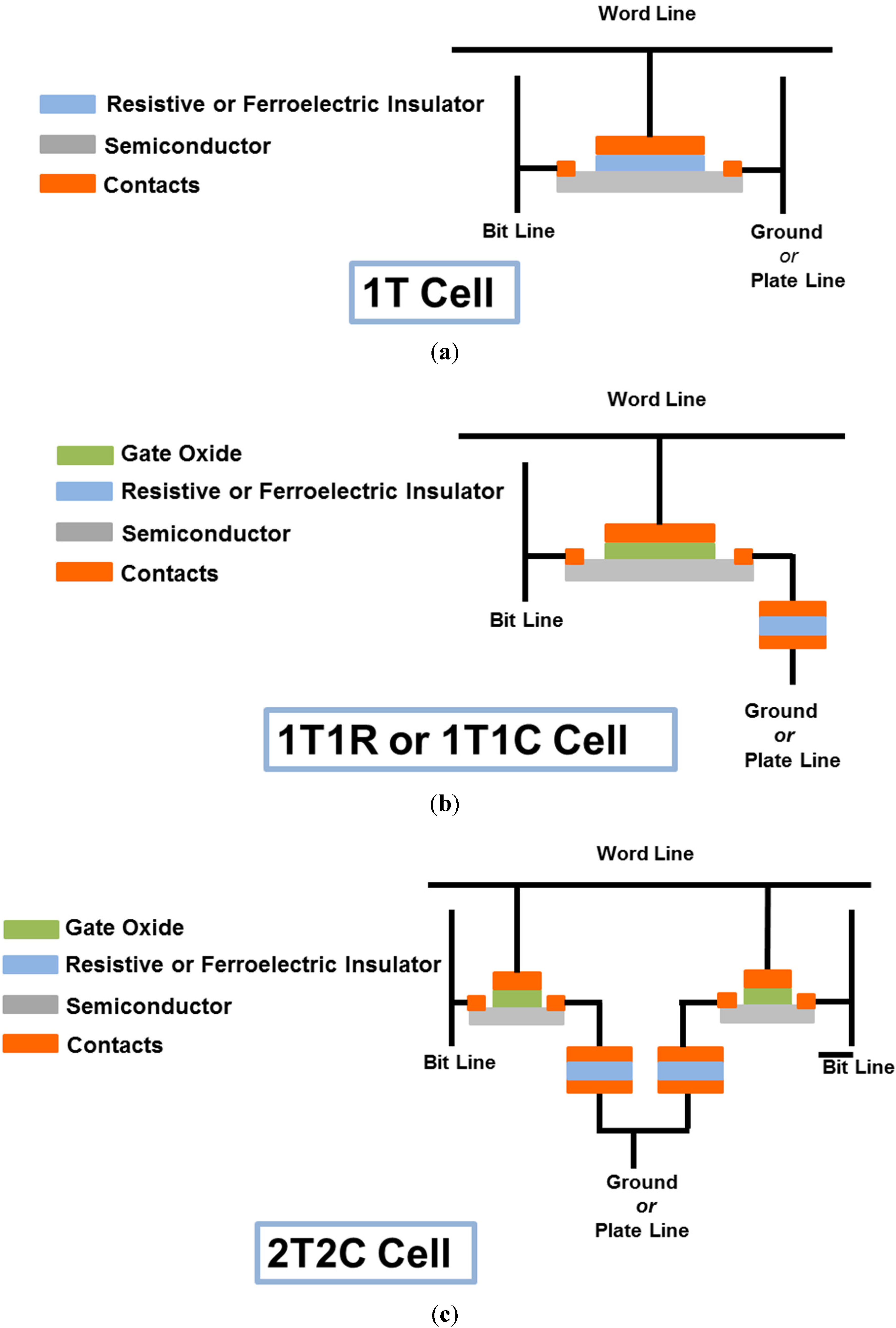
3. NVM Operational Principles and Architectures
3.1. NVM Operational Principles

| NVM Type | Operation Principle | Flexed | ||
|---|---|---|---|---|
| ReRAM (Memristor) | A resistive oxide is sandwiched between two metallic layers. The resistance of the oxide changes with applied “set” and “reset” voltage pulses. A high-resistance state corresponds to “0” and a low-resistance state corresponds to “1”. | Yes | ||
| FeRAM | A ferroelectric material has two possible polarization states inherent from its crystalline structure. Applying write/erase voltage pulse switches for positive to negative polarization states, corresponding to “0” or “1”. | Yes | ||
| MRAM | Spintronic devices such as magnetic tunneling junctions are composed of a fixed (“pinned”) magnetic moment layer, a tunneling barrier (oxide), and a free layer. Current flowing in nearby lines is expected to magnetize the free layer. If the free layer magnetic moment is parallel to that of the pinned layer, the device is “ON” and the resistance across the structure is low. If the free layer is magnetized such that its magnetic moment is anti-parallel to the pinned layer, the device is “OFF” and the structure will be in high-resistance state. | No | ||
| PCRAM | Current or laser pulses are applied to change the phase of a material from crystalline (low resistance) to amorphous (high resistance) and vice versa at a localized space, which changes the material’s electrical and optical properties. Short pulses above the melting temperature are needed to make the change from the crystalline to the amorphous phase, while longer pulses below the melting temperature are required to restore the crystalline order of the material. | Yes | ||
| Flash | FG | FG flash has the same structure as a field effect transistor (FET) except that its gate dielectric is split into three layers. The first is tunneling oxide, the second is an embedded conductor layer (i.e., doped polysilicon or embedded quantum dots (QDs) or metallic nanoparticles (NPs)) floating gate, and the third is a blocking oxide. When a programming voltage is applied, carriers tunnel from the channel to the floating gate. This results in a shift of the threshold voltage of the transistor corresponding to “1”. A reverse bias is applied during the erase operation to move the charges back into the channel. | Yes | |
| CT | The charge trap flash replaces the floating gate with a conductor layer that has an insulting layer (i.e., silicon nitride). The most common structures are the SONOS (Polysilicon-oxide-nitride-oxide-silicon) and the TANOS (titanium-alumina-nitride-oxide-silicon). | Yes | ||
| NEM-NVM | A nano-electromechanical switch is fabricated such that (i) upon applying a programming electrical signal, its pull-in voltage shifts when operated at a designed switching voltage or (ii) it has a free moving cantilever that has bistable physical states affecting its electrical properties. | No | ||
| Molecular Based NVM | A bistable molecule can be switched from a low-conductance state (“0”) to a high-conductance state “1” by applying brief bias voltage pulses to switch the state through oxidation and translation of the molecular structure between the two stable states. | No | ||


3.2. NVM Architectures


4. Flexible Field-Effect Transistors (FETs) for Logic and NVM Arrays
4.1. All-Organic Transistors
| Reference | [165] | [170] | [171] | [167] | [169] | [172] | [173] | [168] | [174] | [175] | [176] | [166] | [120] | [177] |
| Year | 2012 | 2012 | 2012 | 2010 | 2013 | 2013 | 2013 | 2014 | 2014 | 2015 | 2010 | 2014 | 2013 | 2015 |
| Structure | PEN/Ag gate BST dielectric/pentacene channel/Ag source and drain | PET/Al source and drain/C60 channel/Parylene-C dielectric/Al gate | Metal gate/Mylar/TIPS-pentacene/Metal source and drain | PI/Al gate/ hybrid (AlOx)-organic self-assembled monolayer (SAM) gate dielectric/Pentacene p-channel/Au source and drain | PET/ SWCNT/Ag source and drain/Barium titanate NP in PMMA ink dielectric/Ag gate | Au gate/Parylene dielectric/Au source and drain/TTC18-TTF channel | PI/gate electrode/Parylene dielectric/C8-BTBT channel/Au source and drain/Parylene/PI | PI/Al gate/c-PVP/c-PVP/Pentacene/ Au source and drain | PET/Ag source and drain/barium titanate -BTO-poly(methyl methacrylate) dielectric/Ag gate | PET/ITO gate/PVP dielectric/Pentacene channel/Au source and drain | PEN/Al gate/PI dielectric/QQT(CN)4/Cr-Au source and drain | PET/Ti-Au source and drain/Graphene/PMMA/Au gate | PAR/Au source and drain/P3HT:PEO-blend NW/ion-gel polyelectrolyte/Au gate | PEN/PVP/Ag gate/Parylene dielectric/Ag source and drain/DTBDT-C60 semiconductor |
| Approach | All organic | All organic | All organic | All organic | All organic (Ink-jet Printed) | All organic | All organic (Ink-jet Printing) | All Organic | All Organic (Screen Printing) | All Organic | All Organic | All Organic (Low Temperature Deposition + Graphene Transfer) | All organic | All organic |
| Dimensions (µm) | 100 × 2000 | 70 × 1800 | 50 × 500 | 85 × 1250 | 20 × 5000 | length is 20 | 150 × 1500 | 105 × 1000 | 100 × 500 | 45 × 4000 | 10 to 20 length | 0.34 × 0.31 | 90 × 1100 | |
| Mobility (cm2/VS) | 0.53–1.24 | 0.58 | 0.1 to 0.4 | 0.5 | 9 | 0.0043 | 0.15 | 0.56 | 7.67 | 0.45 | 0.1 to 0.006 | 340 | 9.7 | 1.9 |
| SS (mV/Dec) | 100–160 | 1250 | 5000 | 166 | ~3300 | 2300 | 1000 to 1500 | 250 | 170 | |||||
| Vth (V) | −1.11 to −1.18 | −0.1 | ~10 to 30 | ~−0.5 | 1.15 | 20 | ~10 | −0.82 | 0.5 | −0.16 | ||||
| Operation Voltage (V) | 3 | 10 to 40 | 3 | −10 to 10 | 10 to −50 | −4 to 4 | <10 | 10 to −30 | 100 to −100 | −60 to 40 | 2 | 20 | ||
| min bending radius (mm) | 3 | 5.1 | 0.26 unencapsulated and 0.11 encapsulated in Parylene | 0.1 | 1 | 2 | 1 | 0.75 | 3 | 2 | 5 | 10 | 6.25 | |
| ION/IOFF | 104 | 105 | 5 × 10³ | 1.5 × 10³ | 105 | 500 | 5 × 10⁴ | 105 | 104 to 105 | 105 | 108 | |||
| Yield | 66% | |||||||||||||
| Bending cycles | 104 |
| Reference | [178] | [179] | [180] | [181] | [182] | [183] | [184] | [28] | [185] | [186] | [187] | [188] | [189] | [190] | [191] | [192] | [193] |
| Year | 2013 | 2014 | 2013 | 2014 | 2014 | 2014 | 2014 | 2014 | 2011 | 2012 | 2013 | 2014 | 2014 | 2015 | 2015 | 2015 | 2013 |
| Structure | Parylene/Au gate/Parylene dielectric/pentacene channel/Au source and drain | Au source and drain/ (P(NDI2OD)T2 or N2200) n-type or (pBTTT) p-type/PMMA dielectric/Au gate | PVA/PMMA/Au source and drain/MoS2/Al2O3/Cu gate | PEN/Buffer/Al gate/Al2O3/a-IGZO/Mo-Al-Mo source and drain/PR protection | PI/Ni gate/PVP/Al2O3/a-IGZO/Ni source and drain | PDMS/CuPc NW/metal source and drain/Si3N4/Metal Gate | PI/Cu and MoTi Source and drain/organic semiconductor OSC active/organic gate insulator OGI/Cu gate | PI/ Inorganic Si FinFET | PI/IGZO TFT/PI | PI/SiO2-SiNx-SiO2-SiNx-SiO2/Mo gate/ Hybrid organic-inorganic S-ALO/Au Source and Drain/TIPS PEN:PS Channel | PI/IGZO TFT | Kapton Tape/IZO TFT/ | CPI/IGZO TFT | PI/ZnO TFT | PI/PVP/Al gate/PVP/ZrO2:B/In2O3/Al | PVP/AlOx /aZITO/AryLite | Kapton/PI/Ti/Pd/Al2O3 or HfO2/MOS2/Ti/Au |
| Approach | Hybrid (Transfer) | Hybrid (Transfer) | Hybrid (Transfer) | Hybrid (Deposition at Low Temperature) | Hybrid (Deposition at Low Temperature) | Hybrid (Transfer) | Hybrid (Transfer) | Hybrid (Transfer) | Hybrid (Transfer + encapsulation) | Hybrid (Detachment from Glass Substrate) | Hybrid (Deposition at Low Temperature) | Hybrid (Deposition at Low Temperature) | Hybrid (Deposition at Low Temperature) | Hybrid (Deposition at Low Temperature + Stripping off Si | Hybrid (Deposition at Low Temperature) | Hybrid (Deposition at Low Temperature) | Hybrid (Deposition at Low temperature) |
| Dimensions (µm) | 2 to 10 gate length | 20 × 1000 | 4.3 × 10 | 100 × 100 | 60 × 800 | 10 × 200 | 6 × (14–−160) | 0.25 × 3.6 | 115 × 280 | 4 × 20 to 6000 | 6 × 50 | 50 × 1000 | L 20 × W 10 | 20 × 200 | 50 × 1000 | 1 × 3 | |
| Mobility (cm2/VS) | 0.0013 to 0.00022 | 0.1 to 0.3 | 19 | 11.2 | 5.3 to 8.39 | 2 | 0.34 | 141.53 (N) to 13.22 (P) | 13.7 | 0.61 | 18 | 6 to 11.2 | 12.7 | 12 | 0.42 | 10.9 | 30 |
| SS (mV/Dec) | ~5000 | 250 | 270 | 520 to 960 | 80 (N) to 70 (P) | 200 | 2000 to 4600 | 160 | 82 | ||||||||
| Vth (V) | −4 to 9.5 | −2.12 | 0.5 | 7.03 to 9.8 | 0.345 (N) to 0.713 (P) | 0.154 | −0.27 | 0.9 | 18.8 to 31.3 | −1.7 | 8.07 | 0.7 | −2 | ||||
| Operation Voltage (V) | −32 | 20 to 50 | −5 to 2 | 10 to 10 | 20 to −10 | −10 | 30 to −30 | −1.5 to 1.5 | 5 | 0.5 to 2 | 5 | −20 to 20 | 8 | −40 to 40 | 3 | 3 | |
| Switching time (ms) | <0.8 × 10⁻³ | ||||||||||||||||
| min bending radius (mm) | 0.4 to 0.8 | 1 | 5 | 10 | 10 | 3 | 4 | 5 | 0.125 | 2 | 5 | 10 | 2 | 3.3 | 5 | 10 | 1 |
| ION/IOFF | 104 | 105 | 106 | 109 | 1.4 × 10⁵ to 3.5 × 10⁶ | 104 | 107 | 104.6 (N) to 104.78 (P) | 107 | 3.8 × 10⁴ to 1.5 × 10⁶ | 108 | 3.69 × 10⁵ | 105 | 107 | |||
| Yield | 90% | 60% | |||||||||||||||
| Bending cycles | 10 | 106 | 105 | 450 | 105 | 5000 | 1000 | 1000 | 5 × 10⁴ | 104 | 100 |
4.2. Hybrid Transistors
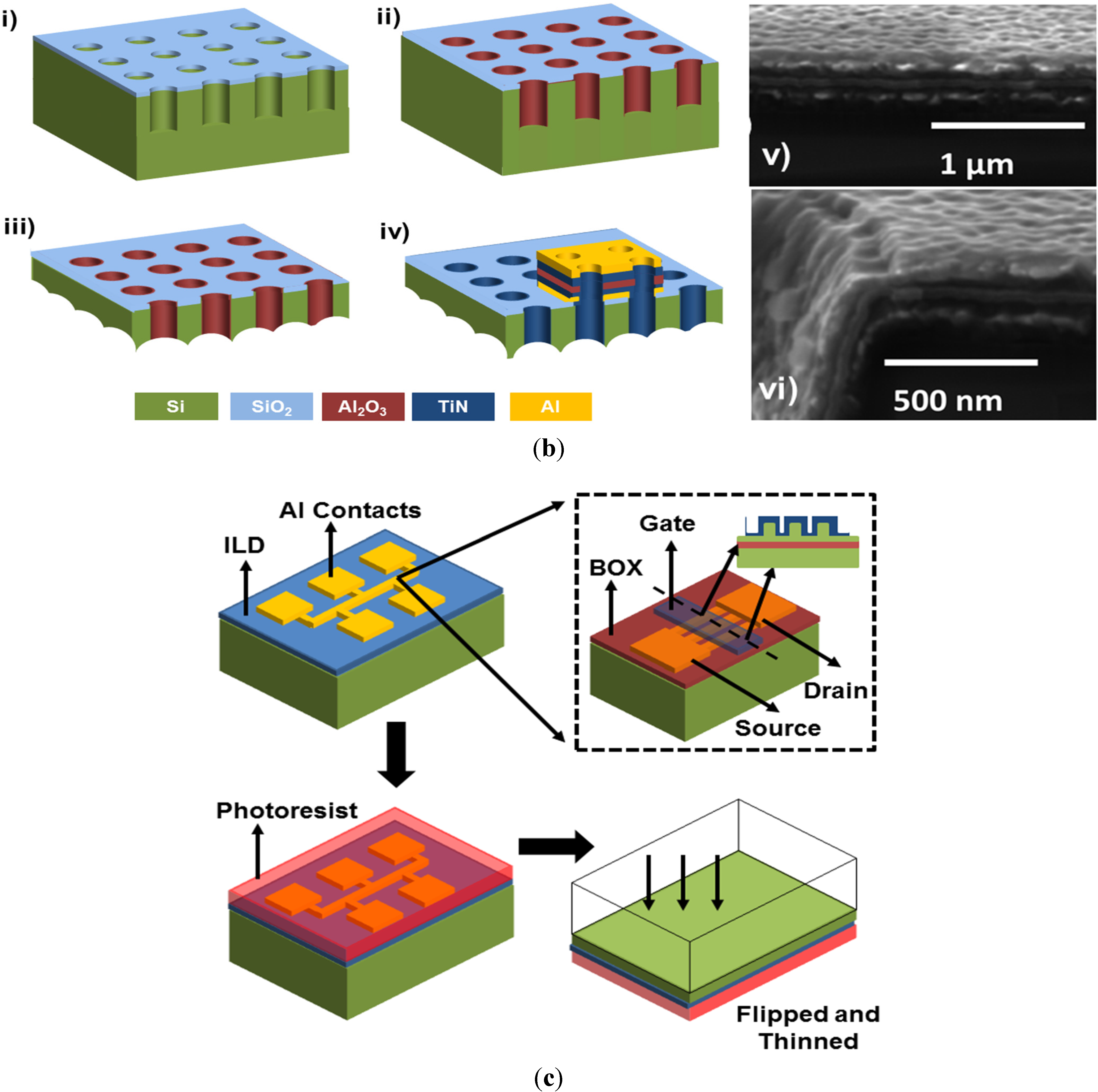
4.3. Inorganic Transistors on Flexible Silicon
| Reference | [194] | [45] | [125] | [195] |
| Year | 2013 | 2014 | 2012 | 2012 |
| Structure | Si/NiSi/Al source and drain/Al2O3 dielectric/TaN-Al gate | Inorganic FinFETs on Thinned Si | Inorganic Planar MOSFETs on Exfoliated Si | Inorganic Planar MOSFETs on Thinned Si |
| Approach | Inorganic (Etch-protect-Release) | Inorganic (Soft Back Etch) | Inorganic (Exfoliation) | Inorganic (Spalling) |
| Dimensions (μm) | 8 length × 5 width | 0.25 (P) to 1 (N) × 3.6 | 0.15 to 1 length | 0.03 length |
| Mobility (cm2/VS) | 43 | 102 (P) | 252 (N) to 51 (P) | |
| SS (mV/Dec) | 80 | 150 (N) to 63 (P) | 81 (P) to 72 (N) | |
| Vth (V) | −0.44 | 0.36 (N) to −0.556 (P) | 0.25 | |
| Operation Voltage (V) | 1 to −2 | −1.25 to 1.25 | −1 to 1 | 0.6 |
| Switching time (ms) | <16 × 109 | |||
| min bending radius (mm) | 0.5 | 6.3 | ||
| ION/IOFF | 104 | 105 | 106 (P) | 105 |
| Yield | 75% | |||
| Bending cycles | 5 | 200 |
5. Flexible NVM Technologies
- a)
- Form Factor (F2): Although form factor usually refers to the physical lateral (length and width) and vertical (height) dimensions for memory module millimeters, at the device level, the form factor is defined as the lateral area of a single memory cell (1 bit) divided by the square of the smallest feature (technology node) and has no units. For example, a memory cell that is 1 × 0.5 μm2 built at the 0.25-μm node would have a form factor of 8F2.
- b)
- Density: The number of memory bits that fit per unit area.
- c)
- Cost ($/bit): The total cost to make memory modules divided by the number of integrated memory bits.
- d)
- Endurance: The number of write/erase cycles a memory cell undergoes before its performance degrades significantly.
- e)
- Retention: The retaining ability of a memory cell to store uncompromised information over time.
- f)
- Operation voltage: The maximum voltage required for a write/erase operation of a memory bit.
- g)
- Speed: The amount of time the memory cell needs to switch between different memory states (‘0’ or ‘1’).
- h)
- Memory window: Measures the distinguishability of the different memory states. Voltage-sensitive memory is proportional to the voltage shift, while current sensitive memory is proportional to the current ratio for different states.
5.1. Flexible ReRAM
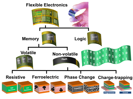
5.2. Flexible FeRAM
| Reference | [205] | [217] | [212] | [204] | [206] | [211] | [210] | [87] | [27] | [203] | [86] | [209] | [208] | [207] | [219] | [78] | [218] | [81] | [202] | [201] |
| Year | 2010 | 2012 | 2013 | 2012 | 2014 | 2015 | 2012 | 2010 | 2011 | 2010 | 2010 | 2012 | 2014 | 2012 | 2014 | 2015 | 2014 | 2012 | 2014 | 2015 |
| Memory Type | (1R) | (1R) | (1T) | (1R) | (1D1R) | (1R) | (1R) | (1R) | (1T1R) | (1R) | (1R) | (1R) | (1R) | (1R) | (1R) | (1R) | (1R) | (1D-1R) | (1R) | (1R) |
| Flexible Final Structure | PET/Ti/Au/Al/PI:PCBM/Al | PEN/Au/Ag2Se/Ag | PI/SiO2/Ti source and drain/a-IGZO/Ni gate | PEN/Al bottom/coPI layer/ Al top | PI/Si-p-n types diode/Cu/CuOx/Al | PET/ITO/WO3.H2O nanosheets/Cu | Glass/graphene/SiOx/Graphene | PES/Al/graphene-O/Al | Plastic/transferred Si channel material/Au source and drain-> on drainAl/TiO2/Al + Au for WL,BL, and SL | PET/ITO/PMMA/graphene/PMMA/Al | PET/ITO/graphene-O/Al | PES/Al/ZrO2/Al | Kapton/Cu/CuOx/Ag | PES/Cu/TiO2/Cu | Al foil/Ag-CNP(cellulose nanofiber paper)/Ag | PET/Au/Black Phosphorous Quant Dots (BPQD)-PVP/Ag | Si/SiO2/Al/TaN/Al2O3/TaN/Al | PI/Al/B-CNT and N-CNT in polystyrene/Al | PET/rGo/g-C3N4-NSs/rGo | Au/HKUST-1/Au/PET |
| Approach | All organic | Hybrid (low temperature deposition) | Hybrid (Deposition at Low Temperature) | All organic | Hybrid (Transfer + Low Temperature Deposition) | Hybrid (Low Temperature Deposition) | Hybrid (Low Temperature Deposition) | All organic | Hybrid (Transfer) | All organic | All organic | Hybrid (Low Temperature Deposition) | Hybrid (Low Temperature Deposition) | Hybrid (Deposition at Low Temperature) | Hybrid (Inorganic Flexible Substrate + Organic Device) | Hybrid (Deposition at Low Temperature) | Inorganic | All Organic | All Organic | All Organic |
| Operating Voltage (V) | 4.5 | −2 | −0.5 to +2 | −3 | +2 and +5 | −1.4 to +1 | 0 to +14 | −4 | −4 to +10 | −5 | −2 to +3 | −0.5 to 2.8 | −1 to +1 | 0 to 1.5 | −0.5 | −1.2 to +2.8 | −11 to +11 | 3 | 4.87 | 0.78 |
| Form Factor (F2) | -- | -- | 2 | -- | 11.1 | -- | -- | -- | 20 | -- | -- | -- | -- | -- | -- | -- | -- | -- | -- | -- |
| Memory Window (V) | -- | -- | 1 | -- | 1 | -- | -- | -- | 4 | -- | -- | -- | -- | -- | -- | -- | -- | -- | -- | -- |
| Speed (ns) | -- | 500 × 103 | 1000 | 5 × 10⁶ | -- | 50 | -- | -- | 106 | -- | -- | -- | -- | -- | -- | -- | -- | -- | -- | |
| Endurance (cycles) | 50 | 104 | 106 | 104 | 100 | 5000 | 400 | 100 | 100 | 1.5 × 10⁵ | 100 | 778 | 100 | -- | 100 | -- | -- | 100 | 50 | 106 |
| Retention (s) | 104 | 105 | 104 | 104 | 105 | 105 | 5 × 10⁴ | 105 | 104 | 105 | 5 × 10⁶ | 105 | 120 × 104 | -- | 105 | 1.1 × 10³ | -- | 105 | 5000 | 104 |
| Operating temperature (°C) | 25 | 200 | 85 | 25 | 25 | 25 | 25 | 25 | 25 | 25 | 25 | 25 | −18 to 82 | -- | 25 | 25 | 25 | 25 | 25 | −70 to +70 |
| Bending Radius (mm) | 9 | 16 | 10 | 5 | 10 | 8 | 6 | 7 | 5 | 10 | 4 | -- | 5 | 10 | 0.35 | -- | 1 | 10 | 8 | 3.2 |
| Bending Cycles | 140 | 100 | 1000 | 1000 | 1000 | 2000 | 300 | 1000 | 1000 | -- | 1000 | -- | 1000 | 100 | 1000 | -- | -- | 500 | 1000 | 160 |
| Yield | -- | -- | -- | 95%–99% | 85%–90% | -- | 70% | 80% | 60% | -- | -- | -- | -- | -- | -- | -- | -- | -- | -- | -- |
| Cell Dimensions (µm) | -- | -- | 10 × 20 channel | 200 × 200 | 150 × 300 channel | -- | 100 diameter | 50 × 50 | 10 × 200 | 17.74 to 26.71 diameter | -- | -- | 20 × 20 | -- | 50 × 50 | 500 × 500 | 100 × 100 | -- | 1000 × 3000 | 100 diameter |
| 600 × 600 | 500 cell | 500 × 500 | 250 × 250 |
| Reference | [84] | [231] | [235] | [232] | [233] | [236] | [229] | [237] | [238] | [239] | [240] | [230] | [241] | [242] | [243] |
| Year | 2013 | 2010 | 2012 | 2011 | 2011 | 2013 | 2015 | 2011 | 2011 | 2012 | 2012 | 2012 | 2015 | 2014 | 2013 |
| Memory Type | Ferroelectric (1T) | Ferroelectric (1C) | Ferroelectric (1C) | Ferroelectric (1T) | Ferroelectric (1T) | Ferroelectric (1C) | Ferroelectric (1C) | Ferroelectric (1C) | Ferroelectric (1C) | Ferroelectric (1T) | Ferroelectric (1C) | Ferroelectric (1C) | Ferroelectric (1R) | Ferroelectric (1T) | Ferroelectric (1T) |
| Flexible Final Structure | PI/Su-8/SiO2/Pt gate electrode/ PZT/graphene channel/ Cr-Au for source and drain electrodes | Plastic/Cr-Au/Ti-Pt/PZT/Pt/Cr/Au | Al foil/ PVD-TrFE/ Au | PEN/Ti-Au-Ti soucre and drain/Al2O3/ZnO channel/Al2O3 interface dielectric/PVDF-TrFE ferroelectric/Au | Au/poly(vinylidene fluoride-trifluoroethylene)/Al2O3/ZnO/Ti/Au/Ti/poly(ethylene naphthalate) | ULTEM 1000B/PEDOT:PSS/P(VDF-TrFE)/PEDOT:PSS | Si/SiO2/Ti-Pt/PZT/Pt | PEN/PEDOT:PSS/P(VDF-TrFE)/PEDOT:PSS | PEN/Au/P(VDF-TrFE)/Au | Bank Note/PDMS/PEDOT:PSS bottom electrode/ P(VDF-TrFE) ferroelectric/ Pentacene channel/ Au soucre and drain | Ag/BaTiO3/PVDF-TrFE nanocomposites/Ag | Pt/PZT(200 nm)/SRO(30 nm)/Pt(200 nm) foil | PET/Ag ink/PVDF-TrFE/Ag ink | PDMS/Au source and drain/F8T2 organic semiconductor/PVDF-TrFE ferroelectric/ Al gate | PI/PVP/Au source and Drain/Polymer blend channel/PVDF-TrFE ferroelectric/Al gate |
| Approach | Hybrid (Transfer) | Hybrid (Transfer) | Hybrid (Transfer) | Hybrid (Low Temperature Deposition) | Hybrid (Low Temperature Deposition) | All organic (ink-jet printing) | Inorganic | All organic | All organic | All organic | Hybrid (inorganic/organic composite substrate and device) | Inorganic | All Organic | All Organic | All Organic |
| Operating Voltage (V) | −11 | −3 | −12 | −14 to +12 | −10 to +8 | −30 | −15 | −10 | −30 to +30 | −15 to +15 | −3.3 | −4 | 23 | −20 to +20 | −80 to +80 |
| Form Factor (F2) | 8 | -- | -- | 2 | 2 | -- | -- | -- | -- | 16.67 | -- | -- | -- | 3 | 1 |
| Memory Window (V) | 6 | -- | -- | 7.8 | 3.4 | -- | -- | -- | -- | 8 | -- | -- | -- | 11 | 35 |
| Speed (ns) | -- | -- | -- | 1 × 10⁹ | 2 × 10⁹ | 50 × 106 | 500 | 106 | 10 × 103 | -- | -- | -- | 108 | 108 | -- |
| Endurance (cycles) | 1000 | -- | -- | -- | -- | 45% polarization after 105 | 109 | 106 has 80% Pr | -- | 105 | -- | 107 | -- | 6 × 10⁴ | 100 |
| Retention (s) | 200 | -- | -- | 1.5 × 10⁴ | <104 | -- | 105 | -- | -- | 104 | -- | -- | -- | 2000 | 104 |
| Operating temperature (°C) | 25 | 25 | 25 | 25 | 25 | 25 | 200 | 25 | 25 | 25 | 25 | 25 | 25 | 25 | 25 |
| Bending Radius (mm) | 9 | 8 | 6 | 9.7 | 9.7 | -- | 5 | -- | 6.5 | -- | -- | -- | -- | 6 | -- |
| Bending Cycles | 200 | -- | 500 | 2 × 10⁴ | 2 × 10⁴ | -- | 1000 | -- | -- | -- | -- | -- | -- | -- | -- |
| Yield | -- | -- | -- | -- | -- | -- | 95% | -- | -- | 90% | -- | -- | -- | -- | -- |
| Cell Dimensions (µm) | 10 × 80 channel | 100 × 400 | 180 diameter | 20 × 40 channel | 20 × 40 channel | 60 × 60 | 100 × 100 | -- | 25 × 25 | 60 × 1000 channel | -- | 100 diameter | 30 × 30 | 20 × 60 | 20 × 20 |
| 250 × 250 | 50 × 50 |
| Property | Best Reported Value for PZT-based FeRAM |
|---|---|
| Switching Speed | Pico seconds regime for material switching [225,226] and 70 ns for actual arrays due to bit/word line capacitances [244] |
| Ferroelectric Capacitor’s Lateral Dimensions | 0.1 µm2 [245] |
| Switching Energy | 400 fJ/bit [246] |
| Retention | >10 years @ 85 °C [247] , experimentally three days (2.5 × 10^5) was demonstrated for FeRAM (using SrBi2Ta2O9(SBT)) [248,249] |
| Technology Node (CMOS Logic) | 130 nm [247] |
| Operation Voltage | 1.5 Volts [246] |
| Read/Write Cycles | >1015 [250,251] |
5.3. Flexible PCRAM
| Reference | [252] | [253] | [254] | [255] |
| Year | 2010 | 2011 | 2012 | 2015 |
| Memory Type | PCRAM (1R) | PCRAM (1R) | PCRAM (1R) | PCRAM (1D-1R) |
| Flexible Final Structure | PI/TiN/GST/Pt probe tip | PET or PI or Stainless steel/ TiW bottom electrode/GST (Ge2Sb2Te5)/Cr top electrode | GFR Hybrimer Film/TiN/Pt/TiN/IST/Ps-b-PMMA/Cr | BCP/Transferred Si Diode/TiW bottom electrode/GST/SiOx cylinders/TiN/TiW top electrode |
| Approach | Hybrid (Low Temperature Deposition + Transfer by Hot Embossing and Nano Imprint Lithography -NIL) | Hybrid (Low Temperature Deposition + NIL) | Hybrid (Low Temperature Deposition) | Hybrid (transfer + low temperature deposition) |
| Operating Voltage (V) | 1.8 | 3 | 1.8 | 8.5 |
| Form Factor (F2) | -- | -- | -- | -- |
| Memory Window | -- | -- | -- | -- |
| Speed (ns) | 30 | 200 | 100 | 1000 |
| Endurance (cycles) | -- | -- | -- | 100 |
| Retention (s) | -- | -- | -- | 104 |
| Operating temperature (°C) | 25 | 25 | 25 | 25 |
| Bending Radius (mm) | -- | -- | 2.25 | 10 |
| Bending Cycles | -- | -- | -- | 1000 |
| Yield | -- | -- | -- | 66% |
| Cell Dimensions (μm) | 0.2 to 0.3 diameter | 0.25 diameter | 0.035 diameter | -- |
5.4. Flexible Flash
6. Conclusions and Future Prospects
| Reference | [260] | [82] | [80] | [76] | [77] | [262] | [74] | [85] | [73] | [261] |
| Year | 2012 | 2011 | 2012 | 2014 | 2011 | 2012 | 2010 | 2012 | 2013 | 2015 |
| Memory Type | Flash + Nano Particles (1T) | Flash (1T) | Flash (1T) | Flash (1T) | Flash (1T) | Flash (1T) | Flash (1T) | Flash (1T) | Flash (1T) | Flash (1T) |
| Flexible Final Structure | PET/Ag gate electrode/Al2O3/PMMA with Au NP composite/Pentacene/Au source and drain electrodes | PET/graphene gate electrode/Al2O3/CNT channel/graphene for source and drain electrodes | PES/Si NW/Al2O3/Pt-NP//Al2O3/Al source, drain, and gate | PET/ P(NDI2OD-T2) Channel/ Au source and drain/PVA tunneling dielectric/ Au-NP/ P(VDF−TrFE−CFE) blocking dielectric/ Al gate | PES/ITO gate/PVP blocking/APTES-Au-NP/PVP tunneling/MoO3 buffer/ Pentacene channel/ITO source and drain | PES/Al source and drain/ZnOPDA/AlOx-SAOLs/Zno:Cu/AlOx-SAOLs/Pentacene/ Al gate | PES/Ti-Au gate/ PVP blocking/ APTES-Au NP storage/PVP tunneling/ Pentacene channel/ Au source and drain | PEN/graphene channel/Al2O3/HfOx/Al2O3/ ITO | PET/ITO gate/Al2O3/Au NP charge trapping/Al2O3/PDPP-TBT/Au source and drain | PDMS/PI/Au/Al2O3-SiO2/SWCNT/Au |
| Approach | All organic | All organic | Hybrid (Transfer) | All organic | All organic | Hybrid (Low Temperature Deposition) | All organic | Hybrid (Deposition at Low Temperature) | All organic | Hybrid (Transfer) |
| Operating Voltage (V) | −5 to +5 | −10 to +10 | −10 to +10 | −6 to +6 | −90 to +90 | −15 to +15 | −90 to +90 | −21 to +23 | −40 to +40 | −25 to +25 |
| Form Factor (F2) | 10 | -- | -- | 20 | 10 | 2 | 10 | 6.67 | 20 | 11 |
| Memory Window | 2.1 | 10 | 1.85 | 2 | 15 | 14.1 | 9.7 | 8.6 | 7.5 | 13.2 |
| Speed (ns) | -- | 100 | 107 | 2 × 10⁹ | 1 × 10⁹ | 1 × 10⁸ | 1 × 10⁹ | hypothesized ~14 ns read time and 20 μs/20 ms write/erase time | 10 × 107 | 105 |
| Endurance (cycles) | 1000 | 500 | 104 | 105 | -- | -- | 700 | -- | 1000 | 104 |
| Retention (s) | 105 | 1000 | 104 | 105 | 105 | 1000 | 105 | 30% after 10 years | 106 | 104 |
| Operating temperature (°C) | 100 | 25 | 25 | 25 | 85 | 25 | 25 | degrades at 85 | 25 | 25 |
| Bending Radius (mm) | 10 | 8 | 16 | 9 | 20 | -- | 20 | 5 | 10 | 5 |
| Bending Cycles | 1000 | 1000 | 1000 | 100 | 2000 | -- | 1000 | 10 | 1000 | 1000 |
| Yield | -- | -- | -- | -- | -- | -- | -- | -- | -- | -- |
| Cell Dimensions (μm) | 50 × 500 channel | -- | 2 channel length | 100 × 2000 channel | 100 × 1000 channel | 50 × 100 channel | 100 × 1000 channel | 30 × 4.5 channel | 50 × 1000 channel | 18 × 200 |
Acknowledgments
Conflicts of Interest
References
- Zhou, H.; Seo, J.-H.; Paskiewicz, D.M.; Zhu, Y.; Celler, G.K.; Voyles, P.M.; Zhou, W.; Lagally, M.G.; Ma, Z. Fast flexible electronics with strained silicon nanomembranes. Sci. Rep. 2013, 3, 1291. [Google Scholar] [CrossRef] [PubMed]
- Des Etangs-Levallois, A.L.; Lesecq, M.; Danneville, F.; Tagro, Y.; Lepilliet, S.; Hoel, V.; Troadec, D.; Gloria, D.; Raynaud, C.; Dubois, E. Radio-frequency and low noise characteristics of SOI technology on plastic for flexible electronics. Solid-State Electron. 2013, 90, 73–78. [Google Scholar] [CrossRef]
- Nasr, B.; Wang, D.; Kruk, R.; Rösner, H.; Hahn, H.; Dasgupta, S. Flexible Electronics: High-Speed, Low-Voltage, and Environmentally Stable Operation of Electrochemically Gated Zinc Oxide Nanowire Field-Effect Transistors. Adv. Funct. Mater. 2013, 23, 1729–1729. [Google Scholar] [CrossRef]
- Han, S.T.; Zhou, Y.; Wang, C.; He, L.; Zhang, W.; Roy, V. Flexible Electronics: Layer-by-Layer-Assembled Reduced Graphene Oxide/Gold Nanoparticle Hybrid Double-Floating-Gate Structure for Low-Voltage Flexible Flash Memory. Adv. Mater. 2013, 25, 793–793. [Google Scholar] [CrossRef]
- Farsinezhad, S.; Mohammadpour, A.; Dalrymple, A.N.; Geisinger, J.; Kar, P.; Brett, M.J.; Shankar, K. Transparent anodic TiO2 nanotube arrays on plastic substrates for disposable biosensors and flexible electronics. J. Nanosci. Nanotechnol. 2013, 13, 2885–2891. [Google Scholar] [CrossRef] [PubMed]
- Majewski, L.; Grell, M.; Ogier, S.; Veres, J. A novel gate insulator for flexible electronics. Org. Electron. 2003, 4, 27–32. [Google Scholar] [CrossRef]
- McAlpine, M.C.; Friedman, R.S.; Lieber, C.M. High-performance nanowire electronics and photonics and nanoscale patterning on flexible plastic substrates. Proc. IEEE 2005, 93, 1357–1363. [Google Scholar] [CrossRef]
- Sun, Y.; Rogers, J.A. Inorganic semiconductors for flexible electronics. Adv. Mater. 2007, 19, 1897–1916. [Google Scholar] [CrossRef]
- Rogers, J.A.; Someya, T.; Huang, Y. Materials and Mechanics for Stretchable Electronics. Science 2010, 327, 1603–1607. [Google Scholar] [CrossRef] [PubMed]
- Sokolov, A.N.; Tee, B.C.K.; Bettinger, C.J.; Tok, J.B.H.; Bao, Z. Chemical and Engineering Approaches To Enable Organic Field-Effect Transistors for Electronic Skin Applications. Acc. Chem. Res. 2012, 45, 361–371. [Google Scholar] [CrossRef] [PubMed]
- Wang, C.; Hwang, D.; Yu, Z.; Takei, K.; Park, J.; Chen, T.; Ma, B.; Javey, A. User-interactive electronic skin for instantaneous pressure visualization. Nat. Mater. 2013, 12, 899–904. [Google Scholar] [CrossRef] [PubMed]
- Mei, Y.; Loth, M.A.; Payne, M.; Zhang, W.; Smith, J.; Day, C.S.; Parkin, S.R.; Heeney, M.; McCulloch, I.; Anthopoulos, T.D. High Mobility Field-Effect Transistors with Versatile Processing from a Small-Molecule Organic Semiconductor. Adv. Mater. 2013, 25, 4352–4357. [Google Scholar] [CrossRef] [PubMed]
- Kim, R.H.; Kim, H.J.; Bae, I.; Hwang, S.K.; Velusamy, D.B.; Cho, S.M.; Takaishi, K.; Muto, T.; Hashizume, D.; Uchiyama, M. Non-volatile organic memory with sub-millimetre bending radius. Nat. Commun. 2014, 5, 3583. [Google Scholar] [CrossRef] [PubMed]
- Liu, X.; Guo, Y.; Ma, Y.; Chen, H.; Mao, Z.; Wang, H.; Yu, G.; Liu, Y. Organic Electronics: Flexible, Low-Voltage and High-Performance Polymer Thin-Film Transistors and Their Application in Photo/Thermal Detectors. Adv. Mater. 2014, 26, 3569. [Google Scholar] [CrossRef]
- Lai, Y.-C.; Huang, Y.-C.; Lin, T.-Y.; Wang, Y.-X.; Chang, C.-Y.; Li, Y.; Lin, T.-Y.; Ye, B.-W.; Hsieh, Y.-P.; Su, W.-F. Stretchable organic memory: Toward learnable and digitized stretchable electronic applications. NPG Asia Mater. 2014, 6, e87. [Google Scholar] [CrossRef]
- Tiwari, J.N.; Meena, J.S.; Wu, C.S.; Tiwari, R.N.; Chu, M.C.; Chang, F.C.; Ko, F.H. Thin-Film Composite Materials as a Dielectric Layer for Flexible Metal–Insulator–Metal Capacitors. ChemSusChem 2010, 3, 1051–1056. [Google Scholar] [CrossRef] [PubMed]
- Kraft, U.; Sejfić, M.; Kang, M.J.; Takimiya, K.; Zaki, T.; Letzkus, F.; Burghartz, J.N.; Weber, E.; Klauk, H. Flexible Low-Voltage Organic Complementary Circuits: Finding the Optimum Combination of Semiconductors and Monolayer Gate Dielectrics. Adv. Mater. 2015, 27, 207–214. [Google Scholar] [CrossRef] [PubMed]
- Yokota, T.; Kuribara, K.; Tokuhara, T.; Zschieschang, U.; Klauk, H.; Takimiya, K.; Sadamitsu, Y.; Hamada, M.; Sekitani, T.; Someya, T. Flexible Low-Voltage Organic Transistors with High Thermal Stability at 250 °C. Adv. Mater. 2013, 25, 3639–3644. [Google Scholar] [CrossRef] [PubMed]
- Lien, D.-H.; Kao, Z.-K.; Huang, T.-H.; Liao, Y.-C.; Lee, S.-C.; He, J.-H. All-printed paper memory. ACS Nano 2014, 8, 7613–7619. [Google Scholar] [CrossRef] [PubMed]
- Kim, S.; Cook, B.; Le, T.; Cooper, J.; Lee, H.; Lakafosis, V.; Vyas, R.; Moro, R.; Bozzi, M.; Georgiadis, A. Inkjet-printed antennas, sensors and circuits on paper substrate. IET Microw. Antennas Propag. 2013, 7, 858–868. [Google Scholar] [CrossRef]
- Chung, S.; Jang, M.; Ji, S.B.; Im, H.; Seong, N.; Ha, J.; Kwon, S.K.; Kim, Y.H.; Yang, H.; Hong, Y. Flexible High-Performance All-Inkjet-Printed Inverters: Organo-Compatible and Stable Interface Engineering. Adv. Mater. 2013, 25, 4773–4777. [Google Scholar] [CrossRef] [PubMed]
- Baeg, K.J.; Caironi, M.; Noh, Y.Y. Toward printed integrated circuits based on unipolar or ambipolar polymer semiconductors. Adv. Mater. 2013, 25, 4210–4244. [Google Scholar] [CrossRef] [PubMed]
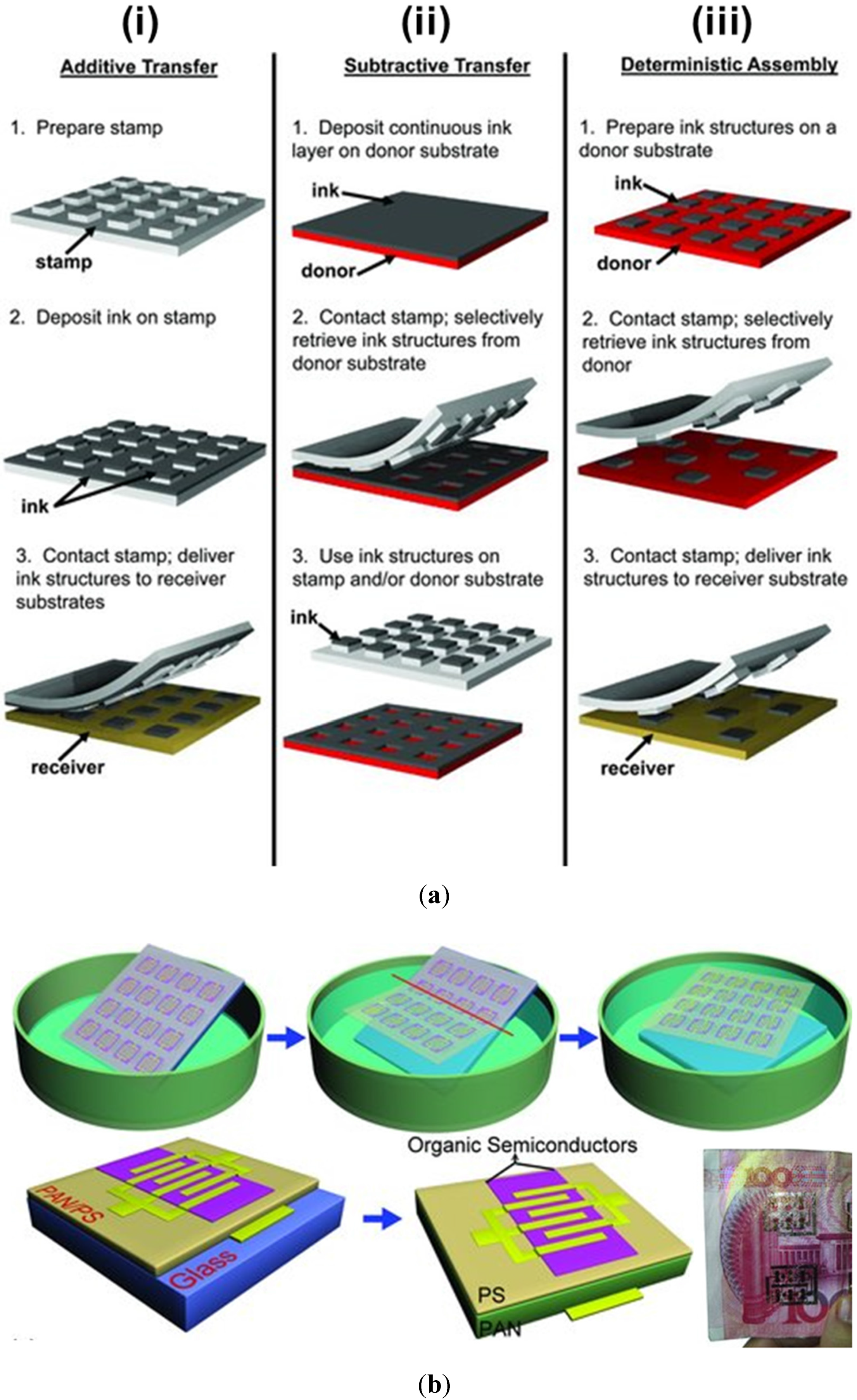
- Carlson, A.; Bowen, A.M.; Huang, Y.; Nuzzo, R.G.; Rogers, J.A. Transfer printing techniques for materials assembly and micro/nanodevice fabrication. Adv. Mater. 2012, 24, 5284–5318. [Google Scholar] [CrossRef] [PubMed]
- Stauth, S.A.; Parviz, B.A. Self-assembled single-crystal silicon circuits on plastic. Proc. Natl. Acad. Sci. USA 2006, 103, 13922–13927. [Google Scholar] [CrossRef] [PubMed]
- Kim, T.-I.; Jung, Y.H.; Chung, H.-J.; Yu, K.J.; Ahmed, N.; Corcoran, C.J.; Park, J.S.; Jin, S.H.; Rogers, J.A. Deterministic assembly of releasable single crystal silicon-metal oxide field-effect devices formed from bulk wafers. Appl. Phys. Lett. 2013, 102, 182104. [Google Scholar] [CrossRef]
- Lee, C.H.; Kim, D.R.; Zheng, X. Fabricating nanowire devices on diverse substrates by simple transfer-printing methods. Proc. Natl. Acad. Sci. USA 2010, 107, 9950–9955. [Google Scholar] [CrossRef] [PubMed]
- Kim, S.; Jeong, H.Y.; Kim, S.K.; Choi, S.-Y.; Lee, K.J. Flexible memristive memory array on plastic substrates. Nano Lett. 2011, 11, 5438–5442. [Google Scholar] [CrossRef] [PubMed]
- Sevilla, G.A.T.; Rojas, J.P.; Fahad, H.M.; Hussain, A.M.; Ghanem, R.; Smith, C.E.; Hussain, M.M. Flexible and Transparent Silicon-on-Polymer Based Sub-20 nm Non-planar 3D FinFET for Brain-Architecture Inspired Computation. Adv. Mater. 2014, 26, 2794–2799. [Google Scholar] [CrossRef] [PubMed]
- Liang, L.; Li, K.; Xiao, C.; Fan, S.; Liu, J.; Zhang, W.; Xu, W.; Tong, W.; Liao, J.; Zhou, Y. Vacancy Associates-rich Ultrathin Nanosheets for High Performance and Flexible Nonvolatile Memory Device. J. Am. Chem. Soc. 2015, 137, 3102–3108. [Google Scholar] [CrossRef] [PubMed]
- Zhang, L.; Wang, H.; Zhao, Y.; Guo, Y.; Hu, W.; Yu, G.; Liu, Y. Substrate-free ultra-flexible organic field-effect transistors and five-stage ring oscillators. Adv. Mater. 2013, 25, 5455–5460. [Google Scholar] [CrossRef] [PubMed]
- Kang, B.; Lee, W.H.; Cho, K. Recent advances in organic transistor printing processes. ACS Appl. Mater. Interfaces 2013, 5, 2302–2315. [Google Scholar] [CrossRef] [PubMed]
- Kim, S.; Son, J.H.; Lee, S.H.; You, B.K.; Park, K.I.; Lee, H.K.; Byun, M.; Lee, K.J. Flexible Crossbar-Structured Resistive Memory Arrays on Plastic Substrates via Inorganic-Based Laser Lift-Off. Adv. Mater. 2014, 26, 7480–7487. [Google Scholar] [CrossRef] [PubMed]
- Wang, G.; Raji, A.-R.O.; Lee, J.-H.; Tour, J.M. Conducting-Interlayer SiOx Memory Devices on Rigid and Flexible Substrates. ACS Nano 2014, 8, 1410–1418. [Google Scholar] [CrossRef] [PubMed]
- Lin, C.; Su, C.; Chang, C.; Wu, H. Resistive Switching Behavior of Al/Al2O3/ZrO2/Al Structural Device for Flexible Nonvolatile Memory Application. IEEE Trans. Magn. 2014, 50, 1–4. [Google Scholar]
- Hota, M.; Bera, M.; Maiti, C. Flexible metal–insulator–metal capacitors on polyethylene terephthalate plastic substrates. Semicond. Sci. Technol. 2012, 27, 105001. [Google Scholar] [CrossRef]
- Hagendorfer, H.; Lienau, K.; Nishiwaki, S.; Fella, C.M.; Kranz, L.; Uhl, A.R.; Jaeger, D.; Luo, L.; Gretener, C.; Buecheler, S. Highly transparent and conductive ZnO: Al thin films from a low temperature aqueous solution approach. Adv. Mater. 2014, 26, 632–636. [Google Scholar] [CrossRef] [PubMed]
- Shahrjerdi, D.; Bedell, S.W. Extremely flexible nanoscale ultrathin body silicon integrated circuits on plastic. Nano Lett. 2012, 13, 315–320. [Google Scholar] [CrossRef] [PubMed]
- Stephen, W.B.; Keith, F.; Paul, L.; Davood, S.; John, A.O.; Devendra, S. Layer transfer by controlled spalling. J. Phys. D: Appl. Phys. 2013, 46, 152002. [Google Scholar]
- Bellanger, P.; Serra, J. Room Temperature Spalling of Thin Silicon Foils Using a Kerfless Technique. Energy Procedia 2014, 55, 873–878. [Google Scholar] [CrossRef]
- Rojas, J.P.; Ghoneim, M.T.; Young, C.D.; Hussain, M.M. Flexible High-/Metal Gate Metal/Insulator/Metal Capacitors on Silicon (100) Fabric. IEEE Trans. Electron. Devices 2013, 60, 3305–3309. [Google Scholar] [CrossRef]
- Rojas, J.P.; Sevilla, G.T.; Hussain, M.M. Structural and electrical characteristics of high-k/metal gate metal oxide semiconductor capacitors fabricated on flexible, semi-transparent silicon (100) fabric. Appl. Phys. Lett. 2013, 102, 064102. [Google Scholar] [CrossRef]
- Nassar, J.M.; Hussain, A.M.; Rojas, J.P.; Hussain, M.M. Low-cost high-quality crystalline germanium based flexible devices. Phys. Status Solidi RRL 2014, 8, 794–800. [Google Scholar] [CrossRef]
- Sevilla, G.A.T.; Inayat, S.B.; Rojas, J.P.; Hussain, A.M.; Hussain, M.M. Flexible and Semi-Transparent Thermoelectric Energy Harvesters from Low Cost Bulk Silicon (100). Small 2013, 9, 3916–3921. [Google Scholar] [CrossRef] [PubMed]
- Rojas, J.P.; Torres Sevilla, G.A.; Ghoneim, M.T.; Inayat, S.B.; Ahmed, S.M.; Hussain, A.M.; Hussain, M.M. Transformational Silicon Electronics. ACS Nano 2014, 8, 1468–1474. [Google Scholar] [CrossRef] [PubMed]
- Torres Sevilla, G.A.; Ghoneim, M.T.; Fahad, H.; Rojas, J.P.; Hussain, A.M.; Hussain, M.M. Flexible Nanoscale High-Performance FinFETs. ACS Nano 2014, 8, 9850–9856. [Google Scholar] [CrossRef] [PubMed]
- Wang, S.; Pu, J.; Chan, D.S.H.; Cho, B.J.; Loh, K.P. Wide memory window in graphene oxide charge storage nodes. Appl. Phys. Lett. 2010, 96, 143109. [Google Scholar] [CrossRef]
- Liu, J.; Yin, Z.; Cao, X.; Zhao, F.; Wang, L.; Huang, W.; Zhang, H. Fabrication of Flexible, All-Reduced Graphene Oxide Non-Volatile Memory Devices. Adv. Mater. 2013, 25, 233–238. [Google Scholar] [CrossRef] [PubMed]
- Sohn, J.I.; Choi, S.S.; Morris, S.M.; Bendall, J.S.; Coles, H.J.; Hong, W.-K.; Jo, G.; Lee, T.; Welland, M.E. Novel Nonvolatile Memory with Multibit Storage Based on a ZnO Nanowire Transistor. Nano Lett. 2010, 10, 4316–4320. [Google Scholar] [CrossRef] [PubMed]
- Hong, A.J.; Song, E.B.; Yu, H.S.; Allen, M.J.; Kim, J.; Fowler, J.D.; Wassei, J.K.; Park, Y.; Wang, Y.; Zou, J.; et al. Graphene Flash Memory. ACS Nano 2011, 5, 7812–7817. [Google Scholar] [CrossRef] [PubMed]
- Bertolazzi, S.; Krasnozhon, D.; Kis, A. Nonvolatile Memory Cells Based on MoS2/Graphene Heterostructures. ACS Nano 2013, 7, 3246–3252. [Google Scholar] [CrossRef] [PubMed]
- Casula, G.; Cosseddu, P.; Busby, Y.; Pireaux, J.-J.; Rosowski, M.; Tkacz Szczesna, B.; Soliwoda, K.; Celichowski, G.; Grobelny, J.; Novák, J.; et al. Air-stable, non-volatile resistive memory based on hybrid organic/inorganic nanocomposites. Org. Electron. 2015, 18, 17–23. [Google Scholar] [CrossRef]
- Chung, A.; Jamal, D.; Jeong-Soo, L.; Meyyappan, M. Nanoscale memory devices. Nanotechnology 2010, 21, 412001. [Google Scholar] [CrossRef] [PubMed]
- Makarov, A.; Sverdlov, V.; Selberherr, S. Emerging memory technologies: Trends, challenges, and modeling methods. Microelectron. Reliab. 2012, 52, 628–634. [Google Scholar] [CrossRef]
- Wang, L.; Yang, C.; Wen, J.; Gai, S. Emerging nonvolatile memories to go beyond scaling limits of conventional CMOS nanodevices. J. Nanomater. 2014, 2014, 927696. [Google Scholar] [CrossRef]
- Naber, R.C.G.; Asadi, K.; Blom, P.W.M.; de Leeuw, D.M.; de Boer, B. Organic nonvolatile memory devices based on ferroelectricity. Adv. Mater. 2010, 22, 933–945. [Google Scholar] [CrossRef] [PubMed]
- Wang, H.; Peng, Y.Q.; Ji, Z.Y.; Liu, M.; Shang, L.W.; Liu, X.H. Nonvolatile memory devices based on organic field-effect transistors. Chin. Sci. Bul. 2011, 56, 1325–1332. [Google Scholar] [CrossRef]
- Liu, X.; Ji, Z.Y.; Liu, M.; Shang, L.W.; Li, D.M.; Dai, Y.H. Advancements in organic nonvolatile memory devices. Chin. Sci. Bull. 2011, 56, 3178–3190. [Google Scholar] [CrossRef]
- Chou, Y.H.; Chang, H.C.; Liu, C.L.; Chen, W.C. Polymeric charge storage electrets for non-volatile organic field effect transistor memory devices. Polym. Chem. 2015, 6, 341–352. [Google Scholar] [CrossRef]
- Lee, J.S. Review paper: Nano-floating gate memory devices. Electron. Mater. Lett. 2011, 7, 175–183. [Google Scholar] [CrossRef]
- Lee, T.; Chen, Y. Organic resistive nonvolatile memory materials. MRS Bull. 2012, 37, 144–149. [Google Scholar] [CrossRef]
- Jeong, D.S.; Thomas, R.; Katiyar, R.S.; Scott, J.F.; Kohlstedt, H.; Petraru, A.; Hwang, C.S. Emerging memories: Resistive switching mechanisms and current status. Rep. Prog. Phys. 2012, 75, 076502. [Google Scholar] [CrossRef] [PubMed]
- Panda, D.; Tseng, T.Y. Perovskite oxides as resistive switching memories: A review. Ferroelectrics 2014, 471, 23–64. [Google Scholar] [CrossRef]
- Lin, W.P.; Liu, S.J.; Gong, T.; Zhao, Q.; Huang, W. Polymer-based resistive memory materials and devices. Adv. Mater. 2014, 26, 570–606. [Google Scholar] [CrossRef] [PubMed]
- Porro, S.; Accornero, E.; Pirri, C.F.; Ricciardi, C. Memristive devices based on graphene oxide. Carbon 2015, 85, 383–396. [Google Scholar] [CrossRef]
- Seok, J.Y.; Song, S.J.; Yoon, J.H.; Yoon, K.J.; Park, T.H.; Kwon, D.E.; Lim, H.; Kim, G.H.; Jeong, D.S.; Hwang, C.S. A review of three-dimensional resistive switching cross-bar array memories from the integration and materials property points of view. Adv. Funct. Mater. 2014, 24, 5316–5339. [Google Scholar] [CrossRef]
- Kim, T.W.; Yang, Y.; Li, F.; Kwan, W.L. Electrical memory devices based on inorganic/organic nanocomposites. NPG Asia Mater. 2012, 4, e18. [Google Scholar] [CrossRef]
- Liu, X.; Liu, Y.; Chen, W.; Li, J.; Liao, L. Ferroelectric memory based on nanostructures. Nanoscale Res. Lett. 2012, 7, 285. [Google Scholar] [CrossRef] [PubMed]
- Mai, M.; Ke, S.; Lin, P.; Zeng, X. Ferroelectric polymer thin films for organic electronics. J. Nanomaterials 2015, 2015, 812538. [Google Scholar] [CrossRef]
- Kurosawa, T.; Higashihara, T.; Ueda, M. Polyimide memory: A pithy guideline for future applications. Polym. Chem. 2013, 4, 16–30. [Google Scholar] [CrossRef]
- Han, S.-T.; Zhou, Y.; Roy, V.A.L. Towards the Development of Flexible Non-Volatile Memories. Adv. Mater. 2013, 25, 5425–5449. [Google Scholar] [CrossRef] [PubMed]
- Acharyya, D.; Hazra, A.; Bhattacharyya, P. A journey towards reliability improvement of TiO2 based Resistive Random Access Memory: A review. Microelectron. Reliab. 2014, 54, 541–560. [Google Scholar] [CrossRef]
- Gale, E. TiO2-based memristors and ReRAM: Materials, mechanisms and models (a review). Semicond. Sci. Technol. 2014, 29, 104004. [Google Scholar] [CrossRef]
- Zhou, Y.; Han, S.-T.; Sonar, P.; Roy, V.A.L. Nonvolatile multilevel data storage memory device from controlled ambipolar charge trapping mechanism. Sci. Rep. 2013, 3, 2319. [Google Scholar] [CrossRef] [PubMed]
- Kim, S.-J.; Lee, J.-S. Flexible organic transistor memory devices. Nano Lett. 2010, 10, 2884–2890. [Google Scholar] [CrossRef] [PubMed]
- Ye, Z.; Su-Ting, H.; Zong-Xiang, X.; Roy, V.A.L. Low voltage flexible nonvolatile memory with gold nanoparticles embedded in poly(methyl methacrylate). Nanotechnology 2012, 23, 344014. [Google Scholar]
- Li, J.; Yan, F. Solution-Processable Low-Voltage and Flexible Floating-Gate Memories Based on an n-Type Polymer Semiconductor and High-k Polymer Gate Dielectrics. ACS Appl. Mater. Interfaces 2014, 6, 12815–12820. [Google Scholar] [CrossRef] [PubMed]
- Kim, S.-J.; Song, J.-M.; Lee, J.-S. Transparent organic thin-film transistors and nonvolatile memory devices fabricated on flexible plastic substrates. J. Mater. Chem. 2011, 21, 14516–14522. [Google Scholar] [CrossRef]
- Zhang, X.; Xie, H.; Liu, Z.; Tan, C.; Luo, Z.; Li, H.; Lin, J.; Sun, L.; Chen, W.; Xu, Z. Black phosphorus quantum dots. Angew. Chem. Int. Ed. 2015, 54, 3653–3657. [Google Scholar] [CrossRef] [PubMed]
- Dung, M.X.; Choi, J.-K.; Jeong, H.-D. Newly Synthesized Silicon Quantum Dot–Polystyrene Nanocomposite Having Thermally Robust Positive Charge Trapping. ACS Appl. Mater. Interfaces 2013, 5, 2400–2409. [Google Scholar] [CrossRef] [PubMed]
- Jeon, Y.; Lee, M.; Moon, T.; Kim, S. Flexible Nano-Floating-Gate Memory With Channels of Enhancement-Mode Si Nanowires. IEEE Trans. Electron Devices 2012, 59, 2939–2942. [Google Scholar] [CrossRef]
- Hwang, S.K.; Lee, J.M.; Kim, S.; Park, J.S.; Park, H.I.; Ahn, C.W.; Lee, K.J.; Lee, T.; Kim, S.O. Flexible Multilevel Resistive Memory with Controlled Charge Trap B- and N-Doped Carbon Nanotubes. Nano Lett. 2012, 12, 2217–2221. [Google Scholar] [CrossRef] [PubMed]
- Yu, W.J.; Chae, S.H.; Lee, S.Y.; Duong, D.L.; Lee, Y.H. Ultra-Transparent, Flexible Single-walled Carbon Nanotube Non-volatile Memory Device with an Oxygen-decorated Graphene Electrode. Adv. Mater. 2011, 23, 1889–1893. [Google Scholar] [CrossRef] [PubMed]
- Tsai, C.-L.; Xiong, F.; Pop, E.; Shim, M. Resistive Random Access Memory Enabled by Carbon Nanotube Crossbar Electrodes. ACS Nano 2013, 7, 5360–5366. [Google Scholar] [CrossRef] [PubMed]
- Lee, W.; Kahya, O.; Toh, C.T.; Özyilmaz, B.; Ahn, J.-H. Flexible graphene–PZT ferroelectric nonvolatile memory. Nanotechnology 2013, 24, 475202. [Google Scholar] [CrossRef] [PubMed]
- Kim, S.M.; Song, E.B.; Lee, S.; Zhu, J.; Seo, D.H.; Mecklenburg, M.; Seo, S.; Wang, K.L. Transparent and flexible graphene charge-trap memory. ACS Nano 2012, 6, 7879–7884. [Google Scholar] [CrossRef] [PubMed]
- Hong, S.K.; Kim, J.-E.; Kim, S.O.; Jin Cho, B. Non-volatile memory using graphene oxide for flexible electronics. In Proceedings of the 2010 10th IEEE Conference on Nanotechnology (IEEE-NANO), Seoul, Korea, 17–20 August 2010; pp. 604–606.
- Jeong, H.Y.; Kim, J.Y.; Kim, J.W.; Hwang, J.O.; Kim, J.-E.; Lee, J.Y.; Yoon, T.H.; Cho, B.J.; Kim, S.O.; Ruoff, R.S. Graphene oxide thin films for flexible nonvolatile memory applications. Nano Lett. 2010, 10, 4381–4386. [Google Scholar] [CrossRef] [PubMed]
- Kafy, A.; Sadasivuni, K.K.; Kim, H.C.; Akther, A.; Kim, J. Designing flexible energy and memory storage materials using cellulose modified graphene oxide nanocomposites. Phys. Chem. Chem. Phys. 2015. [Google Scholar] [CrossRef] [PubMed]
- Li, R.; Sun, R.; Sun, Y.; Gao, P.; Zhang, Y.; Zeng, Z.; Li, Q. Towards formation of fibrous woven memory devices from all-carbon electronic fibers. Phys. Chem. Chem. Phys. 2015, 17, 7104–7108. [Google Scholar] [PubMed]
- An, B.W.; Kim, K.; Kim, M.; Kim, S.-Y.; Hur, S.-H.; Park, J.-U. Direct Printing of Reduced Graphene Oxide on Planar or Highly Curved Surfaces with High Resolutions Using Electrohydrodynamics. Small 2015, 11, 2263–2268. [Google Scholar] [CrossRef] [PubMed]
- Seo, S.; Yoon, Y.; Lee, J.; Park, Y.; Lee, H. Nitrogen-Doped Partially Reduced Graphene Oxide Rewritable Nonvolatile Memory. ACS Nano 2013, 7, 3607–3615. [Google Scholar] [CrossRef] [PubMed]
- Zhang, E.; Wang, W.; Zhang, C.; Jin, Y.; Zhu, G.; Sun, Q.; Zhang, D.W.; Zhou, P.; Xiu, F. Tunable Charge-Trap Memory Based on Few-Layer MoS2. ACS Nano 2015, 9, 612–619. [Google Scholar] [CrossRef] [PubMed]
- Forrest, S.R. The path to ubiquitous and low-cost organic electronic appliances on plastic. Nature 2004, 428, 911–918. [Google Scholar] [CrossRef] [PubMed]
- Reuss, R.H.; Chalamala, B.R.; Moussessian, A.; Kane, M.G.; Kumar, A.; Zhang, D.C.; Rogers, J.A.; Hatalis, M.; Temple, D.; Moddel, G.; et al. Macroelectronics: Perspectives on Technology and Applications. Proc. IEEE 2005, 93, 1239–1256. [Google Scholar] [CrossRef]
- Lumelsky, V.J.; Shur, M.S.; Wagner, S. Sensitive skin. IEEE Sens. J. 2001, 1, 41–51. [Google Scholar] [CrossRef]
- Ricker, T. Sony's rollable OLED display can wrap around a pencil, our hearts (video). AOL Tech., 2010. Available online: http://www.engadget.com/2010/05/26/sonys-rollable-oled-display-can-wrap-around-a-pencil-our-heart/ (accessed on 22 June 2015).
- Skillings, J. Samsung shows off Youm flexible display. CBS Interactive Inc., 2013. Available online: http://www.cnet.com/news/sprint-puts-cramming-behind-it-with-50-million-settlement/ (accessed on 22 June 2015).
- De Boeck, J. IoT: The Impact of things. In Proceedings of the Symposium on Very Large Scale Integration, Digest of Technical Papers, Kyoto, Japan, 15–18 June 2015; pp. T82–T83.
- Takenaka, T.; Inoue, H.; Hosomi, T.; Nakamura, Y. FPGA-accelerated Complex Event Processing. In Proceedings of the Symposium on Very Large Scale Integration, Digest of Technical Papers, Kyoto, Japan, 15–18 June 2015; pp. C126–C127.
- Yamauchi, T.; Kondo, H.; Nii, K. Automotive Low Power Technology for IoT Society. In Proceedings of the Symposium on Very Large Scale Integration, Digest of Technical Papers, Kyoto, Japan, 15–18 June 2015; pp. T80–T81.
- Yano, K.; Akitomi, T.; Ara, K.; Watanabe, J.; Tsuji, S.; Sato, N.; Hayakawa, M.; Moriwaki, N. Profiting From IoT: The Key Is Very-Large-Scale Happiness Integration. In Proceedings of the Symposium on Very Large Scale Integration, Digest of Technical Papers, Kyoto, Japan, 15–18 June 2015; pp. C24–C27.
- Turnquist, M.; Hiienkari, M.; Mäkipää, J.; Jevtic, R.; Pohjalainen, E.; Kallio, T.; Koskinen, L. Fully Integrated DC-DC Converter and a 0.4V 32-bit CPU with Timing-Error Prevention Supplied from a Prototype 1.55V Li-ion Battery. In Proceedings of the Symposium on Very Large Scale Integration, Digest of Technical Papers, Kyoto, Japan, 15–18 June 2015; pp. C320–C321.
- Yamamoto, Y.; Makiyama, H.; Yamashita, T.; Oda, H.; Kamohara, S. Novel Single p+Poly-Si/Hf/SiON Gate Stack Technology on Silicon-on-Thin-Buried-Oxide (SOTB) for Ultra-Low Leakage Applications. In Proceedings of the Symposium on Very Large Scale Integration, Digest of Technical Papers, Kyoto, Japan, 15–18 June 2015; pp. T170–T171.
- Lee, A.; Chang, M.-F.; Lin, C.-C.; Chen, C.-F.; Ho, M.-S.; Kuo, C.-C.; Tseng, P.-L.; Sheu, S.-S.; Ku, T.-K. RRAM-based 7T1R Nonvolatile SRAM with 2x Reduction in Store Energy and 94x Reduction in Restore Energy for Frequent-Off Instant-On Applications. In Proceedings of the Symposium on Very Large Scale Integration, Digest of Technical Papers, Kyoto, Japan, 15–18 June 2015; pp. C76–C77.
- Kobayashi, M.; Hiramoto, T. Device Design Guideline for Steep Slope Ferroelectric FET Using Negative Capacitance in Sub-0.2V Operation: Operation Speed, Material Requirement and Energy Efficiency. In Proceedings of the Symposium on Very Large Scale Integration, Digest of Technical Papers, Kyoto, Japan, 15–18 June 2015; pp. T212–T213.
- Steegen, A. Technology innovation in an IoT Era. In Proceedings of the Symposium on Very Large Scale Integration, Digest of Technical Papers, Kyoto, Japan, 15–18 June 2015; pp. C170–C171.
- Aitken, R.; Chandra, V.; Myers, J.; Sandhu, B.; Shifren, L.; Yeric, G. Device and technology implications of the Internet of Things. In Proceedings of the Symposium on Very Large Scale Integration, Digest of Technical Papers, Honolulu, HI, USA, 9–12 June 2014; pp. 1–4.
- Ueki, M.; Takeuchi, K.; Yamamoto, T.; Tanabe, A.; Ikarashi, N.; Saitoh, M.; Nagumo, T.; Sunamura, H.; Narihiro, M.; Uejima, K.; et al. Low-Power Embedded ReRAM Technology for IoT Applications. In Proceedings of the Symposium on Very Large Scale Integration, Digest of Technical Papers, Kyoto, Japan, 15–18 June 2015; pp. T108–T109.
- Whatmough, P.-N.; Smart, G.; Das, D.; Andreopoulos, Y.; Bull, D.M. A 0.6V All-Digital Body-Coupled Wakeup Transceiver for IoT Applications. In Proceedings of the Symposium on Very Large Scale Integration, Digest of Technical Papers, Kyoto, Japan, 15–18 June 2015; pp. C98–C99.
- Tanakamaru, S.; Yamazawa, H.; Takeuchi, K. Privacy-Protection Solid-State Storage (PP-SSS) System: Automatic Lifetime Management of Internet-Data’s Right to be Forgotten. In Proceedings of the Symposium on Very Large Scale Integration, Digest of Technical Papers, Kyoto, Japan, 15–18 June 2015; pp. C130–C131.
- Antonio, C.; Barrera, C. Flexible microstrip antennas. Proc. SPIE 2013, 8730, 873009. [Google Scholar]
- Ahmed, S.; Tahir, F.A.; Shamim, A.; Cheema, H.M. A Compact Kapton-based Inkjet Printed Multiband Antenna for Flexible Wireless Devices. IEEE Antenn. Wirel. PR. 2015. [Google Scholar] [CrossRef]
- Inui, T.; Koga, H.; Nogi, M.; Komoda, N.; Suganuma, K. A Miniaturized Flexible Antenna Printed on a High Dielectric Constant Nanopaper Composite. Adv. Mater. 2015, 27, 1112–1116. [Google Scholar] [CrossRef] [PubMed]
- Nicolas, T.; Philippe, C.; Ronan, S.; Vincent, S.; Hiroyuki, F. Polydimethylsiloxane membranes for millimeter-wave planar ultra flexible antennas. J. Micromech. Microeng. 2006, 16, 2389. [Google Scholar]
- Khaleel, H.R.; Al-Rizzo, H.M.; Rucker, D.G. Compact Polyimide-Based Antennas for Flexible Displays. J. Display Technol. 2012, 8, 91–97. [Google Scholar] [CrossRef]
- Garg, D.P.; Anderson, G.L. Research in active composite materials and structures: An overview. Proc. SPIE 2000, 3992, 2–12. [Google Scholar]
- Li, J.; Zhao, Y.; Tan, H.S.; Guo, Y.; Di, C.-A.; Yu, G.; Liu, Y.; Lin, M.; Lim, S.H.; Zhou, Y. A stable solution-processed polymer semiconductor with record high-mobility for printed transistors. Sci. Rep. 2012, 2, 754. [Google Scholar] [CrossRef] [PubMed]
- Kang, I.; Yun, H.-J.; Chung, D.S.; Kwon, S.-K.; Kim, Y.-H. Record high hole mobility in polymer semiconductors via side-chain engineering. J. Am. Chem. Soc. 2013, 135, 14896–14899. [Google Scholar] [CrossRef] [PubMed]
- Caraveo-Frescas, J.; Khan, M.; Alshareef, H. Polymer ferroelectric field-effect memory device with SnO channel layer exhibits record hole mobility. Sci. Rep. 2014, 4, 5243. [Google Scholar] [CrossRef] [PubMed]
- Min, S.-Y.; Kim, T.-S.; Kim, B.J.; Cho, H.; Noh, Y.-Y.; Yang, H.; Cho, J.H.; Lee, T.-W. Large-scale organic nanowire lithography and electronics. Nat. Commun. 2013, 4, 1773. [Google Scholar] [CrossRef] [PubMed]
- Yuan, Y.; Giri, G.; Ayzner, A.L.; Zoombelt, A.P.; Mannsfeld, S.C.; Chen, J.; Nordlund, D.; Toney, M.F.; Huang, J.; Bao, Z. Ultra-high mobility transparent organic thin film transistors grown by an off-centre spin-coating method. Nat. Commun. 2014, 5, 3005. [Google Scholar] [CrossRef] [PubMed]
- Yang, Y.; Yang, H.; Yang, M.; Shen, G.; Yu, R. Amperometric glucose biosensor based on a surface treated nanoporous ZrO2/chitosan composite film as immobilization matrix. Anal. Chim. Acta 2004, 525, 213–220. [Google Scholar] [CrossRef]
- Kim, S.H.; Hong, K.; Xie, W.; Lee, K.H.; Zhang, S.; Lodge, T.P.; Frisbie, C.D. Electrolyte-Gated Transistors for Organic and Printed Electronics. Adv. Mater. 2013, 25, 1822–1846. [Google Scholar] [CrossRef] [PubMed]
- Oh, C.H.; Shin, H.J.; Nam, W.J.; Ahn, B.C.; Cha, S.Y.; Yeo, S.D. 21.1: Invited Paper: Technological Progress and Commercialization of OLED TV. Dig. Tech. Pap. - Soc. Inf. Disp. Int. Symp. 2013, 44, 239–242. [Google Scholar] [CrossRef]
- Zhai, Y.; Mathew, L.; Rao, R.; Xu, D.; Banerjee, S.K. High-performance flexible thin-film transistors exfoliated from bulk wafer. Nano Lett. 2012, 12, 5609–5615. [Google Scholar] [CrossRef] [PubMed]
- Shahrjerdi, D.; Bedell, S.; Khakifirooz, A.; Fogel, K.; Lauro, P.; Cheng, K.; Ott, J.; Gaynes, M.; Sadana, D. Advanced flexible CMOS integrated circuits on plastic enabled by controlled spalling technology. In Proceedings of the IEEE International Electron Devices Meeting, San Francisco, CA, USA, 10–13 December 2012; pp. 5.1.1–5.1.4.
- Murray, C.E.; Saenger, K.; Kalenci, O.; Polvino, S.; Noyan, I.; Lai, B.; Cai, Z. Submicron mapping of silicon-on-insulator strain distributions induced by stressed liner structures. J. Appl. Phys. 2008, 104, 013530:1–013530:8. [Google Scholar] [CrossRef]
- Hu, S. Film-edge-induced stress in substrates. J. Appl. Phys. 1979, 50, 4661–4666. [Google Scholar] [CrossRef]
- Bedell, S.W.; Shahrjerdi, D.; Hekmatshoar, B.; Fogel, K.; Lauro, P.A.; Ott, J.A.; Sosa, N.; Sadana, D. Kerf-less removal of Si, Ge, and III–V layers by controlled spalling to enable low-cost PV technologies. IEEE J. Photovolt. 2012, 2, 141–147. [Google Scholar] [CrossRef]
- Ghoneim, M.T.; Rojas, J.P.; Hussain, A.M.; Hussain, M.M. Additive advantage in characteristics of MIMCAPs on flexible silicon (100) fabric with release-first process. Phys. Status Solidi RRL 2014, 8, 163–166. [Google Scholar] [CrossRef]
- Seo, J.; Han, K.; Youn, T.; Heo, H.-E.; Jang, S.; Kim, J.; Yoo, H.; Hwang, J.; Yang, C.; Lee, H. Highly reliable M1X MLC NAND flash memory cell with novel active air-gap and p+ poly process integration technologies. In Proceedings of the IEEE International Electron Devices Meeting, Technical Digest, Washington, DC, USA, 9–11 December 2013; pp. 3.6.1–3.6.4.
- Ghoneim, M.T.; Fahad, H.M.; Rojas, J.P.; Torres Sevilla, G.A.; Alfaraj, N.; Lizardo, E.B.; Hussain, M.M. Self-Cooling in Ultra-thin Mono-Crystalline Silicon by Nostril Architecture Inspired Porous Network of Embedded Micro-Air Channels. 2015; (unpublished). [Google Scholar]
- Takahashi, K.; Terao, H.; Tomita, Y.; Yamaji, Y.; Hoshino, M.; Sato, T.; Morifuji, T.; Sunohara, M.; Bonkohara, M. Current status of research and development for three-dimensional chip stack technology. Jpn. J. Appl. Phys. 2001, 40, 3032. [Google Scholar] [CrossRef]
- Gao, S.; Dong, Z.; Kang, R.; Zhang, B.; Guo, D. Warping of silicon wafers subjected to back-grinding process. Precis. Eng. 2015, 40, 87–93. [Google Scholar] [CrossRef]
- Jeon, E.-B.; Park, J.-D.; Song, J.H.; Lee, H.J.; Kim, H.-S. Bi-axial fracture strength characteristic of an ultra-thin flash memory chip. J. Micromech. Microeng. 2012, 22, 105014. [Google Scholar] [CrossRef]
- Sekhar, V.N.; Shen, L.; Kumar, A.; Chai, T.C.; Zhang, X.; Premchandran, C.; Kripesh, V.; Yoon, S.W.; Lau, J.H. Study on the Effect of Wafer Back Grinding Process on Nanomechanical Behavior of Multilayered Low-K Stack. IEEE Trans. Compon. Packag. Manuf. Technol. 2012, 2, 3–12. [Google Scholar] [CrossRef]
- Lu, S.-T.; Chen, W.-H. Reliability and flexibility of ultra-thin chip-on-flex (UTCOF) interconnects with anisotropic conductive adhesive (ACA) joints. IEEE Trans. Adv. Packag. 2010, 33, 702–712. [Google Scholar]
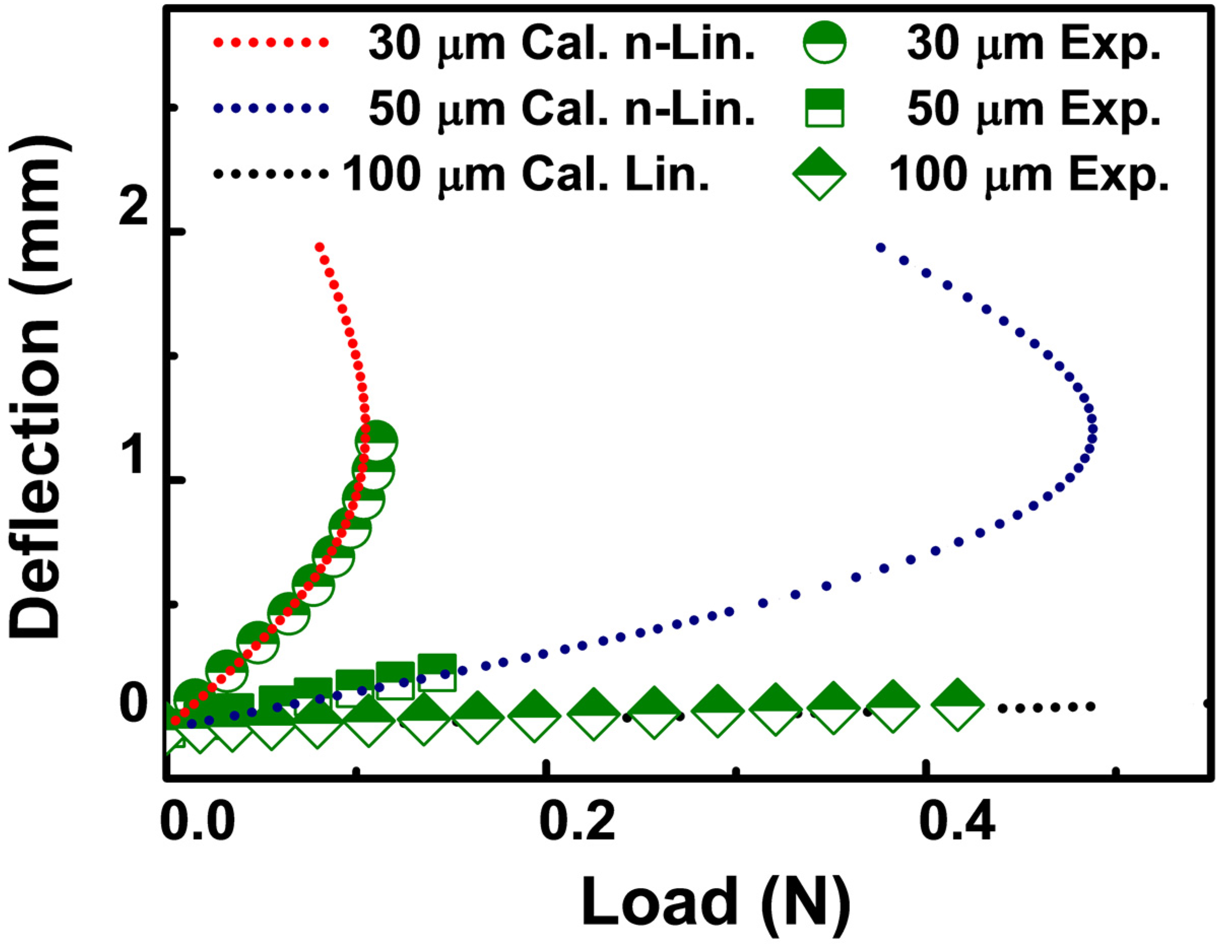
- Liu, Z.; Huang, Y.; Xiao, L.; Tang, P.; Yin, Z. Nonlinear characteristics in fracture strength test of ultrathin silicon die. Semicond. Sci. Technol. 2015, 30, 045005. [Google Scholar] [CrossRef]
- Paul, I.; Majeed, B.; Razeeb, K.; Barton, J. Statistical fracture modelling of silicon with varying thickness. Acta Mater. 2006, 54, 3991–4000. [Google Scholar] [CrossRef]
- Wu, J.; Huang, C.; Liao, C. Fracture strength characterization and failure analysis of silicon dies. Microelectron. Reliab. 2003, 43, 269–277. [Google Scholar] [CrossRef]
- Boyd, E.J.; Uttamchandani, D. Measurement of the Anisotropy of Young's Modulus in Single-Crystal Silicon. J. Microelectromech. Syst. 2012, 21, 243–249. [Google Scholar] [CrossRef]
- Committee, I.R. International Technology Roadmap for Semiconductors: 2013 Edition Executive Summary. Semiconductor Industry Association: San Francisco, CA. Available online: http://public.itrs.net/ITRS%201999-2014%20Mtgs,%20Presentations%20&%20Links/2013ITRS/2013Chapters/2013ExecutiveSummary.pdf (accessed on 1 June 2015).
- Govoreanu, B.; Kar, G.; Chen, Y.; Paraschiv, V.; Kubicek, S.; Fantini, A.; Radu, I.; Goux, L.; Clima, S.; Degraeve, R. 10× 10nm2 Hf/HfOx crossbar resistive RAM with excellent performance, reliability and low-energy operation. In Proceedings of the IEEE International Electron Device Meeting, Washington, DC, USA, 5–7 December 2011; pp. 31.6.1–31.6.4.
- Jo, S.H.; Chang, T.; Ebong, I.; Bhadviya, B.B.; Mazumder, P.; Lu, W. Nanoscale memristor device as synapse in neuromorphic systems. Nano Lett. 2010, 10, 1297–1301. [Google Scholar] [CrossRef] [PubMed]
- Strukov, D.B.; Snider, G.S.; Stewart, D.R.; Williams, R.S. The missing memristor found. Nature 2008, 453, 80–83. [Google Scholar] [CrossRef] [PubMed]
- Chua, L.O. Memristor-the missing circuit element. IEEE Trans. Circuit Theory 1971, 18, 507–519. [Google Scholar] [CrossRef]
- Shannigrahi, S.R.; Jang, H.M. Fatigue-free lead zirconate titanate-based capacitors for nonvolatile memories. Appl. Phys. Lett. 2001, 79, 1051–1053. [Google Scholar] [CrossRef]
- Parkin, S.; Xin, J.; Kaiser, C.; Panchula, A.; Roche, K.; Samant, M. Magnetically engineered spintronic sensors and memory. Proc. IEEE 2003, 91, 661–680. [Google Scholar] [CrossRef]
- Gupta, M.K.; Hasan, M. Robust High Speed Ternary Magnetic Content Addressable Memory. IEEE Trans. Electron Devices 2015, 62, 1163–1169. [Google Scholar] [CrossRef]
- Lencer, D.; Salinga, M.; Wuttig, M. Design Rules for Phase-Change Materials in Data Storage Applications. Adv. Mater. 2011, 23, 2030–2058. [Google Scholar] [CrossRef] [PubMed]
- Yoon, J.M.; Shin, D.O.; Yin, Y.; Seo, H.K.; Kim, D.; Kim, Y.I.; Jin, J.H.; Kim, Y.T.; Bae, B.-S.; Kim, S.O. Fabrication of high-density In3Sb1Te2 phase change nanoarray on glass-fabric reinforced flexible substrate. Nanotechnology 2012, 23, 255301. [Google Scholar] [CrossRef] [PubMed]
- Yoon, K.; Il Han, P.; Seongjae, C.; Jang-Gn, Y.; Jung Hoon, L.; Doo-Hyun, K.; Gil Sung, L.; Se-Hwan, P.; Dong Hua, L.; Won Bo, S.; et al. A Vertical 4-Bit SONOS Flash Memory and a Unique 3-D Vertical Array Structure. IEEE Trans. Nanotechnol. 2010, 9, 70–77. [Google Scholar] [CrossRef]
- Lee, J.S.; Kim, Y.M.; Kwon, J.H.; Shin, H.; Sohn, B.H.; Lee, J. Tunable memory characteristics of nanostructured, nonvolatile charge trap memory devices based on a binary mixture of metal nanoparticles as a charge trapping layer. Adv. Mater. 2009, 21, 178–183. [Google Scholar] [CrossRef]
- Pott, V.; Vaddi, R.; Geng Li, C.; Lin, J.T.M.; Kim, T.T. Design Optimization of Pulsed-Mode Electromechanical Nonvolatile Memory. IEEE Electron Device Lett. 2012, 33, 1207–1209. [Google Scholar] [CrossRef]
- Young Choi, W.; Hei, K.; Lee, D.; Lai, J.; Tsu-Jae King, L. Compact Nano-Electro-Mechanical Non-Volatile Memory (NEMory) for 3D Integration. In Proceedings of the IEEE International Electron Devices Meeting, Washington, DC, USA, 10–12 December 2007; pp. 603–606.
- Green, J.E.; Choi, J.W.; Boukai, A.; Bunimovich, Y.; Johnston-Halperin, E.; DeIonno, E.; Luo, Y.; Sheriff, B.A.; Xu, K.; Shin, Y.S. A 160-kilobit molecular electronic memory patterned at 1011 bits per square centimetre. Nature 2007, 445, 414–417. [Google Scholar] [CrossRef] [PubMed]
- Joachim, H.O.; Jacob, M.; Rehm, N. 2T2C Signal Margin Test Mode Using a Defined Charge Exchange between BL and/BL. U.S. Patent US6876590 B2, 5 April 2005. [Google Scholar]
- Wang, X.P.; Fang, Z.; Li, X.; Chen, B.; Gao, B.; Kang, J.F.; Chen, Z.X.; Kamath, A.; Shen, N.S.; Singh, N.; et al. Highly compact 1T-1R architecture (4F2 footprint) involving fully CMOS compatible vertical GAA nano-pillar transistors and oxide-based RRAM cells exhibiting excellent NVM properties and ultra-low power operation. In Proceedings of the IEEE International Electron Devices Meeting, San Francisco, CA, USA, 10–13 December 2012; pp. 20.6.1–20.6.4.
- Joachim, H.O.; Jacob, M.; Rehm, N. 2T2C Signal Margin Test Mode Using a Defined Charge Exchange between BL and/BL. U.S. Patent US20040095821 A1, 20 May 2004. [Google Scholar]
- Ogasawara, S.; Ishiwara, H. Fabrication and characterization of 1T2C-type ferroelectric memory cell with local interconnections. Jpn. J. Appl. Phys. 2002, 41, 6895. [Google Scholar] [CrossRef]
- Hyun-Soo, K.; Shuu'ichirou, Y.; Toru, I.; Takaaki, F.; Hiroshi, O.; Hiroshi, I. Fabrication and Characterization of 1 k-bit 1T2C-Type Ferroelectric Memory Cell Array. Jpn. J. Appl. Phys. 2005, 44, 2715. [Google Scholar]
- Hyun-Soo, K.; Shuu'ichirou, Y.; Hiroshi, I. Improved Data Disturbance Effects in 1T2C-Type Ferroelectric Memory Array. Jpn. J. Appl. Phys. 2004, 43, 2558. [Google Scholar]
- Micheloni, R.; Campardo, G.; Olivo, P. Memories in Wireless Systems; Springer Science & Business Media: Berlin-Heidelberg, Germany, 2008; pp. 40–43. [Google Scholar]
- Hatano, K.; Chida, A.; Okano, T.; Sugisawa, N.; Inoue, T.; Seo, S.; Suzuki, K.; Oikawa, Y.; Miyake, H.; Koyama, J. 3.4-Inch Quarter High Definition Flexible Active Matrix Organic Light Emitting Display with Oxide Thin Film Transistor. Jpn. J. Appl. Phys. 2011, 50, 03CC06. [Google Scholar] [CrossRef]
- Wang, Z.R.; Xin, J.Z.; Ren, X.C.; Wang, X.L.; Leung, C.W.; Shi, S.Q.; Ruotolo, A.; Chan, P.K.L. Low power flexible organic thin film transistors with amorphous Ba0.7Sr0.3TiO3 gate dielectric grown by pulsed laser deposition at low temperature. Org. Electron. 2012, 13, 1223–1228. [Google Scholar] [CrossRef]
- Tsai, L.-W.; Tai, N.-H. Enhancing the Electrical Properties of a Flexible Transparent Graphene-Based Field-Effect Transistor Using Electropolished Copper Foil for Graphene Growth. ACS Appl. Mater. Interfaces 2014, 6, 10489–10496. [Google Scholar] [CrossRef] [PubMed]
- Sekitani, T.; Zschieschang, U.; Klauk, H.; Someya, T. Flexible organic transistors and circuits with extreme bending stability. Nat. Mater. 2010, 9, 1015–1022. [Google Scholar] [CrossRef] [PubMed]
- Yi, M.; Guo, Y.; Guo, J.; Yang, T.; Chai, Y.; Fan, Q.; Xie, L.; Huang, W. The mechanical bending effect and mechanism of high performance and low-voltage flexible organic thin-film transistors with a cross-linked PVP dielectric layer. J. Mater. Chem. C 2014, 2, 2998–3004. [Google Scholar] [CrossRef]
- Lau, P.H.; Takei, K.; Wang, C.; Ju, Y.; Kim, J.; Yu, Z.; Takahashi, T.; Cho, G.; Javey, A. Fully Printed, High Performance Carbon Nanotube Thin-Film Transistors on Flexible Substrates. Nano Lett. 2013, 13, 3864–3869. [Google Scholar] [CrossRef] [PubMed]
- Nigam, A.; Schwabegger, G.; Ullah, M.; Ahmed, R.; Fishchuk, I.I.; Kadashchuk, A.; Simbrunner, C.; Sitter, H.; Premaratne, M.; Ramgopal Rao, V. Strain induced anisotropic effect on electron mobility in C60 based organic field effect transistors. Appl. Phys. Lett. 2012, 101, 083305. [Google Scholar] [CrossRef]
- Yi, H.T.; Payne, M.M.; Anthony, J.E.; Podzorov, V. Ultra-flexible solution-processed organic field-effect transistors. Nat. Commun. 2012, 3, 1259. [Google Scholar] [CrossRef] [PubMed]
- Inoue, A.; Okamoto, T.; Sakai, M.; Kuniyoshi, S.; Yamauchi, H.; Nakamura, M.; Kudo, K. Flexible organic field-effect transistor fabricated by thermal press process. Phys. Status Solidi A 2013, 210, 1353–1357. [Google Scholar] [CrossRef]
- Sakai, M.; Okamoto, T.; Yamazaki, Y.; Hayashi, J.; Yamaguchi, S.; Kuniyoshi, S.; Yamauchi, H.; Sadamitsu, Y.; Hamada, M.; Kudo, K. Organic thin-film transistor fabricated between flexible films by thermal lamination. Phys. Status Solidi RRL 2013, 7, 1093–1096. [Google Scholar] [CrossRef]
- Cao, X.; Chen, H.; Gu, X.; Liu, B.; Wang, W.; Cao, Y.; Wu, F.; Zhou, C. Screen Printing as a Scalable and Low-Cost Approach for Rigid and Flexible Thin-Film Transistors Using Separated Carbon Nanotubes. ACS Nano 2014, 8, 12769–12776. [Google Scholar] [CrossRef] [PubMed]
- Fan, C.-L.; Lin, W.-C.; Peng, H.-H.; Lin, Y.-Z.; Huang, B.-R. Correlation between ambient air and continuous bending stress for the electrical reliability of flexible pentacene-based thin-film transistors. Jpn. J. Appl. Phys. 2015, 54, 011602. [Google Scholar] [CrossRef]
- Ribierre, J.C.; Watanabe, S.; Matsumoto, M.; Muto, T.; Aoyama, T. Majority carrier type conversion in solution-processed organic transistors and flexible complementary logic circuits. Appl. Phys. Lett. 2010, 96, 083303. [Google Scholar] [CrossRef]
- Fukuda, K.; Minamiki, T.; Minami, T.; Watanabe, M.; Fukuda, T.; Kumaki, D.; Tokito, S. Printed Organic Transistors with Uniform Electrical Performance and Their Application to Amplifiers in Biosensors. Adv. Electron. Mater. 2015, 1, 1400052. [Google Scholar] [CrossRef]
- Werkmeister, F.; Nickel, B. Towards flexible organic thin film transistors (OTFTs) for biosensing. J. Mater. Chem. B 2013, 1, 3830–3835. [Google Scholar] [CrossRef]
- Hu, Y.; Warwick, C.; Sou, A.; Jiang, L.; Sirringhaus, H. Fabrication of ultra-flexible, ultra-thin organic field-effect transistors and circuits by a peeling-off method. J. Mater. Chem. C 2014, 2, 1260–1263. [Google Scholar] [CrossRef]
- Salvatore, G.A.; Münzenrieder, N.; Barraud, C.; Petti, L.; Zysset, C.; Büthe, L.; Ensslin, K.; Tröster, G. Fabrication and Transfer of Flexible Few-Layers MoS2 Thin Film Transistors to Any Arbitrary Substrate. ACS Nano 2013, 7, 8809–8815. [Google Scholar] [CrossRef] [PubMed]
- Xu, H.; Pang, J.; Xu, M.; Li, M.; Guo, Y.; Chen, Z.; Wang, L.; Zou, J.; Tao, H.; Wang, L. Fabrication of Flexible Amorphous Indium-Gallium-Zinc-Oxide Thin-Film Transistors by a Chemical Vapor Deposition-Free Process on Polyethylene Napthalate. ECS J. Solid State Sci. Technol. 2014, 3, Q3035–Q3039. [Google Scholar] [CrossRef]
- Hwang, B.-U.; Kim, D.-I.; Cho, S.-W.; Yun, M.-G.; Kim, H.J.; Kim, Y.J.; Cho, H.-K.; Lee, N.-E. Role of ultrathin Al2O3 layer in organic/inorganic hybrid gate dielectrics for flexibility improvement of InGaZnO thin film transistors. Org. Electron. 2014, 15, 1458–1464. [Google Scholar] [CrossRef]
- Deng, W.; Zhang, X.; Wang, J.; Shang, Q.; Gong, C.; Zhang, X.; Zhang, Q.; Jie, J. Very facile fabrication of aligned organic nanowires based high-performance top-gate transistors on flexible, transparent substrate. Org. Electron. 2014, 15, 1317–1323. [Google Scholar] [CrossRef]
- Park, C.B.; Kim, K.M.; Lee, J.E.; Na, H.; Yoo, S.S.; Yang, M.S. Flexible electrophoretic display driven by solution-processed organic TFT with highly stable bending feature. Org. Electron. 2014, 15, 3538–3545. [Google Scholar] [CrossRef]
- Kinkeldei, T.; Munzenrieder, N.; Zysset, C.; Cherenack, K.; Tröster, G. Encapsulation for Flexible Electronic Devices. IEEE Electron Device Lett. 2011, 32, 1743–1745. [Google Scholar] [CrossRef]
- Min Hee, C.; Byung Soon, K.; Jin, J. High-Performance Flexible TFT Circuits Using TIPS Pentacene and Polymer Blend on Plastic. IEEE Electron Device Lett. 2012, 33, 1571–1573. [Google Scholar]
- Zysset, C.; Munzenrieder, N.; Petti, L.; Buthe, L.; Salvatore, G.A.; Troster, G. IGZO TFT-Based All-Enhancement Operational Amplifier Bent to a Radius of 5 mm. IEEE Electron Device Lett. 2013, 34, 1394–1396. [Google Scholar] [CrossRef]
- Wee, D.; Yoo, S.; Kang, Y.H.; Kim, Y.H.; Ka, J.-W.; Cho, S.Y.; Lee, C.; Ryu, J.; Yi, M.H.; Jang, K.-S. Poly (imide-benzoxazole) gate insulators with high thermal resistance for solution-processed flexible indium-zinc oxide thin-film transistors. J. Mater. Chem. C 2014, 2, 6395–6401. [Google Scholar] [CrossRef]
- Mativenga, M.; Geng, D.; Kim, B.-S.; Jang, J. Fully-Transparent and Rollable Electronics. ACS Appl. Mater. Interfaces 2014, 7, 1578–1585. [Google Scholar] [CrossRef] [PubMed]
- Li, H.U.; Jackson, T.N. Oxide Semiconductor Thin Film Transistors on Thin Solution-Cast Flexible Substrates. IEEE Electron Device Lett. 2015, 36, 35–37. [Google Scholar] [CrossRef]
- Park, J.H.; Oh, J.Y.; Han, S.W.; Lee, T.I.; Baik, H.K. Low-Temperature, Solution-Processed ZrO2: B Thin Film: A Bifunctional Inorganic/Organic Interfacial Glue for Flexible Thin-Film Transistors. ACS Appl. Mater. Interfaces 2015, 7, 4494–4503. [Google Scholar] [CrossRef] [PubMed]
- Yu, X.; Zeng, L.; Zhou, N.; Guo, P.; Shi, F.; Buchholz, D.B.; Ma, Q.; Yu, J.; Dravid, V.P.; Chang, R.P.H.; et al. Ultra-Flexible, “Invisible” Thin-Film Transistors Enabled by Amorphous Metal Oxide/Polymer Channel Layer Blends. Adv. Mater. 2015, 27, 2390–2399. [Google Scholar] [CrossRef] [PubMed]
- Chang, H.-Y.; Yang, S.; Lee, J.; Tao, L.; Hwang, W.-S.; Jena, D.; Lu, N.; Akinwande, D. High-Performance, Highly Bendable MoS2 Transistors with High-K Dielectrics for Flexible Low-Power Systems. ACS Nano 2013, 7, 5446–5452. [Google Scholar] [CrossRef] [PubMed]
- Rojas, J.P.; Torres Sevilla, G.A.; Hussain, M.M. Can We Build a Truly High Performance Computer Which is Flexible and Transparent? Sci. Rep. 2013, 3, 2609. [Google Scholar] [CrossRef] [PubMed]
- Shahrjerdi, D.; Bedell, S.W.; Khakifirooz, A.; Fogel, K.; Lauro, P.; Cheng, K.; Ott, J.A.; Gaynes, M.; Sadana, D.K. Advanced flexible CMOS integrated circuits on plastic enabled by controlled spalling technology. In Proceedings of the International Electron Devices Meeting, San Francisco, CA, USA, 10–13 December 2012; pp. 5.1.1–5.1.4.
- Ghoneim, M.T.; Rojas, J.P.; Young, C.D.; Bersuker, G.; Hussain, M.M. Electrical Analysis of High Dielectric Constant Insulator and Metal Gate Metal Oxide Semiconductor Capacitors on Flexible Bulk Mono-Crystalline Silicon. IEEE Trans. Rel. 2014, 64, 579–585. [Google Scholar] [CrossRef]
- Ghoneim, M.; Kutbee, A.; Nasseri, F.G.; Bersuker, G.; Hussain, M. Mechanical anomaly impact on metal-oxide-semiconductor capacitors on flexible silicon fabric. Appl. Phys. Lett. 2014, 104, 234104. [Google Scholar] [CrossRef]
- International Technology Roadmap for Semiconductors: 2011 Edition Executive Summary. Semiconductor Industry Association: San Francisco, CA. Available online: http://www.itrs.net/ITRS%201999-2014%20Mtgs,%20Presentations%20&%20Links/2011ITRS/2011Chapters/2011ExecSum.pdf (accessed on 1 June 2015).
- Zidan, M.A.; Eltawil, A.M.; Kurdahi, F.; Fahmy, H.A.; Salama, K.N. Memristor Multiport Readout: A Closed-Form Solution for Sneak Paths. IEEE Trans. Nanotechnol. 2014, 13, 274–282. [Google Scholar] [CrossRef]
- Gorshkov, K.; Berzina, T.; Erokhin, V.; Fontana, M.P. Organic memristor based on the composite materials: Conducting and ionic polymers, gold nanoparticles and graphenes. Procedia Comput. Sci. 2011, 7, 248–249. [Google Scholar] [CrossRef]
- Pan, L.; Ji, Z.; Yi, X.; Zhu, X.; Chen, X.; Shang, J.; Liu, G.; Li, R.-W. Metal-Organic Framework Nanofilm for Mechanically Flexible Information Storage Applications. Adv. Funct. Mater. 2015, 25, 2677–2685. [Google Scholar] [CrossRef]
- Zhao, F.; Cheng, H.; Hu, Y.; Song, L.; Zhang, Z.; Jiang, L.; Qu, L. Functionalized Graphitic Carbon Nitride for Metal-free, Flexible and Rewritable Nonvolatile Memory Device via Direct Laser-Writing. Sci. Rep. 2014, 4, 5882. [Google Scholar] [CrossRef] [PubMed]
- Son, D.I.; Kim, T.W.; Shim, J.H.; Jung, J.H.; Lee, D.U.; Lee, J.M.; Park, W.I.; Choi, W.K. Flexible organic bistable devices based on graphene embedded in an insulating poly (methyl methacrylate) polymer layer. Nano Lett. 2010, 10, 2441–2447. [Google Scholar] [CrossRef] [PubMed]
- Yu, A.-D.; Kurosawa, T.; Lai, Y.-C.; Higashihara, T.; Ueda, M.; Liu, C.-L.; Chen, W.-C. Flexible polymer memory devices derived from triphenylamine–pyrene containing donor–acceptor polyimides. J. Mater. Chem. 2012, 22, 20754–20763. [Google Scholar] [CrossRef]
- Ji, Y.; Cho, B.; Song, S.; Kim, T.W.; Choe, M.; Kahng, Y.H.; Lee, T. Stable switching characteristics of organic nonvolatile memory on a bent flexible substrate. Adv. Mater. 2010, 22, 3071–3075. [Google Scholar] [CrossRef] [PubMed]
- GyunáYoo, H.; JaeáLee, K. Flexible one diode–one resistor resistive switching memory arrays on plastic substrates. R. Soc. Chem. Adv. 2014, 4, 20017–20023. [Google Scholar]
- Wu, C.; Zhang, K.; Wang, F.; Wei, X.; Zhao, J. Resistance Switching Characteristics of Sputtered Titanium Oxide on a Flexible Substrate. ECS Trans. 2012, 44, 87–91. [Google Scholar]
- Zou, S.; Michael, C. Flexible non-volatile Cu/CuxO/Ag ReRAM memory devices fabricated using ink-jet printing technology. In Proceedings of the IEEE 64th Electronic Components and Technology Conference, Orlando, FL, USA, 27–30 May 2014; pp. 441–446.
- Lin, C.-C.; Lin, H.-B. Resistive switching behavior of ZrO2 thin film fabricated on PES flexible substrate. In Proceedings of the IEEE International Conference on Electron Devices and Solid State Circuit, Bangkok, Thailand, 3–5 December 2012; pp. 1–2.
- Yao, J.; Lin, J.; Dai, Y.; Ruan, G.; Yan, Z.; Li, L.; Zhong, L.; Natelson, D.; Tour, J.M. Highly transparent nonvolatile resistive memory devices from silicon oxide and graphene. Nat. Commun. 2012, 3, 1101. [Google Scholar] [CrossRef] [PubMed]
- Liang, L.; Li, K.; Xiao, C.; Fan, S.; Liu, J.; Zhang, W.; Xu, W.; Tong, W.; Liao, J.; Zhou, Y.; et al. Vacancy Associates-Rich Ultrathin Nanosheets for High Performance and Flexible Nonvolatile Memory Device. J. Am. Chem. Soc. 2015, 137, 3102–3108. [Google Scholar] [CrossRef] [PubMed]
- Wu, S.-C.; Feng, H.-T.; Yu, M.-J.; Wang, I.-T.; Hou, T.-H. Flexible Three-Bit-Per-Cell Resistive Switching Memory Using a-IGZO TFTs. IEEE Electron Device Lett. 2013, 34, 1265–1267. [Google Scholar] [CrossRef]
- Mondal, S.; Chueh, C.-H.; Pan, T.-M. High-Performance Flexible ReRAM Device for Low-Power Nonvolatile Memory Applications. IEEE Electron Device Lett. 2013, 34, 1145–1147. [Google Scholar] [CrossRef]
- Jeong, H.Y.; Kim, Y.I.; Lee, J.Y.; Choi, S.-Y. A low-temperature-grown TiO2-based device for the flexible stacked RRAM application. Nanotechnology 2010, 21, 115203. [Google Scholar] [CrossRef] [PubMed]
- Gergel-Hackett, N.; Hamadani, B.; Dunlap, B.; Suehle, J.; Richter, C.; Hacker, C.; Gundlach, D. A flexible solution-processed memristor. IEEE Electron Device Lett. 2009, 30, 706–708. [Google Scholar] [CrossRef]
- Chou, K.; Cheng, C.; Zheng, Z.; Liu, M.; Chin, A. RRAM on Flexible Substrate With Excellent Resistance Distribution. IEEE Electron Device Lett. 2013, 34, 505–507. [Google Scholar] [CrossRef]
- Jang, J.; Pan, F.; Braam, K.; Subramanian, V. Resistance switching characteristics of solid electrolyte chalcogenide Ag2Se nanoparticles for flexible nonvolatile memory applications. Adv. Mater. 2012, 24, 3573–3576. [Google Scholar] [CrossRef] [PubMed]
- Ghoneim, M.T.; Zidan, M.A.; Salama, K.N.; Hussain, M.M. Towards neuromorphic electronics: Memristors on foldable silicon fabric. Microelectron. J. 2014, 45, 1392–1395. [Google Scholar] [CrossRef]
- Nagashima, K.; Koga, H.; Celano, U.; Zhuge, F.; Kanai, M.; Rahong, S.; Meng, G.; He, Y.; de Boeck, J.; Jurczak, M. Cellulose nanofiber paper as an ultra flexible nonvolatile memory. Sci. Rep. 2014, 4, 5532. [Google Scholar] [CrossRef] [PubMed]
- Waser, R.; Dittmann, R.; Staikov, G.; Szot, K. Redox-based resistive switching memories–nanoionic mechanisms, prospects, and challenges. Adv. Mater. 2009, 21, 2632–2663. [Google Scholar] [CrossRef]
- Lee, S.; Kim, H.; Jung, D.; Song, Y.; Jang, N.; Choi, M.; Jeon, B.; Lee, Y.; Lee, K.; Joo, S. Highly scalable sub-10F2 1T1C COB cell for high density FRAM. In Proceedings of the Symposium on Very Large Scale Integration, Digest of Technical Papers, Kyoto, Japan, 12–14 June 2001; pp. 111–112.
- Derbenwick, G.F.; Kamp, D.A.; Philpy, S.C.; Isaacson, A.F. Advances in FeRAM Technologies; Celis Semiconductor Corporation: Colorado, CO, USA, 2000. [Google Scholar]
- Eshita, T.; Wang, W.; Nakamura, K.; Mihara, S.; Saito, H.; Hikosaka, Y.; Inoue, K.; Kawashima, S.; Yamaguchi, H.; Nomura, K. Development of ferroelectric RAM (FRAM) for mass production. In Proceedings of the Joint IEEE International Symposium on the Applications of Ferroelectrics, International Workshop on Acoustic Transduction Materials and Devices & Workshop on Piezoresponse Force Microscopy, State College, PA, USA, 12–16 May 2014; pp. 1–3.
- Evans, J. Memory 101: What you need to know about FRAM, part 1: Embedding FeRAM. EETimes, 2014. Available online: http://www.eetimes.com/document.asp?doc_id=1280437&page_number=2 (accessed on 1 June 2015).
- Li, J.; Nagaraj, B.; Liang, H.; Cao, W.; Lee, C.H.; Ramesh, R. Ultrafast polarization switching in thin-film ferroelectrics. Appl. Phys. Lett. 2004, 84, 1174–1176. [Google Scholar] [CrossRef]
- Larsen, P.; Kampschoer, G.; van der Mark, M.; Klee, M. Ultrafast polarization switching of lead zirconate titanate thin films. In Proceedings of the 8th IEEE International Symposium on Applications of Ferroelectrics, Greenville, SC, USA, 30 August–2 September 1992; pp. 217–224.
- Shannigrahi, S.; Jang, H.M. Fatigue-free lead zirconate titanate-based capacitors for nonvolatile memories. Appl. Phys. Lett. 2001, 79, 1051–1053. [Google Scholar] [CrossRef]
- Nagel, N.; Bruchhaus, R.; Hornik, K.; Egger, U.; Zhuang, H.; Joachim, H.-O.; Rohr, T.; Beitel, G.; Ozaki, T.; Kunishima, I. New highly scalable 3 dimensional chain FeRAM cell with vertical capacitor. In Proceedings of the Symposium on Very Large Scale Integration Technology, Digest of Technical Papers, Honolulu, Hi, USA, 15–17 June 2004; pp. 146–147.
- Ghoneim, M.T.; Zidan, M.A.; Alnassar, M.Y.; Hanna, A.N.; Kosel, J.; Salama, K.N.; Hussain, M.M. Thin PZT-Based Ferroelectric Capacitors on Flexible Silicon for Nonvolatile Memory Applications. Adv. Electron. Mater. 2015, 1, 1500045. [Google Scholar] [CrossRef]
- Zuo, Z.; Chen, B.; Zhan, Q.-F.; Liu, Y.; Yang, H.; Li, Z.; Xu, G.; Li, R.-W. Preparation and ferroelectric properties of freestanding Pb (Zr, Ti) O3 thin membranes. J. Phys. D: Appl. Phys. 2012, 45, 185302. [Google Scholar] [CrossRef]
- Rho, J.; Kim, S.J.; Heo, W.; Lee, N.-E.; Lee, H.-S.; Ahn, J.-H. Ferroelectric Thin-Film Capacitors for Flexible Nonvolatile Memory Applications. IEEE Electron Device Lett. 2010, 31, 1017–1019. [Google Scholar] [CrossRef]
- Yoon, S.-M.; Yang, S.; Park, S.-H.K. Flexible Nonvolatile memory thin-film transistor using ferroelectric copolymer gate insulator and oxide semiconducting channel. J. Electrochem. Soc. 2011, 158, H892–H896. [Google Scholar] [CrossRef]
- Yoon, S.-M.; Yang, S.; Jung, S.-W.; Ko Park, S.-H.; Byun, C.-W.; Ryu, M.-K.; Oh, H.; Kim, K.; Hwang, C.-S.; Cho, K.-I. Organic/Inorganic Hybrid-Type Nonvolatile Memory Thin-Film Transistor on Plastic Substrate below 150 °C. Mater. Res. Soc. Symp. Proc. 2011, 1287. [Google Scholar] [CrossRef]
- Ghoneim, M.T.; Hussain, M.M. Study of harsh environment operation of flexible ferroelectric memory integrated with PZT and silicon fabric. Appl. Phys. Lett. 2015. (submitted). [Google Scholar]
- Kim, W.Y.; Lee, H.C. Stable Ferroelectric Poly (Vinylidene Fluoride-Trifluoroethylene) Film for Flexible Nonvolatile Memory Application. IEEE Electron Device Lett. 2012, 33, 260–262. [Google Scholar] [CrossRef]
- Bhansali, U.S.; Khan, M.; Alshareef, H. Organic ferroelectric memory devices with inkjet-printed polymer electrodes on flexible substrates. Microelectron. Eng. 2013, 105, 68–73. [Google Scholar] [CrossRef]
- Khan, M.; Bhansali, U.S.; Alshareef, H. Fabrication and characterization of all-polymer, transparent ferroelectric capacitors on flexible substrates. Org. Electron. 2011, 12, 2225–2229. [Google Scholar] [CrossRef]
- Yoon, S.-M.; Jung, S.-W.; Yang, S.; Park, S.-H.K.; Yu, B.-G.; Ishiwara, H. Bending characteristics of ferroelectric poly (vinylidene fluoride trifluoroethylene) capacitors fabricated on flexible polyethylene naphthalate substrate. Curr. Appl. Phys. 2011, 11, S219–S224. [Google Scholar] [CrossRef]
- Khan, M.; Bhansali, U.S.; Alshareef, H. High-Performance Non-Volatile Organic Ferroelectric Memory on Banknotes. Adv. Mater. 2012, 24, 2165–2170. [Google Scholar] [CrossRef] [PubMed]
- Song, Y.; Shen, Y.; Liu, H.; Lin, Y.; Li, M.; Nan, C.-W. Enhanced dielectric and ferroelectric properties induced by dopamine-modified BaTiO3 nanofibers in flexible poly (vinylidene fluoride-trifluoroethylene) nanocomposites. J. Mater. Chem. 2012, 22, 8063–8068. [Google Scholar] [CrossRef]
- Zhaoyue, L.; Tiansong, P.; Yaopeng, H.; Xiangjian, M.; Haisheng, X. Flexible ferroelectric polymer devices based on inkjet-printed electrodes from nanosilver ink. Nanotechnology 2015, 26, 055202. [Google Scholar]
- Jung, S.-W.; Choi, J.-S.; Koo, J.B.; Park, C.W.; Na, B.S.; Oh, J.-Y.; Lim, S.C.; Lee, S.S.; Chu, H.Y.; Yoon, S.-M. Flexible nonvolatile organic ferroelectric memory transistors fabricated on polydimethylsiloxane elastomer. Org. Electron. 2015, 16, 46–53. [Google Scholar] [CrossRef]
- Bae, I.; Hwang, S.K.; Kim, R.H.; Kang, S.J.; Park, C. Wafer-Scale Arrays of Nonvolatile Polymer Memories with Microprinted Semiconducting Small Molecule/Polymer Blends. ACS Appl. Mater. Interfaces 2013, 5, 10696–10704. [Google Scholar] [CrossRef] [PubMed]
- Takashima, D. Overview of ferams: Trends and perspectives. In Proceedings of the 11th Annual Non-Volatile Memory Technology Symposium, Shanghai, China, 7–9 November 2011; pp. 1–6.
- Ayguavives, F.; Agius, B.; Ea-Kim, B.; Vickridge, I. Oxygen transport during annealing of Pb (Zr, Ti) O3 thin films in O2 gas and its effect on their conductivity. J. Mater. Res. 2001, 16, 3005–3008. [Google Scholar] [CrossRef]
- Takashima, D.; Nagadomi, Y.; Ozaki, T. A 100 MHz Ladder FeRAM Design With Capacitance-Coupled-Bitline (CCB) Cell. IEEE J. Solid-State Circuits 2011, 46, 681–689. [Google Scholar] [CrossRef]
- Shiga, H.; Takashima, D.; Shiratake, S.; Hoya, K.; Miyakawa, T.; Ogiwara, R.; Fukuda, R.; Takizawa, R.; Hatsuda, K.; Matsuoka, F. A 1.6 GB/s DDR2 128 Mb chain FeRAM with scalable octal bitline and sensing schemes. IEEE J. Solid-State Circuits 2010, 45, 142–152. [Google Scholar] [CrossRef]
- Le Van, H.; Takahashi, M.; Sakai, S. Downsizing of Ferroelectric-Gate Field-Effect-Transistors for Ferroelectric-NAND Flash Memory Cells. In Proceedings of the 3rd IEEE International Memory Workshop, Monterey, CA, USA, 22–25 May 2011; pp. 1–4.
- International Technology Roadmap for Semiconductors: 2011 Edition Emerging Research Devices. Semiconductor Industry Association: San Francisco, CA. Available online: http://www.itrs.net/ITRS%201999–2014%20Mtgs,%20Presentations%20&%20Links/2011ITRS/2011Chapters/2011ERD.pdf (accessed on 1 June 2015).
- Rodriguez, J.; Rodriguez-Latorre, J.; Zhou, C.; Venugopal, A.; Acosta, A.; Ball, M.; Ndai, P.; Madan, S.; McAdams, H.; Udayakumar, K.R.; et al. 180nm FRAM reliability demonstration with ten years data retention at 125 °C. In Proceedings of the IEEE International Reliability Physics Symposium, Anaheim, CA, USA, 14–18 April 2013; pp. MY.11.11–MY.11.15.
- Udayakumar, K.R.; San, T.; Rodriguez, J.; Chevacharoenkul, S.; Frystak, D.; Rodriguez-Latorre, J.; Zhou, C.; Ball, M.; Ndai, P.; Madan, S.; et al. Low-power ferroelectric random access memory embedded in 180nm analog friendly CMOS technology. In Proceedings of the 5th IEEE International Memory Workshop, Monterey, CA, USA, 26–29 May 2013; pp. 128–131.
- Hong, S.-H.; Bae, B.-J.; Lee, H.; Jeong, J.-H. Fabrication of high density nano-pillar type phase change memory devices using flexible AAO shaped template. Microelectron. Eng. 2010, 87, 2081–2084. [Google Scholar] [CrossRef]
- Hong, S.-H.; Jeong, J.-H.; Kim, K.-I.; Lee, H. High density phase change data on flexible substrates by thermal curing type nanoimprint lithography. Microelectron. Eng. 2011, 88, 2013–2016. [Google Scholar] [CrossRef]
- Yoon, J.M.; Shin, D.O.; Yin, Y.; Seo, H.K.; Kim, D.; Kim, Y.I.; Jin, J.H.; Kim, Y.T.; Bae, B.-S.; Kim, S.O.; et al. Fabrication of high-density In 3 Sb 1 Te 2 phase change nanoarray on glass-fabric reinforced flexible substrate. Nanotechnology 2012, 23, 255301. [Google Scholar] [CrossRef] [PubMed]
- Mun, B.H.; You, B.K.; Yang, S.R.; Yoo, H.G.; Kim, J.M.; Park, W.I.; Yin, Y.; Byun, M.; Jung, Y.S.; Lee, K.J. Flexible One Diode-One Phase Change Memory Array Enabled by Block Copolymer Self-Assembly. ACS Nano 2015, 9, 4120–4128. [Google Scholar] [CrossRef] [PubMed]
- Han, S.-T.; Zhou, Y.; Wang, C.; He, L.; Zhang, W.; Roy, V.A.L. Layer-by-Layer-Assembled Reduced Graphene Oxide/Gold Nanoparticle Hybrid Double-Floating-Gate Structure for Low-Voltage Flexible Flash Memory. Adv. Mater. 2013, 25, 872–877. [Google Scholar] [CrossRef] [PubMed]
- Esaki, L. “Long journey into tunneling,” Les Prix Nobel en 1973. Imprimerie Royale PA, Norstedt Soner, Stockholm 1974, 46, 237–245. [Google Scholar]
- Eitan, B.; Frohman-Bentchkowsky, D. Hot-electron injection into the oxide in n-channel MOS devices. IEEE Trans. Electron Devices 1981, 28, 328–340. [Google Scholar] [CrossRef]
- Lee, J.-S.; Kim, Y.-M.; Kwon, J.-H.; Shin, H.; Sohn, B.-H.; Lee, J. Tunable Memory Characteristics of Nanostructured, Nonvolatile Charge Trap Memory Devices Based on a Binary Mixture of Metal Nanoparticles as a Charge Trapping Layer. Adv. Mater. 2009, 21, 178–183. [Google Scholar] [CrossRef]
- Zhou, Y.; Han, S.-T.; Xu, Z.-X.; Roy, V. Low voltage flexible nonvolatile memory with gold nanoparticles embedded in poly (methyl methacrylate). Nanotechnology 2012, 23, 344014. [Google Scholar] [CrossRef] [PubMed]
- Son, D.; Koo, J.H.; Song, J.-K.; Kim, J.; Lee, M.; Shim, H.J.; Park, M.; Lee, M.; Kim, J.H.; Kim, D.-H. Stretchable Carbon Nanotube Charge-Trap Floating-Gate Memory and Logic Devices for Wearable Electronics. ACS Nano 2015, 9, 5585–5593. [Google Scholar] [CrossRef] [PubMed]
- Han, K.S.; Park, Y.; Han, G.; Lee, B.H.; Lee, K.H.; Son, D.H.; Im, S.; Sung, M.M. Organic–inorganic nanohybrid nonvolatile memory transistors for flexible electronics. J. Mater. Chem. 2012, 22, 19007–19013. [Google Scholar] [CrossRef]
© 2015 by the authors; licensee MDPI, Basel, Switzerland. This article is an open access article distributed under the terms and conditions of the Creative Commons Attribution license (http://creativecommons.org/licenses/by/4.0/).
Share and Cite
Ghoneim, M.T.; Hussain, M.M. Review on Physically Flexible Nonvolatile Memory for Internet of Everything Electronics. Electronics 2015, 4, 424-479. https://0-doi-org.brum.beds.ac.uk/10.3390/electronics4030424
Ghoneim MT, Hussain MM. Review on Physically Flexible Nonvolatile Memory for Internet of Everything Electronics. Electronics. 2015; 4(3):424-479. https://0-doi-org.brum.beds.ac.uk/10.3390/electronics4030424
Chicago/Turabian StyleGhoneim, Mohamed T., and Muhammad M. Hussain. 2015. "Review on Physically Flexible Nonvolatile Memory for Internet of Everything Electronics" Electronics 4, no. 3: 424-479. https://0-doi-org.brum.beds.ac.uk/10.3390/electronics4030424