
Remote System Update for System on Programmable Chip Based on Controller Area Network

School of Physical Science and Technology, Southwest Jiaotong University, Chengdu 610031, China
*
Author to whom correspondence should be addressed.
Electronics 2017, 6(2), 45; https://0-doi-org.brum.beds.ac.uk/10.3390/electronics6020045
Submission received: 28 March 2017
/
Revised: 5 June 2017
/
Accepted: 9 June 2017
/
Published: 13 June 2017
(This article belongs to the Special Issue Hardware and Architecture)
Abstract
:In some application domains, using a download cable to update the system on a programmable chip (SoPC) is infeasible, which reduces the maintainability and flexibility of the system. Hence the remote system update (RSU) scheme is being studied. In this scheme, the serial configuration (EPCS) device involves a factory mode configuration image, which acts as the baseline, and an application mode configuration image, which is used for some specific functions. Specifically, a new application mode image is delivered through the controller area network (CAN) with the improved application layer protocol. Besides, the data flow and data check for transmitting a new image are constructed to combine the transmission reliability with efficiency. The boot sequence copying hardware configuration code and software configuration code is analyzed, and the advanced boot loader is carried out to specify boot address of the application mode image manually. Experiments have demonstrated the feasibility of updating and running a new application mode image, as well as rolling back into the factory mode image when no application mode image is available. This scheme applies a single CAN bus, which makes the system easy to construct and suitable for the field distributed control system.

1. Introduction
SoPC is a kind of embedded system that based on the field programmable gate arrays (FPGA). It has many merits, such as the rich hardware resource, flexible function, as well as the low project cost, and thus, it is widely used in automation, power electronics, and microwave [1,2,3,4]. Nevertheless, in some occasions, such as the satellite borne equipment, underwater equipment, and core printed circuit boards that are located in the cumbersome electromagnetism shields, connection via the download cable between the SoPC and computer is infeasible. It brings about great trouble when the equipment breaks down or new function is wanted. Thus, the maintainability and flexibility of the system are reduced. Therefore, remote system update (RSU) for programmable devices via the communication system has become a research hotspot [5,6,7,8].
Up to now, there have been a lot of successful cases of RSU for micro control units (MCU) [9,10,11], digital signal processers (DSP) [11,12,13], FPGA/SoPC [13,14,15,16,17], as well as advanced RISC machines (ARM) [18]. Besides, the communication channels in those researches include General Packet Radio Service (GPRS), Bluetooth, Peripheral Component Interconnect (PCI), Ethernet, RS-422, as well as CAN bus. Moreover, defending the configuration image from any kind of attacks is another important research item [19,20], especially for the wireless RSU. Furthermore, minimizing the new configuration image and memory occupation are of great importance when the system power dissipation limit is critical [21].
Nevertheless, most researchers chose to erase the total configuration device and then write a new configuration image in the RSU process. Once any accident occurs in the RSU process, SoPC will never start up for there is no practicable configuration image in the configuration devices. In order to fix this problem, some research makes use of several hardware or software configuration files. One acts as a baseline that is not allowed to be modified, while others act as updates [22,23,24]. A controller switches among them. If the update is not effective, the baseline will provide the basic function so as to keep the system working. However, there are few studies trying to update the whole SoPC configuration image with hardware and software in a single process.
In terms of the industry field control systems, CAN has the advantages in such aspects as message integrity, transmission distance, as well as interface cost. In [12,17], there’s a root board receiving new configuration image at first, which then sends it to other boards through another bus. This topology makes the system complex. Besides, a CAN data frame only contains eight bytes, but the medium scale SoPC configuration image is more than one megabyte (MB). Therefore, it takes the mass frames to send the total image. In order to reduce the risk of communication failure, [12] checks every data frame. It is no doubt that this will cost a lot of time when dealing with a large configuration image, which leads to the prolix and inconvenient application in the RSU process.
In terms of the RSU scheme that is planned in this article, the EPCS device contains two integrated SoPC configuration images. One is the application mode image for the expected functions. The other is the factory mode image, which updates the application mode image remotely and acts as the baseline. The dedicated RSU circuit that is provided by Altera will choose from the above two images for the purpose of loading. Even if the RSU process goes wrong, the system can roll back to the factory mode and request a new RSU process.
Both the factory mode image and application mode image own an embedded CAN controller intellectual property core (IP). Therefore, every node can receive RSU frames independently. Since the entire system adopts a single CAN bus, the system topology is succinct, easy to use, and suitable for the field distributed control system. In order to adapt to the various mission demands, CAN application layer protocol is optimized by dividing the identifiers and data field into several segments and every segment is entrusted with definite meaning. Besides, in order to give considerations to both sides of communication reality and efficiency, the data check of a new image is applied whenever the data buffer of an EPCS block is full, and also, the writing operation to the EPCS devices must be executed to the entire block.
An integrated SoPC configuration images includes a hardware part that is tightly followed by the software part. They are aligned to the same reference address, which is 0x00 by default. It leads to an address dislocation to the software part of the application mode image, because the application mode image is actually aligned to its header, and at the same time, the RSU dedicated circuit can merely correct the reference address for the hardware part. Therefore, an advanced boot loader is designed to specify where the software part of the application mode image locates, making the whole application mode image operational.
Experiments have been performed so as to verify the practicability of the RSU scheme by means of using a target SoPC with the factory mode image that is stored in EPCS device. A new application mode image with the experiment phenomenon that is different from the factory mode image is sent through CAN, and then saved in the EPCS device following the factory mode image. After triggering a reconfiguration, phenomenon of the new application mode image will take place. As a result, the application mode image has been updated.
2. Materials and Methods
2.1. Overall Design of RSU
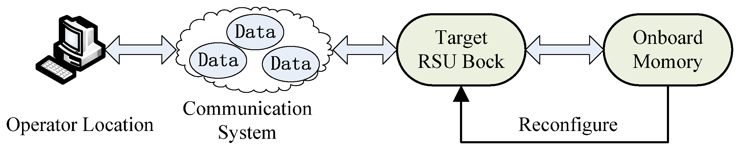
Generally speaking, RSU is a process, in which the operator will send a new configuration image through some communication systems to the target, and trigger the reconfiguration of the target by means of using the new configuration image, as demonstrated in Figure 1.
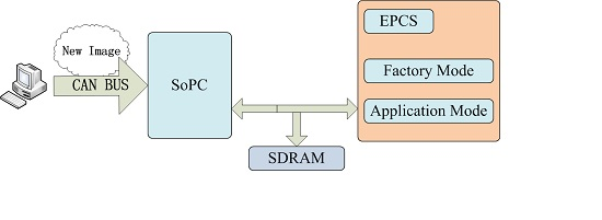
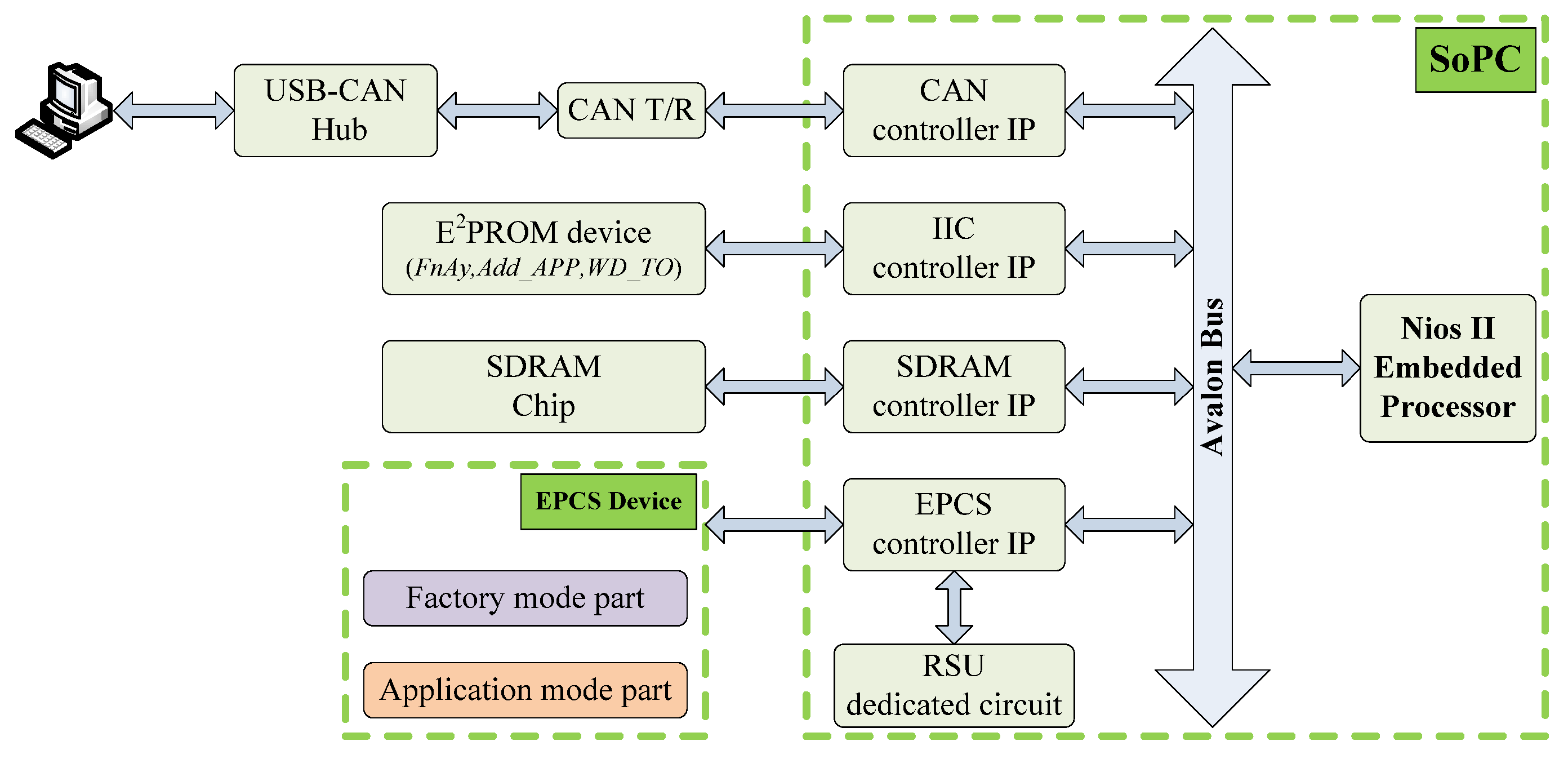
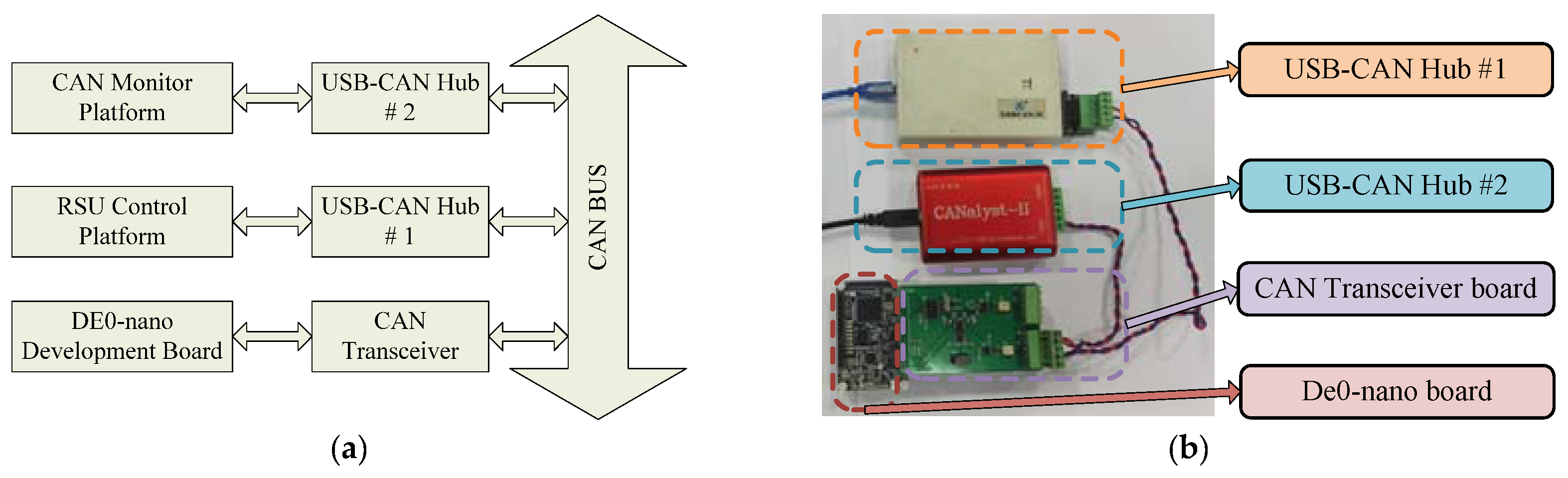
The proposed RSU scheme is made up of a host computer (upper computer, UC), a USB-CAN hub, an onboard CAN transceiver, a target SoPC (lower computer, LC) working in active serial (AS) programming mode, a piece of electrically erasable read-only memory (E2PROM), a piece of onboard synchronous dynamic random-access memory (SDRAM), as well as the EPCS device. The connection among them is demonstrated in Figure 2.
The target SoPC is based on the Nios II embedded softcore processor, and connected with the RSU dedicated circuit, which can be activated in Quartus II and other peripheral controller IPs so as to operate the corresponding peripherals. The EPCS device stores the factory mode and the application mode configuration image. Besides, the RSU dedicated circuit handles the whole configuration process of SoPC.E2PROM stores some parameters for RSU, such as FnAy that indicates whether to load application mode, Add_APP that represents the location of application mode configuration image and WD_TO that indicates RSU watchdog timer time out value. Moreover, the application programs and data run in the SDRAM. UC will first convert the SoPC hardware configuration file (*.sof) and software configuration file (*.elf) into the EPCS programming files (*.flash), and then merges them into a complete SoPC configuration image. After that, the UC will transmit the new application mode image by means of the USB-CAN hub.
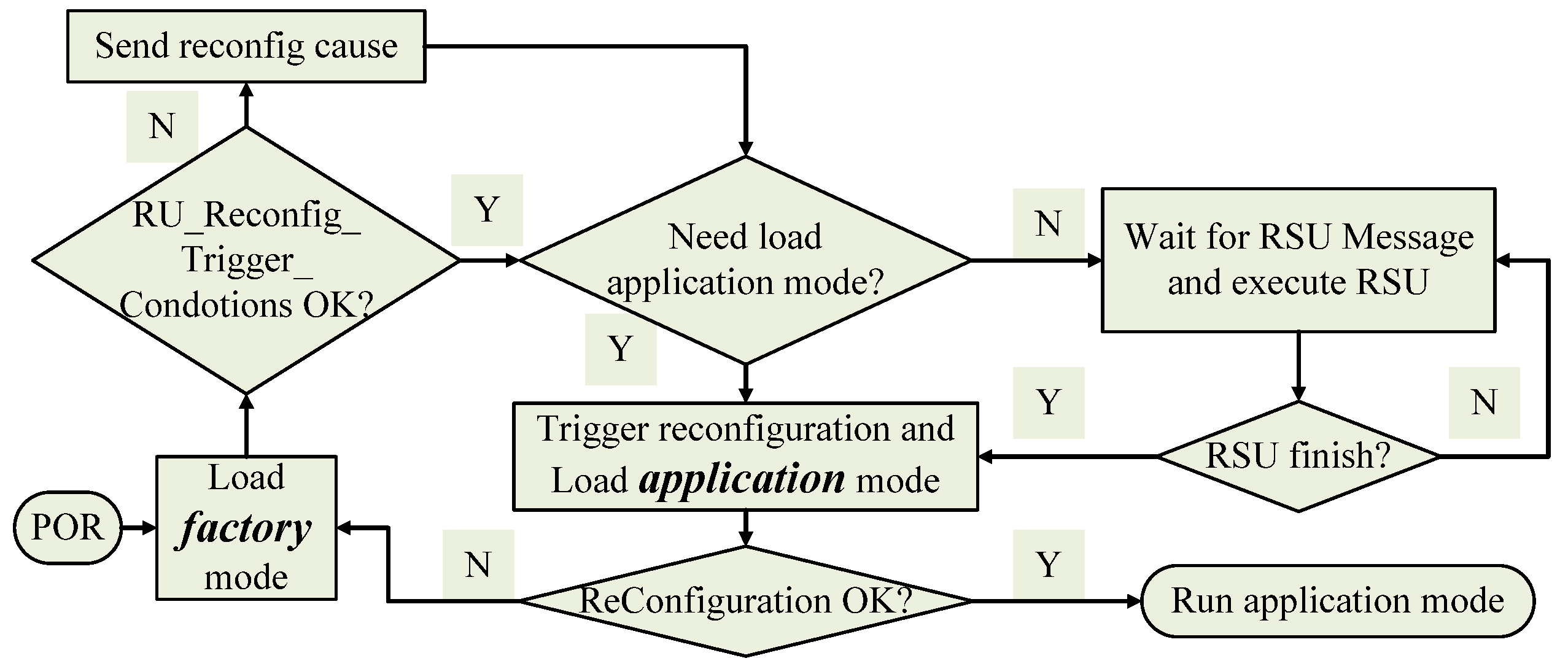
The process of switching and loading configuration images is demonstrated in Figure 3.
To begin with, SoPC automatically loads the factory mode after POR, and the RSU dedicated circuit sends the condition that triggers FPGA into a reconfiguration process if it exits. Then, SoPC reads parameters FnAy, Add_APP, and WD_TO from E2PROM. If FnAy is active, SoPC will begin to load the application mode image from the address of Add_APP, and set the watchdog timer time-out value as WD_TO, otherwise SoPC will stay in the factory mode to perform the RSU process. When SoPC enters RSU process, it should complete updating the application mode image and then trigger the reconfiguration to load it. If any error happens during the reconfiguration process, RSU dedicated circuit will force SoPC to load the factory mode image, and then record the condition that triggers the reconfiguration.
In this scheme, factory mode serves as a refresher and a safe. LC can always enter an exact and active state, and notice the UC when an error is detected. As a result, system reliability is improved. Because all nodes that need RSU are connected together by a single CAN bus, this scheme takes full advantage of the existing resources and suits distributed field control system.
2.2. Optimization of CAN Application Layer Protocol
RSU process makes use of the CAN 2.0B extended data frame, including 29-bit identifier (ID0 ~ID28) and eight-byte data field. In order to make full use of them, ID is classified into seven segments, as demonstrated in Table 1.
Digital ‘0’ of S0 refers to a frame from the UC, and digital ‘1’ of S0 means a message from a LC. Because digital ‘0’ presents a dominant bit and digital ‘0’ presents a recessive bit, and frames from UC is more important, UC has the higher transmit priority in accordance with the CAN arbitration scheme. If S1 is digital ‘0’, all the nodes should accept this frame, or only the specified nodes should do this. The number of UC is 0, and numbers of LCs increase progressively from 1. S5 indicates the message type, assigning 9 as RSU control messages and 10 as RSU data messages. The remaining IDs are reserved.
In the RSU data frames, the whole eight bytes of data field are pieces of the new SoPC configuration image. In terms of the RSU control frames, the higher four bytes of the data field represent the control type (RSU_CT), and the lower four bytes reveal the control message (RSU_CM). Moreover, RSU_CT and RSU_CM put to use so as to fulfill the shaking hands between UC and LC, configuration parameter transfer, data check, as well as the EPCS device burning command. In conclusion, the definition of RSU_CT between UC and LC is similar, as described in Table 2. While the definition of RSU_CM is different between UC and LC, as shown in Table 3.
In order to make full use of the CAN bus, the baud rate is set as 500 kilo bps and the bit timing set is in line with the CAN 2.0B standard strictly. In order to improve the communication efficiency, a hardware filter that is based on IDs is enabled. Thus, every LC only accepts messages from the UC, and UC accepts all messages. The hardware interruption of receiving is enabled, and the message handling program works in the interruption mode. As a result, RSU process does not occupy the core system resource all the time, and also, Nios II can take care of other affairs.
2.3. Flow of Transmitting a Configuration Image
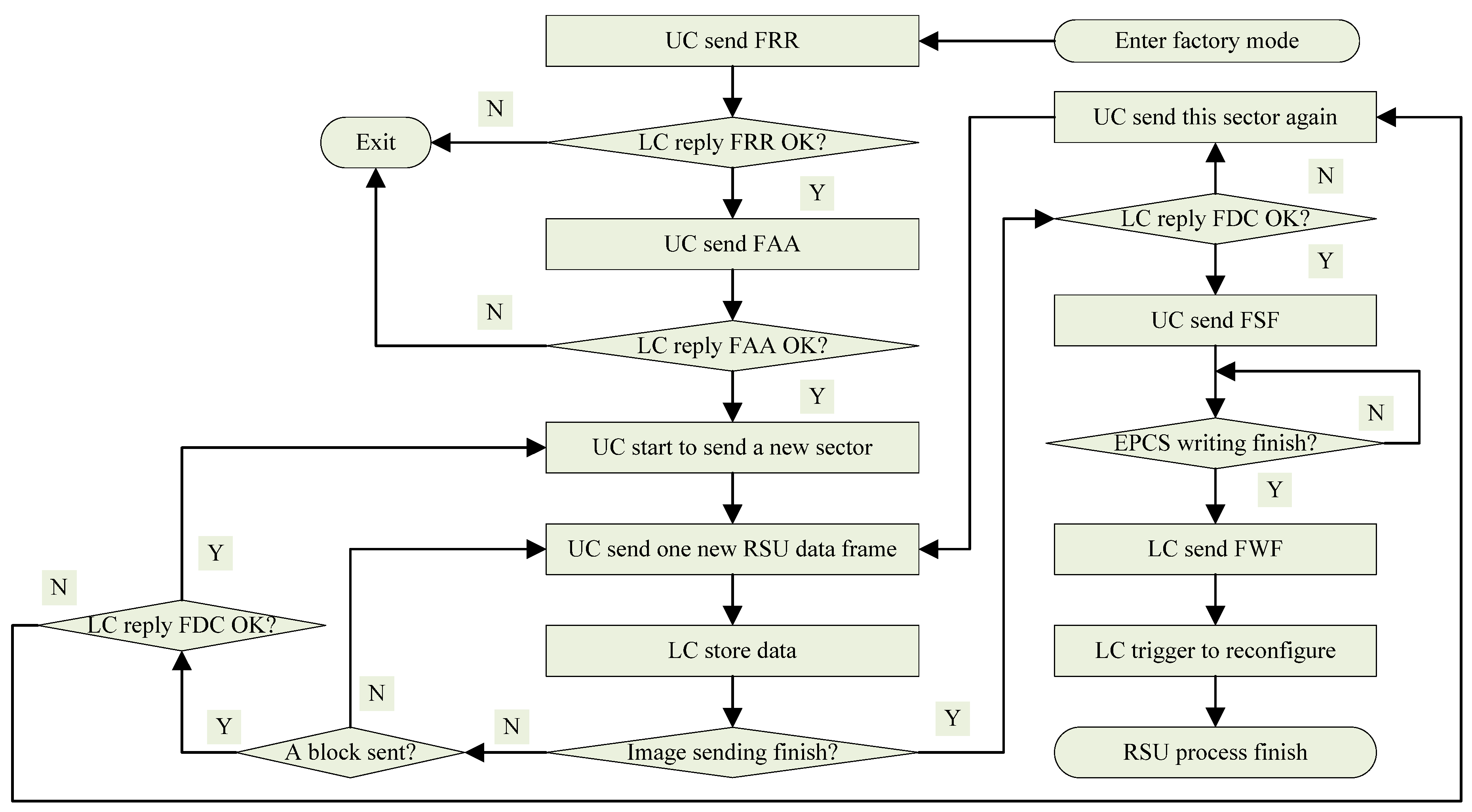
Software for both UC and LC is designed in the style of C/C++. The flow of the RSU process is demonstrated in Figure 4.
As mentioned above, SoPC enters the factory mode after POR, then UC and LC execute shaking hands by a FRR so as to ensure that the communication is OK. If the handshake check passes, UC stars to transfer the Add_APP by a FAA or quits the RSU process directly and warns the operator through the UC interface. In case LC receives a FAA successfully, it should store the parameter into E2PROM, and then read it back so as to check if data in E2PROM is the same as received. If it is, LC replies FAA OK and UC starts to send the new application configuration image. Otherwise, LC replies FAA failure and UC quits the RSU process so as to warn the operator.
In the configuration image transfer sub-process, UC loads 64 kB to its transmit buffer once, assuming the size of a block is 64 kB. If the remaining data is less than 64 kB, the hexadecimal digit F is used to fill the blanks in the last CAN frame’s data field, because the binary digit 1 is the initial state of EPCS device. Before transmission, UC has to check whether the integrated image has been transmitted by checking the internal pointer of the configuration image. If the transmission is not done, UC will employ the extended data frame to send the current data in buffer. Even if the CAN hardware employs the cyclic redundancy check to enhance its ability of detecting bit errors, it cannot avoid the arbitration error. Therefore, every frame that LC receives is dependable, but it is uncertain whether LC receives all frames or not. In order to handle this risk, whenever a block of data has been sent to LC, a data check will take place by FDC. As a tradeoff between reliability and efficiency, the sum check is applied. Every byte of data filed is regarded as an integer, and the sum of those eight integers is calculated. Furthermore, the total sum occupies four bytes.
Whenever UC sends a FDC, LC has to verify whether the results of data that checks from UC is the same as the results that calculates by itself. If the results match with each other, LC replies to UC that the data check is OK, then UC will continue to send the next block. Otherwise, LC replies to UC that the data check is failed, then UC will send this block again. When the total configuration image is sent, UC will send a FSF so as to inform LC, and execute the last data check. As discussed above, if LC replies to UC that the data check is failed, then UC will send those data again. Besides, if LC replies UC that the last data check is OK, LC will start to write all the data into the E2PROM. When E2PROM writing operation is done, LC will send a FWF so as to notice the operator. As a result, LC will trigger itself to reconfigure from the specified address by means of using the configuration image that is just received.
In terms of the flow, SoPC configuration image which is usually several MB is divided into some parts in the denomination of 64 kB. Even if there is any problem during the communication, it only costs sending a block again instead of sending the total configuration image. Therefore, the risk and cost of transmission error is reduced. Besides, it also indicates that the smaller block size can bring less risk and cost of the transmission error on the condition of enough capacity.
2.4. Design of the Advanced Boot Loader
When a SoPC configuration process begins, the RSU dedicated circuit provides the address where hardware part locates (Add_H), and also, the boot loader calculates the address where software part lies (Add_S) using the equation:
Add_S = 0x00 + Leng_H.
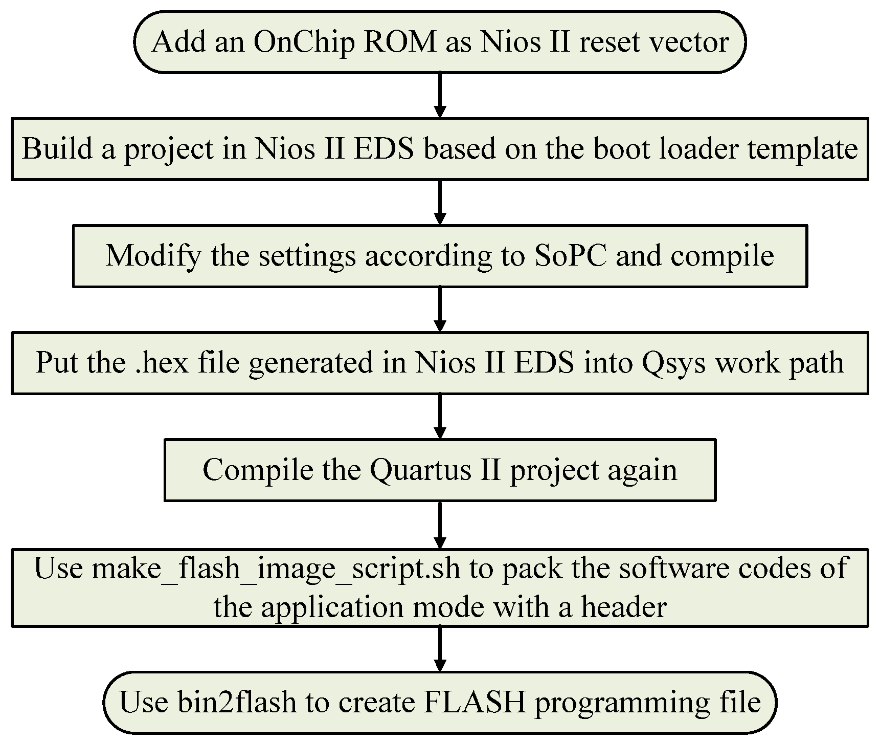
In Formula (1), Lenth_H is the length of hardware part, which is stored in the header of the hardware part. After POR, Add_H is initialized as 0x00 where the hardware part of the factory mode image locates exactly [25]. In a reconfiguration process, Add_H is in #4 register of RSU dedicated circuit interface (Table 4). As a result, the default boot loader works for the factory mode image, but unfortunately, it leads to the reference address error for the software part of the application mode image. Therefore, an advanced boot loader should be employed so as to specify where the software part of the application mode image locates. Besides, the flow of design and packaging of the advanced boot loader is demonstrated in Figure 5.
Qsys is a part of Quartus II design suit. Once the reset vector of Nios II is set to an on-chip memory, Quartus II will look for a hexadecimal-coded file (*.hex) with the same name as that of the on-chip memory. That hexadecimal-coded file contains programs for copying the software part of a configuration image. That is to say, the hexadecimal-coded file is the advanced boot loader.
To begin with, an on-chip memory that is no less than 16 kB should be added to the SoPC, and Nios II reset vector should be set to it in Qsys. Therefore, Quartus II will look for a hexadecimal-coded file (*.hex), which indicates where to carry the code of software part with the same name as the on-chip memory.
As a result, a new project working in Nios II EDS should be built by using the boot loader templates that are downloaded from the Altera company website. The address of software codes, the size of the EPCS device, as well as the size of the memory should be checked in the project. Besides, a hexadecimal-coded file and the advanced boot loader will arise in this project. After putting the hexadecimal-coded file into the working path of Qsys, the compilation in Quartus II results in the generation of the new FPGA device configuration file, with the advanced boot loader for the software part.
Because the advanced boot loader performs the version check by an additional header in the software part, a script named make_flash_image_script.sh is used to pack the software part with the combination of the version information into a binary-coded file (*.bin). Ultimately, a script named bin2flash is used to generate the FLASH programming file from that binary-coded file, so as to form the software part of the application mode image.
2.5. RSU Dedicated Circuit Operation Programs
In terms of the Quartus II 15.0 and later version, the Avalon-MM style interface for RSU dedicated circuit is available. It can realize the corresponding functions by means of modifying its internal registers. The registers of the RSU dedicated circuit interface for the Cyclone IV series devices are described in Table 4 [22].
Register #0 indicates which mode now the state machine is in. 0x00 means that now state machine is in the factory mode, and 0x01 refers to the application mode. Besides, register #0 can be read only. Register #1 is used to force the device to pull up the CONF_DONE signal a bit earlier before the total hardware configuration file is copied. Also, register #1 may be useful when there are multi-devices in a configuration network. Register #1 stores the overflow value of the watchdog timer, which can be disabled by writing the binary digit ‘0’ so as to register #3. Register #4 indicates where to load the application mode image. Moreover, writing the binary digit ‘0’ to register #5 enables the internal oscillator. Once the reconfiguration takes place, register #6 will record the reason that triggers FPGA. If one wants to reset the watchdog timer’s counter, write digit ‘1’ to register #7. Furthermore, writing the binary digit ‘1’ to register #8 will trigger SoPC to perform the reconfiguration immediately. Once the watchdog timer is active, it will check whether FPGA is still in control or not by monitoring the internal feedback signal.
According to Nios II EDS, writing and reading operations to the registers that have mentioned above can be achieved by the application programming interfaces (API). Specifically, the functions prototypes are IOWR (base, offset, data) and IORD (base, offset) [26].
2.6. EPCS Device Operation Programs
EPCS is a flash based device, and Nios II EDS provides API access to it. Function prototypes are alt_flash_open_dev() for purpose of opening the EPCS devices, alt_flash_close_dev() for closing the EPCS device, alt_erase_flash_block() for erasing the EPCS device, alt_write_flash() for writing the EPCS device, as well as alt_read_flash() for reading the EPCS device [26]. Flow of writing the EPCS device is demonstrated in Figure 6.
After the EPCS device is opened, the specific block should be erased so as to clear the residual data. In order to ensure that the data has been written correctly, data in the specific block will be read back after the finishing of the writing operation. Data read from the specific block matching data in the receive buffer means the writing operation is succeeded otherwise the writing operation to this block should be performed again. After the total content in the receive buffer has been written into EPCS device, EPCS device will be closed and the receive buffer will be clear.
3. Results
3.1. Experiment Environment and Equipment
The experiment applies a Terasic DE0-nano development board, a CAN transceiver board, as well as two USB-CAN hubs. The connection diagram and physical photo are shown in Figure 7.
The DE0-nano development board has an Altera EP4CE22F16 device, and an EPCS 64 device whose block size is 64 kB [27]. The RSU control platform is used to generate the application mode image, and control the transmission process through USB-CAN #1. Besides, the CAN monitor platform is used to monitor the work state of CAN bus and record every frame that appears on the bus via USB-CAN #2.
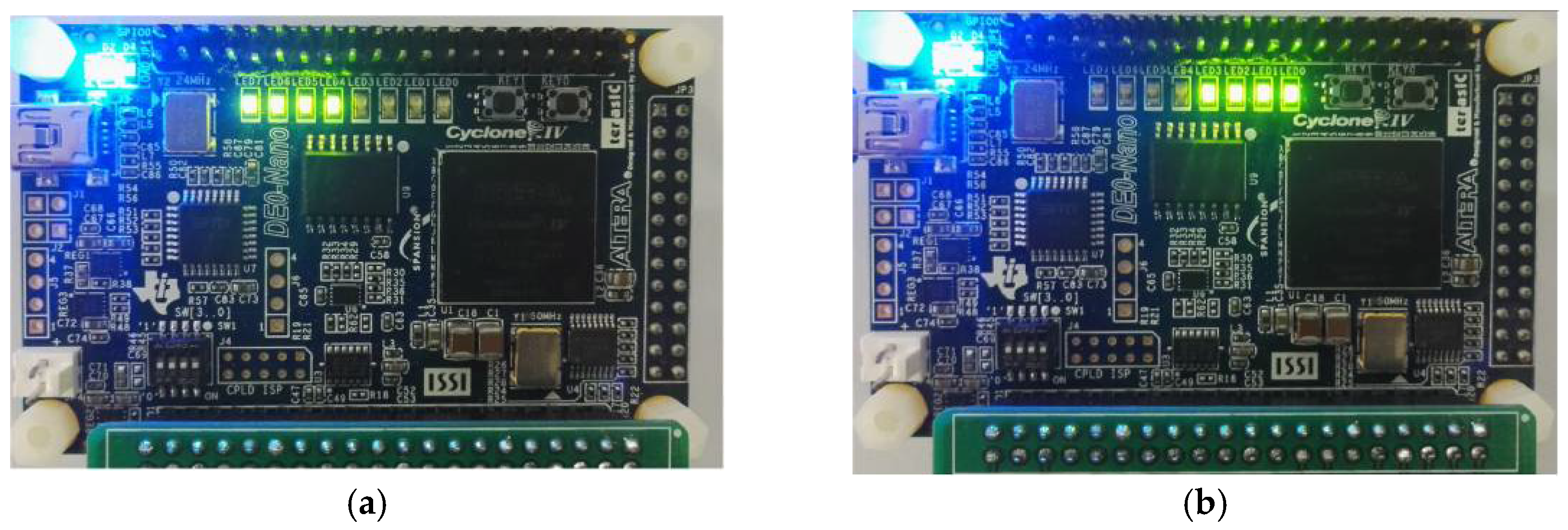
Eight light emitting diodes (LEDs) on DE0-nano board are used to distinguish among the factory mode image and the application mode image. With respect to the factory mode image, the higher four LEDs will light, but the lower four LEDs will light in the application mode image.
3.2. Measurement of Key Signals and LED Lighting During Reconfigurations
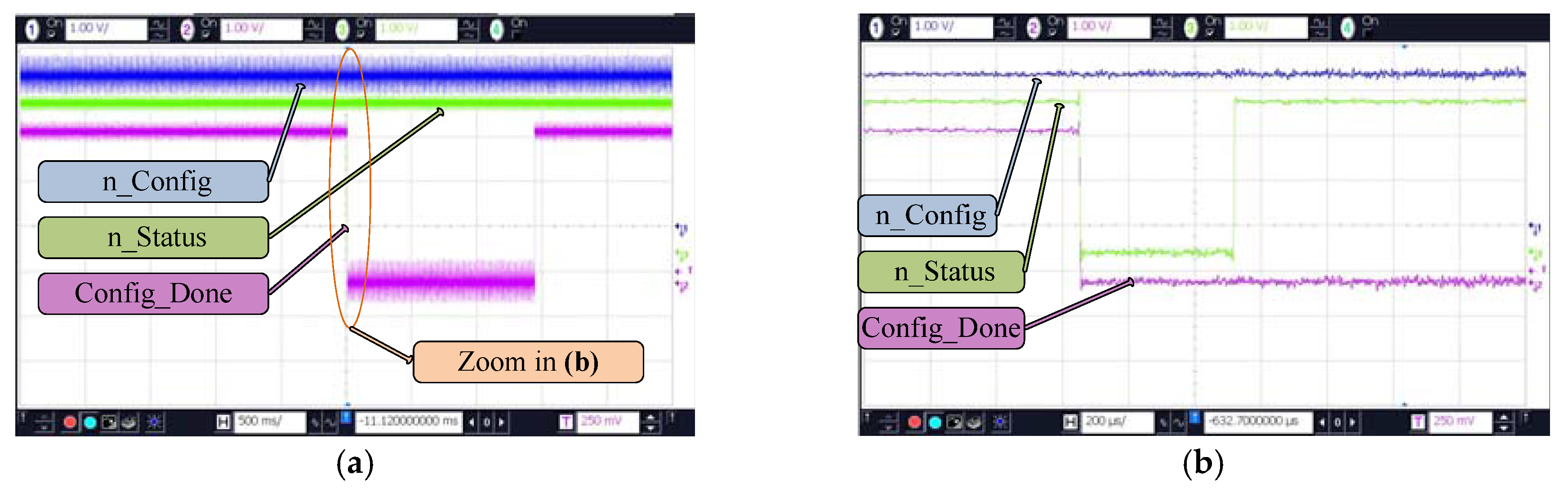
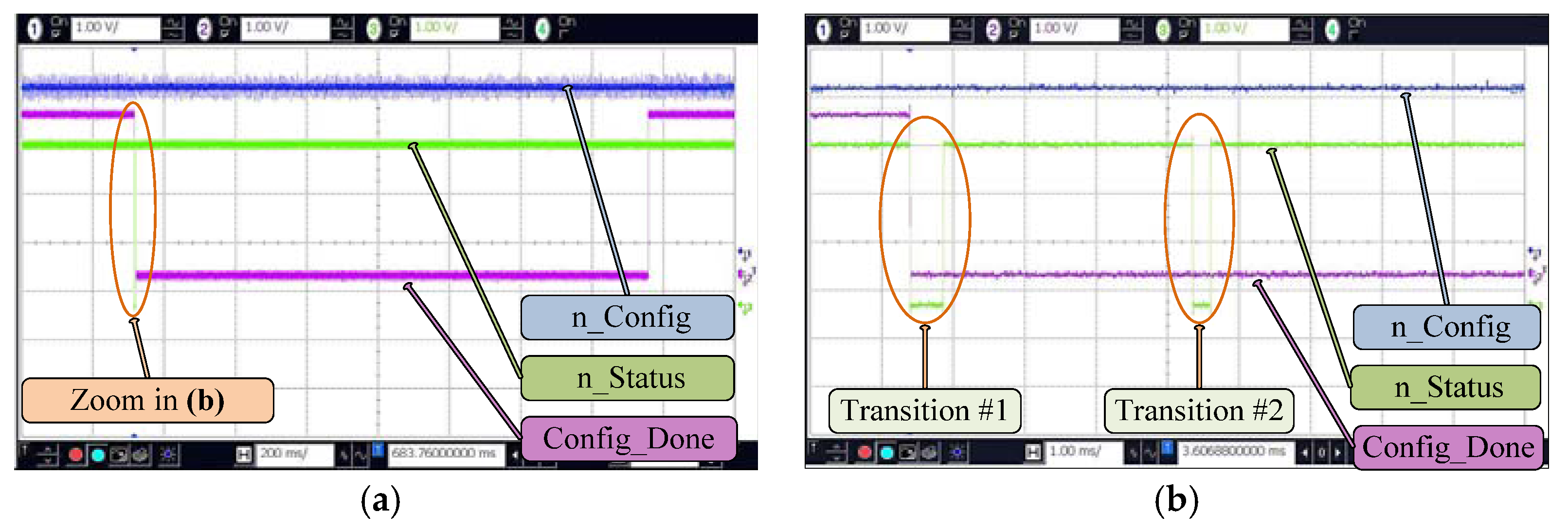
During Altera FPGA’s configuration process, n_Status, n_Config, and Config_Done are key signals. When FPGA chip powers up, it asserts these signals low. The n_Config signal will keep low until POR is done. After that, n_Status signal will stay low until the FPGA internal reset process is finished. When the configuration process succeeds, the Config_Done signal will go high. A reconfiguration is realized by means of pulling the n_Status signal low using the RSU dedicated circuit. The waveform of the key signals during a reconfiguration process is demonstrated in Figure 8.
It can be seen that when FPGA begins to reconfigure, the n_Status signal goes low as well as the Config_Done signal. When the FPGA enters a new configuration process, the n_Status signal goes high. At the same time, when the FPGA finishes a new configuration, the Config_Done signal also goes high. Those phenomena reveal the success of a reconfiguration. The experiment phenomena on the DE0-nano board before and after RSU are shown in Figure 9.
It is obvious that the higher four LEDs are lit before RSU, but the lower four LEDs are lit after RSU. It demonstrates that the factory mode image works fine, and the application mode image is loaded successfully after a reconfiguration process. Therefore, the RSU process works.
4. Discussion
4.1. Time Consumed in RSU Process
As mentioned above, the RSU request produces two frames, as well as sending the address of the application mode software codes. Assuming that there is no problem in the process of transmitting a new image, sending an entire block will take 8192 frames for the data of image, and another two frames for the data check. If the last block is not full with the valid data, the number of frames for transmitting the data of image will be the bytes of the valid data that is divided by 8. Furthermore, two frames for the data check is still necessary. In the end, two frames are required for E2PROM writing. Therefore, the total number of frames is 43,828, which is the same as the counting result of the CAN monitor platform. Therefore, the transmitting process is correct.
Sending a CAN frame will consume 0.01 s. Because this kind of CAN frames have the overall majority, the total time consumed can be calculated as approximately
0.01 s × 43828 ≈ 438 s.
As a result, the total time of transmitting the configuration image is less than 8 min, which saves a lot of time and manpower, making the system easy to repair and promote.
In fact, the minimum time of sending an extended data frame is about 307 us at the baud rate of 500 kbps. Nevertheless, the UC works on the Windows operation system, which is not a real time, making the software execution time remain unstable. Besides, once the arbitration error takes place, UC has to send the frame again, which will bring the tricky troubles when designing the software in a periodic mode. As a result, time margin for sending a frame is reserved. Thus, the VxWorks real time operation system is a better choice in the forward work [28].
A baud rate of 500 kbps is relatively high, and it could lead to an overload problem for UC since the receiving of all frames for UC. In order to handle the underlying problem, a memory that is based on the direct memory access (DMA) scheme will be considered in the future work [29].
4.2. Verification of Factory Mode as a Safe
The application mode image is erased so as to check whether FPGA can roll back to the factory mode image or not if it attempts to execute a reconfiguration from the address of Add_APP. A FWF is sent by the CAN monitor, and the waveform of those key signals in this process is shown in Figure 10.
In accordance with the Figure 10, FPGA tries to reconfigure twice due to two transitions on the n_Status signal. The first rising edge of the n_Status signal is caused by the trial of the reconfiguration from the address of Add_APP. After the failure of the first trial, FPGA is forced to load the factory mode image, which results in the second rising edge of n_Status signal. Ultimately, the Config_Done signal is released high, indicating the factory mode is loaded successfully. Therefore, the factory mode image acts as safe when the application mode image is damaged.
However, the industrial applications are expected to have better reliability. Transient voltage suppression diodes that are paralleled with EPCS device pins should be added so as to avoid damage from unknown surges. Furthermore, the factory mode image could locate at the place of an external parallel FLASH device in the active parallel (AP) programming mode [25]. By means of disabling the writing operation to the blocks where the factory mode image locates, risk of modification to the factory mode image can be eliminated. Efforts will be paid on those topics in the future work so as to protect the factory mode image physically.
5. Conclusions
A SoPC RSU scheme employing RSU dedicated circuit and CAN bus is proposed and verified in this article. The RSU dedicated circuit chooses to load the factory mode image or application mode image stored in the EPCS device. The factory mode configuration image acts as a safeguard, ensuring system can roll back to a known state when RSU process fails. SoPC uses the CAN bus interface to receive new configuration images directly, making the proposed scheme suitable for distributed control systems. Optimized CAN application layer protocol and new configuration image transmitting sub process reduce risk and cost of transmission error and makes full use of CAN 2.0B frames. The advanced boot loader can specifically address where in the software a part locates to help the application mode work. This experiment demonstrates the feasibility of this scheme, including reconfiguration from the new application mode image and rolling back to the factory mode image when there’s no effective application mode image. However, long time tests and harsh environment tests should be practiced to confirm and improve the reliability of this scheme in the future.
Acknowledgments
This work was supported by Fundamental Research Funds for the Central Universities under Grant No. 2682014CX086.
Author Contributions
This research was accomplished by all authors listed. Lei Zhou, Bangji Wang, and Qingxiang Liu raised this theme, investigated the state of this research field and proposed the primary principle and main methods. Peixin Yang participated in software debugging and preparation for all experiments. Xiangqiang Li and Jianqiong Zhang contributed to data recording and analysis, as well as manuscript preparation.
Conflicts of Interest
The authors declare no conflict of interest.
References
- Tayara, H.; Ham, W.; Chong, K.T. A Real-Time Marker-Based Visual Sensor Based on A FPGA and A Soft Core Processor. Sensors 2016, 16, 2139. [Google Scholar] [CrossRef] [PubMed]
- Chen, J.H.; Yau, H.T.; Lu, J.H. Implementation of FPGA-Based Charge Control for a Self-Sufficient Solar Tracking Power Supply System. Appl. Sci. 2016, 6, 41. [Google Scholar] [CrossRef]
- Liu, H.J.; Li, K.J.; Lee, W.J.; Gao, H. Development of Frequency Variable Inverter Based on SOPC and Nios II. IEEE Trans. Ind. Appl. 2013, 49, 2237–2243. [Google Scholar] [CrossRef]
- Szadkowski, Z.; Fraenkel, E.D.; van den Berg, V.D. FPGA/NIOS Implementation of an Adaptive FIR Filter Using Linear Prediction to Reduce Narrow-Band RFI for Radio Detection of Cosmic Rays. IEEE Trans. Nucl. Sci. 2013, 60, 3483–3490. [Google Scholar] [CrossRef]
- Hoffmeyer, J.; Park, I.P.; Majmundar, M.; Blust, S. Radio Software Download for Commercial Wireless Reconfigurable Devices. IEEE Commun. Mag. 2004, 42, S26–S32. [Google Scholar] [CrossRef]
- Nilchiani, R. Valuing Software-based Options for Space Systems Flexibility. Acta Astronaut. 2009, 65, 429–441. [Google Scholar] [CrossRef]
- Chang, Y.C.; Chi, T.Y.; Wang, W.C.; Kuo, S.Y. Dynamic Software Update Model for Remote Entity Management of Machine-to-machine Service Capability. IET Commun. 2013, 7, 32–39. [Google Scholar] [CrossRef]
- Sünter, I.; Slavinskis, A.; Kvell, U.; Vahter, A. Feature article: Firmware Updating Systems for Nanosatellites. IEEE Aerosp. Electron. Syst. Mag. 2016, 31, 36–44. [Google Scholar] [CrossRef]
- Ji, W.J.; Li, X.Q.; Chen, J.Y. Remote Update on Flash-Based Hydrologic Remote Terminal through GPRS Technology. Adv. Mater. Res. 2013, 846–847, 1711–1715. [Google Scholar] [CrossRef]
- Zhang, J.; Liao, Z.; Zhu, L. Research on Design and Implementation of Automotive ECUs Software Remote Update. Adv. Mater. Res. 2015, 740, 847–851. [Google Scholar] [CrossRef]
- Guo, C.J.; Miao, C.Y.; Wu, Z.G.; Xi, L.N. Research and Implementing of Remote Update for Network Telephone System Program Based on Ethernet. In Proceedings of the 2010 2nd International Conference on Signal Processing Systems (ICSPS), Dalian, China, 5–7 July 2010; pp. 280–283. [Google Scholar]
- Qi, S.B.; Zhang, M.; Wang, Z.H. Remote Multi-processor Updating System Based on In-system Programming and CAN-bus. Appl. Mech. Mater. 2013, 364, 419–423. [Google Scholar] [CrossRef]
- Zhang, X.; Tang, L.B.; Ji, M.P. Remote Updating for DSP and FPGA Programs. In Proceedings of the 2015 IET International Radar Conference (IRC), Hangzhou, China, 14–16 October 2015; pp. 1–4. [Google Scholar]
- Makowski, D.; Jabłoński, G.; Perek, P.; Mielczarek, A.; Prędki, P.; Schlarb, H.; Napieralski, A. Firmware Upgrade in xTCA Systems. IEEE Trans. Nucl. Sci. 2013, 60, 3639–3646. [Google Scholar] [CrossRef]
- Fernandes, A.; Pereira, R.C.; Sousa, J.; Carvalho, P.F.; Correia, M.; Rodrigues, A.P.; Carvalho, B.B.; Correia, C.M.B.A.; Gonçalves, B. FPGA Remote Update for Nuclear Environments. IEEE Trans. Nucl. Sci. 2016, 3, 1645–1649. [Google Scholar] [CrossRef]
- Vliegen, J.; Mentens, N.; Verbauwhede, I. Secure, Remote, Dynamic Reconfiguration of FPGAs. ACM Trans. Reconfigurable Tech. Syst. 2015, 7, 1–19. [Google Scholar] [CrossRef]
- Guzmán, D.; Prieto, M.; García, D.; Ruíz, V.; Almena, J.; Sánchez, S.; Meziat, D. High Reliable Remote Terminal Unit for Space Applications. In Proceedings of the 2009 12th Euromicro Conference on Digital System Design, Architectures, Methods and Tools (ECDSDAMT), Patras, Greece, 27–29 August 2009; pp. 488–493. [Google Scholar]
- Meng, H.; Pan, L. Design of Update for Remote Device Based on GPRS. Adv. Mater. Res. 2014, 926–930, 1910–1913. [Google Scholar] [CrossRef]
- Badrignans, B.; Champagne, D.; Elbaz, R.; Gebotys, C.; Torres, L. SARFUM: Security Architecture for Remote FPGA Update and Monitoring. ACM Trans. Reconfigurable Techol. Syst. 2010, 3, 8–36. [Google Scholar] [CrossRef]
- Basile, B.; Carlo, S.D.; Scionti, A. FPGA-based Remote-code Integrity Verification of Programs in Distributed Embedded Systems. IEEE Trans. Syst. Man Cybern. C 2012, 42, 187–200. [Google Scholar] [CrossRef]
- Bing, B. A Fast and Secure Framework for Over-the-air Wireless Software Download Using Reconfigurable Mobile Devices. IEEE Commun. Mag. 2006, 4, 58–63. [Google Scholar] [CrossRef]
- Altera Remote Update IP Core User Guide. Available online: https://www.altera.com.cn/content/dam/altera-www/global/en_US/pdfs/literature/ug/ug_altremote.pdf (accessed on 10 April 2017).
- Alternative Nios II Boot Methods. Available online: https://www.altera.com.cn/content/dam/altera-www/global/en_US/pdfs/literature/an/an458.pdf (accessed on 19 August 2016).
- Sanchez, A.; Prieto, M.; Polo, O.R.; Parra, P.; Sliva, A.D.; Gutierrez, O.; Castillo, R.; Fernandez, J.; Pacheco, J.R. HW/SW Co-design of the Instrument Control Unit for the Energetic Particle Detector on-board Solar Orbiter. Adv. Space Res. 2013, 6, 989–1007. [Google Scholar] [CrossRef]
- Cyclone IV Device Handbook. Available online: https://www.altera.com/content/dam/altera-www/global/en_US/pdfs/literature/hb/cyclone-iv/cyclone4-handbook.pdf (accessed on 1 December 2016).
- Nios II Classic Software Developer’s Handbook. Available online: https://www.altera.com.cn/content/dam/altera-www/global/en_US/pdfs/literature/hb/nios2/n2sw_nii5v2.pdf (accessed on 14 May 2015).
- Serial Configuration (EPCS) Devices Datasheet. Available online: https://www.altera.com.cn/content/dam/altera-www/global/zh_CN/pdfs/literature/hb/cfg/cyc_c51014.pdf (accessed on 21 June 2016).
- Yu, Y.; Liu, Q.X.; Zhao, L.; Wang, B.J.; Zhang, Z.Q.; Li, X.Q.; Zhang, J.Q. Design of the Master Control System of the Array Antenna Based on the VxWorks. In Proceedings of the 2011 International Conference on Intelligent Computation Technology and Automation (ICICTA), Shenzhen, China, 22–29 March 2011; pp. 516–518. [Google Scholar]
- ECAN Operation with DMA on dsPIC33F and PIC24H Devices. Available online: http://ww1.microchip.com/downloads/en/appnotes/01249a.pdf (accessed on 16 January 2009).
Figure 1.
Brief of the remote system update.

Figure 2.
Composition of the proposed RSU scheme.

Figure 3.
Process of switching and loading the configuration images.

Figure 4.
Flow of transmitting a configuration image.

Figure 5.
Design flow of the advanced boot loader.

Figure 6.
Flow of writing the EPCS device.

Figure 7.
Experiment environment: (a) for connection diagram; (b) for physical photo.

Figure 8.
Transition of key signals during a reconfiguration: (a) preview in a large time scale; (b) zoom in on the transition edges in a short time scale.
Figure 8.
Transition of key signals during a reconfiguration: (a) preview in a large time scale; (b) zoom in on the transition edges in a short time scale.

Figure 9.
LEDs lighting states: (a) before reconfiguration; (b) after reconfiguration.

Figure 10.
Transitions of key signals in the process: (a) preview in a large time scale; (b) zoom in on the transition edges in a short time scale.
Figure 10.
Transitions of key signals in the process: (a) preview in a large time scale; (b) zoom in on the transition edges in a short time scale.


Table 1.
Segments of IDs in the application layer protocol
| Segment NO. | Associated IDs | Explanation |
|---|---|---|
| S0 | D28 | Message direction |
| S1 | D27 | Transmission type |
| S2 | D26~D23 | Reserved |
| S3 | D22~D16 | CAN node number |
| S4 | D15~D10 | Reserved |
| S5 | D9~D5 | Message type |
| S6 | D4~D0 | Reserved |
Table 2.
Definition of RSU_CT
| RSU_CT for UC | RSU_CT for LC | RSU Command Type Explanation |
|---|---|---|
| 0x01 | 0x11 | Frame of RSU request (FRR) |
| 0x02 | 0x12 | Frame of APP mode image address (FAA) |
| 0x03 | 0x13 | Frame of data check (FDC) |
| 0x04 | 0x14 | Frame of image sending finished (FSF) |
| 0x05 | 0x15 | Frame of EPCS writing finished (FWF) |
Table 3.
Definition of RSU_CM
| Command Type | Definition for UC | Definition for LC |
|---|---|---|
| FRR | Fixed with 0x01 | Fixed with 0x01 |
| FAA | Fixed with 0x02 | Fixed with 0x02 |
| FDC | Data check result | 0x00 for data check is OK or failure |
| FSF | Data check result | 0x00 for data check is OK or failure |
| FWF | Fixed with 0x01 | Fixed with 0xFFFFFFFF |
Table 4.
Registers of the RSU dedicated circuit
| Address Offset | Register Name | Register Number |
|---|---|---|
| 0x00 | RU_MASTER_SM_CURRENT_STATE_MODE | 0 |
| 0x04 | RU_FORCE_EARLY_CONF_DONE | 1 |
| 0x08 | RU_WATCHDOG_TIMEOUT | 2 |
| 0x0C | RU_WATCHDOG_ENABLE | 3 |
| 0x10 | RU_BOOT_ADDRESS | 4 |
| 0x14 | RU_FORCE_INTERNAL_OSC | 5 |
| 0x18 | RU_RECONFIG_TRIGGER_CONDITION | 6 |
| 0x1C | RU_RESET_TIMER | 7 |
| 0x1D | RU_RECONFIG | 8 |
© 2017 by the authors. Licensee MDPI, Basel, Switzerland. This article is an open access article distributed under the terms and conditions of the Creative Commons Attribution (CC BY) license (http://creativecommons.org/licenses/by/4.0/).
Share and Cite
MDPI and ACS Style
Zhou, L.; Liu, Q.; Wang, B.; Yang, P.; Li, X.; Zhang, J. Remote System Update for System on Programmable Chip Based on Controller Area Network. Electronics 2017, 6, 45. https://0-doi-org.brum.beds.ac.uk/10.3390/electronics6020045
AMA Style
Zhou L, Liu Q, Wang B, Yang P, Li X, Zhang J. Remote System Update for System on Programmable Chip Based on Controller Area Network. Electronics. 2017; 6(2):45. https://0-doi-org.brum.beds.ac.uk/10.3390/electronics6020045
Chicago/Turabian StyleZhou, Lei, Qingxiang Liu, Bangji Wang, Peixin Yang, Xiangqiang Li, and Jianqiong Zhang. 2017. "Remote System Update for System on Programmable Chip Based on Controller Area Network" Electronics 6, no. 2: 45. https://0-doi-org.brum.beds.ac.uk/10.3390/electronics6020045
Note that from the first issue of 2016, this journal uses article numbers instead of page numbers. See further details here.