Hardware Optimized and Error Reduced Approximate Adder


School of Computer Science and Engineering, Nanyang Technological University, 50 Nanyang Avenue, Singapore 639798, Singapore
*
Author to whom correspondence should be addressed.
Electronics 2019, 8(11), 1212; https://0-doi-org.brum.beds.ac.uk/10.3390/electronics8111212
Submission received: 22 September 2019
/
Revised: 15 October 2019
/
Accepted: 22 October 2019
/
Published: 24 October 2019
(This article belongs to the Section Circuit and Signal Processing)
Abstract
:This paper presents a new hardware optimized and error reduced approximate adder (HOERAA), which is suitable for field programmable gate array (FPGA)- and application specific integrated circuit (ASIC)-based implementations. In this work, we consider a FPGA-based implementation using Xilinx Vivado 2018.3, targeting an Artix-7 FPGA. The ASIC-based realizations are based on a 32/28nm complementary metal oxide semiconductor (CMOS) process. Based on FPGA implementations, we note the following: (i) For 32-bit addition involving a 8-bit least significant inaccurate sub-adder, HOERAA requires 22% fewer look-up tables (LUTs) and 18.6% fewer registers while reducing the minimum clock period by 7.1% and reducing the power-delay product (PDP) by 14.7%, compared to the native accurate FPGA adder, and (ii) for 64-bit addition involving a 8-bit least significant inaccurate sub-adder, HOERAA requires 11% fewer LUTs and 9.3% fewer registers while reducing the minimum clock period by 8.3% and reducing the PDP by 9.3%, compared to the native accurate FPGA adder. Based on ASIC-style implementations, HOERAA is found to achieve the following reductions in design metrics compared to an optimum accurate carry-lookahead adder: (i) A 15.7% reduction in critical path delay, a 21.4% reduction in area, and a 35% reduction in PDP for 32-bit addition involving a 8-bit least significant inaccurate sub-adder, and (ii) a 15.3% reduction in critical path delay, a 10.7% reduction in area, and a 20% reduction in PDP for 64-bit addition involving a 8-bit least significant inaccurate sub-adder. Moreover, comparisons with other approximate adders show that HOERAA has a significantly reduced average error, mean average error, and root mean square error, while reporting near optimum design metrics.
1. Introduction
Approximate computing is emerging as a viable low power alternative to conventional accurate computing [1], especially for practical digital signal processing applications which underlie modern electronics, computer, and communication engineering. Whether it be big data analytics [2], software engineering [3], neuromorphic computing [4], hardware realization of deep neural networks for machine learning and artificial intelligence [5], memory systems for multicore processors [6,7], low power graphics processing units [8], and ultra-low power electronic design involving sub-threshold operation of devices [9], approximate computing is being resorted to in the quest for achieving greater efficiency in computing [10]. Approximate computing takes advantage of the inherent error resilience of practical multimedia applications [11].
Approximate computing spans both hardware and software, and in this work, the focus is on the design of approximate hardware. With respect to approximate hardware, the research focus has been predominant on approximate logic circuits [12] and approximate arithmetic circuits such as adders and multipliers [13]. Here, the focus is on the design of an approximate adder.
Many approximate adders in the existing literature are suited for an application specific integrated circuit (ASIC)-style implementation and only some are suitable for both ASIC- and field programmable gate array (FPGA)-based implementations. Hence, it is unlikely that many approximate adders in the literature, when implemented on an FPGA, would surpass a native accurate FPGA adder of similar size because an FPGA embeds accurate arithmetic units, such as adders and multipliers, which are highly optimized for speed and area.
This paper proposes a new approximate adder that is suitable for FPGA- and ASIC-based implementations, and our focus is on a comparison with other approximate adders, which are also suited for FPGA- and ASIC-based implementations. The remainder of this paper is organized as follows. A survey of some popular existing literature on approximate adders is presented in Section 2. Following this, we present the proposed approximate adder (HOERAA) in Section 3. FPGA-based implementation results corresponding to accurate and approximate adders for 32-bit and 64-bit additions are given in Section 4. ASIC-based implementation results of the accurate and approximate adders are also provided in Section 4. Further, the error characteristics corresponding to the various approximate adders, including the proposed HOERAA, are discussed in Section 4. Finally, we conclude in Section 5.
2. Literature Survey
In this section, we survey some popular literature on approximate adders.
Zhu et al. [14] proposed the first approximate adder that consists of two sub-adders, out of which one is accurate and the other is inaccurate. Several approximate adders presented subsequently in the literature followed this approach of bi-partitioning an approximate adder into accurate and inaccurate sub-adders. The inaccurate sub-adder is less significant while the accurate sub-adder is more significant. Addition can be performed simultaneously in the accurate and inaccurate sub-adders because the carry input of the accurate sub-adder is set to 0 [14]. A custom control logic is provisioned for the inaccurate sub-adder and an ASIC-based implementation was done.
Zhu et al. subsequently proposed improved variants of their approximate adder in References [15,16]. However, these approximate adders are ASIC-oriented, like in Reference [14], and may not be suitable for a FPGA-based implementation. For an example, we considered the Type II error tolerant adder of Reference [15], called ETAII, for a FPGA implementation. We used Vivado 2018.3 and targeted an Artix-7 FPGA (part: xc7a100tcsg324-3) by adopting the synthesis strategy as Flow_AreaOptimized_high. The default implementation strategy was used. The 32-bit ETAII reports a maximum frequency of 454.545 MHz (i.e., a clock period of 2.2 ns) and requires 53 look-up tables (LUTs) and 97 flip-flops (registers) for implementation. In contrast, the 32-bit (native) accurate FPGA adder has a maximum frequency of 476.19 MHz (clock period of 2.1 ns) and requires only 32 LUTs and the same number of flip-flops as ETAII. Thus, the accurate FPGA adder reports a 4.8% increase in the maximum frequency over the approximate adder ETAII and requires 40% less LUTs. The big increase in the number of LUTs for ETAII compared to the accurate FPGA adder is due to the introduction of a custom control logic to facilitate the approximation. This implies that all the ASIC-oriented approximate adders may not be suitable for realization in an FPGA-based design environment as it may become counterproductive.
Yang et al. [17] and Gupta et al. [18] presented transistor-level approximate full adders which can be used to construct approximate adders. These approximate adders also comprise an accurate sub-adder and an inaccurate sub-adder, similar to Reference [14]. References [17] and [18] correspond to ASIC-based implementations. Nevertheless, the approximate adder utilizing the type 5 approximate full adder of Reference [18], is suitable for a FPGA-based implementation. This is because the type 5 approximate full adder of Reference [18] uses the equation SUMi = Bi for the sum output (SUM), where B is an adder input and i denotes a bit position. There are no carry outputs or carry propagation from one full adder to another in the inaccurate sub-adder and only the sum outputs are produced. Hence, the type 5 approximate full adder of Reference [18] will not require a LUT for a FPGA-based implementation but requires a non-inverting buffer for an ASIC-based implementation. The carry input to the accurate sub-adder is simply the adder input Ai–1.
Mahdiani et al. [19] and Albicocco et al. [20] presented approximate adders which are suitable for both ASIC- and FPGA-based implementations. These approximate adders also incorporate an accurate sub-adder and an inaccurate sub-adder. The topological difference between Reference [19] and Reference [20] is that the AND of the most significant input bit-pair of the inaccurate sub-adder is provided as the carry input for the accurate sub-adder in Reference [19], whereas the carry input of the accurate sub-adder is set to 0 in Reference [20]. In References [19] and [20], all the input bit pairs of the inaccurate sub-adder are OR-ed to produce the corresponding sum bits.
Recently, Dalloo et al. [21] presented a slightly modified version of the approximate adder of [19]. However, the accurate sub-adders of References [21] and [19] are the same. Nevertheless, in Reference [21], the two most significant bit-pairs of the inaccurate sub-adder are alone logically OR-ed to produce the corresponding sum bits as Reference [19], while the rest of the less significant sum bits of the inaccurate sub-adder are set to Vdd (i.e., binary 1).
Echavarria et al. [22] proposed possibly the first FPGA-only approximate adder, called FAU, which also comprises an accurate sub-adder and an inaccurate sub-adder. In the inaccurate sub-adder, the inputs between adjacent LUTs are shared to minimize the error in the corresponding sum bits, while the accurate sub-adder could make use of the fast carry logic embedded in an FPGA slice. However, the drawback with Reference [22] is that only ASIC-oriented approximate adders, such as References [15,23,24,25,26], were considered for a FPGA implementation and comparison, and the native accurate FPGA adder was left out of the comparison, as pointed out in Reference [27]. Based on a Virtex-7 FPGA implementation using Vivado 2015.1, it was noted in Reference [27] that the 32-bit and 64-bit FAU of [22] report maximum frequencies of 328.19MHz and 281.06MHz respectively, whereas the native accurate 32-bit and 64-bit FPGA adders report significant increases in maximum frequencies by 116% and 85%. Given this, FAU is unlikely to be considered for a FPGA-based implementation of approximate computer arithmetic.
The approximate adder proposed in Reference [27] also contains an accurate sub-adder and an inaccurate sub-adder, and it is suitable for FPGA- and ASIC-based implementations. It has been observed in Reference [27] that this approximate adder has a reduced error range and has better error characteristics than the approximate adders of References [19] and [20], while reporting nearly similar design metrics.
The approximate adders discussed thus far feature a static approximation where the size of the accurate and the inaccurate sub-adders are pre-fixed, and this can be done commensurate with an application. There is, however, another category of approximate adders which incorporate a dynamic approximation where the level of approximation may be varied on demand. Additionally, the production of approximate or accurate outputs is possible based on need. References [23,24,25,26] discuss dynamic approximate adders which incorporate extra carry prediction and control units or error detection and correction circuits to be able to produce approximate or accurate outputs as required. In conjunction with the approximate adder logic, these extra circuitries would consume more resources (LUTs) when implemented on a FPGA and, consequently, they would lead to inferior design metrics compared to the native accurate FPGA adder. This issue had been discussed in Reference [22]. Moreover, it has been observed in Reference [28] that the power dissipation of the dynamic approximation hardware is comparable to that of the static approximation hardware due to the following: (i) The area overhead resulting from the introduction of extra circuitries for error detection and/or correction in [23,24,25,26], and (ii) the use of multiple clock cycles to produce the accurate output or an approximate output subject to the desired level of accuracy.
3. Accurate and Approximate Adders
The architecture of an N-bit accurate adder and the generic architectures of N-bit approximate adders are shown in Figure 1. For the approximate adders, we define the size of the least significant inaccurate sub-adder to be K-bits, and hence the size of the more significant accurate sub-adder will be (N–K)-bits. A and B represent the adder inputs in Figure 1, while SUM denotes the sum output, which includes a carry overflow bit. The subscripts associated with the adder inputs and outputs denote the corresponding bit positions. The (N–K) sum bits of the accurate sub-adder are combined with the K sum bits of the inaccurate sub-adder to produce the N sum bits of approximate adders, which includes the carry overflow.
We shall use some legends for the approximate adders for the ease of referencing; some of the legends are defined by the authors in their respective works while the remaining are defined by us in this work for referencing.
The accurate adder is shown in Figure 1a. The approximate adder of Reference [19], called the lower-part OR adder (LOA), is shown in Figure 1b. In the LOA, the K input bit-pairs of the inaccurate sub-adder are respectively OR-ed to produce the K sum bits. The most significant bit-pair of the inaccurate sub-adder viz. AK–1 and BK–1 is alone AND-ed and given as the carry input for the accurate sub-adder.
The approximate adder of Reference [20] shall be referred to as LOAWA (i.e., LOA without the 2-input AND function). LOAWA is shown in Figure 1c, which is nearly identical to LOA of Reference [19]; the only exception being that the carry input of the accurate sub-adder is set to a constant 0.
The approximate adder of [18], which uses the type 5 approximate full adder for realizing the inaccurate sub-adder is shown in Figure 1d. This approximate adder shall be referred to as APPROX5. The sum bits of the inaccurate sub-adder are the same as one set of the corresponding input bits, i.e., SUMi = Bi, where i denotes a bit position. The carry input for the accurate sub-adder is a most significant input bit belonging to the inaccurate sub-adder viz. AK–1.
The hardware-efficient approximate adder presented in Reference [27] shall be called HEAA, which is shown in Figure 1e. We observe that HEAA consumes less FPGA resources compared to the accurate FPGA adder and consumes either the same FPGA resources as that of some approximate adders or more FPGA resources in comparison with other approximate adders. HEAA is almost structurally similar to LOA; however, there exists a difference. A 2-to-1 multiplexer (MUX21) is used in the inaccurate sub-adder in addition to the 2-input OR functions. The OR-ed output of the most significant input bit-pair in the inaccurate sub-adder is given to the 0-input of MUX21, and a constant 0 is given to the 1-input of MUX21. The AND of the most significant input bit-pair corresponding to the inaccurate sub-adder serves as the select input of MUX21, besides serving as the carry input for the accurate sub-adder.
An optimized version of LOA presented in Reference [21], called OLOCA, is shown in Figure 1f. OLOCA is in fact a slight modification of LOA. The accurate sub-adder and the sum output bits corresponding to the two most significant bit positions in the inaccurate sub-adder of OLOCA are the same as that of LOA. However, the remaining (K–2) less significant sum output bits in the inaccurate sub-adder of OLOCA are tied to a constant 1. In the LOA, however, all the K sum output bits are produced by OR-ing the respective input bit-pairs. A constant 1 for the (K–2) sum bits in OLOCA implies the elimination of look-up tables (LUTs) and flip-flops (FFs) for realizing those bits of the inaccurate sub-adder for a FPGA-based implementation. Hence, OLOCA is likely to consume less FPGA resources compared to the accurate FPGA adder, LOA, LOAWA, APPROX5, and HEAA, which is substantiated by the simulation results given in the next section.
Our new hardware optimized and error reduced approximate adder (HOERAA) is portrayed by Figure 1g. Just like in OLOCA, the (K–2) less significant sum output bits in the inaccurate sub-adder of HOERAA are set to a constant 1 (i.e., Vdd). The accurate sub-adder of LOA, LOAWA, APPROX5, HEAA, OLOCA, and HOERAA are the same. Given these, HOERAA would potentially consume less FPGA resources for physical implementation, like OLOCA. However, there is some custom logic introduced in HOERAA, especially with respect to the most significant bit position in the inaccurate sub-adder. A MUX21 is used in the inaccurate sub-adder in addition to the 2-input OR functions. The OR-ed output of the most significant input bit-pair in the inaccurate sub-adder, i.e., (AK–1 | BK–1) is given to the 0-input of MUX21, while the logical AND of AK–2 and BK–2, (i.e., AK–2 & BK–2) is given to the 1-input of MUX21. The AND of the most significant input bit-pair in the inaccurate sub-adder (i.e., AK–1 & BK–1) serves as the select input of MUX21, besides serving as the carry input for the accurate sub-adder. Based on whether (AK–1 & BK–1) evaluates to 0 or 1, accordingly, either (AK–1 | BK–1) or (AK–2 & BK–2) is produced as SUMK–1 in the case of HOERAA.
4. Implementation Results and Error Characteristics
We first present the FPGA-based implementation results for the accurate and approximate adders. This is followed by a presentation of the ASIC-based implementation results. Then, the error characteristics of the approximate adders are discussed.
4.1. FPGA-Based Implementation Results
Accurate and approximate 32-bit and 64-bit adders, whose architectures were shown in Figure 1, were coded in Verilog HDL in a behavioral style and synthesized and implemented on an Artix-7 FPGA (part: xc7a100tcsg324-3) using Xilinx Vivado 2018.3. All the adders were implemented with a pair of registers on the adder inputs and a register following the adder output. These registers are not considered part of the adder hardware and are only included to isolate the adders from the physical inputs and outputs so that the input-output (I/O) delay and I/O routing delay do not influence the adder speed. Placing a circuit between registers to determine its speed is normal practice in FPGA design.
The approximate adders were implemented assuming K = 4 and K = 8. With K = 4, 4-bits are allotted to the least significant inaccurate sub-adder and the remaining bits (28 bits in the case of 32-bit addition and 60 bits in the case of 64-bit addition) are allotted to the more significant accurate sub-adder. Hence, K = 4 implies a 28-4 input partition with respect to the 32-bit approximate adder and a 60-4 input partition in the case of the 64-bit approximate adder. With K = 8, 8-bits are allotted to the least significant inaccurate sub-adder and the remaining bits (24 bits in the case of 32-bit addition and 56 bits in the case of 64-bit addition) are allotted to the more significant accurate sub-adder. Hence, K = 8 implies a 24-8 input partition with respect to the 32-bit approximate adder and a 56-8 input partition in the case of the 64-bit approximate adder.
The choice of 8-bits for the inaccurate sub-adders is based on the premise that, for practical digital image processing and video encoding applications, the approximation size is recommended to be confined to the range of 7 to 9 bits in [18,28]. Nevertheless, the number of bits to be allotted to the inaccurate sub-adders can be decided commensurate with a target application depending upon its error resilience. The consideration of 4-bits for the inaccurate sub-adders here is mainly meant to illustrate how the design metrics of the approximate adders become better optimized when the approximation size is increased (from 4-bits to 8-bits) in the inaccurate sub-adders.
For the FPGA implementations, the synthesis strategy was set to Flow_AreaOptimized_high and the default implementation strategy was used. The adders were successfully synthesized and placed and routed. The timing summaries were analyzed to ensure that all the adders have a positive timing slack post-place and route. The implementation results for 32- and 64-bit additions covering various FPGA design metrics, such as minimum clock period, maximum operating frequency, total on-chip power consumption, number of LUTs utilized, and the number of FFs utilized as registers, are given in Table 1. The default total on-chip power consumption estimates provided by Vivado are also given in Table 1, which includes the power consumption of clocks, signals, logic, and I/O. It was noted that the variation in the total power reflects the variation in the adder logic power.
An important general inference drawn from Table 1 is that whether it is a 32-bit addition or a 64-bit addition, as the approximation size is increased (from 4-bits to 8-bits), the size of the inaccurate sub-adder will increase and the size of the accurate sub-adder will decrease, and hence the speed (i.e., maximum frequency) of the approximate adders will increase while their power consumption and resource utilization will simultaneously decrease, compared to the corresponding accurate adders. For example, considering the 32-bit addition, the proposed approximate adder (HOERAA) reports a 3% increase in speed for a 28-4 input partition and a 7.7% improvement in speed for a 24-8 input partition compared to the accurate FPGA adder. Further, HOERAA consumes 3 LUTs and 6 FFs less compared to the accurate 32-bit FPGA adder for a 28-4 input partition and consumes 7 LUTs and 18 FFs less for a 24-8 input partition. Moreover, HOERAA consumes 3.3% less on-chip power for a 28-4 input partition and 8.1% less on-chip power for a 24-8 input partition compared to the accurate FPGA adder. These demonstrate the trade-off between accuracy and optimization of the design metrics. In general, the design metrics of the approximate adders are better optimized as the approximation size is increased.
The FPGA FF resources exactly reflect the latched inputs and outputs used by the various adders. For example, for the 32-bit adders, with a 24-8 input partition, LOA, LOAWA, and HEAA requires two sets of 32-bit inputs and one 33-bit output, resulting in 97 FFs. APPROX5 does not use input bits A2 to A0 for K = 4 and input bits A6 to A0 for K = 8, saving 3 FFs and 7 FFs, respectively, while OLOCA and HOERAA do not use the lower 2-bits of A, B, and SUM for K = 4 and the lower 6-bits of A, B, and SUM for K = 8, resulting in the savings of 6 FFs and 18 FFs, respectively. However, these FFs are not part of the adder structure and are just reported here for completeness.
It is seen from Table 1 that APPROX5 consumes fewer LUTs compared to the rest of the adders for 32- and 64-bit additions. HOERAA and OLOCA consume just one more FPGA LUT resource compared to APPROX5 for 32- and 64-bit additions. However, APPROX5, with a 28-4 input partition, consumes 3 FPGA FFs more compared to OLOCA and HOERAA for 32-bit addition, and 15 FPGA FFs more compared to OLOCA and HOERAA with a 24-8 input partition. In the case of 64-bit addition, a similar trend is observed for a comparison between APPROX5 and OLOCA and HOERAA, with respect to the utilization of FPGA LUT and FF resources.
In terms of the maximum frequency, different approximate adders report higher speeds for different addition sizes based on the extent of approximation. For example, in the case of 32-bit addition, APPROX5 reports a higher speed compared to the accurate and other approximate adders for both 28-4 and 24-8 input partitions. On the other hand, in the case of 64-bit addition, LOAWA reports a higher speed compared to the accurate and other approximate adders for a 60-4 input partition, while OLOCA and HOERAA report higher speed than the accurate and other approximate adders for a 56-8 input partition.
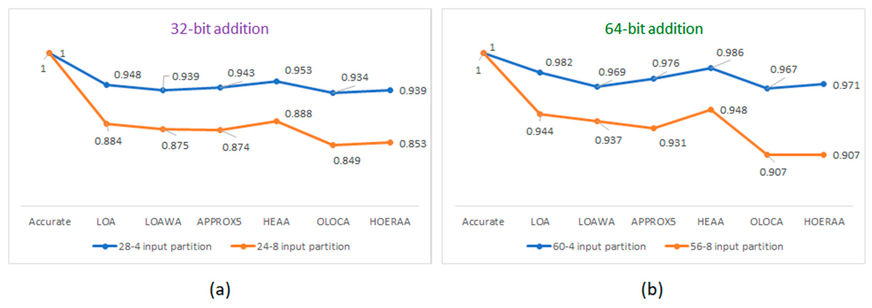
The power-delay products (PDPs) of accurate and approximate adders were calculated by multiplying the minimum clock period with the total on-chip power. The PDPs of the adders were subsequently normalized. To perform the normalization, the maximum PDP (corresponding to the accurate FPGA adder) was considered as the reference and this PDP was used to divide the PDPs of all the approximate adders corresponding to a particular addition operation. It is desirable for power and delay to be at a minimum for a digital circuit and, hence, the PDP is also desirable to be at a minimum. Hence, the least value of PDP corresponding to an adder is reflective of a low power/energy-efficient design. The normalized PDPs of FPGA-based accurate and approximate adders, with respect to 32- and 64-bit additions, are plotted in Figure 2a,b respectively.
Figure 2a,b show the reduction in energy achieved by increasing the approximation from 4-bits to 8-bits in the approximate adders for 32- and 64-bit additions. In the case of 32-bit addition, OLOCA achieves the least PDP for both the input partitions. In the case of 64-bit addition, OLOCA achieves the least PDP for a 60-4 input partition while OLOCA and HOERAA achieve the least PDP for a 56-8 input partition. Compared to the accurate 32-bit FPGA adder, HOERAA reports a 6.1% reduction in energy for a 28-4 input partition and a 14.7% reduction in energy for a 24-8 input partition. On the other hand, in comparison with the accurate 64-bit FPGA adder, HOERAA reports a 3% reduction in energy with a 60-4 input partition and a 9.3% reduction in energy with a 56-8 input partition. Further, HOERAA achieves better energy efficiency compared to the accurate FPGA adder while consuming less FPGA resources (LUTs and FFs).
The percentage of energy reduction achieved is relatively less for 64-bit addition compared to 32-bit addition. This is because the size of the accurate sub-adder is greater in the case of the former compared to the latter. Hence, another general inference is that a relatively small approximate adder will exhibit an enhanced design optimization compared to a larger approximate adder for the same approximation. This is because the ratio of bits allotted to the accurate sub-adder vis-à-vis the inaccurate sub-adder would be greater in a larger adder (for example, 15:1 in a 64-bit approximate adder with K = 4) compared to a smaller adder (for example, 7:1 in a 32-bit approximate adder with K = 4). The design metrics corresponding to the accurate sub-adder would dominate the design metrics of the approximate adder when increasing the size of the accurate sub-adder while keeping the size of the inaccurate sub-adder as a constant. Thus, as the size of the accurate sub-adder in an approximate adder increases, the savings in design metrics obtained through approximation are reduced.
4.2. ASIC-Based Implementation Results
For an ASIC-based implementation, a 32/28nm CMOS-based standard digital cell library [29] was considered for the implementations. An efficient accurate carry-lookahead adder (CLA) recently presented in Reference [30] was considered. The new CLA of Reference [30] is called the factorized recursive CLA, i.e., FRCLA, which is used to realize the accurate adder of Figure 1a. The approximate adders shown in Figure 1b–g were implemented with the FRCLA used to realize the accurate sub-adders. The accurate and approximate adders were implemented using a high-Vt 32/28 nm CMOS technology. The simulation environment corresponds to a typical-case specification of the standard digital cell library with a recommended supply voltage of 1.05 V and an operating junction temperature of 25 °C. The simulation set-up was maintained the same as in Reference [29]. The critical path delay, silicon area, and average power dissipation of the adders were estimated using Synopsys tools. To estimate the average power dissipation, about 1000 random input vectors were identically supplied to the adders at time intervals of 5 ns (200 MHz), as done in Reference [29]. The switching activities captured through the functional simulations were subsequently used to estimate the average power dissipation. The critical path delays and area occupancies were estimated with default wire loads included while performing the simulations. The time-based power analysis mode of Synopsys PrimeTime was invoked to estimate the average power dissipation. The estimated ASIC-based design metrics are given in Table 2.
Referring to Table 2, it is seen that the critical path delays of the approximate adders corresponding to a particular addition are almost the same for a similar approximation. For example, all the 32-bit approximate adders with a 24-8 input partition have the same critical path delay of 0.96ns. This is because the critical path delays of the approximate adders are underpinned by the critical path delays of the accurate sub-adders, which are realized using the FRCLA architecture. In terms of area, LOAWA and APPROX5 consume less silicon compared to the accurate and other approximate adders for 32- and 64-bit additions. OLOCA dissipates less power compared to the accurate and other approximate adders for 32- and 64-bit additions.
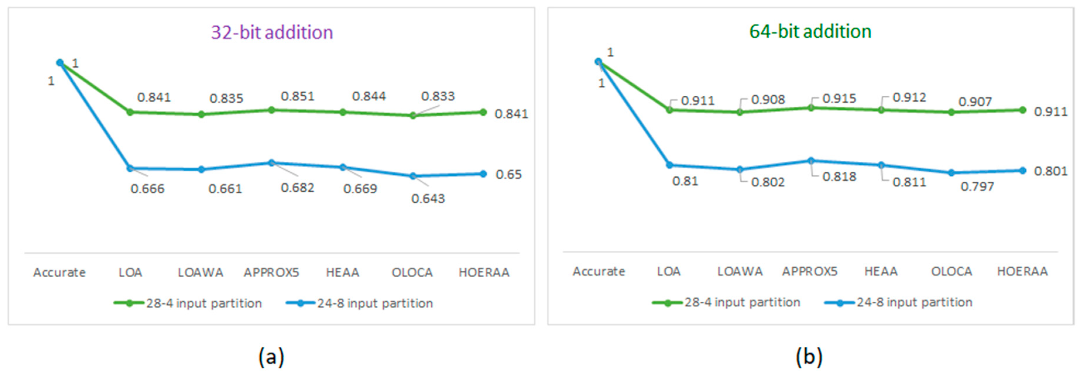
A perusal of Table 2 confirms the general observation made on the basis of Table 1 that increasing the approximation size (from 4-bits to 8-bits) in an approximate adder helps to better optimize the design metrics by reducing the critical path delay, silicon area, and average power simultaneously. This is found to be true for 32-bit and 64-bit approximate adders employing two approximations with K = 4 and K = 8. For example, a 32-bit HOERAA with a 28-4 input partition reports a 7.8% reduction in delay, a 10% reduction in area, and an 8.8% reduction in power compared to the accurate 32-bit FRCLA, and a 32-bit HOERAA with a 24-8 input partition reports enhanced reductions in delay, area, and power by 15.7%, 21.4%, and 23%, respectively, compared to the accurate 32-bit FRCLA. On the other hand, a 64-bit HOERAA with a 60-4 input partition reports a 4.8% reduction in delay, a 5% reduction in area, and a 4.4% reduction in power compared to the accurate 32-bit FRCLA, while a 64-bit HOERAA with a 56-8 input partition reports enhanced reductions in delay, area, and power by 9.6%, 10.7%, and 11.4%, respectively, compared to the accurate 64-bit FRCLA. As noted earlier, the relatively less percentage reductions in design metrics achieved for 64-bit approximate adders compared to 32-bit approximate adders are attributed to the increase in the size of the accurate sub-adders for the former compared to the latter. The PDPs of accurate and approximate adders were calculated from the delay and power values given in Table 2. The normalized PDP plots corresponding to the ASIC-based designs of accurate and approximate adders for 32- and 64-bit additions are shown in Figure 3a,b. The normalization was performed in the same manner as discussed earlier in the context of Figure 2. Figure 3a,b show that OLOCA has the least PDP, which is closely followed by HOERAA.
4.3. Error Characteristics of Approximate Adders
It is important to ascertain the error characteristics of the approximate adders to determine which of them would have a less error while providing a maximum implementation performance (i.e., better optimized design metrics). This an important focus of this work, where the error characteristic is given an equal weightage as the quality-of-results (design metrics).
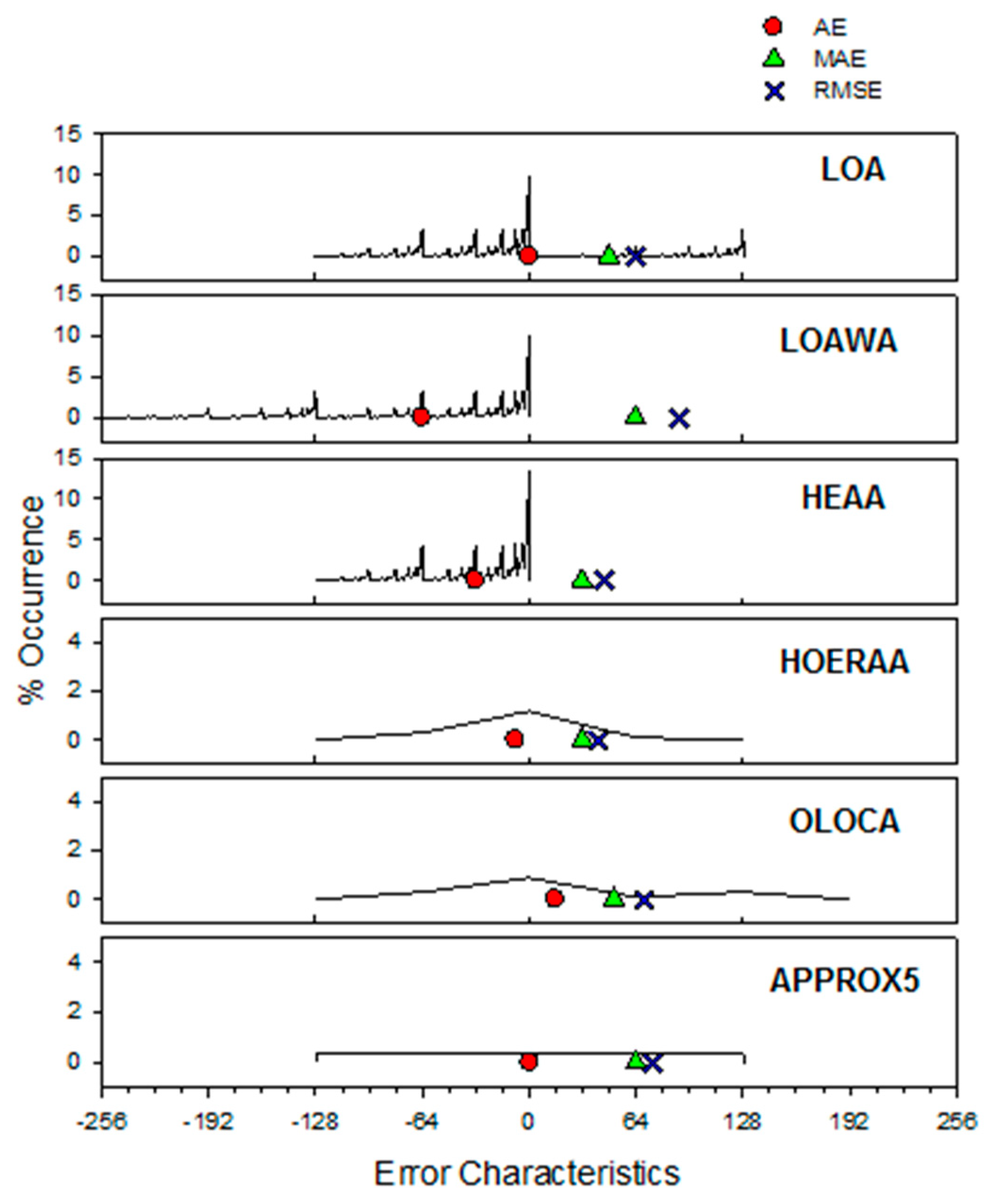
Many error metrics have been proposed in the literature for approximate computing. In this paper, we used the standard error metrics such as the average error (AE), the mean average error (MAE, also referred to as mean error distance (MED) in the literature), and the root mean square error (RMSE) [31] for the approximate adders, as they are more widely used in error analysis. The error metrics and the error bounds of the approximate adders are given in Table 3. The error metrics, such as AE, MAE, and RMSE, have again been calculated by using a 4-bit and an 8-bit inaccurate sub-adder for the approximate adders shown in Figure 1b–g, experimentally, by considering all the distinct inputs corresponding to the inaccurate sub-adders. The generalized error range for the approximate adders having a K-bit inaccurate sub-adder is also given in Table 3 (last column). No error is applicable for the accurate adder shown in Figure 1a.
We consider RMSE as a more important error metric in this work since it has been observed in Reference [27] that RMSE gives a relatively higher weight to larger errors and is considered more likely to impact an application employing approximate arithmetic. AE, MAE, and RMSE are expressed as follows:
In Equations (1), (2), and (3), ‘N’ represents the adder size, ‘e’ is the error distance (i.e., the numerical difference between the accurate and approximate adder output), ‘P’ denotes the probability of an error value occurrence, and ‘δ’ is the set of all error values.
From Table 3, it is seen that HOERAA has a reduced RMSE compared to the other approximate adders for K = 4 and K = 8. While comparing with OLOCA, which has the same speed as HOERAA, evident from Table 1 and Table 2, HOERAA reports a 50% reduction in AE, a 39.5% reduction in MAE, and a 40.7% reduction in RMSE for K = 4, and a 50% reduction in AE, a 38.5% reduction in MAE, and a 40.2% reduction in RMSE for K = 8.
It would also be useful to study the distribution of errors of the approximate adders about the zero error. The results of this error distribution analysis, which assumes a uniform distribution of inputs, are captured in Figure 4. The percentage occurrence of errors corresponding to the specified error bounds (range), given in Table 3, are plotted in the Y-axis and the error bounds are plotted in the X-axis in Figure 4. It can be seen from Figure 4 that HOERAA has a better near normal distribution about the zero error. APPROX5 also has a good error distribution about the zero error. However, APPROX5 reports substantial increases in MAE and RMSE by 103.2% and 80.4% on average, compared to HOERAA, when considering 4-bit and 8-bit inaccurate sub-adders in the approximate adders, which is undesirable.
5. Conclusions
This article has presented a new approximate adder called HOERAA, which is suitable for FPGA- and ASIC-based implementations. In this work, we considered a subset of approximate adders for comparison, which are also suitable for FPGA- and ASIC-based implementations. It has been observed that HOERAA achieves a good optimization in the design metrics compared to the other approximate adders whilst reporting reduced error characteristics.
Considering a FPGA-based implementation with a 8-bit inaccurate sub-adder, HOERAA requires 22% fewer LUTs and 18.6% fewer registers for 32-bit addition while improving the maximum frequency by 7.7% and reducing the PDP by 14.7% compared to the native accurate FPGA adder, and for 64-bit addition, HOERAA requires 11% fewer LUTs and 9.3% fewer registers while increasing the maximum frequency by 9.1% and reducing the PDP by 9.3%.
Considering an ASIC-based implementation using a standard digital cell library, and compared to the accurate FRCLA, HOERAA with an 8-bit inaccurate sub-adder achieves a 15.7% reduction in critical path delay, a 21.4% reduction in area, and a 35% reduction in PDP for 32-bit addition, and a 15.3% reduction in critical path delay, a 10.7% reduction in area, and a 20% reduction in PDP for 64-bit addition.
We also considered FPGA- and ASIC-based implementations of 32-bit and 64-bit approximate adders using a 4-bit inaccurate sub-adder. This was done mainly to analyze the trends in the design metrics when the approximation size is increased from 4-bits to 8-bits in the least significant adder bit positions. It was inferred that, for both FPGA- and ASIC-based implementations, increasing the size of the inaccurate sub-adder has a beneficial impact on the optimization of design metrics. However, this would be accompanied by some decrease in the accuracy. This points to a potential trade-off between accuracy and optimization of the design metrics that is inherent in approximate computing.
AE, MAE, and RMSE are standard error metrics, which are usually quantified when performing approximate computer arithmetic [31]. It is mentioned in Reference [27] that RMSE gives a relatively greater weight to larger errors and it is mentioned in Reference [32] that MAE (also called MED) is an effective metric for measuring the implementation accuracy of an approximate adder. Overall, HOERAA has reduced error attributes compared to the other approximate adders. Notably, in comparison with OLOCA, which has nearly similar design metrics as HOERAA, the latter achieves significant reductions in the error metrics viz. a 39% reduction in MAE and a 40.5% reduction in RMSE, on average, when considering the use of 4-bit and 8-bit inaccurate sub-adders.
Overall, from the perspectives of hardware design optimization and error reduction, HOERAA is preferable to the rest, including the recently proposed OLOCA. In the future, we would consider utilizing HOERAA for constructing an approximate multiplier. These could then be considered for realizing low power/energy-efficient computation units for use in practical digital signal processing applications such as image/audio/video processing.
Author Contributions
Conceptualization, P.B. and D.L.M.; methodology, P.B. and D.L.M.; investigation, P.B. and D.L.M.; validation, P.B.; resources, D.L.M.; data curation, P.B.; writing—original draft preparation, P.B.; writing – review and editing, P.B. and D.L.M.; project administration, D.L.M. and P.B.; funding acquisition, D.L.M.
Funding
This research is supported by the Academic Research Fund Tier-2 research award of the Ministry of Education (MOE), Singapore under Grant MOE2018-T2-2-024.
Conflicts of Interest
The authors declare no conflict of interest. The funders had no role in the design of the study; in the collection, analyses, or interpretation of data; in the writing of the manuscript, or in the decision to publish the results.
References
- Han, J.; Orshansky, M. Approximate computing: An emerging paradigm for energy-efficient design. In Proceedings of the 18th IEEE European Test Symposium, Avignon, France, 27–31 May 2013. [Google Scholar]
- Nair, R. Big data needs approximate computing: Technical perspective. Commun. ACM 2015, 58, 104. [Google Scholar] [CrossRef]
- Sampson, A.; Deitl, W.; Fortuna, D.; Gnanapragasam, D.; Ceze, L.; Grossman, D. EnerJ: Approximate data types for safe and general low-power computation. ACM SIGPLAN Not. 2011, 46, 164–174. [Google Scholar] [CrossRef]
- Panda, P.; Sengupta, A.; Sarwar, S.S.; Srinivasan, G.; Venkataramani, S.; Raghunathan, A.; Roy, K. Cross-layer approximations for neuromorphic computing: From devices to circuits and systems. In Proceedings of the 53rd Design Automation Conference, Austin, TX, USA, 5–9 June 2016. [Google Scholar]
- Sarwar, S.S.; Srinivasan, G.; Han, B.; Wijesinghe, P.; Jaiswal, A.; Panda, P.; Raghunathan, A.; Roy, K. Energy efficient neural computing: A study of cross-layer approximations. IEEE J. Emerg. Sel. Top. Circuits Syst. 2018, 8, 796–809. [Google Scholar] [CrossRef]
- Venkataramani, S.; Chakradhar, S.T.; Roy, K.; Raghunathan, A. Approximate computing and the quest for computing efficiency. In Proceedings of the 52nd Design Automation Conference, San Francisco, CA, USA, 7–11 June 2015. [Google Scholar]
- Shoushtari, M.; Rahmani, A.M.; Dutt, N. Quality-configurable memory hierarchy through approximation. In Proceedings of the International Conference on Compilers, Architecture, and Synthesis for Embedded Systems, Seoul, Korea, 15–20 October 2017. [Google Scholar]
- Sampson, K.; Nelson, J.; Strauss, K.; Ceze, L. Approximate storage in solid-state memories. ACM Trans. Comput. Syst. 2014, 32, 9:1–9:23. [Google Scholar] [CrossRef]
- Zhang, H.; Putic, M.; Lach, J. Low power GPGPU computation with imprecise hardware. In Proceedings of the 51st Design Automation Conference, San Francisco, CA, USA, 1–5 June 2014. [Google Scholar]
- Schlachter, J.; Camus, V.; Enz, C. Near/sub-threshold circuits and approximate computing: The perfect combination for ultra-low-power systems. In Proceedings of the IEEE Computer Society Annual Symposium on VLSI, Montpellier, France, 8–10 July 2015. [Google Scholar]
- Breuer, M.A.; Zhu, H. Error-tolerance and multi-media. In Proceedings of the International Conference on Intelligent Information Hiding and Multimedia Signal Processing, Pasadena, CA, USA, 18–20 December 2006. [Google Scholar]
- Venkataramani, S.; Sabne, A.; Kozhikkottu, V.; Roy, K.; Raghunathan, A. SALSA: Systematic logic synthesis of approximate circuits. In Proceedings of the 49th Design Automation Conference, San Francisco, CA, USA, 3–7 June 2012. [Google Scholar]
- Jiang, H.; Liu, C.; Liu, L.; Lombardi, F.; Han, J. A review, classification, and comparative evaluation of approximate arithmetic circuits. ACM J. Emerg. Technol. Comput. Syst. 2017, 13, 60:1–60:34. [Google Scholar] [CrossRef]
- Zhu, N.; Goh, W.L.; Zhang, W.; Yeo, K.S.; Kong, Z.H. Design of low-power high-speed truncation-error-tolerant adder and its application in digital signal processing. IEEE Trans. VLSI Syst. 2010, 18, 1225–1229. [Google Scholar]
- Zhu, N.; Goh, W.L.; Yeo, K.S. An enhanced low-power high-speed adder for error-tolerant application. In Proceedings of the 12th International Symposium on Integrated Circuits, Singapore, 14–16 December 2009. [Google Scholar]
- Zhu, N.; Goh, W.L.; Wang, G.; Yeo, K.S. Enhanced low-power high-speed adder for error-tolerant application. In Proceedings of the International SoC Design Conference, Incheon, Korea, 22–23 November 2010. [Google Scholar]
- Yang, Z.; Jain, A.; Liang, J.; Han, J.; Lombardi, F. Approximate XOR/XNOR-based adders for inexact computing. In Proceedings of the 13th IEEE International Conference on Nanotechnology, Beijing, China, 5–8 August 2013. [Google Scholar]
- Gupta, V.; Mohapatra, D.; Raghunathan, A.; Roy, K. Low-power digital signal processing using approximate adders. IEEE Trans. CAD Integr. Circuits Syst. 2013, 32, 124–137. [Google Scholar] [CrossRef]
- Mahdiani, H.R.; Ahmadi, A.; Fakhraie, S.M.; Lucas, C. Bio-inspired computational blocks for efficient VLSI implementation of soft-computing applications. IEEE Trans. Circuits Syst. I Regul. Pap. 2010, 57, 850–862. [Google Scholar] [CrossRef]
- Albicocco, P.; Cardarilli, G.C.; Nannarelli, A.; Petricca, M.; Re, M. Imprecise arithmetic for low power image processing. In Proceedings of the 46th Asilomar Conference on Signals, Systems and Computers, Pacific Grove, CA, USA, 4–7 November 2012. [Google Scholar]
- Dalloo, A.; Najafi, A.; Garcia-Ortiz, A. Systematic design of an approximate adder: The optimized lower part constant-OR adder. IEEE Trans. VLSI Syst. 2018, 26, 1595–1599. [Google Scholar] [CrossRef]
- Echavarria, J.; Wildermann, S.; Becher, A.; Teich, J.; Ziener, D. FAU: Fast and error-optimized approximate adder units on LUT-based FPGAs. In Proceedings of the International Conference on Field-Programmable Technology, Xi’an, China, 7–9 December 2016. [Google Scholar]
- Verma, A.K.; Brisk, P.; Ienne, P. Variable latency speculative addition: A new paradigm for arithmetic circuit design. In Proceedings of the Design, Automation and Test in Europe, Munich, Germany, 10–14 March 2008. [Google Scholar]
- Kahng, A.B.; Kang, S. Accuracy-configurable adder for approximate arithmetic designs. In Proceedings of the 49th Design Automation Conference, San Francisco, CA, USA, 3–7 June 2012. [Google Scholar]
- Ye, R.; Wang, T.; Yuan, F.; Kumar, R.; Xu, Q. On reconfiguration-oriented approximate adder design and its application. In Proceedings of the IEEE/ACM International Conference on Computer-Aided Design, San Jose, CA, USA, 28–31 October 2013. [Google Scholar]
- Shafique, M.; Ahmad, W.; Hafiz, R.; Henkel, J. A low latency generic accuracy configurable adder. In Proceedings of the 52nd Design Automation Conference, San Francisco, CA, USA, 7–11 June 2015. [Google Scholar]
- Balasubramanian, P.; Maskell, D. Hardware efficient approximate adder design. In Proceedings of the IEEE Region 10 Conference, Jeju, Korea, 28–31 October 2018. [Google Scholar]
- Raha, A.; Jayakumar, H.; Raghunathan, V. Input-based dynamic reconfiguration of approximate arithmetic units for video encoding. IEEE Trans. VLSI Syst. 2016, 24, 846–857. [Google Scholar] [CrossRef]
- Synopsys SAED_EDK32/28_CORE Databook. Revision 1.0.0. January 2012. Available online: https://www.synopsys.com/community/university-program/teaching-resources.html (accessed on 29 May 2019).
- Balasubramanian, P.; Maskell, D.L. Factorized carry lookahead adders. In Proceedings of the IEEE 14th International Symposium on Signals, Circuits and Systems, Iasi, Romania, 11–12 July 2019. [Google Scholar]
- Wu, Y.; Li, Y.; Ge, X.; Gao, Y.; Qian, W. An efficient method for calculating the error statistics of block-based approximate adders. IEEE Trans. Comput. 2019, 68, 21–38. [Google Scholar] [CrossRef]
- Liang, J.; Han, J.; Lombardi, F. New metrics for the reliability of approximate and probabilistic adders. IEEE Trans. Comput. 2013, 62, 1760–1771. [Google Scholar] [CrossRef]
Figure 1.
Block schematics of N-bit accurate and approximate adders.

Figure 2.
Normalized PDP plots of accurate and approximate FPGA-based adders corresponding to: (a) 32-bit addition and (b) 64-bit addition.
Figure 2.
Normalized PDP plots of accurate and approximate FPGA-based adders corresponding to: (a) 32-bit addition and (b) 64-bit addition.

Figure 3.
Normalized power-delay product (PDP) plots of accurate and approximate ASIC-based adders corresponding to: (a) 32-bit addition and (b) 64-bit addition.
Figure 3.
Normalized power-delay product (PDP) plots of accurate and approximate ASIC-based adders corresponding to: (a) 32-bit addition and (b) 64-bit addition.

Figure 4.
Error distribution of approximate adders about the normal (zero) error.


Table 1.
Field programmable gate array (FPGA)-based implementation results (post-place and route) for 32- and 64-bit accurate and approximate adders using Xilinx Vivado 2018.3, targeting an Artix-7 FPGA. LUT, look-up tables; FF, flip-flops; LOA, lower-part OR adder; LOAWA, LOA without the 2-input AND function; HEAA, hardware-efficient approximate adder; OLOCA, optimized version of LOA; HOERAA, hardware optimized and error reduced approximate adder.
| Type of Adder | FPGA-Based Design Metrics | ||||
|---|---|---|---|---|---|
| Clock Period (ns) | Maximum Frequency (MHz) | Total Power (W) | # LUTs | # FFs | |
| 32-bit addition | |||||
| Accurate (FPGA adder) | 2.10 | 476.19 | 0.209 | 32 | 97 |
| Using a 28-4 input partition for the approximate adders (i.e., K = 4) | |||||
| LOA | 2.03 | 492.61 | 0.205 | 30 | 97 |
| LOAWA | 2.01 | 497.51 | 0.205 | 30 | 97 |
| APPROX5 | 2.00 | 500.00 | 0.207 | 28 | 94 |
| HEAA | 2.03 | 492.61 | 0.206 | 30 | 97 |
| OLOCA | 2.04 | 490.20 | 0.201 | 29 | 91 |
| HOERAA | 2.04 | 490.20 | 0.202 | 29 | 91 |
| Using a 24-8 input partition for the approximate adders (i.e., K = 8) | |||||
| LOA | 1.94 | 515.46 | 0.200 | 28 | 97 |
| LOAWA | 1.92 | 520.83 | 0.200 | 28 | 97 |
| APPROX5 | 1.90 | 526.32 | 0.202 | 24 | 90 |
| HEAA | 1.94 | 515.46 | 0.201 | 28 | 97 |
| OLOCA | 1.95 | 512.82 | 0.191 | 25 | 79 |
| HOERAA | 1.95 | 512.82 | 0.192 | 25 | 79 |
| 64-bit addition | |||||
| Accurate (FPGA adder) | 2.89 | 346.02 | 0.264 | 64 | 193 |
| Using a 60-4 input partition for the approximate adders (i.e., K = 4) | |||||
| LOA | 2.85 | 350.88 | 0.263 | 62 | 193 |
| LOAWA | 2.80 | 357.14 | 0.264 | 62 | 193 |
| APPROX5 | 2.83 | 353.36 | 0.263 | 60 | 190 |
| HEAA | 2.85 | 350.88 | 0.264 | 62 | 193 |
| OLOCA | 2.86 | 349.65 | 0.258 | 61 | 187 |
| HOERAA | 2.86 | 349.65 | 0.259 | 61 | 187 |
| Using a 56-8 input partition for the approximate adders (i.e., K = 8) | |||||
| LOA | 2.77 | 361.01 | 0.260 | 60 | 193 |
| LOAWA | 2.77 | 361.01 | 0.258 | 60 | 193 |
| APPROX5 | 2.68 | 373.13 | 0.265 | 56 | 186 |
| HEAA | 2.77 | 361.01 | 0.261 | 60 | 193 |
| OLOCA | 2.65 | 377.36 | 0.261 | 57 | 175 |
| HOERAA | 2.65 | 377.36 | 0.261 | 57 | 175 |
Table 2.
ASIC-based design metrics corresponding to accurate and approximate 32-bit and 64-bit adders estimated using a 32/28nm CMOS process.
Table 2.
ASIC-based design metrics corresponding to accurate and approximate 32-bit and 64-bit adders estimated using a 32/28nm CMOS process.
| Type of Adder | Delay (ns) | Area (µm2) | Power (µW) |
|---|---|---|---|
| 32-bit addition | |||
| Accurate (FRCLA) | 1.15 | 532.69 | 37.04 |
| Using a 28-4 input partition for the approximate adders (i.e., K = 4) | |||
| LOA | 1.06 | 476.27 | 33.81 |
| LOAWA | 1.06 | 474.23 | 33.57 |
| APPROX5 | 1.06 | 474.23 | 34.18 |
| HEAA | 1.06 | 479.57 | 33.93 |
| OLOCA | 1.06 | 474.74 | 33.49 |
| HOERAA | 1.06 | 480.08 | 33.79 |
| Using a 24-8 input partition for the approximate adders (i.e., K = 8) | |||
| LOA | 0.97 | 417.81 | 29.26 |
| LOAWA | 0.97 | 415.78 | 29.02 |
| APPROX5 | 0.97 | 415.78 | 29.94 |
| HEAA | 0.97 | 421.12 | 29.38 |
| OLOCA | 0.97 | 413.24 | 28.24 |
| HOERAA | 0.97 | 418.58 | 28.54 |
| 64-bit addition | |||
| Accurate (FRCLA) | 1.88 | 1065.37 | 74.37 |
| Using a 60-4 input partition for the approximate adders (i.e., K = 4) | |||
| LOA | 1.79 | 1008.95 | 71.14 |
| LOAWA | 1.79 | 1006.92 | 70.90 |
| APPROX5 | 1.79 | 1006.92 | 71.50 |
| HEAA | 1.79 | 1012.26 | 71.26 |
| OLOCA | 1.79 | 1007.43 | 70.82 |
| HOERAA | 1.79 | 1012.76 | 71.12 |
| Using a 56-8 input partition for the approximate adders (i.e., K = 8) | |||
| LOA | 1.70 | 950.50 | 66.58 |
| LOAWA | 1.69 | 948.47 | 66.34 |
| APPROX5 | 1.70 | 948.47 | 67.26 |
| HEAA | 1.70 | 953.80 | 66.70 |
| OLOCA | 1.70 | 945.92 | 65.56 |
| HOERAA | 1.70 | 951.26 | 65.86 |
Table 3.
Error metrics of the approximate adders shown in Figure 1b–g. Average error (AE), mean average error (MAE), and root mean square error (RMSE) were calculated by considering a 4-bit and an 8-bit inaccurate sub-adder (i.e., K = 4 and K = 8) in the approximate adders. The generalized error range of the approximate adders using a K-bit inaccurate sub-adder is also specified.
| Type of Adder | Error Characteristics | ||||||
|---|---|---|---|---|---|---|---|
| AE | MAE | RMSE | Error Range | ||||
| K = 4 | K = 8 | K = 4 | K = 8 | K = 4 | K = 8 | ||
| Accurate | Nil | Nil | Nil | Nil | |||
| LOA | 0.25 | 0.25 | 2.875 | 47.875 | 4 | 64 | −(2K–1–1) to 2K–1 |
| LOAWA | −3.75 | −63.75 | 3.75 | 63.75 | 5.477 | 90.33 | −(2K–1) to 0 |
| APPROX5 | 0.5 | 0.5 | 4 | 64 | 4.637 | 73.9 | −(2K–1–1) to 2K–1 |
| HEAA | −1.75 | −31.75 | 1.75 | 31.75 | 2.646 | 45.08 | −(2K–1–1) to 0 |
| OLOCA | 1 | 16 | 3.203 | 51.997 | 4.301 | 69.13 | −(2K–1–1) to (2K–1+2K–2–1) |
| HOERAA | −0.5 | −8 | 1.938 | 31.996 | 2.550 | 41.31 | −(2K–1–1) to (2K–1–1) |
© 2019 by the authors. Licensee MDPI, Basel, Switzerland. This article is an open access article distributed under the terms and conditions of the Creative Commons Attribution (CC BY) license (http://creativecommons.org/licenses/by/4.0/).
Share and Cite
MDPI and ACS Style
Balasubramanian, P.; Maskell, D.L. Hardware Optimized and Error Reduced Approximate Adder. Electronics 2019, 8, 1212. https://0-doi-org.brum.beds.ac.uk/10.3390/electronics8111212
AMA Style
Balasubramanian P, Maskell DL. Hardware Optimized and Error Reduced Approximate Adder. Electronics. 2019; 8(11):1212. https://0-doi-org.brum.beds.ac.uk/10.3390/electronics8111212
Chicago/Turabian StyleBalasubramanian, Padmanabhan, and Douglas L. Maskell. 2019. "Hardware Optimized and Error Reduced Approximate Adder" Electronics 8, no. 11: 1212. https://0-doi-org.brum.beds.ac.uk/10.3390/electronics8111212
Note that from the first issue of 2016, this journal uses article numbers instead of page numbers. See further details here.